WO2016017444A1 - 光センサ - Google Patents
光センサ Download PDFInfo
- Publication number
- WO2016017444A1 WO2016017444A1 PCT/JP2015/070474 JP2015070474W WO2016017444A1 WO 2016017444 A1 WO2016017444 A1 WO 2016017444A1 JP 2015070474 W JP2015070474 W JP 2015070474W WO 2016017444 A1 WO2016017444 A1 WO 2016017444A1
- Authority
- WO
- WIPO (PCT)
- Prior art keywords
- light
- light receiving
- receiving element
- optical waveguide
- fixing member
- Prior art date
- Legal status (The legal status is an assumption and is not a legal conclusion. Google has not performed a legal analysis and makes no representation as to the accuracy of the status listed.)
- Ceased
Links
Images



Classifications
-
- H—ELECTRICITY
- H10—SEMICONDUCTOR DEVICES; ELECTRIC SOLID-STATE DEVICES NOT OTHERWISE PROVIDED FOR
- H10F—INORGANIC SEMICONDUCTOR DEVICES SENSITIVE TO INFRARED RADIATION, LIGHT, ELECTROMAGNETIC RADIATION OF SHORTER WAVELENGTH OR CORPUSCULAR RADIATION
- H10F30/00—Individual radiation-sensitive semiconductor devices in which radiation controls the flow of current through the devices, e.g. photodetectors
-
- G—PHYSICS
- G01—MEASURING; TESTING
- G01J—MEASUREMENT OF INTENSITY, VELOCITY, SPECTRAL CONTENT, POLARISATION, PHASE OR PULSE CHARACTERISTICS OF INFRARED, VISIBLE OR ULTRAVIOLET LIGHT; COLORIMETRY; RADIATION PYROMETRY
- G01J1/00—Photometry, e.g. photographic exposure meter
- G01J1/02—Details
- G01J1/04—Optical or mechanical part supplementary adjustable parts
- G01J1/0407—Optical elements not provided otherwise, e.g. manifolds, windows, holograms, gratings
- G01J1/0425—Optical elements not provided otherwise, e.g. manifolds, windows, holograms, gratings using optical fibers
-
- G—PHYSICS
- G01—MEASURING; TESTING
- G01J—MEASUREMENT OF INTENSITY, VELOCITY, SPECTRAL CONTENT, POLARISATION, PHASE OR PULSE CHARACTERISTICS OF INFRARED, VISIBLE OR ULTRAVIOLET LIGHT; COLORIMETRY; RADIATION PYROMETRY
- G01J1/00—Photometry, e.g. photographic exposure meter
- G01J1/02—Details
- G01J1/0204—Compact construction
-
- G—PHYSICS
- G01—MEASURING; TESTING
- G01J—MEASUREMENT OF INTENSITY, VELOCITY, SPECTRAL CONTENT, POLARISATION, PHASE OR PULSE CHARACTERISTICS OF INFRARED, VISIBLE OR ULTRAVIOLET LIGHT; COLORIMETRY; RADIATION PYROMETRY
- G01J1/00—Photometry, e.g. photographic exposure meter
- G01J1/02—Details
- G01J1/0204—Compact construction
- G01J1/0209—Monolithic
-
- G—PHYSICS
- G01—MEASURING; TESTING
- G01J—MEASUREMENT OF INTENSITY, VELOCITY, SPECTRAL CONTENT, POLARISATION, PHASE OR PULSE CHARACTERISTICS OF INFRARED, VISIBLE OR ULTRAVIOLET LIGHT; COLORIMETRY; RADIATION PYROMETRY
- G01J1/00—Photometry, e.g. photographic exposure meter
- G01J1/02—Details
- G01J1/04—Optical or mechanical part supplementary adjustable parts
- G01J1/0403—Mechanical elements; Supports for optical elements; Scanning arrangements
-
- G—PHYSICS
- G01—MEASURING; TESTING
- G01J—MEASUREMENT OF INTENSITY, VELOCITY, SPECTRAL CONTENT, POLARISATION, PHASE OR PULSE CHARACTERISTICS OF INFRARED, VISIBLE OR ULTRAVIOLET LIGHT; COLORIMETRY; RADIATION PYROMETRY
- G01J1/00—Photometry, e.g. photographic exposure meter
- G01J1/02—Details
- G01J1/04—Optical or mechanical part supplementary adjustable parts
- G01J1/0407—Optical elements not provided otherwise, e.g. manifolds, windows, holograms, gratings
-
- G—PHYSICS
- G01—MEASURING; TESTING
- G01J—MEASUREMENT OF INTENSITY, VELOCITY, SPECTRAL CONTENT, POLARISATION, PHASE OR PULSE CHARACTERISTICS OF INFRARED, VISIBLE OR ULTRAVIOLET LIGHT; COLORIMETRY; RADIATION PYROMETRY
- G01J1/00—Photometry, e.g. photographic exposure meter
- G01J1/02—Details
- G01J1/04—Optical or mechanical part supplementary adjustable parts
- G01J1/0407—Optical elements not provided otherwise, e.g. manifolds, windows, holograms, gratings
- G01J1/0414—Optical elements not provided otherwise, e.g. manifolds, windows, holograms, gratings using plane or convex mirrors, parallel phase plates, or plane beam-splitters
-
- G—PHYSICS
- G01—MEASURING; TESTING
- G01J—MEASUREMENT OF INTENSITY, VELOCITY, SPECTRAL CONTENT, POLARISATION, PHASE OR PULSE CHARACTERISTICS OF INFRARED, VISIBLE OR ULTRAVIOLET LIGHT; COLORIMETRY; RADIATION PYROMETRY
- G01J1/00—Photometry, e.g. photographic exposure meter
- G01J1/42—Photometry, e.g. photographic exposure meter using electric radiation detectors
- G01J1/4204—Photometry, e.g. photographic exposure meter using electric radiation detectors with determination of ambient light
-
- G—PHYSICS
- G02—OPTICS
- G02B—OPTICAL ELEMENTS, SYSTEMS OR APPARATUS
- G02B6/00—Light guides; Structural details of arrangements comprising light guides and other optical elements, e.g. couplings
- G02B6/24—Coupling light guides
- G02B6/42—Coupling light guides with opto-electronic elements
-
- H—ELECTRICITY
- H10—SEMICONDUCTOR DEVICES; ELECTRIC SOLID-STATE DEVICES NOT OTHERWISE PROVIDED FOR
- H10F—INORGANIC SEMICONDUCTOR DEVICES SENSITIVE TO INFRARED RADIATION, LIGHT, ELECTROMAGNETIC RADIATION OF SHORTER WAVELENGTH OR CORPUSCULAR RADIATION
- H10F77/00—Constructional details of devices covered by this subclass
- H10F77/40—Optical elements or arrangements
-
- G—PHYSICS
- G02—OPTICS
- G02B—OPTICAL ELEMENTS, SYSTEMS OR APPARATUS
- G02B6/00—Light guides; Structural details of arrangements comprising light guides and other optical elements, e.g. couplings
- G02B6/10—Light guides; Structural details of arrangements comprising light guides and other optical elements, e.g. couplings of the optical waveguide type
- G02B6/12—Light guides; Structural details of arrangements comprising light guides and other optical elements, e.g. couplings of the optical waveguide type of the integrated circuit kind
- G02B2006/12133—Functions
- G02B2006/12138—Sensor
-
- G—PHYSICS
- G02—OPTICS
- G02B—OPTICAL ELEMENTS, SYSTEMS OR APPARATUS
- G02B6/00—Light guides; Structural details of arrangements comprising light guides and other optical elements, e.g. couplings
- G02B6/24—Coupling light guides
- G02B6/42—Coupling light guides with opto-electronic elements
- G02B6/4201—Packages, e.g. shape, construction, internal or external details
- G02B6/4204—Packages, e.g. shape, construction, internal or external details the coupling comprising intermediate optical elements, e.g. lenses, holograms
- G02B6/4214—Packages, e.g. shape, construction, internal or external details the coupling comprising intermediate optical elements, e.g. lenses, holograms the intermediate optical element having redirecting reflective means, e.g. mirrors, prisms for deflecting the radiation from horizontal to down- or upward direction toward a device
Definitions
- Thin devices such as the above TVs are required to be thin.
- the light receiving element 4 is directly used to receive light in the optical sensor, there is a limit to the reduction in the thickness of the portion where the light receiving element 4 is installed due to the size of the light receiving element 4 itself. The demand for thinning cannot be fully met.
- the light receiving element 4 is mounted on an electric board (not shown), and the electric board also prevents thinning. Furthermore, since the light receiving element 4 is normally used as the optical sensor in a state of being fixed to a fixing member 51 such as a case together with the electric substrate, the light receiving element 4 is further enlarged by the amount of the fixing member 51.
- the linear optical waveguide 2 is formed such that one core 2b serving as an optical path is formed at the center of the surface of the under cladding layer 2a and covers the core 2b. Further, an over clad layer 2c is formed on the surface of the under clad layer 2a.
- Such an optical waveguide 2 has flexibility to bend freely.
- the thickness of each layer is, for example, in the range of 1 to 50 ⁇ m for the undercladding layer 2a, in the range of 1 to 100 ⁇ m for the core 2b, and in the range of 1 to 50 ⁇ m for the overcladding layer 2c (thickness from the upper surface of the core 2b). ).
- the fixing member 5 fixes the tip portion (light incident portion) of the core 2b in a state where light can enter from the tip surface (light incident surface) of the core 2b of the optical waveguide 2. . And since the fixing member 5 can be thinned corresponding to the thickness of the tip part (light incident part) of the optical waveguide 2, the light receiving part of the light can be thinned. Thereby, it is possible to reduce the thickness of a device in which the optical sensor is installed.
Landscapes
- Physics & Mathematics (AREA)
- General Physics & Mathematics (AREA)
- Spectroscopy & Molecular Physics (AREA)
- Life Sciences & Earth Sciences (AREA)
- Sustainable Development (AREA)
- Optics & Photonics (AREA)
- Optical Integrated Circuits (AREA)
- Optical Couplings Of Light Guides (AREA)
- Light Receiving Elements (AREA)
Abstract
Description
脂肪族変性エポキシ樹脂(DIC社製、EPICLONEXA-4816)80重量部、脂肪族エポキシ樹脂(ダイセル社製、EHPE-3150)20重量部、光酸発生剤(アデカ社製、SP170)2重量部、乳酸エチル(武蔵野化学研究所社製、溶剤)40重量部を混合することにより、アンダークラッド層およびオーバークラッド層の形成材料を調製した。
o-クレゾールノボラックグリシジルエーテル(新日鉄住金化学社製、YDCN-700-10)50重量部、ビスフェノキシエタノールフルオレンジグリシジルエーテル(大阪ガスケミカル社製、OGSOLEG)50重量部、光酸発生剤(アデカ社製、SP170)1重量部、乳酸エチル(武蔵野化学研究所社製、溶剤)15重量部を混合することにより、コアの形成材料を調製した。
上記形成材料を用い、厚み25μmの帯状(幅0.1mm)のアンダークラッド層の表面の中央に、その長手方向に沿って、厚み50μmの帯状(幅50μm)のコアを1本形成し、このコアを被覆するように、上記アンダークラッド層の表面に、オーバークラッド層(コアの上面からの厚み25μm、幅0.1mm)を形成した。これにより、厚み0.1mm、幅0.1mmの線状の光導波路を得た。
受光素子として、京セミ社製のKPDG006HA1を準備し、電気基板に実装した。この受光素子の寸法は、電気基板を含めて、幅W0が1.0mm、厚みT0が0.35mmであった(図5参照)。
〔光センサ〕
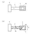
上記光導波路,受光素子を用い、図1(a),(b)に示す光センサを作製した。なお、固定部材は、合成樹脂製とした。
〔光センサ〕
上記実施例1と同様にして、図2(a),(b)に示す光センサを作製した。
〔光センサ〕
上記実施例1と同様にして、図3に示す光センサを作製した。
図5に示す従来の光センサを準備した。
上記実施例1~3および従来例の光センサにおける固定部材の寸法を測定した。その結果、実施例1の固定部材の幅Wは0.8mm、実施例2の固定部材の部分の厚みTは0.33mm、実施例3の固定部材の部分の厚みTは0.33mmであった。また、従来例の固定部材の部分の幅W1は1.6mm、厚みT1は0.53mmであった。
4 受光素子
Claims (2)
- 受光素子と、
線状の光導波路と
を備えている光センサであって、
上記受光素子に、上記線状の光導波路が光伝播可能に接続され、上記線状の光導波路の先端部が、光の入射部に形成されており、
機器に設置され、その機器に対する外部からの光を、上記入射部から入射して上記受光素子で受光し、その受光する光の状態を検知することを特徴とする光センサ。 - 上記光導波路の光入射部が固定される固定部材を備え、
上記受光素子が上記固定部材から離れて配置されている請求項1記載の光センサ。
Priority Applications (3)
| Application Number | Priority Date | Filing Date | Title |
|---|---|---|---|
| KR1020177001095A KR20170040191A (ko) | 2014-07-31 | 2015-07-17 | 광센서 |
| CN201580038508.3A CN106663702B (zh) | 2014-07-31 | 2015-07-17 | 光传感器 |
| US15/326,702 US10260939B2 (en) | 2014-07-31 | 2015-07-17 | Optical sensor having light entrance portion smaller than light-receiving element |
Applications Claiming Priority (2)
| Application Number | Priority Date | Filing Date | Title |
|---|---|---|---|
| JP2014-156330 | 2014-07-31 | ||
| JP2014156330A JP6369936B2 (ja) | 2014-07-31 | 2014-07-31 | 光センサ |
Publications (1)
| Publication Number | Publication Date |
|---|---|
| WO2016017444A1 true WO2016017444A1 (ja) | 2016-02-04 |
Family
ID=55217349
Family Applications (1)
| Application Number | Title | Priority Date | Filing Date |
|---|---|---|---|
| PCT/JP2015/070474 Ceased WO2016017444A1 (ja) | 2014-07-31 | 2015-07-17 | 光センサ |
Country Status (6)
| Country | Link |
|---|---|
| US (1) | US10260939B2 (ja) |
| JP (1) | JP6369936B2 (ja) |
| KR (1) | KR20170040191A (ja) |
| CN (1) | CN106663702B (ja) |
| TW (1) | TWI666936B (ja) |
| WO (1) | WO2016017444A1 (ja) |
Families Citing this family (3)
| Publication number | Priority date | Publication date | Assignee | Title |
|---|---|---|---|---|
| US11011355B2 (en) | 2017-05-12 | 2021-05-18 | Lam Research Corporation | Temperature-tuned substrate support for substrate processing systems |
| US10553179B2 (en) * | 2017-09-08 | 2020-02-04 | Apple Inc. | Electronic devices with ambient light sensors |
| WO2024238611A2 (en) * | 2023-05-16 | 2024-11-21 | Intuitive Surgical Operations, Inc. | Systems and methods for quantifying light intensity |
Citations (3)
| Publication number | Priority date | Publication date | Assignee | Title |
|---|---|---|---|---|
| JP2009128430A (ja) * | 2007-11-20 | 2009-06-11 | Nitto Denko Corp | 光導波路デバイスの製法およびそれによって得られる光導波路デバイス、並びにそれに用いられる光導波路接続構造 |
| JP2011064910A (ja) * | 2009-09-16 | 2011-03-31 | Nitto Denko Corp | 光電気混載モジュールおよびその製造方法 |
| JP2012208306A (ja) * | 2011-03-29 | 2012-10-25 | Nitto Denko Corp | 光電気混載基板およびその製法 |
Family Cites Families (13)
| Publication number | Priority date | Publication date | Assignee | Title |
|---|---|---|---|---|
| JPS49101638U (ja) * | 1972-12-20 | 1974-09-02 | ||
| JPS52135690A (en) * | 1976-05-10 | 1977-11-12 | Mitsubishi Electric Corp | Semiconductor element device |
| JPS5522713A (en) * | 1978-08-04 | 1980-02-18 | Fujitsu Ltd | Connector mechanism of photo semiconductor device |
| NL7908536A (nl) | 1979-11-23 | 1981-06-16 | Philips Nv | Omhulling voor een fotodiode. |
| JPS5687374U (ja) | 1979-12-06 | 1981-07-13 | ||
| JPS5691459U (ja) * | 1979-12-17 | 1981-07-21 | ||
| JPS56121272U (ja) * | 1980-02-15 | 1981-09-16 | ||
| JPS56121381U (ja) * | 1980-02-15 | 1981-09-16 | ||
| JPS6246370Y2 (ja) * | 1980-10-27 | 1987-12-14 | ||
| US4933545A (en) * | 1985-12-30 | 1990-06-12 | Metricor, Inc. | Optical pressure-sensing system using optical resonator cavity |
| JPH063594A (ja) * | 1992-06-18 | 1994-01-14 | Nikon Corp | コンフォーカルレーザ走査微分干渉顕微鏡 |
| JP6110673B2 (ja) | 2012-02-17 | 2017-04-05 | エスアイアイ・セミコンダクタ株式会社 | 光センサ装置 |
| JP6380973B2 (ja) * | 2014-06-16 | 2018-08-29 | 日東電工株式会社 | 光学式センサ |
-
2014
- 2014-07-31 JP JP2014156330A patent/JP6369936B2/ja not_active Expired - Fee Related
-
2015
- 2015-07-17 CN CN201580038508.3A patent/CN106663702B/zh not_active Expired - Fee Related
- 2015-07-17 US US15/326,702 patent/US10260939B2/en active Active
- 2015-07-17 KR KR1020177001095A patent/KR20170040191A/ko not_active Abandoned
- 2015-07-17 TW TW104123270A patent/TWI666936B/zh not_active IP Right Cessation
- 2015-07-17 WO PCT/JP2015/070474 patent/WO2016017444A1/ja not_active Ceased
Patent Citations (3)
| Publication number | Priority date | Publication date | Assignee | Title |
|---|---|---|---|---|
| JP2009128430A (ja) * | 2007-11-20 | 2009-06-11 | Nitto Denko Corp | 光導波路デバイスの製法およびそれによって得られる光導波路デバイス、並びにそれに用いられる光導波路接続構造 |
| JP2011064910A (ja) * | 2009-09-16 | 2011-03-31 | Nitto Denko Corp | 光電気混載モジュールおよびその製造方法 |
| JP2012208306A (ja) * | 2011-03-29 | 2012-10-25 | Nitto Denko Corp | 光電気混載基板およびその製法 |
Also Published As
| Publication number | Publication date |
|---|---|
| TW201611610A (zh) | 2016-03-16 |
| CN106663702B (zh) | 2020-08-07 |
| KR20170040191A (ko) | 2017-04-12 |
| JP6369936B2 (ja) | 2018-08-08 |
| CN106663702A (zh) | 2017-05-10 |
| TWI666936B (zh) | 2019-07-21 |
| JP2016033954A (ja) | 2016-03-10 |
| US20170211971A1 (en) | 2017-07-27 |
| US10260939B2 (en) | 2019-04-16 |
Similar Documents
| Publication | Publication Date | Title |
|---|---|---|
| US8064744B2 (en) | Planar waveguide lens design | |
| JP4910788B2 (ja) | 光モジュール及び光導波路の製造方法 | |
| JP2012168294A (ja) | 光コネクタの製法 | |
| JP6369936B2 (ja) | 光センサ | |
| JP6380973B2 (ja) | 光学式センサ | |
| US8111958B2 (en) | Optical waveguide with photoelectric conversion element and optical touch panel | |
| US20160238416A1 (en) | Position sensor production method, and position sensor produced by the method | |
| EP2975504A1 (en) | Position sensor | |
| WO2015025623A1 (ja) | 光電気混載モジュール | |
| JP6168602B2 (ja) | 光電気混載モジュール | |
| WO2016031601A1 (ja) | 位置センサ | |
| JP2016062159A (ja) | 位置センサ | |
| JP2016045771A (ja) | 位置センサ | |
| WO2016047448A1 (ja) | 位置センサ | |
| WO2016056393A1 (ja) | 位置センサ | |
| WO2016043047A1 (ja) | 位置センサ |
Legal Events
| Date | Code | Title | Description |
|---|---|---|---|
| 121 | Ep: the epo has been informed by wipo that ep was designated in this application |
Ref document number: 15828315 Country of ref document: EP Kind code of ref document: A1 |
|
| ENP | Entry into the national phase |
Ref document number: 20177001095 Country of ref document: KR Kind code of ref document: A |
|
| WWE | Wipo information: entry into national phase |
Ref document number: 15326702 Country of ref document: US |
|
| NENP | Non-entry into the national phase |
Ref country code: DE |
|
| 122 | Ep: pct application non-entry in european phase |
Ref document number: 15828315 Country of ref document: EP Kind code of ref document: A1 |