WO2016013059A1 - インダクタンス部品 - Google Patents
インダクタンス部品 Download PDFInfo
- Publication number
- WO2016013059A1 WO2016013059A1 PCT/JP2014/069346 JP2014069346W WO2016013059A1 WO 2016013059 A1 WO2016013059 A1 WO 2016013059A1 JP 2014069346 W JP2014069346 W JP 2014069346W WO 2016013059 A1 WO2016013059 A1 WO 2016013059A1
- Authority
- WO
- WIPO (PCT)
- Prior art keywords
- magnetic
- bias applying
- magnetic bias
- ferrite core
- applying members
- Prior art date
- Legal status (The legal status is an assumption and is not a legal conclusion. Google has not performed a legal analysis and makes no representation as to the accuracy of the status listed.)
- Ceased
Links
Images



Classifications
-
- H—ELECTRICITY
- H01—ELECTRIC ELEMENTS
- H01F—MAGNETS; INDUCTANCES; TRANSFORMERS; SELECTION OF MATERIALS FOR THEIR MAGNETIC PROPERTIES
- H01F17/00—Fixed inductances of the signal type
- H01F17/04—Fixed inductances of the signal type with magnetic core
Definitions
- the present invention relates to an inductance component.
- a choke coil used for a switching power supply for example, an alternating current is usually applied by being superimposed on a direct current.
- the ferrite core used for these choke coils is required to have good permeability characteristics that do not cause magnetic saturation with respect to this DC superposition.
- Ferrite cores and metal dust cores are used as magnetic cores for high frequencies.
- the ferrite core has a high initial permeability and a low saturation magnetic flux density
- the metal-based dust core has a feature derived from material properties such as a low initial permeability and a high saturation magnetic flux density. For this reason, metal-based dust cores are often used without a magnetic airspace due to the toroidal shape, etc.
- a magnetic air gap is formed in the middle leg of the E-type core to provide direct current superposition. Often avoids magnetic saturation.
- metal-based dust cores are expensive and expensive to manufacture.
- a magnetic bias applying member such as a permanent magnet is disposed in the gap provided in the magnetic path of the ferrite core to cancel the magnetic field due to DC superposition, that is, to apply a magnetic bias to the ferrite core. It has been proposed (see Patent Document 1). According to the magnetic bias method using the magnetic bias applying member, the available ⁇ B (magnetic flux density) region can be increased by applying the magnetic bias in the reverse direction using the magnetic bias applying member. .
- the present invention has been made in view of these points, and provides an inductance component having a ferrite core that can suppress core loss of the ferrite core while maintaining high DC superposition characteristics.
- the inductance component according to the present invention is: A ferrite core body having three or more gaps in the magnetic path; Three or more magnetic bias applying members disposed in the gap and providing a magnetic bias; With The magnetic bias applying member is disposed in each gap.
- the inductance component according to the present invention is: Comprising four or more magnetic bias applying members,
- the ferrite core body is provided with four or more gaps in the magnetic path,
- the magnetic bias applying member may be disposed in each gap.
- the gaps are evenly arranged;
- the distance between each member for applying a magnetic bias arranged in the gap may be the same.
- the gap may be provided line-symmetrically or point-symmetrically, and the magnetic bias applying member arranged in the gap may be arranged line-symmetrically or point-symmetrically.
- the number of the air gap and the magnetic bias applying member disposed in the air gap may be 10 or less.
- the magnetic bias applying member may be a permanent magnet.
- the inductance component of the present invention includes a ferrite core body in which three or more gaps are provided in a magnetic path, and three or more magnetic bias applying members that are disposed in the gap and provide a magnetic bias.
- a magnetic bias applying member is disposed in each gap. For this reason, the core loss of the ferrite core can be suppressed while maintaining high DC superposition characteristics.
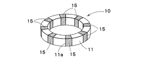
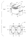
- FIG. 1A is a perspective view showing a ferrite core employed in the first embodiment of the present invention
- FIG. 1B shows an inductance component according to the first embodiment of the present invention. It is a perspective view.
- FIG. 2 is a perspective view showing a ferrite core employed in a modification of the first embodiment of the present invention.
- FIG. 3 is a perspective view showing a ferrite core employed in another modification of the first embodiment of the present invention.
- FIG. 4 is a graph showing the relationship between the number of installed magnetic bias applying members and the effective magnetic permeability in the first embodiment of the present invention.
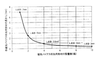
- FIG. 5 is a graph showing the relationship between the number of installed magnetic bias applying members and the length of each magnetic bias applying member in the first embodiment of the present invention.
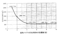
- FIG. 6 is a graph showing the relationship between the number of installed magnetic bias applying members and the core loss in the first embodiment of the present invention.
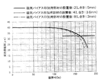
- FIG. 7 is a graph showing the DC superimposition characteristics in the first embodiment of the present invention.
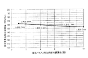
- FIG. 8 shows the relationship between the number of installed magnetic bias applying members and the DC superposition characteristics (the value of the magnetic field H when the effective permeability is reduced by 20% from the initial value) in the first embodiment of the present invention. It is the graph which showed.
- FIG. 9A is a perspective view showing an inductance component according to the second embodiment of the present invention
- FIG. 9B is a cross-sectional view taken along the line BB in FIG. 9A. It is a longitudinal cross-sectional view.
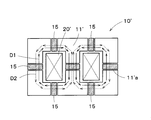
- FIG. 10 is a longitudinal sectional view showing the direction of a magnetic field generated by a current flowing through a conducting wire and the direction of a magnetic field generated by a magnetic bias applying member in an inductance component according to a second embodiment of the present invention. It is.
- FIG. 1 to FIG. 8 are diagrams for explaining the present embodiment.
- the inductance component includes a ferrite core 10 having a toroidal shape (ring shape) and a conductive wire 20 attached to the ferrite core 10.
- a magnetic field is generated in the ferrite core 10 so as to go around the ferrite core 10 once.
- the ferrite core 10 is formed with one closed magnetic path.
- the “DC superposition characteristic” means a characteristic that the ferrite core 10 is magnetically saturated when the DC superposition current becomes large, and as a result, the inductance value decreases. Therefore, “high DC superposition characteristics” means that the ferrite core 10 is hard to be magnetically saturated even when the DC superposition current increases.
- the ferrite core 10 in the present embodiment has an inner diameter of 20 mm to 26 mm (for example, 23 mm), an outer diameter of 33 mm to 39 mm (for example, 36 mm), and a height of 12 mm to 18 mm (for example, 15 mm). ing.
- the conductive wire 20 made of, for example, copper is attached to the ferrite core 10 by being spirally wound around the ferrite core 10.
- the ferrite core 10 in the present embodiment is provided in the ferrite core body 11 in which three or more gaps 11a (four gaps 11a in the embodiment shown in FIG. 1) are provided in the magnetic path, and in each gap 11a. And three or more magnetic bias applying members 15 for applying a magnetic bias.
- the air gap 11a is provided to prevent magnetic saturation.
- the magnetic bias applying member 15 is made of a material different from that of the ferrite core body 11.
- the ferrite core body 11 for example, a powder formed by compressing and molding a powder containing iron oxide as a main component and then firing the powder can be used. You may use what was formed by compression-molding material powder and a binder.
- the soft magnetic material powder an appropriate one such as FeSiCr powder, FeSi powder, carbonyl iron powder, sendust powder, permalloy powder or amorphous material powder can be used.
- the size of the ferrite core body 11 can be adjusted as appropriate.
- the magnetic bias applying member 15 is formed, for example, by molding a composite magnetic material containing hard magnetic material powder, soft magnetic material powder and a binder into a flat plate shape. Specifically, the composite magnetic material is formed by compression molding (for example, press molding). The magnetic bias applying member 15 is a bonded magnet made of a permanent magnet, for example.
- the composite magnetic material may contain alumina (Al 2 O 3 ) powder, aluminum nitride (AlN) powder, or the like as an additive for heat dissipation.
- the ratio of the hard magnetic material powder to the total of the hard magnetic material powder and the soft magnetic material powder is in the range of 20 wt% to 90 wt%, preferably in the range of 50 wt% to 90 wt%. For example, 80 wt%.
- the average particle size of the hard magnetic material powder is in the range of several tens of ⁇ m to several hundreds of ⁇ m, for example, about 150 ⁇ m.
- the hard magnetic material powder for example, samarium cobalt (SmCo) powder can be used, but any magnetic material powder having a high coercive force may be used. For this reason, for example, hard magnetic material powder such as samarium iron nitrogen (SmFeN) powder, neodymium iron boron (NdFeB) powder, or ferrite powder can be used.
- the ratio of the hard magnetic material powder to the total of the hard magnetic material powder and the soft magnetic material powder when the ratio of the hard magnetic material powder to the total of the hard magnetic material powder and the soft magnetic material powder is less than 20 wt%, the ratio of the hard magnetic material powder is too small, so that the magnetic bias A sufficient magnetic force cannot be obtained as the application member 15.
- the ratio of the hard magnetic material powder to the total of the hard magnetic material powder and the soft magnetic material powder exceeds 90 wt%, the ratio of the hard magnetic material powder is increased, so that for other conventional magnetic bias application As in the case of the member 15, when trying to manufacture a relatively thin magnetic bias applying member 15, it becomes difficult to manufacture the magnetic bias applying member 15 having a small thickness variation.
- the ratio of the soft magnetic material powder to the total of the hard magnetic material powder and the soft magnetic material powder is in the range of 10 wt% to 80 wt%, preferably in the range of 10 wt% to 50 wt%. For example, 20 wt%.
- the soft magnetic material powder a soft magnetic material powder whose surface is covered with a silica film (insulated) can be used.
- the average particle diameter of the soft magnetic material powder is in the range of several tens of ⁇ m to several hundreds of ⁇ m, for example, about 150 ⁇ m.
- FeSiCr powder can be used, but any magnetic material powder having a high magnetic permeability may be used. For this reason, for example, FeSi powder, ferrite powder, carbonyl iron powder, sendust powder, permalloy powder, or amorphous material powder can be used.
- the ratio of the soft magnetic material powder to the total of the hard magnetic material powder and the soft magnetic material powder is less than 10 wt%, the ratio of the hard magnetic material powder is increased, and thus other conventional magnetic materials are used.
- the bias applying member 15 when trying to manufacture a relatively thin magnetic bias applying member 15, it becomes difficult to manufacture the magnetic bias applying member 15 having a small thickness variation.
- the ratio of the soft magnetic material powder to the total of the hard magnetic material powder and the soft magnetic material powder exceeds 80 wt%, the ratio of the hard magnetic material powder is too small, so that the magnetic bias applying member 15 is sufficient. Cannot obtain a strong magnetic force.
- the binder in the composite magnetic material is made of a polymer and has a function of joining the hard magnetic material powder and the soft magnetic material powder.
- the binder content in the composite magnetic material also varies depending on the method of manufacturing the magnetic bias applying member 15. For example, when the magnetic bias applying member 15 is manufactured by press molding a composite magnetic material, it is preferably in the range of 1 wt% to 5 wt%, for example 3 wt%.
- a thermosetting resin or a thermoplastic resin can be used. More specifically, for example, an epoxy resin, a polyimide resin, a polyamideimide resin, a silicone resin, a phenol resin, or the like can be used as the binder.
- the magnetic bias applying member 15 is formed by press molding the composite magnetic material
- the binder content in the composite magnetic material is less than 1 wt%, the ratio of the binder is too small and hard magnetic It is difficult to join between the material powder and the soft magnetic material powder.
- the content of the binder in the composite magnetic material exceeds 5 wt%, the content of the hard magnetic material powder and the soft magnetic material powder is reduced, so that the relative permeability of the magnetic bias applying member 15 is reduced,
- the magnetic flux density range ⁇ B that does not reach the saturation magnetic flux density may be smaller than other conventional ferrite core bodies 11.
- the magnetic bias applying member 15 is arranged so that the direction of the magnetic field generated in the magnetic bias applying member 15 is opposite to the direction of the magnetic field generated when a current flows through the conductive wire 20 (that is, on the conductive wire 20).
- the magnetic bias is applied in the direction opposite to the magnetic field generated by the flow of current.
- the gaps 11a are evenly arranged.
- the magnetic bias applying members 15 arranged in the gap 11a are evenly arranged, and the distances between the magnetic bias applying members 15 are the same.
- the gap 11a is provided with line symmetry and point symmetry.
- the magnetic bias applying members 15 arranged in the gap 11a are arranged in line symmetry and point symmetry.
- a ferrite core main body 11 having four air gaps 11a provided in a magnetic path, four magnetic bias applying members 15 disposed in the air gaps 11a and providing a magnetic bias
- the present invention is not limited to this. That is, the ferrite core 10 including the ferrite core body 11 provided with three gaps 11a in the magnetic path and the three magnetic bias applying members 15 disposed in the gaps 11a and applying a magnetic bias is provided. It may be used. Also, a ferrite core comprising a ferrite core body 11 having five or more air gaps 11a provided in the magnetic path, and five or more magnetic bias applying members 15 disposed in the air gaps 11a and applying a magnetic bias. 10 may be used.
- the ferrite core body 11 is provided with eight gaps 11 a in the magnetic path, and eight magnetic bias applying members 15 that are disposed in the gaps 11 a and provide a magnetic bias are provided.
- a ferrite core 10 is shown.
- a ferrite core main body 11 having 10 gaps 11 a provided in a magnetic path, and 10 magnetic bias applying members 15 that are arranged in the gaps 11 a and provide a magnetic bias are provided.
- a ferrite core 10 is shown.
- the gaps 11a are evenly arranged.
- the magnetic bias applying members 15 arranged in the gap 11a are evenly arranged, and the distances between the magnetic bias applying members 15 are the same.
- the air gap 11a is provided with line symmetry and point symmetry.
- the magnetic bias applying members 15 arranged in the gap 11a are arranged in line symmetry and point symmetry.
- the gap 11a is not necessarily provided in line symmetry and point symmetry.
- the magnetic bias applying member 15 is arranged line-symmetrically but may not be arranged point-symmetrically.
- the magnetic bias applying member 15 is arranged point-symmetrically but line-symmetrically. It may not be arranged.
- the magnetic bias applying member 15 is not arranged line-symmetrically and may not be arranged point-symmetrically.
- a ferrite core body 11 having four magnetic saturation prevention gaps 11a formed in a magnetic path is prepared.
- four gaps 11a may be formed after forming a ring-shaped ferrite core body part having no gap 11a, or four ferrite core body parts in consideration of the gap 11a in advance. And four gaps 11a may be formed by combining four ferrite core body parts.
- the ferrite core 10 is manufactured by disposing the magnetic bias applying member 15 in the gap 11 a in the ferrite core body 11.
- the inductance component according to the present embodiment is manufactured by attaching the conductive wire 20 to the ferrite core 10 thus manufactured (see FIG. 1B).
- a hard magnetic material powder, a soft magnetic material powder and a binder are uniformly kneaded at a predetermined ratio and then granulated to produce a composite magnetic material.
- the composite magnetic material is dried to volatilize the solvent component in the binder.
- the composite magnetic material is sieved, and only the composite magnetic material having a particle size suitable for molding (within a range of several tens to several hundreds of ⁇ m) is recovered.
- a compact is produced by molding the composite magnetic material into a flat plate shape. Specifically, a composite magnetic material is deposited in a molding space and press-molded to produce a molded body.
- the pressing pressure in the press molding is, for example, in the range of 3 ton / cm 2 to 10 ton / cm 2 .
- the temperature at the time of press molding shall be room temperature.
- the molded body is heated to cure the binder.
- the temperature and time which heat a molded object are based also on the kind of binder, it shall be 1 hour at 150 degreeC, for example.
- the molded body in which the binder is cured is magnetized to obtain a magnetic bias applying member 15.
- the molded body obtained by curing the binder is magnetized using a pulse magnetizing apparatus. In this way, the magnetic bias applying member 15 can be manufactured.
- FIG. 4 is a graph showing the relationship between the number of installed magnetic bias applying members 15 and the effective magnetic permeability.
- FIG. 4 shows an aspect in which a permanent magnet is used as the magnetic bias applying member 15 and the total length of the permanent magnet is 5 mm.
- the case where the number of the magnetic bias applying members 15 is 1, 2, 4, (see FIG. 1), 8 (see FIG. 2), and 10 (see FIG. 3) is plotted. Yes.
- the length of each permanent magnet when the number of magnetic bias applying members 15 is 1, 2, 4, (see FIG. 1), 8 (see FIG. 2), and 10 (see FIG. 3).
- the lengths are 5 mm, 2.5 mm, 1.25 mm, 0.625 mm, and 0.5 mm, respectively.
- FIG. 4 shows an aspect in which a permanent magnet is used as the magnetic bias applying member 15 and the total length of the permanent magnet is 5 mm.
- the number of the magnetic bias applying members 15 is 1, 2, 4, (see FIG. 1), 8 (see FIG. 2), and 10 (see FIG.
- the effective magnetic permeability is increased by setting the number of the magnetic bias applying members 15 to 3 or more as compared with the case where the number of the magnetic bias applying members 15 is one. Can be greatly reduced. Furthermore, by making the number of the magnetic bias applying members 15 four or more, the effective magnetic permeability can be reduced to half or less as compared with the case where the number of the magnetic bias applying members 15 is one. The effective magnetic permeability can be reduced more greatly. More specifically, when the number of magnetic bias applying members 15 is one, the effective magnetic permeability, which is about 70 ⁇ e, is 30 ⁇ e or less by setting the number of magnetic bias applying members 15 to four or more. can do.
- the effective magnetic permeability cannot be reduced so efficiently, and the effect obtained when the number of the magnetic bias applying members 15 is 10 is effective. There is no significant difference between the magnetic permeability and the effective magnetic permeability when the number of magnetic bias applying members 15 is increased beyond that (for example, when the number of magnetic bias applying members 15 is 11).
- FIG. 5 shows the relationship between the number of installed magnetic bias applying members 15 and the length of each magnetic bias applying member 15.
- FIG. 5 shows the total length of the permanent magnet when a permanent magnet is used as the magnetic bias applying member 15 and the effective permeability is 40 ⁇ e.
- the number of magnetic bias applying members 15 is one, two, four (see FIG. 1), eight (see FIG. 2), and ten (see FIG. 3). The case is plotted.
- the total number of permanent magnets when the number of magnetic bias applying members 15 is 1, 2, 4, (see FIG. 1), 8 (see FIG. 2), and 10 (see FIG. 3).
- the lengths are about 7 mm, about 5 mm, about 3.6 mm, about 3 mm, and about 3 mm, respectively.
- the total length of the permanent magnets is greatly shortened by setting the number of the magnetic bias applying members 15 to three or more. be able to. Furthermore, the total length of the permanent magnets can be dramatically shortened by setting the number of the magnetic bias applying members 15 to four or more. Specifically, by setting the number of the magnetic bias applying members 15 to 4 or more, the total length of the permanent magnets is reduced as compared with the case where the number of the magnetic bias applying members 15 is one. It can be less than half.
- the total length of the permanent magnets which is about 7 mm
- the number of the magnetic bias applying members 15 is four or more. About 3.6 mm or less.
- the total length of the permanent magnets and the total length of the permanent magnets when the number of the magnetic bias applying members 15 is 10 are both about 3 mm.
- the ferrite core 10 in the present embodiment has an inner diameter of 20 mm to 26 mm (for example, 23 mm), an outer diameter of 33 mm to 39 mm (for example, 36 mm), and a height of 12 mm to 18 mm (for example, 15 mm). ).
- the inner diameter is 23 mm
- the outer diameter is 36 mm
- the height is 15 mm
- the number of the magnetic bias applying members 15 is one, the size of the gap 11a to be formed is large.
- FIG. 6 shows the relationship between the number of installed magnetic bias applying members 15 and the core loss.
- FIG. 6 shows the core loss when a permanent magnet is used as the magnetic bias applying member 15 and the effective permeability is 40 ⁇ e. 6, as in FIG. 4, the number of magnetic bias applying members 15 is one, two, four (see FIG. 1), eight (see FIG. 2), and ten (see FIG. 3). The case is plotted.
- the core loss can be greatly reduced by setting the number of the magnetic bias applying members 15 to three or more.
- the core loss can be dramatically reduced by setting the number of the magnetic bias applying members 15 to four or more.
- the core loss is reduced to about a quarter compared with the case where the number of the magnetic bias applying members 15 is one. be able to. More specifically, when the number of magnetic bias applying members 15 is one, the core loss is about 2500 mW / cm 3 , and when the number of magnetic bias applying members 15 is four or more, it is about 600 mW. / Cm 3 or less. On the other hand, even if the number of magnetic bias applying members 15 is further increased from eight, the core loss cannot be reduced so efficiently, and the core loss when the number of magnetic bias applying members 15 is eight; When the number of the magnetic bias applying members 15 is 10, the core loss of the permanent magnet is about 500 mW / cm 3 .
- FIG. 7 is a graph showing the DC superposition characteristics, and the magnetic field H and the effective when the number of magnetic bias applying members 15 is 2, 4, (see FIG. 1) and 8 (see FIG. 2). It is the graph which showed the relationship with the magnetic permeability.
- FIG. 8 shows the relationship between the number of installed magnetic bias applying members 15 and the DC superposition characteristics (the value of the magnetic field H when the effective permeability is reduced by 20% from the initial value).
- FIG. 8 shows the DC superposition characteristics (the value of the magnetic field H when the effective permeability is reduced by 20% from the initial value) when a permanent magnet is used as the magnetic bias applying member 15 and the effective permeability is 40 ⁇ e. ing. 8, as in FIG. 4, the number of magnetic bias applying members 15 is one, two, four (see FIG.
- the inductance component according to the present embodiment is arranged in the ferrite core body 11 in which three or more (preferably four or more) gaps 11a are provided in the magnetic path, and is disposed in the gap 11a. And 3 or more (preferably 4 or more) magnetic bias applying members 15 to be provided. A magnetic bias applying member 15 is disposed in each gap 11a.
- the core loss of the ferrite core 10 can be suppressed while maintaining high DC superposition characteristics.
- the gaps 11a are evenly arranged in the ferrite core body 11, the magnetic bias applying members 15 arranged in the gaps 11a are evenly arranged, and the magnetic bias applying members 15 are arranged.
- the ferrite core body 11 is provided with the gap 11a in line symmetry and / or point symmetry, and the magnetic bias applying member 15 arranged in the gap 11a is arranged in line symmetry and / or point symmetry.
- the core loss is substantially reduced to a lower limit (in FIG. 6, about 500 mW / cm 3). ) Can be lowered. For this reason, when the aspect which makes the number of the members 15 for magnetic bias application 15 6 or more is employ
- the magnitude of the core loss is approximately the same when the number of the magnetic bias applying members 15 is eight and when the number is ten.
- the number of the gaps 11a provided in the ferrite core main body 11 and the magnetic bias applying members 15 arranged in the gap 11a may be 10 or less.
- the ferrite core body 11 having a toroidal shape is used.
- the shape is not limited to such a shape.
- the ferrite core 10 ′ of the second embodiment is a ferrite core body 11 ′ formed by overlapping two E-type cores as shown in FIGS. 9 (a), (b) and FIG. 10. It has.
- a magnetic path is formed as shown in FIG.
- the other configurations are substantially the same as those in the first embodiment.
- the same parts as those in the first embodiment are denoted by the same reference numerals, and detailed description thereof is omitted.
- the “solid line” indicated by reference sign D1 indicates the direction of the magnetic field generated by the current flowing through the conductor 20 ′
- the “broken line” indicated by reference sign D2 indicates the direction of the magnetic field by the magnetic bias applying member 15. Show.
- the inductance component is disposed in the ferrite core body 11 ′ in which three or more (preferably four or more) gaps 11′a are provided in the magnetic path, and in the gap 11′a. And three or more (preferably four or more) magnetic bias applying members 15 for applying a magnetic bias.
- a magnetic bias applying member 15 is disposed in each gap 11'a. For this reason, the core loss of the ferrite core 10 ′ can be suppressed while maintaining high DC superposition characteristics.
- the gaps 11′a are evenly arranged in the ferrite core body 11 ′, the magnetic bias applying members 15 arranged in the gaps 11′a are arranged uniformly, and the magnetic
- the ferrite core body 11 ' is provided with the gap 11'a in line symmetry and / or point symmetry, and the magnetic bias applying member 15 disposed in the gap 11'a is line symmetrical and / or Alternatively, the core loss can be suppressed in a well-balanced manner by adopting an aspect of being arranged point-symmetrically. In addition, it is possible to maintain high DC superposition characteristics more stably.
Landscapes
- Engineering & Computer Science (AREA)
- Power Engineering (AREA)
- Microelectronics & Electronic Packaging (AREA)
- Coils Or Transformers For Communication (AREA)
Abstract
インダクタンス部品は、磁路に3個以上の空隙11aが設けられたフェライトコア本体11と、空隙11a内に配置され、磁気バイアスを与える3個以上の磁気バイアス印加用部材15と、を備えている。各空隙11a内に磁気バイアス印加用部材15が配置される。
Description
本発明はインダクタンス部品に関する。
例えばスイッチング電源等に用いられるチョークコイルにおいては、通常、交流が直流に重畳して印加される。このため、これらチョークコイルに用いるフェライトコアは、この直流重畳に対して磁気飽和しない透磁率特性が良好であることが求められている。
高周波用の磁気コアとしてはフェライトコアや金属系圧粉コアが使用されている。フェライトコアは初透磁率が高く飽和磁束密度が小さくなっているのに対して、金属系圧粉コアは初透磁率が低く飽和磁束密度が高いという材料物性に由来した特徴がある。このため、金属系圧粉コアはトロイダル形状等で磁気空域を設けないで用いられることが多く、他方、フェライトコアの場合には、例えばE型コアの中足に磁気空隙を形成して直流重畳により磁気飽和することを避けることが多い。
また、金属系圧粉コアは価格が高く製造コストがかかってしまう。この点、フェライトコアを用いた場合には価格を抑えることができるものの、直流重畳電流の特性が劣化するという問題が発生する。この問題を解決するために、フェライトコアの磁路に設けた空隙に永久磁石等の磁気バイアス印加用部材を配置し、直流重畳による磁界を打ち消すこと、すなわち、フェライトコアに磁気バイアスを与えることが提案されている(特許文献1参照)。この磁気バイアス印加用部材を用いた磁気バイアス方法によれば、磁気バイアス印加用部材を利用して逆方向に磁気バイアスを印加することにより、利用可能なΔB(磁束密度)領域を増やすことができる。通常はコア材のBH特性の第1象限しか利用しない回路方式において、磁気バイアス印加により第3象限まで利用することができ、理論的にはΔBを2倍まで増加させることができるためである。しかしながら、このように磁気バイアス印加用部材を配置することでフェライトコアのコアロスが増大してしまうという問題が発生する。
本発明は、このような点を鑑みてなされたものであり、高い直流重畳特性を維持しつつフェライトコアのコアロスを抑えることができる、フェライトコアを有するインダクタンス部品を提供する。
本発明によるインダクタンス部品は、
磁路に3個以上の空隙が設けられたフェライトコア本体と、
前記空隙内に配置され、磁気バイアスを与える3個以上の磁気バイアス印加用部材と、
を備え、
各空隙内に前記磁気バイアス印加用部材が配置される。
磁路に3個以上の空隙が設けられたフェライトコア本体と、
前記空隙内に配置され、磁気バイアスを与える3個以上の磁気バイアス印加用部材と、
を備え、
各空隙内に前記磁気バイアス印加用部材が配置される。
本発明によるインダクタンス部品は、
4個以上の前記磁気バイアス印加用部材を備え、
前記フェライトコア本体には、前記磁路に4個以上の空隙が設けられ、
各空隙内に前記磁気バイアス印加用部材が配置されてもよい。
4個以上の前記磁気バイアス印加用部材を備え、
前記フェライトコア本体には、前記磁路に4個以上の空隙が設けられ、
各空隙内に前記磁気バイアス印加用部材が配置されてもよい。
本発明によるインダクタンス部品において、
前記空隙は均等に配置され、
前記空隙内に配置された各磁気バイアス印加用部材の間の距離は同一になっていてもよい。
前記空隙は均等に配置され、
前記空隙内に配置された各磁気バイアス印加用部材の間の距離は同一になっていてもよい。
本発明によるインダクタンス部品において、
前記空隙は線対称又は点対称に設けられ
前記空隙内に配置された前記磁気バイアス印加用部材は線対称又は点対称に配置されていてもよい。
前記空隙は線対称又は点対称に設けられ
前記空隙内に配置された前記磁気バイアス印加用部材は線対称又は点対称に配置されていてもよい。
本発明によるインダクタンス部品において、
前記空隙及び当該空隙内に配置された前記磁気バイアス印加用部材の個数は10個以下であってもよい。
前記空隙及び当該空隙内に配置された前記磁気バイアス印加用部材の個数は10個以下であってもよい。
本発明によるインダクタンス部品において、
前記磁気バイアス印加用部材は永久磁石であってもよい。
前記磁気バイアス印加用部材は永久磁石であってもよい。
本発明のインダクタンス部品は、磁路に3個以上の空隙が設けられたフェライトコア本体と、空隙内に配置され、磁気バイアスを与える3個以上の磁気バイアス印加用部材と、を備えている。そして、各空隙内に磁気バイアス印加用部材が配置されている。このため、高い直流重畳特性を維持しつつ、フェライトコアのコアロスを抑えることができる。
第1の実施の形態
《構成》
以下、本発明に係るインダクタンス部品の第1の実施の形態について、図面を参照して説明する。ここで、図1乃至図8は本実施の形態を説明するための図である。
《構成》
以下、本発明に係るインダクタンス部品の第1の実施の形態について、図面を参照して説明する。ここで、図1乃至図8は本実施の形態を説明するための図である。
図1(b)に示すように、本実施の形態によるインダクタンス部品は、トロイダル形状(リング形状)からなるフェライトコア10と、フェライトコア10に装着された導線20とを備えている。導線20に電流が流れると、フェライトコア10には、フェライトコア10を1周するように磁界が発生する。そして、このフェライトコア10には1個の閉じた磁路が形成される。なお、本実施の形態において、「直流重畳特性」とは、直流重畳電流が大きくなったときにフェライトコア10が磁気飽和し、その結果、インダクタンス値が低下する特性をいう。したがって、「高い直流重畳特性」とは、直流重畳電流が大きくなったときでもフェライトコア10が磁気飽和し難いことを意味している。
ちなみに、本実施の形態におけるフェライトコア10は、一例として、内径が20mm~26mm(例えば23mm)となり、外径が33mm~39mm(例えば36mm)となり、高さが12mm~18mm(例えば15mm)となっている。
本実施の形態では、例えば銅からなる導線20が、フェライトコア10を中心にらせん状に巻回されることでフェライトコア10に装着されている。
本実施の形態におけるフェライトコア10は、磁路に3個以上の空隙11a(図1に示す態様では4個の空隙11a)が設けられたフェライトコア本体11と、各空隙11a内に設けられ、磁気バイアスを与える3個以上の磁気バイアス印加用部材15とを有している。空隙11aは磁気飽和を防止するために設けられている。また、磁気バイアス印加用部材15は、フェライトコア本体11とは異なる材料からなっている。
フェライトコア本体11としては、例えば、酸化鉄を主成分とした粉末を圧縮して成形した後に、焼成したセラミック状のフェライトから形成されたものを用いることができるが、別の例として、軟磁性材料粉末とバインダーとを圧縮成形することにより形成されたものを用いてもよい。軟磁性材料粉末としては、FeSiCr粉末、FeSi粉末、カルボニル鉄粉末、センダスト粉末、パーマロイ粉末又はアモルファス材粉末等、適宜のものを用いることができる。フェライトコア本体11の大きさは適宜調整することができる。
磁気バイアス印加用部材15は、例えば、硬磁性材料粉末、軟磁性材料粉末及びバインダーを含有する複合磁性材料を平板状に成形することにより形成されている。具体的には、複合磁性材料を圧縮成形(例えば押圧成形)することにより形成されたものである。磁気バイアス印加用部材15は、例えば永久磁石からなるボンド磁石である。なお、複合磁性材料には、放熱のための添加剤としてアルミナ(Al2O3)粉末や窒化アルミニウム(AlN)粉末等が含まれていてもよい。
また、複合磁性材料においては、硬磁性材料粉末及び軟磁性材料粉末を合計したものに対する硬磁性材料粉末の割合が20wt%~90wt%の範囲内にあり、好ましくは、50wt%~90wt%の範囲内にあり、例えば80wt%である。硬磁性材料粉末の平均粒径は、数十μm~数百μmの範囲内にあり、例えば、150μm程度である。硬磁性材料粉末として、例えばサマリウムコバルト(SmCo)粉末を用いることができるが、保磁力の大きい性質を有する磁性材料粉末であればよい。このため、例えば、サマリウム鉄窒素(SmFeN)粉末、ネオジム鉄ボロン(NdFeB)粉末又はフェライト粉末等の硬磁性材料粉末を用いることができる。
なお、複合磁性材料においては、硬磁性材料粉末及び軟磁性材料粉末を合計したものに対する硬磁性材料粉末の割合が20wt%未満の場合には、硬磁性材料粉末の割合が小さすぎるため、磁気バイアス印加用部材15として十分な磁力を得ることができない。他方、硬磁性材料粉末及び軟磁性材料粉末を合計したものに対する硬磁性材料粉末の割合が90wt%を超える場合には、硬磁性材料粉末の割合が大きくなるため、他の従来の磁気バイアス印加用部材15の場合と同様、比較的薄い磁気バイアス印加用部材15を製造しようとした場合、厚さばらつきの小さい磁気バイアス印加用部材15を製造することが困難となる。
また、複合磁性材料においては、硬磁性材料粉末及び軟磁性材料粉末を合計したものに対する軟磁性材料粉末の割合が10wt%~80wt%の範囲内にあり、好ましくは、10wt%~50wt%の範囲内にあり、例えば、20wt%である。軟磁性材料粉末としては、表面がシリカ膜で覆われた(絶縁処理が施された)軟磁性材料粉末を用いることができる。軟磁性材料粉末の平均粒径は、数十μm~数百μmの範囲内にあり、例えば150μm程度である。軟磁性材料粉末としては、例えばFeSiCr粉末を用いることができるが、透磁率が大きい性質を有する磁性材料粉末であればよい。このため、例えば、FeSi粉末、フェライト粉末、カルボニル鉄粉末、センダスト粉末、パーマロイ粉末又はアモルファス材粉末等を用いることもできる。
複合磁性材料において、硬磁性材料粉末及び軟磁性材料粉末を合計したものに対する軟磁性材料粉末の割合が10wt%未満の場合には、硬磁性材料粉末の割合が大きくなるため、他の従来の磁気バイアス印加用部材15の場合と同様、比較的薄い磁気バイアス印加用部材15を製造しようとした場合、厚さばらつきの小さい磁気バイアス印加用部材15を製造することが困難となる。また、硬磁性材料粉末及び軟磁性材料粉末を合計したものに対する軟磁性材料粉末の割合が80wt%を超える場合には、硬磁性材料粉末の割合が小さすぎるため、磁気バイアス印加用部材15として十分な磁力を得ることができない。
複合磁性材料におけるバインダーは、ポリマーからなり、硬磁性材料粉末及び軟磁性材料粉末を接合する機能を有する。複合磁性材料におけるバインダーの含有量は、磁気バイアス印加用部材15の製造方法によっても異なる。例えば、複合磁性材料を押圧成形することによって磁気バイアス印加用部材15を製造する場合には、1wt%~5wt%の範囲内にあることが好ましく、例えば3wt%である。バインダーとして、熱硬化性樹脂又は熱可塑性樹脂を用いることができる。より具体的には、バインダーとして、例えば、エポキシ樹脂、ポリイミド樹脂、ポリアミドイミド樹脂、シリコーン樹脂、フェノール樹脂等を用いることができる。
なお、複合磁性材料を押圧成形することによって磁気バイアス印加用部材15を形成する場合において、複合磁性材料におけるバインダーの含有量が1wt%未満である場合には、バインダーの割合が小さすぎて硬磁性材料粉末及び軟磁性材料粉末の間を接合することが難しい。また、複合磁性材料におけるバインダーの含有量が5wt%を超える場合には、硬磁性材料粉末及び軟磁性材料粉末の含有量が少なくなるため、磁気バイアス印加用部材15の比透磁率が低くなり、飽和磁束密度に達しない磁束密度の範囲△Bが他の従来のフェライトコア本体11よりも小さくなるおそれがある。
磁気バイアス印加用部材15は、磁気バイアス印加用部材15内で発生する磁界の向きが、導線20に電流が流れることによって発生する磁界の向きとは逆向きになるように(すなわち、導線20に電流が流れることによって発生する磁界とは逆方向に磁気バイアスを印加するように)配置されている。
図1(a)(b)に示すように、本実施の形態では、空隙11aが均等に配置されている。この結果、空隙11a内に配置された各磁気バイアス印加用部材15は均等に配置され、各磁気バイアス印加用部材15の間の距離は同一になっている。
また、図1(a)(b)に示す態様では、空隙11aは線対称及び点対称に設けられている。この結果、空隙11a内に配置された磁気バイアス印加用部材15は線対称及び点対称に配置されている。
[変形例]
図1(a)(b)では、磁路に4個の空隙11aが設けられたフェライトコア本体11と、各空隙11a内に配置され、磁気バイアスを与える4個の磁気バイアス印加用部材15と、を備えたフェライトコア10を示しているが、これに限られることはない。つまり、磁路に3個の空隙11aが設けられたフェライトコア本体11と、各空隙11a内に配置され、磁気バイアスを与える3個の磁気バイアス印加用部材15と、を備えたフェライトコア10を用いてもよい。また、磁路に5つ以上の空隙11aが設けられたフェライトコア本体11と、各空隙11a内に配置され、磁気バイアスを与える5つ以上の磁気バイアス印加用部材15と、を備えたフェライトコア10を用いてもよい。
図1(a)(b)では、磁路に4個の空隙11aが設けられたフェライトコア本体11と、各空隙11a内に配置され、磁気バイアスを与える4個の磁気バイアス印加用部材15と、を備えたフェライトコア10を示しているが、これに限られることはない。つまり、磁路に3個の空隙11aが設けられたフェライトコア本体11と、各空隙11a内に配置され、磁気バイアスを与える3個の磁気バイアス印加用部材15と、を備えたフェライトコア10を用いてもよい。また、磁路に5つ以上の空隙11aが設けられたフェライトコア本体11と、各空隙11a内に配置され、磁気バイアスを与える5つ以上の磁気バイアス印加用部材15と、を備えたフェライトコア10を用いてもよい。
図2に示す態様では、磁路に8個の空隙11aが設けられたフェライトコア本体11と、各空隙11a内に配置され、磁気バイアスを与える8個の磁気バイアス印加用部材15と、を備えたフェライトコア10が示されている。
図3に示す態様では、磁路に10個の空隙11aが設けられたフェライトコア本体11と、各空隙11a内に配置され、磁気バイアスを与える10個の磁気バイアス印加用部材15と、を備えたフェライトコア10が示されている。
図2及び図3に示す態様でも、空隙11aが均等に配置されている。この結果、空隙11a内に配置された各磁気バイアス印加用部材15は均等に配置され、各磁気バイアス印加用部材15の間の距離は同一になっている。なお、これはあくまでも一例であり、各磁気バイアス印加用部材15が均等に配置され、各磁気バイアス印加用部材15の間の距離が同一になっている必要は必ずしもない。つまり、各磁気バイアス印加用部材15が均等に配置されていなくてもよく、各磁気バイアス印加用部材15の間の距離が異なっていてもよい。
また、図2及び図3に示す態様でも、空隙11aは線対称及び点対称に設けられている。この結果、空隙11a内に配置された磁気バイアス印加用部材15は線対称及び点対称に配置されている。なお、これもあくまでも一例であり、空隙11aは線対称及び点対称に設けられている必要は必ずしもない。例えば、磁気バイアス印加用部材15は線対称に配置されているが点対称に配置されていなくてもよいし、逆に、磁気バイアス印加用部材15は点対称に配置されているが線対称に配置されていなくてもよい。また、磁気バイアス印加用部材15は線対称に配置されておらず、かつ、点対称にも配置されていなくてもよい。
《方法》
次に、本実施の形態によるインダクタンス部品の製造方法の一例について説明する。なお、以下では、磁気バイアス印加用部材15が4個設けられた態様を例に取って説明する。
次に、本実施の形態によるインダクタンス部品の製造方法の一例について説明する。なお、以下では、磁気バイアス印加用部材15が4個設けられた態様を例に取って説明する。
まず、磁路に4個の磁気飽和防止用の空隙11aが形成されたフェライトコア本体11が準備される。なお、フェライトコア本体11においては、空隙11aのないリング形状のフェライトコア本体部品を形成した後に4個の空隙11aを形成してもよいし、予め空隙11aを考慮した4個のフェライトコア本体部品を準備し、4個のフェライトコア本体部品を組み合わせることで4個の空隙11aが形成されるようにしてもよい。
次に、磁気バイアス印加用部材15をフェライトコア本体11における空隙11aに配設することでフェライトコア10を作製する。このように作製されたフェライトコア10に導線20を装着することで本実施の形態によるインダクタンス部品が製造される(図1(b)参照)。
次に、上述した磁気バイアス印加用部材15を製造する方法の一例について説明する。
まず、硬磁性材料粉末、軟磁性材料粉末及びバインダーを所定の割合で均一に混錬した後に造粒し複合磁性材料を作製する。次に、複合磁性材料をバインダー中の溶媒成分を揮発させるために乾燥させる。次に、複合磁性材料をふるいにかけ、成形に適した粒度(数十μm~数百μmの範囲内)の複合磁性材料のみを回収する。
次に、複合磁性材料を平板状に成形することにより成形体を作製する。具体的には、複合磁性材料を成形空間に堆積させて押圧成形することにより成形体を作製する。押圧成形における押圧圧力は、例えば3ton/cm2~10ton/cm2の範囲内とする。押圧成形の際の温度は、常温とする。
次に、成形体を加熱してバインダーを硬化させる。成形体を加熱する温度及び時間は、バインダーの種類にもよるが、例えば、150℃で1時間とする。
次に、バインダーを硬化させた成形体を着磁して磁気バイアス印加用部材15とする。具体的には、バインダーを硬化させた成形体に対してパルス着磁装置を用いて着磁をする。このようにして磁気バイアス印加用部材15を製造することができる。
《効果》
次に、上述した構成からなる本実施の形態によって達成される効果であって、まだ述べていない効果又はとりわけ重要な効果について説明する。
次に、上述した構成からなる本実施の形態によって達成される効果であって、まだ述べていない効果又はとりわけ重要な効果について説明する。
図4は、磁気バイアス印加用部材15の設置数と実効透磁率との関係を示したグラフである。図4では、磁気バイアス印加用部材15として永久磁石を用い、その永久磁石の長さの合計を5mmとした態様を示している。図4では、磁気バイアス印加用部材15の個数を、1個、2個、4個(図1参照)、8個(図2参照)及び10個(図3参照)とした場合をプロットしている。なお、磁気バイアス印加用部材15の個数を、1個、2個、4個(図1参照)、8個(図2参照)及び10個(図3参照)とした場合における各永久磁石の長さは、それぞれ、5mm、2.5mm、1.25mm、0.625mm及び0.5mmとなっている。図4に示す結果から理解できるように、磁気バイアス印加用部材15の個数を3個以上とすることで、磁気バイアス印加用部材15の個数を1個とした場合と比較して、実効透磁率を大きく低減することができる。さらには、磁気バイアス印加用部材15の個数を4個以上とすることで、磁気バイアス印加用部材15の個数を1個とした場合と比較して、実効透磁率を半分以下とすることができ、より大きく実効透磁率を減らすことができる。より具体的には、磁気バイアス印加用部材15の個数を1個とした場合には70μe程度あった実効透磁率を、磁気バイアス印加用部材15の個数を4個以上とすることで30μe以下とすることができる。他方、磁気バイアス印加用部材15の個数を10個からさらに増やしても、それほど効率的には実効透磁率を減らすことができず、磁気バイアス印加用部材15の個数を10個とした場合の実効透磁率と、磁気バイアス印加用部材15の個数をそれ以上に増やした場合(例えば磁気バイアス印加用部材15の個数を11個とした場合)の実効透磁率とはそれ程大きな差はない。
図5は、磁気バイアス印加用部材15の設置数と各磁気バイアス印加用部材15の長さとの関係を示したものである。図5では、磁気バイアス印加用部材15として永久磁石を用い、実効透磁率を40μeとしたときの永久磁石の長さの合計を示している。図5では、図4と同様、磁気バイアス印加用部材15の個数を、1個、2個、4個(図1参照)、8個(図2参照)及び10個(図3参照)とした場合をプロットしている。なお、磁気バイアス印加用部材15の個数を、1個、2個、4個(図1参照)、8個(図2参照)及び10個(図3参照)とした場合における永久磁石の合計の長さは、それぞれ、約7mm、約5mm、約3.6mm、約3mm及び約3mmとなっている。図5に示す結果と永久磁石の合計の長さの結果から理解できるように、磁気バイアス印加用部材15の個数を3個以上とすることで、永久磁石の合計の長さを大幅に短くすることができる。さらには、磁気バイアス印加用部材15の個数を4個以上とすることで、永久磁石の合計の長さを劇的に短くすることができる。具体的には、磁気バイアス印加用部材15の個数を4個以上とすることで、磁気バイアス印加用部材15の個数を1個とした場合と比較して、永久磁石の合計の長さを約半分以下とすることができる。より具体的には、磁気バイアス印加用部材15の個数を1個とした場合には約7mmあった永久磁石の合計の長さを、磁気バイアス印加用部材15の個数を4個以上とすることで約3.6mm以下とすることができる。他方、磁気バイアス印加用部材15の個数を8個からさらに増やしても、それほど効率的には永久磁石の合計の長さを減らすことができず、磁気バイアス印加用部材15の個数を8個とした場合の永久磁石の合計の長さと、磁気バイアス印加用部材15の個数を10個とした場合の永久磁石の合計の長さはともに約3mmとなっている。
上述したように、本実施の形態におけるフェライトコア10は、一例として、内径が20mm~26mm(例えば23mm)となり、外径が33mm~39mm(例えば36mm)となり、高さが12mm~18mm(例えば15mm)となっている。この点、内径が23mm、外径が36mm、高さが15mmの場合を例に取って計算すると、磁気バイアス印加用部材15の個数を1個とした場合には、形成される空隙11aの大きさは(形状が直方体であるとして大まかに計算してやると)、(36mm-23mm)×15mm×7mm=1365mm3となるのに対して、磁気バイアス印加用部材15の個数を4個とした場合には、形成される空隙11aの大きさは(形状が直方体であるとして大まかに計算してやると)、(36mm-23mm)×15mm×3.6mm=702mm3となり、格段に小さくすることができる。
図6は、磁気バイアス印加用部材15の設置数とコアロスとの関係を示したものである。図6では、磁気バイアス印加用部材15として永久磁石を用い、実効透磁率を40μeとしたときのコアロスを示している。図6でも、図4と同様、磁気バイアス印加用部材15の個数を、1個、2個、4個(図1参照)、8個(図2参照)及び10個(図3参照)とした場合をプロットしている。図6に示す結果から理解できるように、磁気バイアス印加用部材15の個数を3個以上とすることで、コアロスを大きく低減することができる。さらには、磁気バイアス印加用部材15の個数を4個以上とすることで、コアロスを劇的に低減することができる。具体的には、磁気バイアス印加用部材15の個数を4個以上とすることで、磁気バイアス印加用部材15の個数を1個とした場合と比較して、コアロスを約4分の1とすることができる。より具体的には、磁気バイアス印加用部材15の個数を1個とした場合には約2500mW/cm3あったコアロスを、磁気バイアス印加用部材15の個数を4個以上とすることで約600mW/cm3以下とすることができる。他方、磁気バイアス印加用部材15の個数を8個からさらに増やしても、それほど効率的にはコアロスを減らすことができず、磁気バイアス印加用部材15の個数を8個とした場合のコアロスと、磁気バイアス印加用部材15の個数を10個とした場合の永久磁石のコアロスはともに約500mW/cm3となっている。
図7は、直流重畳特性を示したグラフであり、磁気バイアス印加用部材15の個数を、2個、4個(図1参照)及び8個(図2参照)とした場合における磁界Hと実効透磁率との関係を示したグラフである。図8は、磁気バイアス印加用部材15の設置数と直流重畳特性(初期値から20%だけ実効透磁率が下がった際の磁界Hの値)との関係を示したものである。図8では、磁気バイアス印加用部材15として永久磁石を用い、実効透磁率を40μeとしたときにおける直流重畳特性(初期値から20%だけ実効透磁率が下がった際の磁界Hの値)を示している。図8でも、図4と同様、磁気バイアス印加用部材15の個数を、1個、2個、4個(図1参照)、8個(図2参照)及び10個(図3参照)とした場合をプロットしている。図8に示す結果から理解できるように、磁気バイアス印加用部材15の個数を増やしても、直流重畳特性(初期値から20%だけ実効透磁率が下がった際の磁界Hの値)は、なだらかに減少するに過ぎず、それほど影響を受けないことを理解することができる。
上述したように、本実施の形態のインダクタンス部品は、磁路に3個以上(好ましくは4個以上)の空隙11aが設けられたフェライトコア本体11と、空隙11a内に配置され、磁気バイアスを与える3個以上(好ましくは4個以上)の磁気バイアス印加用部材15と、を備えている。そして、各空隙11a内に磁気バイアス印加用部材15が配置されている。図4乃至図8に示した実験結果から理解できるように、本実施の形態のインダクタンス部品によれば、高い直流重畳特性を維持しつつ、フェライトコア10のコアロスを抑えることができる。
また、本実施の形態において、フェライトコア本体11に空隙11aが均等に配置され、当該空隙11a内に配置された各磁気バイアス印加用部材15を均等に配置するとともに、各磁気バイアス印加用部材15の間の距離を略同一とする態様を採用することによって、バランスよくコアロスを抑えることができる。また、より安定して、高い直流重畳特性を維持することができる。
また、本実施の形態において、フェライトコア本体11に空隙11aを線対称及び/又は点対称に設け、当該空隙11a内に配置された磁気バイアス印加用部材15は線対称及び/又は点対称に配置する態様を採用することによって、やはり、バランスよくコアロスを抑えることができる。また、より安定して、高い直流重畳特性を維持することができる。
ところで、図6に示したグラフから理解できるように、磁気バイアス印加用部材15の個数を、6個以上とすることで、コアロスを概ねの下限値まで(図6では約500mW/cm3程度まで)下げることができる。このため、磁気バイアス印加用部材15の個数を6個以上とする態様を採用した場合には、より一層、フェライトコア10のコアロスを抑えることができる。また、磁気バイアス印加用部材15の個数を、8個以上とすることでコアロスを下限値まで(図6では約500mW/cm3程度まで)下げることができる。このため、磁気バイアス印加用部材15の個数を8個以上とする態様を採用した場合には、さらにより一層、フェライトコア10のコアロスを抑えることができる。
他方、図6に示したグラフから理解できるように、磁気バイアス印加用部材15の個数を8個とした場合と10個とした場合とでは、コアロスの大きさは概ね同じ値となっている。このため、フェライトコア本体11に設けられる空隙11aと、当該空隙11a内に配置される磁気バイアス印加用部材15の個数を10個以下としてもよい。このような個数にすることで、製造の煩雑さを抑制し、ひいては製造コストを下げることもできる。
第2の実施の形態
次に、本発明の第2の実施の形態について説明する。
次に、本発明の第2の実施の形態について説明する。
第1の実施の形態では、トロイダル形状(リング形状)からなるフェライトコア本体11を用いた態様であったが、このような形状に限られることはない。第2の実施の形態のフェライトコア10’は、その一例として、図9(a)(b)及び図10に示すように、2つのE型コアを重ね合わせて形成されたフェライトコア本体11’を備えている。本実施の形態のフェライトコア本体11’においては、図10に示すように磁路が形成される。
第2の実施の形態において、その他の構成は、第1の実施の形態と略同一の態様となっている。第2の実施の形態において、第1の実施の形態と同一部分には同一符号を付して詳細な説明は省略する。なお、図10において、符号D1で示す「実線」は導線20’に電流が流れることによって発生する磁界の向きを示し、符号D2で示す「破線」は磁気バイアス印加用部材15による磁界の向きを示している。
本実施の形態でも、第1の実施の形態と同様の効果を奏することができる。つまり、本実施の形態でも、インダクタンス部品が、磁路に3個以上(好ましくは4個以上)の空隙11’aが設けられたフェライトコア本体11’と、空隙11’a内に配置され、磁気バイアスを与える3個以上(好ましくは4個以上)の磁気バイアス印加用部材15と、を備えている。そして、各空隙11’a内に磁気バイアス印加用部材15が配置されている。このため、高い直流重畳特性を維持しつつ、フェライトコア10’のコアロスを抑えることができる。
また、本実施の形態において、フェライトコア本体11’に空隙11’aが均等に配置され、当該空隙11’a内に配置された各磁気バイアス印加用部材15を均等に配置するとともに、各磁気バイアス印加用部材15の間の距離を略同一とする態様を採用することによって、バランスよくコアロスを抑えることができる。また、より安定して、高い直流重畳特性を維持することができる。
また、本実施の形態において、フェライトコア本体11’に空隙11’aを線対称及び/又は点対称に設け、当該空隙11’a内に配置された磁気バイアス印加用部材15は線対称及び/又は点対称に配置する態様を採用することによって、バランスよくコアロスを抑えることができる。また、より安定して、高い直流重畳特性を維持することができる。
最後になったが、上述した各実施の形態の記載及び図面の開示は、特許請求の範囲に記載された発明を説明するための一例に過ぎず、上述した実施の形態の記載又は図面の開示によって特許請求の範囲に記載された発明が限定されることはない。
10 フェライトコア
10’ フェライトコア
11a 空隙
11’a 空隙
11 フェライトコア本体
11’ フェライトコア本体
15 磁気バイアス印加用部材
20 導線
20’ 導線
10’ フェライトコア
11a 空隙
11’a 空隙
11 フェライトコア本体
11’ フェライトコア本体
15 磁気バイアス印加用部材
20 導線
20’ 導線
Claims (6)
- 磁路に3個以上の空隙が設けられたフェライトコア本体と、
前記空隙内に配置され、磁気バイアスを与える3個以上の磁気バイアス印加用部材と、
を備え、
各空隙内に前記磁気バイアス印加用部材が配置されることを特徴とするインダクタンス部品。 - 4個以上の前記磁気バイアス印加用部材を備え、
前記フェライトコア本体には、前記磁路に4個以上の空隙が設けられ、
各空隙内に前記磁気バイアス印加用部材が配置されることを特徴とする請求項1に記載のインダクタンス部品。 - 前記空隙は均等に配置され、
前記空隙内に配置された各磁気バイアス印加用部材の間の距離は同一になっていることを特徴とする請求項1又は2のいずれかに記載のインダクタンス部品。 - 前記空隙は線対称又は点対称に設けられ
前記空隙内に配置された前記磁気バイアス印加用部材は線対称又は点対称に配置されることを特徴とする請求項1乃至3のいずれか1項に記載のインダクタンス部品。 - 前記空隙及び当該空隙内に配置された前記磁気バイアス印加用部材の個数は10個以下であることを特徴とする請求項1乃至4のいずれか1項に記載のインダクタンス部品。
- 前記磁気バイアス印加用部材は永久磁石であることを特徴とする請求項1乃至5のいずれか1項に記載のインダクタンス部品。
Priority Applications (1)
| Application Number | Priority Date | Filing Date | Title |
|---|---|---|---|
| PCT/JP2014/069346 WO2016013059A1 (ja) | 2014-07-22 | 2014-07-22 | インダクタンス部品 |
Applications Claiming Priority (1)
| Application Number | Priority Date | Filing Date | Title |
|---|---|---|---|
| PCT/JP2014/069346 WO2016013059A1 (ja) | 2014-07-22 | 2014-07-22 | インダクタンス部品 |
Publications (1)
| Publication Number | Publication Date |
|---|---|
| WO2016013059A1 true WO2016013059A1 (ja) | 2016-01-28 |
Family
ID=55162615
Family Applications (1)
| Application Number | Title | Priority Date | Filing Date |
|---|---|---|---|
| PCT/JP2014/069346 Ceased WO2016013059A1 (ja) | 2014-07-22 | 2014-07-22 | インダクタンス部品 |
Country Status (1)
| Country | Link |
|---|---|
| WO (1) | WO2016013059A1 (ja) |
Citations (2)
| Publication number | Priority date | Publication date | Assignee | Title |
|---|---|---|---|---|
| JP2000150254A (ja) * | 1998-11-10 | 2000-05-30 | Tokin Corp | 圧粉磁心 |
| JP2011108981A (ja) * | 2009-11-20 | 2011-06-02 | Denso Corp | リアクトル |
-
2014
- 2014-07-22 WO PCT/JP2014/069346 patent/WO2016013059A1/ja not_active Ceased
Patent Citations (2)
| Publication number | Priority date | Publication date | Assignee | Title |
|---|---|---|---|---|
| JP2000150254A (ja) * | 1998-11-10 | 2000-05-30 | Tokin Corp | 圧粉磁心 |
| JP2011108981A (ja) * | 2009-11-20 | 2011-06-02 | Denso Corp | リアクトル |
Similar Documents
| Publication | Publication Date | Title |
|---|---|---|
| KR101170230B1 (ko) | 자기 바이어스를 이용한 고성능 인덕터 | |
| CN101010756B (zh) | 磁芯部件的制造方法 | |
| JPWO2014092169A1 (ja) | インダクタンス部品、磁気バイアス印加用部材及び磁気バイアス印加用部材の製造方法 | |
| CN107615414B (zh) | 磁性元件 | |
| CN101499343A (zh) | 复合软磁粉材料及永磁偏置磁芯 | |
| CN108028119B (zh) | 磁性元件 | |
| US20090191421A1 (en) | Composite soft magnetic powdery material and magnetically biasing permanent magnetic core containing same | |
| JP2009004670A (ja) | ドラム型インダクタとその製造方法 | |
| JP4358743B2 (ja) | ボンド磁石の製造方法及びボンド磁石を備えた磁気デバイスの製造方法 | |
| KR101655749B1 (ko) | 리액터 | |
| WO2011158631A1 (ja) | リアクトル | |
| CN106104718A (zh) | 磁性元件 | |
| JPH04165605A (ja) | インダクタ及びその製造方法 | |
| JP2013222741A (ja) | リアクトル | |
| CN108780693A (zh) | 磁性元件 | |
| JP4291566B2 (ja) | 複合コア | |
| JP2015185776A (ja) | 磁性コア部品および磁性素子、ならびに磁性コア部品の製造方法 | |
| WO2016013059A1 (ja) | インダクタンス部品 | |
| WO2016043310A1 (ja) | インダクタ | |
| JP2018056396A (ja) | コイル部品 | |
| JP2022013716A (ja) | 磁気シェル及び磁気装置 | |
| WO2017047740A1 (ja) | 磁性素子 | |
| JP2014203845A (ja) | インダクタ | |
| TWI545973B (zh) | External magnetic circuit improved structure | |
| JP2006245418A (ja) | インダクタンス部品 |
Legal Events
| Date | Code | Title | Description |
|---|---|---|---|
| 121 | Ep: the epo has been informed by wipo that ep was designated in this application |
Ref document number: 14898254 Country of ref document: EP Kind code of ref document: A1 |
|
| NENP | Non-entry into the national phase |
Ref country code: DE |
|
| 122 | Ep: pct application non-entry in european phase |
Ref document number: 14898254 Country of ref document: EP Kind code of ref document: A1 |
|
| NENP | Non-entry into the national phase |
Ref country code: JP |