WO2016009525A1 - 給電装置 - Google Patents
給電装置 Download PDFInfo
- Publication number
- WO2016009525A1 WO2016009525A1 PCT/JP2014/069027 JP2014069027W WO2016009525A1 WO 2016009525 A1 WO2016009525 A1 WO 2016009525A1 JP 2014069027 W JP2014069027 W JP 2014069027W WO 2016009525 A1 WO2016009525 A1 WO 2016009525A1
- Authority
- WO
- WIPO (PCT)
- Prior art keywords
- voltage
- power
- power supply
- unit
- control unit
- Prior art date
- Legal status (The legal status is an assumption and is not a legal conclusion. Google has not performed a legal analysis and makes no representation as to the accuracy of the status listed.)
- Ceased
Links
Images




Classifications
-
- H—ELECTRICITY
- H02—GENERATION; CONVERSION OR DISTRIBUTION OF ELECTRIC POWER
- H02J—ELECTRIC POWER NETWORKS; CIRCUIT ARRANGEMENTS OR SYSTEMS FOR SUPPLYING OR DISTRIBUTING ELECTRIC POWER; SYSTEMS FOR STORING ELECTRIC ENERGY
- H02J50/00—Circuit arrangements or systems for wireless supply or distribution of electric power
- H02J50/10—Circuit arrangements or systems for wireless supply or distribution of electric power using inductive coupling
-
- H—ELECTRICITY
- H05—ELECTRIC TECHNIQUES NOT OTHERWISE PROVIDED FOR
- H05K—PRINTED CIRCUITS; CASINGS OR CONSTRUCTIONAL DETAILS OF ELECTRIC APPARATUS; MANUFACTURE OF ASSEMBLAGES OF ELECTRICAL COMPONENTS
- H05K13/00—Apparatus or processes specially adapted for manufacturing or adjusting assemblages of electric components
- H05K13/02—Feeding of components
-
- H—ELECTRICITY
- H05—ELECTRIC TECHNIQUES NOT OTHERWISE PROVIDED FOR
- H05K—PRINTED CIRCUITS; CASINGS OR CONSTRUCTIONAL DETAILS OF ELECTRIC APPARATUS; MANUFACTURE OF ASSEMBLAGES OF ELECTRICAL COMPONENTS
- H05K13/00—Apparatus or processes specially adapted for manufacturing or adjusting assemblages of electric components
- H05K13/04—Mounting of components, e.g. of leadless components
- H05K13/0417—Feeding with belts or tapes
-
- H—ELECTRICITY
- H05—ELECTRIC TECHNIQUES NOT OTHERWISE PROVIDED FOR
- H05K—PRINTED CIRCUITS; CASINGS OR CONSTRUCTIONAL DETAILS OF ELECTRIC APPARATUS; MANUFACTURE OF ASSEMBLAGES OF ELECTRICAL COMPONENTS
- H05K13/00—Apparatus or processes specially adapted for manufacturing or adjusting assemblages of electric components
- H05K13/04—Mounting of components, e.g. of leadless components
- H05K13/0417—Feeding with belts or tapes
- H05K13/0419—Feeding with belts or tapes tape feeders
-
- H—ELECTRICITY
- H05—ELECTRIC TECHNIQUES NOT OTHERWISE PROVIDED FOR
- H05K—PRINTED CIRCUITS; CASINGS OR CONSTRUCTIONAL DETAILS OF ELECTRIC APPARATUS; MANUFACTURE OF ASSEMBLAGES OF ELECTRICAL COMPONENTS
- H05K13/00—Apparatus or processes specially adapted for manufacturing or adjusting assemblages of electric components
- H05K13/08—Monitoring manufacture of assemblages
- H05K13/0885—Power supply
Definitions
- the present invention relates to a power feeding device that feeds power from a power feeding side device toward a power receiving side device including a mechanism unit that intermittently operates at a driving voltage and a control unit that operates continuously at a control voltage lower than the driving voltage.
- a power feeding device that feeds power from a power feeding side device toward a power receiving side device including a mechanism unit that intermittently operates at a driving voltage and a control unit that operates continuously at a control voltage lower than the driving voltage.
- the component mounter generally includes a substrate transfer device, a component supply device, a component transfer device, and a control device.
- a typical example of the component supply device is a feeder device that feeds out a tape in which a large number of electronic components are stored at a predetermined pitch.
- the feeder device has a flat shape that is thin in the width direction, and a plurality of feeder devices are generally arranged on a machine base of a component mounting machine.
- ⁇ Direct mounting structure and pallet mounting structure are used as the mounting structure for multiple feeders.
- the component supply device is directly mounted on the machine base.
- a detachable pallet member is used between the machine base and the plurality of feeder devices.
- the feeder device includes a motor in a mechanism unit that supplies components, and further includes a component supply control unit that controls the operation of the motor.
- the component supply control unit cooperates with the control device on the main body side of the component mounting machine via communication and exchanges information such as commands and responses.
- a contact power supply type multi-terminal connector In order to supply power from the main body of the component mounter to the feeder device, a contact power supply type multi-terminal connector has been conventionally used.
- a multi-terminal connector there is a risk of terminal deformation or breakage due to repeated insertion and removal operations.
- the use of a power supply apparatus of a non-contact power supply system has been promoted. Since the feeder motor operates to replenish new parts when the parts are picked up, the operation is intermittent. Nevertheless, if the motor is constantly supplied with power, both the contact power supply method and the non-contact power supply configuration cause a problem that power loss increases and efficiency decreases.
- Patent Document 1 in a component supply device equipped with a motor, storage means for preliminarily storing a component mounting schedule based on a production program, and the length of a period during which no component supply is scheduled based on the progress of the component mounting schedule Determination means for determining, and control means for setting the motor to a power saving mode (for example, a mode for cutting off the supply of power) when it is determined that the period during which no parts are scheduled to be supplied is longer than a predetermined period. According to this, power consumption can be suppressed without complicating the apparatus.
- a power saving mode for example, a mode for cutting off the supply of power
- the electronic component mounting apparatus disclosed in Patent Document 2 includes a plurality of power supply circuits that individually supply power to a plurality of work modules, and a circuit connection / disconnection unit that connects / disconnects power supply circuits other than a specific one.
- the control voltage at which the component supply control unit operates is generally lower than the drive voltage at which the motor operates.
- the feeder device receives a power reception voltage that substantially matches the drive voltage and directly drives the motor, and converts the power reception voltage into a control voltage to operate the component supply control unit.
- conversion efficiency decreases and power loss increases as the difference between the received voltage and the control voltage increases.
- the motor operates intermittently, it is not necessary to supply power constantly.
- the component supply control unit needs to be constantly powered and continuously operated.
- the motor and the component supply control unit have different operating voltages, and there is a difference between intermittent operation and continuous operation.
- the techniques of Patent Documents 1 and 2 are not necessarily effective. For example, even if the motor is controlled to the power saving mode using the control means disclosed in Patent Document 1, the power loss in the regulator is not reduced.
- the application of the power supply device of the contact power supply method and the non-contact power supply method is not limited to the feeder device of the component mounting machine, but is widely used for other types of substrate work machines, assembly machines and processing machines for producing other products. Across the field.
- the present invention has been made in view of the problems of the background art described above, and is a power receiving side device having a mechanism unit that operates intermittently with a high drive voltage and a control unit that operates continuously with a low control voltage.
- An object to be solved is to provide a power feeding device that can effectively reduce power loss and temperature rise while maintaining a reliable operation when power is fed from the power feeding side device.
- the invention of the power supply apparatus that solves the above-described problem is a mechanism unit that is intermittently operated with a drive voltage supplied thereto, and a control voltage that is lower than the drive voltage is supplied to control the operation of the mechanism unit.
- a power feeding device that feeds power from the power feeding side device toward a power receiving side device having a power receiving side control unit, and a regulator unit that is provided in the power receiving side device and converts a received voltage received by power feeding into the control voltage
- a voltage adjustment power supply unit that is provided in the power supply side device and supplies the power reception voltage in an adjustable manner; and a power supply side control that is provided in the power supply side device and controls the voltage adjustment power supply unit to control the power reception voltage.
- the power supply side control unit grasps a mechanism operation time zone in which the mechanism unit may operate, and makes the power reception voltage substantially coincide with the drive voltage in the mechanism operation time zone.
- the machine To allow the operation parts, reducing than the driving voltage of the incoming voltage to the control operation time zone other than the mechanism operation time zone.
- the power supply side control unit enables the operation of the mechanism unit by substantially matching the received voltage with the drive voltage during the mechanism operation time period, and controls other than the mechanism operation time period.
- the received voltage is lowered below the drive voltage.
- the power receiving side device can receive a high power receiving voltage that substantially matches the drive voltage during the mechanism operation time zone in which the mechanism unit may operate, and the mechanism unit and the power receiving side control unit operate reliably.
- the power receiving side device receives a low power receiving voltage, and the control unit operates reliably.
- the conversion efficiency of the regulator unit is improved, and the power loss and temperature rise of the power receiving side device are effectively reduced. Furthermore, the effective reduction of the temperature rise simplifies the cooling structure such as the heat radiating fins, thereby reducing the size and weight of the power receiving device.
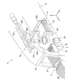
- FIG. 1 is a perspective view illustrating an overall configuration of a component mounter in which a power supply device according to a first embodiment of the present invention is incorporated.
- It is a block diagram which shows the structure of the electric power feeder of 1st Embodiment.
- It is a circuit diagram which shows a half-bridge circuit.
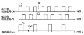
- It is a wave form diagram which shows the high voltage
- It is a circuit diagram which shows the basic circuit of a regulator part.
- FIG. 1 is a perspective view showing the overall configuration of a component mounter 9 in which the power supply apparatus 1 according to the first embodiment of the present invention is incorporated.
- the component mounter 9 is configured by assembling a substrate carrier device 92, a plurality of feeder devices 2, a pallet member 3, a component transfer device 94, a component camera 95, and a control device 96 (shown in FIG. 2) on a machine base 91. Has been.
- the substrate transfer device 92, the feeder device 2, the component transfer device 94, and the component camera 95 are controlled by the control device 96, and each performs a predetermined operation.
- Substrate transport device 92 carries substrate K into the mounting position, positions it, and carries it out.
- the substrate transfer device 92 includes first and second guide rails 921, 922, a pair of conveyor belts, a clamp device, and the like.
- the first and second guide rails 921 and 922 are assembled to the machine base 91 so as to extend in the transport direction (X-axis direction) across the upper center of the machine base 91 and to be parallel to each other.
- a pair of endless annular conveyor belts (not shown) are arranged in parallel inside the first and second guide rails 921 and 922 facing each other.
- the pair of conveyor belts rotate in a state where both edges of the substrate K are placed on the conveyor conveyance surface, and carry the substrate K to and from the mounting position set in the center of the machine base 91.
- a clamp device (not shown) is provided below the conveyor belt at the mounting position. The clamp device pushes up the substrate K, clamps it in a horizontal posture, and positions it at the mounting position. As a result, the component transfer device 94 can perform the mounting operation at the mounting position.
- the plurality of feeder devices 2 sequentially supply electronic components.
- the feeder device 2 has a flat shape that extends in the vertical direction (Z-axis direction) and the front-back direction (Y-axis direction) and has a thin width direction (X-axis direction).
- the plurality of feeder devices 2 are mounted side by side in the width direction (X-axis direction) of the upper surface of the pallet member 3.
- Each feeder device 2 includes a main body portion 22, a supply reel 23 provided at the rear portion of the main body portion 22, and a component extraction portion 24 provided at the front end of the main body portion 22.
- An elongated tape (not shown) in which a large number of electronic components are stored at a predetermined pitch is wound and held on the supply reel 23.
- the tape is fed out by a predetermined pitch by a mechanism portion (not shown), and the electronic components are released from the stored state and sequentially supplied to the component take-out portion 24.
- the feeder device 2 has a motor 46 (shown in FIG. 2) in the mechanism portion, and further has a component supply control unit 44 (shown in FIG. 2) that controls the operation of the motor 46.
- the pallet member 3 is a member for mounting a plurality of feeder devices 2, and is detachably held on the upper surface of the machine base 91.
- the pallet member 3 is a member belonging to the main body of the component mounting machine 9 and includes a bottom plate portion 31 and a front plate portion 32.
- the bottom plate portion 31 has a rectangular plate shape, and its width dimension (X-axis direction dimension) is smaller than the width dimension of the machine base 91.
- a combination of the positioning portion and the engaging portion a combination of a groove-shaped slot carved in the Y-axis direction and a convex portion inserted into the slot can be exemplified.
- the front plate portion 32 is erected from the front edge of the bottom plate portion 31.
- the feeder device 2 is mounted in contact with the bottom plate portion 31 and the front plate portion 32 of the pallet member 3.
- the component transfer device 94 sucks and collects components from each component take-out unit 24 of the plurality of feeder devices 2 and transports and mounts them to the positioned substrate K.
- the component transfer device 94 is an XY robot type device that can move horizontally in the X-axis direction and the Y-axis direction.
- the component transfer device 94 includes a pair of Y-axis rails 941 and 942, a Y-axis slider 943, a head holding unit 944, a suction nozzle 945, and the like.
- the pair of Y-axis rails 941 and 942 extend in the longitudinal direction (Y-axis direction) of the machine base 91 and are disposed above the substrate transfer device 92 and the feeder device 2.
- a Y-axis slider 943 is mounted on the Y-axis rails 941 and 942 so as to be movable in the Y-axis direction.
- a head holding portion 944 is mounted on the Y-axis slider 943 so as to be movable in the X-axis direction.
- the head holding unit 944 is driven in two horizontal directions (X-axis and Y-axis directions) by two servo motors.
- the head holding unit 944 holds the suction nozzle 945 on the lower side thereof in a replaceable manner.
- the suction nozzle 945 has a suction opening at the lower end, and sucks electronic components into the suction opening using negative pressure.
- the component camera 95 is provided upward on the upper surface of the machine base 91 between the substrate transfer device 92 and the feeder device 2.
- the component camera 95 captures and detects the state of the sucked electronic component while the suction nozzle 945 moves from the feeder device 2 onto the substrate K.
- the control device 96 finely adjusts the component mounting operation as necessary, and discards the component if mounting is difficult. To do.
- the control device 96 is provided on the machine base 91.
- the control device 96 holds a mounting sequence specifying the order of mounting electronic components on the substrate K and the feeder device 2 that supplies the electronic components.
- the control device 96 controls the component mounting operation according to the mounting sequence based on the imaging data of the component camera 5 and the detection data of a sensor (not shown).
- the control device 96 sequentially collects and updates operation data such as the number of boards K that have been produced, the mounting time required for mounting electronic components, and the number of occurrences of component suction errors.
- the power feeding device 1 of the first embodiment is a device that feeds power from the pallet member 3 to a plurality of feeder devices 2 by a non-contact power feeding method.
- the pallet member 3 corresponds to the power supply side device of the present invention, the main body of the substrate working machine, and the main body of the component mounting machine 9.
- the feeder device 2 corresponds to a power receiving side device, a mounting device, and a component supply device of the present invention.
- FIG. 2 is a block diagram illustrating a configuration of the power feeding device 1 according to the first embodiment. In FIG. 2, a range corresponding to one feeder device 2 is shown by a single line connection diagram. The thick arrows shown in FIG. 2 indicate the flow of power, and the thin arrows indicate the flow of information and control.
- the feeder device 2 includes a power receiving coil 41, a rectifying unit 42, a regulator unit 43, and a power receiving side link unit 45 as components of the power feeding device 1.
- the feeder device 2 includes a component supply control unit 44 and a motor 46 as electric loads to be fed.
- the pallet member 3 includes a DC power source 51, a half bridge circuit 52, a power supply coil 53, a power supply side control unit 54, a half bridge control unit 55, and a power supply side linkage unit 56 as components of the power supply device 1.
- the power supply coil 53 and the power reception coil 41 are an electromagnetic coupling type non-contact power supply element and a non-contact power reception element.
- the power feeding coil 53 and the power receiving coil 41 can be replaced with other types of elements, for example, a pair of electrostatic coupling type electrodes.
- the DC power source 51 on the pallet member 3 side is connected to both ends of the half bridge circuit 52 and supplies a predetermined DC voltage Vd.
- Examples of the DC power supply 51 include a rectification type power supply device that rectifies and outputs an AC of commercial frequency.
- FIG. 3 is a circuit diagram showing the half-bridge circuit 52.
- the half-bridge circuit 52 is configured by connecting a high-voltage side switching element 52H and a low-voltage side switching element 52L in series with an output terminal 529 interposed therebetween. More specifically, in the high voltage side switching element 52H, the positive side terminal 521 is connected to the positive side terminal 511 of the DC power source 51, the negative side terminal 522 is connected to the output terminal 529, and the control terminal 523 is connected to the half bridge control unit 55. It is connected.
- the positive terminal 524 is connected to the output terminal 529
- the negative terminal 525 is connected to the negative terminal 512 of the DC power supply 51
- the control terminal 526 is connected to the half bridge controller 55.
- the output terminal 529 is connected to one end 531 of the power supply coil 53
- the negative terminal 525 of the low voltage side switching element 52 ⁇ / b> L is connected to the other end 532 of the power supply coil 53.
- the DC power supply 51 and the half bridge circuit 52 correspond to the voltage adjustment power supply unit of the present invention.
- the feeding coil 53 is formed by winding a conductor a predetermined number of times around a C-type core, an E-type core, or the like.
- the power supply coil 53 can be configured by appropriately applying a known technique.
- a resonance circuit may be configured by connecting a resonance capacitor in series or in parallel to the power supply coil 53.
- the above-described core and resonance capacitor are not essential components.
- the power supply side control unit 54 exchanges information with the component supply control unit 44 via the power supply side linkage unit 56 and the power reception side linkage unit 45. In addition, the power supply side control unit 54 exchanges information with the control device 96 corresponding to the host control unit of the present invention. The power supply side control unit 54 exchanges information regarding the operation of the motor 46 to grasp a mechanism operation time zone in which the motor 46 of each feeder device 2 may operate. The power supply side control unit 54 sets a time zone other than the mechanism operation time zone as the control operation time zone.
- the power supply side control unit 54 sends to the half bridge control unit 55 a set voltage command CV that is different between the mechanism operation time zone and the control operation time zone.
- the set voltage command CV is, for example, a binary command that is “High” in the mechanism operation time zone and “Low” in the control operation time zone.
- the power supply side control unit 54 can be configured to include a CPU that operates by software.
- the time zone in which the motor 46 of each feeder device 2 operates is mainly controlled by the control device 96.
- the control device 96 can grasp the feeder device 2 from which the electronic component has been extracted from the component extraction unit 24 by the suction nozzle 945 in accordance with the progress of executing the mounting sequence described above. Therefore, the control device 96 sends the command information for the component supply operation to the feeder device 2 in which the electronic components in the component take-out unit 24 have been exhausted.
- This command information is relayed by the power supply side control unit 54, and is transmitted to the component supply control unit 44 via the power supply side linkage unit 56 and the power reception side linkage unit 45.
- the component supply control unit 44 operates the motor 46 in accordance with the command information and executes a component supply operation.
- the power supply side control unit 54 can grasp the mechanism operation time zone of the feeder device 2 based on the command information that has been relayed.
- the method for controlling the time zone in which the motor 46 operates is not limited to the above, and there are various other methods.
- a sensor for detecting the presence / absence of an electronic component in the component take-out unit 24 is provided in the feeder device 2 so that the component supply control unit 44 autonomously operates the motor 46 when the electronic component is collected and disappears. be able to.
- the power supply side control unit 54 can grasp the mechanism operation time zone of the feeder device 2 by receiving information for operating the motor 46 from the component supply control unit 44.
- the power supply side control unit 54 can grasp the mechanism operation time zone of the feeder device 2 by sharing the time schedule.
- information exchange between the power supply side control unit 54 and the component supply control unit 44 and information exchange between the power supply side control unit 54 and the control device 96 are not essential.
- the half bridge control unit 55 functions as a part of the power supply side control unit 54.
- the half bridge control unit 55 variably controls the generation frequency of the high-voltage side control signal CH and the low-voltage side control signal CL according to the set voltage command CV.
- the half bridge control unit 55 outputs the high voltage side control signal CH to the control terminal 523 of the high voltage side switching element 52H of the half bridge circuit 52 (shown in FIG. 2).
- the half bridge control unit 55 outputs the low voltage side control signal CL to the control terminal 526 of the low voltage side switching element 52L of the half bridge circuit 52 (shown in FIG. 2).
- FIG. 4 is a waveform diagram showing the high-pressure side control signal CH and the low-pressure side control signal CL output by the half-bridge control unit 55 during the mechanism operation time period.
- FIG. 5 is a waveform diagram showing the high-voltage side control signal CH and the low-voltage side control signal CL output by the half-bridge control unit 55 during the control operation time period. 4 and 5, the horizontal axis is a common time axis t. 4 and 5, the upper stage shows the high-voltage side control signal CH, the middle stage shows the low-voltage side control signal CL, and the lower stage shows the AC voltage Va output from the half-bridge circuit 52 and applied to the power feeding coil 53, respectively. .
- the half-bridge control unit 55 generates the high-voltage side control signal CH and the low-voltage side control signal CL alternately and exclusively.
- the signal duration T1 during which the high-voltage side control signal CH is generated, the positive-side terminal 521 and the negative-side terminal 522 of the high-voltage side switching element 52H are in a conductive state.
- the low voltage side control signal CL is not generated during the signal duration T1, and the positive side terminal 524 and the negative side terminal 525 of the low voltage side switching element 52L are cut off.
- the power supply coil 53 is in a state where a DC voltage Vd is applied between the terminals 531 and 532.
- the high-voltage side control signal CH is not generated during the signal duration T2 during which the low-voltage side control signal CL is generated.
- the high-voltage side switching element 52H is cut off and the low-voltage side switching element 52L is turned on.
- the feeding coil 53 is disconnected from the DC power supply 51 and is in a no-voltage state in which the terminals 531 and 532 are short-circuited. Therefore, in the power supply coil 53, the state in which the direct current voltage Vd is applied and the state in which there is no voltage are alternately generated. In other words, the alternating current voltage Va is applied.
- the half-bridge control unit 55 receives “High” as the set voltage command CV during the mechanism operation time zone, and generates the highest frequency of the high-voltage side control signal CH and the low-voltage side control signal CL as shown in FIG. High control. As a result, the average value VaM of the AC voltage Va of the power feeding coil 53 in the mechanism operation time period becomes slightly less than half the DC voltage Vd. Further, the half-bridge control unit 55 receives “Low” as the set voltage command CV during the control operation time period and, as shown in FIG. 5, determines the frequency of occurrence of the high-voltage side and low-voltage side control signals CH and CL as the mechanism operation. Control lower than in the time zone. In the example of FIG.
- the waveforms of the high-pressure side and low-pressure side control signals CH and CL are obtained by thinning out every other waveform of FIG. 4.
- the AC voltage Va of the power feeding coil 53 in the control operation time zone is halved in frequency, and the average value VaC is reduced to about half of the average value VaM in the mechanism operation time zone.
- the power receiving coil 41 on the feeder device 2 side is disposed so as to face the power feeding coil 53. That is, the power receiving coil 41 is disposed on the front surface or the bottom surface of the feeder device 2 in accordance with the power feeding coil 53 disposed on the front plate portion 32 or the bottom plate portion 31 of the pallet member 3. Similarly to the power supply coil 53, the power reception coil 41 is formed by winding a conductor around a core. However, the number of turns of the power receiving coil 41 may be different from the number of turns of the power feeding coil 53.
- the power feeding coil 53 and the power receiving coil 41 are arranged to face each other. Then, the cores of both 41 and 53 are joined to form a good magnetic circuit. As a result, the power receiving coil 41 can receive the high frequency power from the power feeding coil 53 in a non-contact manner. Both ends of the power receiving coil 41 are connected to input terminals 421 and 422 of the rectifying unit 42.
- the rectifying unit 42 rectifies the high-frequency power received by the power receiving coil 41 into a direct current and outputs it to the regulator unit 43 and the motor 46.
- the rectifier 42 can be, for example, a full-wave rectifier circuit in which four diodes are bridge-connected, and a smoothing circuit may be used in combination.
- the DC voltage output from the output terminals 423 and 424 of the rectifying unit 42 is defined as the received voltage Vr.
- the power receiving voltage Vr corresponds to the effective voltage value of the high frequency power received by the power receiving coil 41.
- the output terminals 423 and 424 of the rectifying unit 42 and the motor 46 may be directly connected, or an open / close switch may be inserted to be cut off. On the other hand, the output terminals 423 and 424 and the regulator unit 43 are directly connected.
- the regulator unit 43 converts the received voltage Vr into a control voltage VC and outputs it.
- FIG. 6 is a circuit diagram showing a basic circuit of the regulator unit 43. As illustrated, the regulator unit 43 is configured by a step-down switching regulator circuit. First, a connection method related to input / output of the regulator unit 43 will be described.
- the positive side input terminal 431 of the regulator unit 43 is connected to the positive side output terminal 423 of the rectifying unit 42, and the negative side input terminal 432 is connected to the negative side output terminal 424 of the rectifying unit 42.
- the positive side output terminal 433 of the regulator unit 43 is connected to the positive side terminal 441 of the component supply control unit 44, and the negative side output terminal 434 is connected to the negative side terminal 442 of the component supply control unit 44.
- the positive input terminal 431 of the regulator unit 43 is connected to one terminal 436 of the switching element 435.
- a diode 438 is connected between the other terminal 437 of the switching element 435 and the negative input terminal 432.
- the diode 438 allows a current flowing from the negative side input terminal 432 to the other terminal 437 of the switching element 435 and blocks a current in the reverse direction.
- a coil 439 is connected between the other terminal 437 of the switching element 435 and the positive output terminal 433.
- the coil 439 has a function of smoothing the pulsating flow output from the switching element 435.
- the negative input terminal 432 and the negative output terminal 434 are directly connected internally.
- the power supply side control unit 54 relays the command information of the component supply operation, and therefore can grasp the mechanism operation time zone and the control operation time zone of each feeder device 2. Then, during the mechanism operation time period, the power supply side control unit 54 sends “High” as the set voltage command CV to the half bridge control unit 55.
- the half-bridge control unit 55 outputs the high-voltage side control signal CH and the low-voltage side control signal CL with the highest occurrence frequency shown in FIG. 4 to the half-bridge circuit 52.
- the received voltage Vr substantially matches the drive voltage VM, and the motor 46 can be operated.
- the regulator unit 43 outputs the control voltage VC by voltage conversion even when the power reception voltage Vr is high, so that the component supply control unit 44 operates.
- the power supply side control unit 54 sends “Low” as the set voltage command CV to the half bridge control unit 55.
- the half-bridge control unit 55 outputs the high-voltage side control signal CH and the low-voltage side control signal CL, which are shown in FIG.
- the received voltage Vr decreases to about half of the drive voltage VM, and the motor 46 does not operate.
- the regulator unit 43 converts the relatively low power reception voltage Vr and outputs the control voltage VC, the component supply control unit 44 operates. At this time, since the command information for the component supply operation is not sent to the feeder device 2, no trouble occurs even if the motor 46 cannot be operated.
- FIG. 7 is a diagram schematically showing changes in the element voltage Vsw and the element current Isw when the switching element 435 of the regulator unit 43 changes from the cut-off state to the conductive state.
- the period from the start time t1 to the end time t2 is the switching time ⁇ t.
- the element voltage Vsw is a voltage generated between one terminal 436 and the other terminal 437 of the switching element 435 (shown in FIG. 6), and the element current Isw is a current flowing from the one terminal 436 toward the other terminal 437. (See FIG. 6).
- the element voltage Vsw and the element current Isw change linearly during the switching operation, they are simply modeled. Further, the element voltage Vsw indicated by the solid line in FIG. 7 is in the case of the mechanism operation time zone, and the element voltage Vsw2 indicated by the broken line is in the case of the control operation time zone.
- the switching element 435 Before the start time t1, the switching element 435 can be regarded as a complete cutoff state. Therefore, the element voltage Vsw matches the received voltage Vr, and the element current Isw is zero. It can be considered that the resistance value of the switching element 435 changes during the switching time ⁇ t. That is, when the resistance value decreases from infinity to a finite value at the start time t1, the element current Isw starts to flow and the element voltage Vsw starts to decrease. Furthermore, the resistance value decreases with the passage of time, the device current Isw increases, and the device voltage Vsw decreases. At the end time t2, the switching element 435 can be regarded as a complete conduction state.
- Equation 1 the loss Wt is proportional to the received voltage Vr output from the rectifier 42. Therefore, when the power receiving voltage Vr is lowered as shown by the broken line in FIG. 7, the loss Wt of the regulator unit 43 is reduced in proportion.
- the device voltage Vsw and the device current Isw change nonlinearly, but it is certain that the loss Wt is reduced qualitatively. Therefore, the loss Wt of the regulator unit 43 in the control operation time period is smaller than that in the conventional technique that does not decrease the power reception voltage Vr.
- the generation frequency of the high-pressure side control signal CH and the low-pressure side control signal CL in the control operation time period is not limited to the control that is halved, and the generation frequency is controlled to (1/3), (1/4), or the like. May be.
- the purpose of controlling the occurrence frequency to be low is to variably adjust the average value VaC of the AC voltage Va of the power supply coil 53 to optimize the power reception voltage Vr. Therefore, based on this point of view, an appropriate value of the occurrence frequency can be set so that the received voltage Vr decreases until it substantially matches the control voltage VC. At this time, since the regulator unit 43 does not have a boosting function, it is not preferable to reduce the received voltage Vr to less than the control voltage VC.
- the loss Wt increases when the received voltage Vr becomes smaller than the control voltage VC43. That is, it is best to match the power reception voltage Vr in the control operation time zone with the control voltage VC, and the loss Wt can be minimized.
- the power supply apparatus 1 controls the operation of the motor 46 by being supplied with a drive voltage VM and a motor 46 (mechanism) that operates intermittently and a control voltage VC lower than the drive voltage VM.
- a power feeding device 1 that feeds power from a pallet member 3 (power feeding side device) toward a feeder device 2 (power receiving side device) having a component supply control unit 44 (power receiving side control unit), and is provided in the feeder device 2.
- a regulator unit 43 that converts the received voltage Vr received by feeding into the control voltage VC, a DC power source 51 and a half-bridge circuit 52 (voltage adjustment feeding unit) that are provided on the pallet member 3 and feed the received voltage Vr in an adjustable manner.
- a power supply side control unit 54 and a half bridge control unit 55 which are provided on the pallet member 3 and control the half bridge circuit 52 to control the received voltage Vr.
- the power supply side control unit 54 grasps the mechanism operation time zone in which the motor 46 may operate, and enables the motor 46 to operate by substantially matching the received voltage Vr with the drive voltage VM in the mechanism operation time zone. In the control operation time zone other than the mechanism operation time zone, the power reception voltage Vr is lowered below the drive voltage VM.
- the power supply side control unit 54 enables the operation of the motor 46 by substantially matching the received voltage Vr with the drive voltage VM during the mechanism operation time zone, and during the control operation time zone other than the mechanism operation time zone.
- the power receiving voltage Vr is lowered below the driving voltage VM.
- the feeder apparatus 2 can receive a high power reception voltage Vr that substantially matches the drive voltage VM during the mechanism operation time period in which the motor 46 may operate, and the motor 46 and the component supply control unit 44 can reliably To work.
- the feeder device 2 receives the low power reception voltage Vr, and the component supply control unit 44 operates reliably.
- the conversion efficiency of the regulator unit 43 is improved, and the power loss and temperature rise of the feeder device 2 are effectively reduced. . Further, the effective reduction of the temperature rise simplifies the cooling structure such as the radiation fins, and the feeder device 2 is reduced in size and weight.
- the power supply apparatus 1 of the first embodiment includes a power supply side link unit 56 and a power reception side link unit 45 (control link) that exchange information regarding the operation of the motor 46 between the component supply control unit 44 and the power supply side control unit 54.
- the power supply side control unit 54 grasps the mechanism operation time zone by exchanging information with the component supply control unit 44 via the power supply side linkage unit 56 and the power reception side linkage unit 45.
- the power supply side control unit 54 can accurately grasp the mechanism operation time zone by exchanging information with the component supply control unit 44 that is a party that controls the motor 46. Therefore, at the moment when the motor 46 operates, the feeder device 2 can always receive the high power receiving voltage Vr, and the operation reliability is extremely high.
- the power supply side control unit 54 substantially matches the power reception voltage Vr with the control voltage VC during the control operation time period.
- the loss Wt of the regulator unit 43 in the control operation time zone can be minimized, and the effect of reducing the power loss and temperature rise of the feeder device 2 becomes remarkable.
- the power feeding device 1 of the first embodiment includes a power feeding coil 53 (non-contact power feeding element) connected to the half-bridge circuit 52 and a power receiving coil connected to the regulator unit 43 via the rectifying unit 42. 41 (non-contact power receiving element), and when the power feeding coil 53 and the power receiving coil 41 are arranged to face each other, non-contact power feeding using high-frequency alternating current is performed.
- a power feeding coil 53 non-contact power feeding element
- 41 non-contact power receiving element
- the feeder device 2 fed by the non-contact power feeding device 1 has a remarkable effect of reducing power loss and temperature rise.
- the voltage adjustment power supply unit includes a half bridge circuit 52 in which a high-voltage side switching element 52H and a low-voltage side switching element 52L are connected in series with the output terminal 529 interposed therebetween.
- the DC power supply 51 is connected to both ends of the half bridge circuit 52, the output terminal 529 is connected to one end 531 of the power supply coil 53, and the power supply side control unit 54 includes a half bridge control unit 55.
- the half-bridge control unit 55 generates a high-voltage side control signal CH for conducting the high-voltage side switching element 52H and a low-voltage side control signal CL for conducting the low-voltage side switching element 52L exclusively and alternately.
- the generation frequency of the control signal CH and the low-pressure side control signal CL is variably controlled.
- the average value VaC of the AC voltage Va of the power feeding coil 53 can be variably adjusted using the half bridge circuit 52, and the power receiving voltage Vr received by the feeder device 2 can be variably adjusted. Since the half-bridge circuit 52 and the half-bridge control unit 55 have a simple circuit configuration and are inexpensive, they can contribute to cost reduction of the pallet member 3.
- the half-bridge control unit 55 controls the occurrence frequency to be high during the mechanism operation time period while keeping the signal durations T1 and T2 constant, and the occurrence frequency during the control operation time period. Control low.
- the average value VaC of the AC voltage Va of the power feeding coil 53 can be variably adjusted by the control for reducing the generation frequency of the high-voltage side control signal CH and the low-voltage side control signal CL, and finally the feeder device 2
- the received power receiving voltage Vr can be variably adjusted.
- the control for reducing the frequency of occurrence can simplify the configuration of the control circuit as compared with, for example, a method of variably controlling the signal durations T1 and T2 by pulse width modulation.
- the received voltage Vr is substantially matched with the control voltage VC, and the loss Wt of the regulator unit 43 Can be minimized. Therefore, the pallet member 3 can greatly contribute to the cost reduction and has excellent cost performance.
- the power supply side device is a main body of a substrate working machine that performs a predetermined operation on the substrate K
- the power receiving side device is a mounting device mounted on the substrate working machine.
- the main body of the substrate working machine is the pallet member 3 belonging to the main body of the component mounting machine 9 for mounting electronic components on the board K
- the mounting device is detachably mounted on the component mounting machine 9 to be electronic components.
- the mechanism unit includes a motor 46
- the power reception side control unit is a component supply control unit 44 that controls the operation of the motor 46.
- the power supply device 1 of the first embodiment is incorporated in the substrate work machine, particularly the component mounter 9, the effect of reducing the power loss and temperature rise of the feeder device 2 becomes remarkable.
- the control device 96 (upper control unit) provided in the main body of the component mounter specifies the order in which the electronic components are mounted and the feeder device 2 that supplies the electronic components.
- Each command information for operating each motor 46 of the plurality of feeder apparatuses 2 is sent to each component supply control unit 44 via the power supply side control unit 54 according to the progress status of executing the sequence, and the power supply side control unit 54 is sent. Grasps the mechanism operating time zone of each motor 46 of the plurality of feeder apparatuses 2 based on each command information.
- the electric power feeding side control part 54 can grasp
- FIG. 8 is a block diagram illustrating a configuration of a power feeding apparatus 1A according to the second embodiment.
- a range corresponding to one feeder apparatus 2A is shown by a single-line connection diagram.
- the thick arrows shown in FIG. 8 indicate the flow of power, and the thin arrows indicate the flow of information and control.
- the feeder device 2A includes a regulator unit 43 and a power receiving terminal 47 as components of the power feeding device 1A, and further includes a motor 46 and a component supply control unit 44A.
- the pallet member 3A includes a drive voltage power supply unit 61, a control voltage power supply unit 62, a power supply side control unit 54A, a power supply changeover switch 63, and a power supply terminal receiving unit 57 as components of the power supply apparatus 1A.
- the driving voltage power supply unit 61 on the pallet member 3 ⁇ / b> A side is a direct current power supply, and supplies a direct current voltage that substantially matches the driving voltage VM to the first input terminal 631 of the power supply changeover switch 63.
- the control voltage power supply unit 62 is a DC power supply, and supplies a DC voltage that substantially matches the control voltage VC to the second input terminal 632 of the power supply changeover switch 63.
- the drive voltage power supply unit 61 and the control voltage power supply unit 62 constitute a voltage adjustment power supply unit of the present invention.
- the power supply changeover switch 63 functions as a part of the power supply side control unit 54A.
- the power supply changeover switch 63 selectively switches one of the first input terminal 631 and the second input terminal 632 to connect to the output terminal 633.
- the output terminal 633 is connected to the power supply terminal receiver 57.
- the switching operation of the power supply changeover switch 63 is controlled by a control signal CS from the power supply side control unit 54A.
- the power feeding terminal receiving portion 57 and the linking terminal receiving portion 58 are combined into one connector receiving portion and disposed on the front plate portion 32 of the pallet member 3A.
- the power supply side control unit 54A exchanges information with the component supply control unit 44A on the feeder device 2A side via the linkage terminal receiving portion 58 and the linkage terminal 48, and also exchanges information with the control device 96 on the main body side. Similarly to the first embodiment, the power supply side control unit 54A grasps the mechanism operation time zone of the feeder device 2A by relaying the command information of the component supply operation from the control device 96 to the component supply control unit 44A. . In addition, the power supply side control unit 54A sets a time zone other than the mechanism operation time zone as the control operation time zone.
- the power supply side control unit 54A sends a control signal CS to the power supply changeover switch 63 according to the distinction between the mechanism operation time zone and the control operation time zone. That is, the power supply side control unit 54A connects the first input terminal 631 to the output terminal 633 during the mechanism operation time period and connects the second input terminal 632 to the output terminal 633 during the control operation time period.
- the power receiving terminal 47 and the linking terminal 48 on the feeder device 2A side are combined into one multi-terminal connector and arranged on the front surface of the feeder device 2A.
- the multi-terminal connector of the feeder device 2A is fitted into the connector receiving portion of the pallet member 3A.
- the power receiving terminal receiving portion 57 and the power receiving terminal 47 come into contact with each other, and contact power feeding becomes possible.
- the voltage received by the power receiving terminal 47 is the power receiving voltage Vr.
- the link terminal receiving portion 58 and the link terminal 48 come into contact with each other, and information exchange between the power supply side control portion 54A and the component supply control portion 44A becomes possible.
- the power receiving terminal 47 is connected to the regulator unit 43 and the motor 46.
- the power receiving terminal 47 and the motor 46 may be directly connected, or an open / close switch may be inserted to be cut off.
- the power receiving terminal 47 and the regulator unit 43 are directly connected.
- the internal circuit configuration of the regulator unit 43 is the same as that of the first embodiment shown in FIG.
- the power supply side controller 54A grasps the mechanism operation time zone and the control operation time zone of each feeder device 2A, and controls the power supply changeover switch 63.
- the first input terminal 631 of the power supply changeover switch 63 is connected to the output terminal 633, and a DC voltage that substantially matches the drive voltage VM of the drive voltage power supply unit 61 is supplied to the power supply terminal receiver 57. Is output from.
- the feeder device 2A receives the drive voltage VM as the power reception voltage Vr.
- the second input terminal 632 of the power supply changeover switch 63 is connected to the output terminal 633, and a DC voltage that substantially matches the control voltage VC of the control voltage power supply unit 62 is supplied from the power supply terminal receiver 57. Is output.
- the feeder apparatus 2A receives the control voltage VC as the power reception voltage Vr.
- the loss Wt of the regulator unit 43 in the control operation time zone is reduced as compared with the conventional technique in which the power reception voltage Vr is not lowered, as described in the first embodiment. That is, also in the second embodiment of the contact power feeding method, similarly to the first embodiment of the non-contact power feeding method, the power loss and temperature rise of the feeder device 2A are effectively reduced.
- FIG. 9 is a block diagram illustrating a configuration of a power feeding device 1B according to the third embodiment.
- FIG. 9 only three of the n feeder devices 2 mounted on the pallet member 3B are indicated by a one-dot chain line, and the corresponding range is indicated by a single-line connection diagram.
- the thick arrows shown in FIG. 9 indicate the flow of power, and the thin arrows indicate the flow of information and control.
- the feeder device 2 includes a power receiving coil 41, a rectifying unit 42, a regulator unit 43, and a power receiving side link unit 45 as components of the power feeding device 1B. Since the configuration of the feeder device 2 is the same as that of the first embodiment, description thereof is omitted.
- the pallet member 3B includes, as components of the power supply apparatus 1B, a drive voltage power supply unit 71, a control voltage power supply unit 72, a power supply side control unit 54B, n power supply changeover switches 73, n power supply coils 53, and n. Each of the power supply side linkage portions 56 is provided.
- the driving voltage power supply unit 71 on the pallet member 3B side includes the DC power source 51, the half bridge circuit 52, and the half bridge control unit 55 described in the first embodiment.
- the half-bridge control unit 55 does not receive the set voltage command CV, and always controls the highest occurrence frequency of the high-voltage side control signal CH and the low-voltage side control signal CL.
- the drive voltage power supply unit 71 always outputs the average value VaM of the AC voltage Va shown in FIG.
- the output destination of the average value VaM of the AC voltage Va extends across the first input terminals 731 of all n power supply changeover switches 73.
- control voltage power supply unit 72 also includes the DC power supply 51, the half bridge circuit 52, and the half bridge control unit 55 described in the first embodiment.
- the half bridge control unit 55 does not receive the set voltage command CV, and always controls the occurrence frequency of the high voltage side control signal CH and the low voltage side control signal CL to be low.
- the control voltage power supply unit 72 always outputs the average value VaC (about half of the average value VaM) of the AC voltage Va shown in FIG.
- the output destination of the average value VaC of the AC voltage Va extends over the second input terminals 732 of all n power supply changeover switches 73.
- the drive voltage power supply unit 71 and the control voltage power supply unit 72 constitute a voltage adjustment power supply unit of the present invention.
- the n power supply selector switches 73 function as part of the power supply side control unit 54B. Each power supply selector switch 73 selectively switches one of the first input terminal 731 and the second input terminal 732 to connect to the output terminal 733. Each output terminal 733 is connected to n power supply coils 53 on a one-to-one basis. The switching operation of the power supply selector switch 73 is individually and independently controlled by a control signal CR from the power supply side control unit 64A.
- the power supply side control unit 54B exchanges information independently with the component supply control unit 44 on the feeder device 2 side via each of the n power supply side linkage units 56.
- the power supply side control unit 54B also exchanges information with the control device 96 on the main body side.
- the power feeding side control unit 54B relays the command information of the component supply operation from the control device 96 to the n component supply control units 44, so that the n feeder devices 2 Understand the mechanism operating time individually.
- the power supply side control unit 54B sets a time zone other than the mechanism operation time zone of each feeder device 2 as a control operation time zone.
- the power supply side control unit 54B individually sends a control signal CR to each power supply changeover switch 73 in accordance with the time zone of each feeder device 2. That is, the power supply side control unit 54B connects the first input terminal 731 of the power supply changeover switch 73 to the output terminal 733 in order to supply power from the drive voltage power supply unit 71 toward the feeder device 2 corresponding to the mechanism operation time zone. Further, the power supply side control unit 54B connects the second input terminal 732 of the power supply changeover switch 73 to the output terminal 733 in order to supply power from the control voltage power supply unit 72 toward the feeder device 2 corresponding to the control operation time zone.
- the feeder device 2 corresponding to the mechanism operation time zone is supplied with power from the drive voltage power supply unit 71, and the received voltage Vr substantially matches the drive voltage VM. Further, the feeder device 2 corresponding to the control operation time zone is supplied with power from the control voltage supply unit 72, and the received voltage Vr is lower than the drive voltage VM. Therefore, the effect of effectively reducing the power loss and temperature rise of each feeder device 2 is the same as in the first and second embodiments.
- the power supply device 1B of the third embodiment includes n (a plurality of) feeder devices 2 having the regulator unit 43, and the voltage adjustment power supply unit is adjusted so that the received voltage Vr substantially matches the drive voltage VM.
- Drive voltage power supply unit 71 and control voltage power supply unit 72 adjusted so that received voltage Vr is lower than drive voltage VM.
- Power supply side control unit 54B is directed toward feeder device 2 corresponding to the mechanism operating time zone. Power is supplied from the drive voltage power supply unit 71, and power is supplied from the control voltage power supply unit 72 toward the feeder device 2 corresponding to the control operation time zone.
- n sets of half-bridge circuits 52 and half-bridge control units 55 required for the n feeder apparatuses 2 in the first embodiment are replaced with one set of drive voltage supply unit 71 and control voltage supply unit. 72. Therefore, the structure on the pallet member 3 side is simplified, which can greatly contribute to the cost reduction of the pallet member 3.
- the average value VaC of the AC voltage Va of the power supply coil 53 can be obtained by shortening the signal duration time T1 of the high-voltage side control signal CH to reduce the duty ratio or by controlling the DC voltage Vd of the DC power supply 51 to be low. Can be reduced. Further, the average value VaC of the AC voltage Va of the power feeding coil 53 may be lowered by a circuit configuration different from that of the half bridge circuit 52 and the half bridge control unit 55. Furthermore, the voltage conversion method of the regulator unit 43 on the feeder device 2 side may be different. Various other applications and modifications are possible for the present invention.
- the power feeding device of the present invention is a type of substrate working machine, an assembling machine that produces other products, and a process. It can be used for a wide range of machines.
Landscapes
- Engineering & Computer Science (AREA)
- Manufacturing & Machinery (AREA)
- Microelectronics & Electronic Packaging (AREA)
- Power Engineering (AREA)
- Computer Networks & Wireless Communication (AREA)
- Operations Research (AREA)
- Supply And Installment Of Electrical Components (AREA)
- Direct Current Feeding And Distribution (AREA)
Abstract
Description

2、2A:フィーダ装置(受電側装置、搭載装置)
3、3A、3B:パレット部材(給電側装置、対基板作業機の本体)
41:受電用コイル(非接触受電用素子) 42:整流部
43:レギュレータ部 435:スイッチング素子
44:部品供給制御部(受電側制御部)
45:受電側連係部(制御連係部) 46:モータ
47:受電用端子 48:連係用端子
51:直流電源 52:ハーフブリッジ回路
52H:高圧側スイッチング素子
52L:低圧側スイッチング素子
53:給電用コイル(非接触給電用素子)
54、54A、54B:給電側制御部
55:ハーフブリッジ制御部 56:給電側連係部(制御連係部)
57:給電用端子受け部 58:連係用端子受け部
61:駆動電圧給電部 62:制御電圧給電部
63:給電切替スイッチ
71:駆動電圧給電部 72:制御電圧給電部
73:給電切替スイッチ
9:部品実装機 91:機台 92:基板搬送装置
94:部品移載装置 95:部品カメラ 96:制御装置
Claims (10)
- 駆動電圧が供給されて間欠的に動作する機構部と、前記駆動電圧よりも低い制御電圧が供給されて前記機構部の動作を制御する受電側制御部とを有する受電側装置に向けて、給電側装置から給電する給電装置であって、
前記受電側装置に設けられ、給電によって受け取る受電電圧を前記制御電圧に変換するレギュレータ部と、
前記給電側装置に設けられ、前記受電電圧を調整可能に給電する電圧調整給電部と、
前記給電側装置に設けられ、前記電圧調整給電部を制御して前記受電電圧を制御する給電側制御部と、を備え、
前記給電側制御部は、前記機構部が動作する可能性のある機構動作時間帯を把握し、前記機構動作時間帯には前記受電電圧を前記駆動電圧に概ね一致させて前記機構部の動作を可能とし、前記機構動作時間帯以外の制御動作時間帯には前記受電電圧を前記駆動電圧よりも低下させる給電装置。 - 前記受電側制御部と前記給電側制御部との間で前記機構部の動作に関する情報を交換する制御連係部をさらに備え、
前記給電側制御部は、前記制御連係部を経由した前記受電側制御部との情報交換により前記機構動作時間帯を把握する請求項1に記載の給電装置。 - 前記給電側制御部は、前記制御動作時間帯には前記受電電圧を前記制御電圧に概ね一致させる請求項1または2に記載の給電装置。
- 前記電圧調整給電部に接続された非接触給電用素子と、前記レギュレータ部に接続された非接触受電用素子とをさらに備え、前記非接触給電用素子と前記非接触受電用素子とが対向配置されたときに高周波交流を用いた非接触給電を行う請求項1~3のいずれか一項に記載の給電装置。
- 前記電圧調整給電部は、出力端子を挟んで高圧側スイッチング素子と低圧側スイッチング素子とが直列接続されたハーフブリッジ回路を含んで構成され、前記ハーフブリッジ回路の両端に直流電源が接続され、前記出力端子が前記非接触給電用素子に接続されており、
前記給電側制御部は、前記高圧側スイッチング素子を導通させる高圧側制御信号、および前記低圧側スイッチング素子を導通させる低圧側制御信号を交互に排他的に発生し、かつ、前記高圧側制御信号および前記低圧側制御信号の発生頻度および信号継続時間の少なくとも一方を可変に制御するハーフブリッジ制御部を含む請求項4に記載の給電装置。 - 前記ハーフブリッジ制御部は、前記信号継続時間を一定として、前記機構動作時間帯には前記発生頻度を高く制御し、前記制御動作時間帯には前記発生頻度を低く制御する請求項5に記載の給電装置。
- 前記レギュレータ部を有する受電側装置が複数台あり、
前記電圧調整給電部は、前記受電電圧が前記駆動電圧に概ね一致するように調整された駆動電圧給電部、および前記受電電圧が前記駆動電圧よりも低下するように調整された制御電圧給電部からなり、
前記給電側制御部は、前記機構動作時間帯にあたる受電側装置に向けて前記駆動電圧給電部から給電させるとともに、前記制御動作時間帯にあたる受電側装置に向けて前記制御電圧給電部から給電させる請求項1~4のいずれか一項に記載の給電装置。 - 前記給電側装置は、基板に所定の作業を行う対基板作業機の本体であり、前記受電側装置は、前記対基板作業機に搭載される搭載装置である請求項1~7のいずれか一項に記載の給電装置。
- 前記対基板作業機の本体は、前記基板に電子部品を装着する部品実装機の本体であり、前記搭載装置は、前記部品実装機に着脱可能に搭載されて前記電子部品を供給する複数台のフィーダ装置であって、前記機構部はモータを含み、前記受電側制御部は前記モータの動作を制御する請求項8に記載の給電装置。
- 前記部品実装機の本体に設けられた上位制御部は、前記電子部品を装着する順序および前記電子部品を供給するフィーダ装置を指定した装着シーケンスの進行状況に応じ、前記給電側制御部を経由して複数台の前記フィーダ装置の各前記モータを動作させる各指令情報を各前記受電側制御部に送出し、
前記給電側制御部は、各前記指令情報に基づいて複数台の前記フィーダ装置の各前記モータの前記機構動作時間帯を把握する請求項9に記載の給電装置。
Priority Applications (3)
| Application Number | Priority Date | Filing Date | Title |
|---|---|---|---|
| PCT/JP2014/069027 WO2016009525A1 (ja) | 2014-07-17 | 2014-07-17 | 給電装置 |
| JP2016534042A JP6353046B2 (ja) | 2014-07-17 | 2014-07-17 | 給電装置 |
| US15/325,731 US10566837B2 (en) | 2014-07-17 | 2014-07-17 | Power supply device |
Applications Claiming Priority (1)
| Application Number | Priority Date | Filing Date | Title |
|---|---|---|---|
| PCT/JP2014/069027 WO2016009525A1 (ja) | 2014-07-17 | 2014-07-17 | 給電装置 |
Publications (1)
| Publication Number | Publication Date |
|---|---|
| WO2016009525A1 true WO2016009525A1 (ja) | 2016-01-21 |
Family
ID=55078043
Family Applications (1)
| Application Number | Title | Priority Date | Filing Date |
|---|---|---|---|
| PCT/JP2014/069027 Ceased WO2016009525A1 (ja) | 2014-07-17 | 2014-07-17 | 給電装置 |
Country Status (3)
| Country | Link |
|---|---|
| US (1) | US10566837B2 (ja) |
| JP (1) | JP6353046B2 (ja) |
| WO (1) | WO2016009525A1 (ja) |
Cited By (1)
| Publication number | Priority date | Publication date | Assignee | Title |
|---|---|---|---|---|
| JP2017221020A (ja) * | 2016-06-07 | 2017-12-14 | 本田技研工業株式会社 | 電力供給システム及び電力供給方法 |
Families Citing this family (1)
| Publication number | Priority date | Publication date | Assignee | Title |
|---|---|---|---|---|
| US9300147B2 (en) | 2011-06-29 | 2016-03-29 | Lg Electronics Inc. | Method for avoiding signal collision in wireless power transfer |
Citations (4)
| Publication number | Priority date | Publication date | Assignee | Title |
|---|---|---|---|---|
| JPH11164559A (ja) * | 1997-11-28 | 1999-06-18 | Toshiba Corp | 交流電圧調整装置 |
| JP2006313806A (ja) * | 2005-05-09 | 2006-11-16 | Matsushita Electric Ind Co Ltd | 電子部品実装用装置および電子部品実装用装置における動力供給制御方法 |
| JP2008098355A (ja) * | 2006-10-11 | 2008-04-24 | Juki Corp | 部品供給装置 |
| JP2010283257A (ja) * | 2009-06-08 | 2010-12-16 | Juki Corp | 電子部品実装装置 |
Family Cites Families (10)
| Publication number | Priority date | Publication date | Assignee | Title |
|---|---|---|---|---|
| JP2008236917A (ja) * | 2007-03-20 | 2008-10-02 | Seiko Epson Corp | 非接触電力伝送装置 |
| JP5659704B2 (ja) * | 2010-08-30 | 2015-01-28 | ソニー株式会社 | 非接触給電システム |
| JP5946287B2 (ja) * | 2012-02-23 | 2016-07-06 | 富士機械製造株式会社 | 部品装着装置 |
| WO2014010057A1 (ja) * | 2012-07-12 | 2014-01-16 | 富士機械製造株式会社 | 非接触給電装置 |
| JP6076355B2 (ja) * | 2012-09-05 | 2017-02-08 | 富士機械製造株式会社 | 非接触給電装置 |
| JP6002513B2 (ja) * | 2012-09-14 | 2016-10-05 | ソニー株式会社 | 非接触給電システム、端末装置および非接触給電方法 |
| EP2903130B1 (en) * | 2012-09-25 | 2017-05-31 | Fuji Machine Mfg. Co., Ltd. | Electrostatically-coupled non-contact power supply device and control method for same |
| JP6049742B2 (ja) * | 2012-09-26 | 2016-12-21 | 富士機械製造株式会社 | 静電結合方式非接触給電装置 |
| WO2014049869A1 (ja) * | 2012-09-28 | 2014-04-03 | 富士機械製造株式会社 | 非接触給電装置 |
| US9400295B2 (en) * | 2013-05-09 | 2016-07-26 | Qualcomm Incorporated | Method and devices for non-intrusive power monitoring |
-
2014
- 2014-07-17 JP JP2016534042A patent/JP6353046B2/ja not_active Expired - Fee Related
- 2014-07-17 WO PCT/JP2014/069027 patent/WO2016009525A1/ja not_active Ceased
- 2014-07-17 US US15/325,731 patent/US10566837B2/en active Active
Patent Citations (4)
| Publication number | Priority date | Publication date | Assignee | Title |
|---|---|---|---|---|
| JPH11164559A (ja) * | 1997-11-28 | 1999-06-18 | Toshiba Corp | 交流電圧調整装置 |
| JP2006313806A (ja) * | 2005-05-09 | 2006-11-16 | Matsushita Electric Ind Co Ltd | 電子部品実装用装置および電子部品実装用装置における動力供給制御方法 |
| JP2008098355A (ja) * | 2006-10-11 | 2008-04-24 | Juki Corp | 部品供給装置 |
| JP2010283257A (ja) * | 2009-06-08 | 2010-12-16 | Juki Corp | 電子部品実装装置 |
Cited By (1)
| Publication number | Priority date | Publication date | Assignee | Title |
|---|---|---|---|---|
| JP2017221020A (ja) * | 2016-06-07 | 2017-12-14 | 本田技研工業株式会社 | 電力供給システム及び電力供給方法 |
Also Published As
| Publication number | Publication date |
|---|---|
| JP6353046B2 (ja) | 2018-07-04 |
| JPWO2016009525A1 (ja) | 2017-06-01 |
| US20170163090A1 (en) | 2017-06-08 |
| US10566837B2 (en) | 2020-02-18 |
Similar Documents
| Publication | Publication Date | Title |
|---|---|---|
| JP5824161B2 (ja) | 駆動装置 | |
| JP6104254B2 (ja) | 非接触給電装置 | |
| JP6049742B2 (ja) | 静電結合方式非接触給電装置 | |
| JP6095661B2 (ja) | 非接触給電装置 | |
| CN107996015B (zh) | 非接触供电装置 | |
| JP6076355B2 (ja) | 非接触給電装置 | |
| JP6353046B2 (ja) | 給電装置 | |
| CN108292861A (zh) | 非接触供电装置 | |
| WO2014049869A1 (ja) | 非接触給電装置 | |
| EP2903130B1 (en) | Electrostatically-coupled non-contact power supply device and control method for same | |
| JP6343003B2 (ja) | 非接触給電装置 | |
| JP2018133930A (ja) | 非接触送電装置、非接触受電装置、および非接触給電システム | |
| JP5946287B2 (ja) | 部品装着装置 | |
| JP6441929B2 (ja) | 非接触給電装置 | |
| WO2019186685A1 (ja) | 非接触受電装置、および非接触給電システム | |
| JP6677523B2 (ja) | 非接触給電装置 | |
| WO2017163388A1 (ja) | 非接触給電装置 | |
| JP5836700B2 (ja) | 基板用作業装置 |
Legal Events
| Date | Code | Title | Description |
|---|---|---|---|
| 121 | Ep: the epo has been informed by wipo that ep was designated in this application |
Ref document number: 14897881 Country of ref document: EP Kind code of ref document: A1 |
|
| ENP | Entry into the national phase |
Ref document number: 2016534042 Country of ref document: JP Kind code of ref document: A |
|
| WWE | Wipo information: entry into national phase |
Ref document number: 15325731 Country of ref document: US |
|
| NENP | Non-entry into the national phase |
Ref country code: DE |
|
| 122 | Ep: pct application non-entry in european phase |
Ref document number: 14897881 Country of ref document: EP Kind code of ref document: A1 |