WO2016009496A1 - Power transistor module - Google Patents
Power transistor module Download PDFInfo
- Publication number
- WO2016009496A1 WO2016009496A1 PCT/JP2014/068804 JP2014068804W WO2016009496A1 WO 2016009496 A1 WO2016009496 A1 WO 2016009496A1 JP 2014068804 W JP2014068804 W JP 2014068804W WO 2016009496 A1 WO2016009496 A1 WO 2016009496A1
- Authority
- WO
- WIPO (PCT)
- Prior art keywords
- conductive pattern
- pattern
- power transistor
- transistor module
- feeding point
- Prior art date
Links
Images


Classifications
-
- H—ELECTRICITY
- H01—ELECTRIC ELEMENTS
- H01L—SEMICONDUCTOR DEVICES NOT COVERED BY CLASS H10
- H01L25/00—Assemblies consisting of a plurality of individual semiconductor or other solid state devices ; Multistep manufacturing processes thereof
- H01L25/18—Assemblies consisting of a plurality of individual semiconductor or other solid state devices ; Multistep manufacturing processes thereof the devices being of types provided for in two or more different subgroups of the same main group of groups H01L27/00 - H01L33/00, or in a single subclass of H10K, H10N
-
- H—ELECTRICITY
- H01—ELECTRIC ELEMENTS
- H01L—SEMICONDUCTOR DEVICES NOT COVERED BY CLASS H10
- H01L23/00—Details of semiconductor or other solid state devices
- H01L23/48—Arrangements for conducting electric current to or from the solid state body in operation, e.g. leads, terminal arrangements ; Selection of materials therefor
-
- H—ELECTRICITY
- H01—ELECTRIC ELEMENTS
- H01L—SEMICONDUCTOR DEVICES NOT COVERED BY CLASS H10
- H01L24/00—Arrangements for connecting or disconnecting semiconductor or solid-state bodies; Methods or apparatus related thereto
- H01L24/01—Means for bonding being attached to, or being formed on, the surface to be connected, e.g. chip-to-package, die-attach, "first-level" interconnects; Manufacturing methods related thereto
- H01L24/42—Wire connectors; Manufacturing methods related thereto
- H01L24/47—Structure, shape, material or disposition of the wire connectors after the connecting process
- H01L24/49—Structure, shape, material or disposition of the wire connectors after the connecting process of a plurality of wire connectors
-
- H—ELECTRICITY
- H01—ELECTRIC ELEMENTS
- H01L—SEMICONDUCTOR DEVICES NOT COVERED BY CLASS H10
- H01L25/00—Assemblies consisting of a plurality of individual semiconductor or other solid state devices ; Multistep manufacturing processes thereof
- H01L25/03—Assemblies consisting of a plurality of individual semiconductor or other solid state devices ; Multistep manufacturing processes thereof all the devices being of a type provided for in the same subgroup of groups H01L27/00 - H01L33/00, or in a single subclass of H10K, H10N, e.g. assemblies of rectifier diodes
- H01L25/04—Assemblies consisting of a plurality of individual semiconductor or other solid state devices ; Multistep manufacturing processes thereof all the devices being of a type provided for in the same subgroup of groups H01L27/00 - H01L33/00, or in a single subclass of H10K, H10N, e.g. assemblies of rectifier diodes the devices not having separate containers
- H01L25/07—Assemblies consisting of a plurality of individual semiconductor or other solid state devices ; Multistep manufacturing processes thereof all the devices being of a type provided for in the same subgroup of groups H01L27/00 - H01L33/00, or in a single subclass of H10K, H10N, e.g. assemblies of rectifier diodes the devices not having separate containers the devices being of a type provided for in group H01L29/00
- H01L25/072—Assemblies consisting of a plurality of individual semiconductor or other solid state devices ; Multistep manufacturing processes thereof all the devices being of a type provided for in the same subgroup of groups H01L27/00 - H01L33/00, or in a single subclass of H10K, H10N, e.g. assemblies of rectifier diodes the devices not having separate containers the devices being of a type provided for in group H01L29/00 the devices being arranged next to each other
-
- H—ELECTRICITY
- H01—ELECTRIC ELEMENTS
- H01L—SEMICONDUCTOR DEVICES NOT COVERED BY CLASS H10
- H01L2224/00—Indexing scheme for arrangements for connecting or disconnecting semiconductor or solid-state bodies and methods related thereto as covered by H01L24/00
- H01L2224/01—Means for bonding being attached to, or being formed on, the surface to be connected, e.g. chip-to-package, die-attach, "first-level" interconnects; Manufacturing methods related thereto
- H01L2224/02—Bonding areas; Manufacturing methods related thereto
- H01L2224/04—Structure, shape, material or disposition of the bonding areas prior to the connecting process
- H01L2224/06—Structure, shape, material or disposition of the bonding areas prior to the connecting process of a plurality of bonding areas
- H01L2224/0601—Structure
- H01L2224/0603—Bonding areas having different sizes, e.g. different heights or widths
-
- H—ELECTRICITY
- H01—ELECTRIC ELEMENTS
- H01L—SEMICONDUCTOR DEVICES NOT COVERED BY CLASS H10
- H01L2224/00—Indexing scheme for arrangements for connecting or disconnecting semiconductor or solid-state bodies and methods related thereto as covered by H01L24/00
- H01L2224/01—Means for bonding being attached to, or being formed on, the surface to be connected, e.g. chip-to-package, die-attach, "first-level" interconnects; Manufacturing methods related thereto
- H01L2224/42—Wire connectors; Manufacturing methods related thereto
- H01L2224/47—Structure, shape, material or disposition of the wire connectors after the connecting process
- H01L2224/48—Structure, shape, material or disposition of the wire connectors after the connecting process of an individual wire connector
- H01L2224/4805—Shape
- H01L2224/4809—Loop shape
- H01L2224/48091—Arched
-
- H—ELECTRICITY
- H01—ELECTRIC ELEMENTS
- H01L—SEMICONDUCTOR DEVICES NOT COVERED BY CLASS H10
- H01L2224/00—Indexing scheme for arrangements for connecting or disconnecting semiconductor or solid-state bodies and methods related thereto as covered by H01L24/00
- H01L2224/01—Means for bonding being attached to, or being formed on, the surface to be connected, e.g. chip-to-package, die-attach, "first-level" interconnects; Manufacturing methods related thereto
- H01L2224/42—Wire connectors; Manufacturing methods related thereto
- H01L2224/47—Structure, shape, material or disposition of the wire connectors after the connecting process
- H01L2224/48—Structure, shape, material or disposition of the wire connectors after the connecting process of an individual wire connector
- H01L2224/481—Disposition
- H01L2224/48135—Connecting between different semiconductor or solid-state bodies, i.e. chip-to-chip
- H01L2224/48137—Connecting between different semiconductor or solid-state bodies, i.e. chip-to-chip the bodies being arranged next to each other, e.g. on a common substrate
-
- H—ELECTRICITY
- H01—ELECTRIC ELEMENTS
- H01L—SEMICONDUCTOR DEVICES NOT COVERED BY CLASS H10
- H01L2224/00—Indexing scheme for arrangements for connecting or disconnecting semiconductor or solid-state bodies and methods related thereto as covered by H01L24/00
- H01L2224/01—Means for bonding being attached to, or being formed on, the surface to be connected, e.g. chip-to-package, die-attach, "first-level" interconnects; Manufacturing methods related thereto
- H01L2224/42—Wire connectors; Manufacturing methods related thereto
- H01L2224/47—Structure, shape, material or disposition of the wire connectors after the connecting process
- H01L2224/49—Structure, shape, material or disposition of the wire connectors after the connecting process of a plurality of wire connectors
- H01L2224/491—Disposition
- H01L2224/4911—Disposition the connectors being bonded to at least one common bonding area, e.g. daisy chain
- H01L2224/49113—Disposition the connectors being bonded to at least one common bonding area, e.g. daisy chain the connectors connecting different bonding areas on the semiconductor or solid-state body to a common bonding area outside the body, e.g. converging wires
-
- H—ELECTRICITY
- H01—ELECTRIC ELEMENTS
- H01L—SEMICONDUCTOR DEVICES NOT COVERED BY CLASS H10
- H01L24/00—Arrangements for connecting or disconnecting semiconductor or solid-state bodies; Methods or apparatus related thereto
- H01L24/01—Means for bonding being attached to, or being formed on, the surface to be connected, e.g. chip-to-package, die-attach, "first-level" interconnects; Manufacturing methods related thereto
- H01L24/42—Wire connectors; Manufacturing methods related thereto
- H01L24/47—Structure, shape, material or disposition of the wire connectors after the connecting process
- H01L24/48—Structure, shape, material or disposition of the wire connectors after the connecting process of an individual wire connector
-
- H—ELECTRICITY
- H01—ELECTRIC ELEMENTS
- H01L—SEMICONDUCTOR DEVICES NOT COVERED BY CLASS H10
- H01L2924/00—Indexing scheme for arrangements or methods for connecting or disconnecting semiconductor or solid-state bodies as covered by H01L24/00
- H01L2924/0001—Technical content checked by a classifier
- H01L2924/00014—Technical content checked by a classifier the subject-matter covered by the group, the symbol of which is combined with the symbol of this group, being disclosed without further technical details
-
- H—ELECTRICITY
- H01—ELECTRIC ELEMENTS
- H01L—SEMICONDUCTOR DEVICES NOT COVERED BY CLASS H10
- H01L2924/00—Indexing scheme for arrangements or methods for connecting or disconnecting semiconductor or solid-state bodies as covered by H01L24/00
- H01L2924/10—Details of semiconductor or other solid state devices to be connected
- H01L2924/11—Device type
- H01L2924/13—Discrete devices, e.g. 3 terminal devices
- H01L2924/1304—Transistor
- H01L2924/1305—Bipolar Junction Transistor [BJT]
- H01L2924/13055—Insulated gate bipolar transistor [IGBT]
-
- H—ELECTRICITY
- H01—ELECTRIC ELEMENTS
- H01L—SEMICONDUCTOR DEVICES NOT COVERED BY CLASS H10
- H01L2924/00—Indexing scheme for arrangements or methods for connecting or disconnecting semiconductor or solid-state bodies as covered by H01L24/00
- H01L2924/10—Details of semiconductor or other solid state devices to be connected
- H01L2924/11—Device type
- H01L2924/13—Discrete devices, e.g. 3 terminal devices
- H01L2924/1304—Transistor
- H01L2924/1306—Field-effect transistor [FET]
- H01L2924/13091—Metal-Oxide-Semiconductor Field-Effect Transistor [MOSFET]
Definitions
- the present invention relates to a module configured by mounting a power transistor such as IGBT or MOSFET on a circuit board, and more particularly to its internal wiring structure.
- MOSFETs Metal-Oxide-Semiconductor-Field-Effect-Transistors
- IGBTs Insulated-Gate-Bipolar-Transistors
- a metal wiring pattern of a predetermined shape is disposed on one surface of a heat sink of metal or the like via an insulating substrate, and a semiconductor element is soldered on the metal wiring pattern by a method such as soldering. It is mounted and electrically connected to an external connection terminal (external lead-out terminal) by a bonding wire or the like.
- a circuit board a combination of an insulating substrate and a metal wiring pattern is referred to as a circuit board.
- a plurality of semiconductor elements may be connected in parallel on a metal wiring pattern of a predetermined shape inside the module.
- Patent Literature 1 discloses a technique for reducing variation in impedance from a semiconductor element arranged in parallel to an external lead-out terminal.
- Patent Document 1 by providing a slit in the internal connection portion, the impedance from each semiconductor element to the external lead-out terminal is equalized, and the internal connection portion also serves as a heat dissipation structure, so that the semiconductor element and the internal connection portion are arranged.
- a semiconductor device that can reduce thermal stress of a bonding wire to be connected is disclosed.
- the semiconductor device disclosed in Patent Document 1 takes out a case, a plurality of semiconductor circuit boards each having a semiconductor element mounted on an insulating substrate provided in the case and provided with a metal wiring pattern, and a main current is taken out of the case.
- An external lead-out terminal, and an internal connection portion in which a part of the external lead-out terminal extends into the case, is disposed along the plurality of semiconductor substrates, and is electrically joined to the main electrode of the semiconductor element;
- the internal connection part has a heat dissipation means for maintaining heat dissipation and a slit structure for equalizing the current path length from the semiconductor element.
- Patent Document 2 discloses a technique for forming an inductance forming region by inserting a slit for subdividing the width of the current path into the emitter pattern portion on the circuit board.
- the semiconductor elements arranged in parallel on the circuit board have non-uniform impedance to the external lead-out terminals connected to the circuit board, and therefore flow through each semiconductor element. There is a problem that the amount of current is different.
- the slit structure of the semiconductor device of Patent Document 1 is provided not in the semiconductor circuit board but in the internal connection part that connects the circuit boards, the impedance of the external lead-out terminals between the circuit boards arranged in parallel is reduced. Although uniforming is effective, the impedance uniforming effect between parallel chips mounted on a circuit board is considered to be thin.
- the internal connection portion is considered to have a large adverse effect of the interference effect due to the current of the other internal connection portions due to the laminated structure of the plurality of internal connection portions disclosed in FIG.
- the uniform effect is not perfect, and it is considered that variations in impedance remain between individual semiconductor elements arranged in parallel and circuit boards arranged in an array.
- Patent Document 2 has a slit structure on a circuit board constituting a power transistor module, and this makes the inductance values of upper and lower arm transistors constituting a half bridge uniform. The purpose is different from the equalization of impedance between parallel chips mounted on a circuit board.
- an object of the present invention is to provide a highly reliable power transistor module configured by arranging a plurality of semiconductor elements on a circuit board in parallel, with high precision and uniform impedance from each semiconductor element to an external lead-out terminal. It is to provide a power transistor module.
- the present invention provides a power transistor module including at least one circuit board in which a plurality of semiconductor elements are arranged on a main surface of an insulating substrate, wherein the circuit board is formed on the insulating substrate.
- the first conductive pattern includes, at one end thereof, a first feeding point that supplies a potential to the first conductive pattern, at least one diode element on the first conductive pattern,
- a plurality of switching elements are provided on the first conductive pattern opposite to the first feeding point across the diode element, and the second conductive pattern is provided in the vicinity of the first feeding point.
- the second conductive pattern is provided with a slit pattern that defines a connection region of the plurality of bonding wires with the second conductive pattern on the second conductive pattern. It is characterized by.
- the present invention is also a power transistor module including at least one circuit board in which a plurality of semiconductor elements are arranged on a main surface of an insulating substrate, wherein the circuit board is formed on the insulating substrate.
- a conductive pattern and a second conductive pattern formed in a region different from the first conductive pattern on the insulating substrate and electrically insulated from the first conductive pattern.
- the conductive pattern includes a first feeding point that supplies a potential to the first conductive pattern at one end thereof, and the end of the first feeding part opposite to the end provided with the first feeding part.
- a plurality of switching elements arranged along a direction toward an end of the first conductive pattern, wherein the second conductive pattern is provided in the vicinity of the first feeding point; and Different from the conductive pattern A second feeding point for supplying the second conductive pattern to the second conductive pattern, and the plurality of switching elements are electrically connected to the second conductive pattern by a plurality of bonding wires.
- the conductive pattern is provided with a slit pattern that defines a connection region of the plurality of bonding wires with the second conductive pattern on the second conductive pattern.
- the impedance from each semiconductor element to the external lead-out terminal is made uniform with high accuracy, and a highly reliable power transistor.
- a module can be realized.
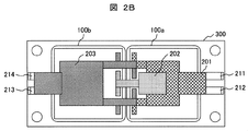
- FIG. 2A and FIG. 2B show the configuration of the power transistor module in this example.
- 2A and 2B show a cross-sectional view and a plan view of the power transistor module, respectively.
- the power transistor module 500 includes a case 400, a metal base 300, external lead-out terminals 201 to 203, control signal terminals 211 to 214, a circuit board 100, and a solder bonding layer 7.
- the case 400 determines the outer shape of the module, and is made of an insulating resin. In the following description, the description of the case 400 is omitted unless particularly necessary.
- the metal base 300 together with the case 400, determines the external shape of the module, and is generated by one or more circuit boards 100 that are made of a metal material and bonded to the heat sink (not shown) by the solder bonding layer 7. It functions as a path to dissipate the generated heat.
- External lead-out terminals 201 to 203 are terminals for connecting a metal (wiring) pattern on the circuit board 100 and a main circuit outside the module, and serve as an input / output path for the energization current of the module.
- the control signal terminals 211 to 214 are terminals for electrically connecting a metal (wiring) pattern on the circuit board 100 and a control signal generation circuit outside the module through bonding wires 61 to 64, and are used for switching elements in the module. This is the control signal path.
- the circuit board 100 includes metal (wiring) patterns 1 and 2, switching element control signal patterns 3 and 4, an insulating substrate 5, and a metal (wiring) pattern 6.
- the number of circuit boards 100 used in the power transistor module is as follows. The function is determined according to the function determined by the rated current capacity and the metal (wiring) pattern.
- the solder bonding layer 7 mechanically and electrically connects the circuit board 100 and the metal base 300.
- the power transistor module in the present embodiment is configured by using two circuit boards, a circuit board 100a and a circuit board 100b, and the external lead-out terminal 201 is connected to the circuit board 100a.
- the external lead-out terminal 202 is connected to a metal pattern at a low potential on the circuit board 100b, and the external lead-out terminal 203 is connected to a metal pattern at a low potential on the circuit board 100a. It has a function of connecting a metal pattern to be a potential.
- the positions where the high-potential and low-potential external lead-out terminals are connected are arranged close to each other as long as there is no problem in mounting technology and insulation design. This is to minimize the loop area of the path through which the current flows from the high potential metal pattern to the low potential metal pattern, and to suppress the inductance generated in the current path.
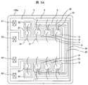
- FIG. 3A shows an example of mounting a metal (wiring) pattern and a semiconductor element on a circuit board 100a in a conventional power transistor module.
- the circuit board 100a connects the high-potential metal pattern 1, the low-potential metal pattern 2, the control signal patterns 3 and 4 of the switching element, the diode elements 21 to 24 formed of a semiconductor, the switching elements 11 to 16, and the semiconductor element It is constituted by bonding wires 31 to 33 and 41 to be performed.
- the metal pattern 1 is electrically connected to the cathode terminals of the diode elements 21 to 24 formed of a semiconductor, and is electrically connected to the collector terminals or drain terminals of the switching elements 11 to 16 formed of a semiconductor.
- feeding positions 51 and 52 for connection to the external lead-out terminal 201 are arranged.
- Anode terminals of the diode elements 21 to 24 are electrically connected to the metal pattern 2 via bonding wires 41, and collector terminals or drain terminals of the switching elements 11 to 16 are electrically connected to each other via bonding wires 31.
- feeding positions 53 and 54 for connection with the external lead-out terminal 203 are arranged.
- the control signal pattern 3 of the switching element is electrically connected to the gate terminal of the switching element via the bonding wire 32, and is connected to a control signal generating circuit (not shown) outside the module via the bonding wire 61. ing.
- the control signal pattern 4 of the switching element is electrically connected to the source terminal of the switching element via the bonding wire 33, and is connected to a control signal generating circuit (not shown) outside the module via the bonding wire 62. ing.
- the feeding positions 51 and 52 for connection with the external lead-out terminal 201 and the feeding positions 53 and 54 for connection with the external lead-out terminal 203 are close to each other in order to reduce the inductance of the current path flowing through the circuit board 100a. Deploy.
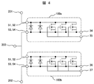
- FIG. 4 shows an equivalent circuit when the circuit board shown in FIG. 3A is mounted on the power transistor module shown in FIG. 2A.
- the switching elements mounted on the circuit boards 100a and 100b are assumed to be FET type elements. It goes without saying that the effect of the present invention does not change even if the switching element is an IGBT type element.
- the equivalent circuit of the power transistor module shown in FIG. 4 is a half-bridge circuit in which the upper arm is constituted by the circuit board 100a and the lower arm is constituted by the circuit board 100b.
- the external lead-out terminal 201 is a high potential side main terminal
- the external lead-out terminal 202 is a low potential side main terminal
- the external lead-out terminal 203 is an intermediate potential main terminal.
- the equivalent circuit of this circuit board shows an example of a parallel circuit of two diode elements and three FET elements.
- the problem to be solved by the present invention is the non-uniformity of the current between the three FET elements as described above, in particular, the non-uniformity of the transient current that occurs when the power transistor module is switched.
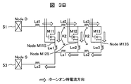
- FIG. 3B current non-uniformity of a power transistor module using a conventional circuit board, that is, a circuit board in which a metal pattern on the circuit board is not provided with a slit will be described.
- FIG. 3B is an equivalent circuit in which the upper half of the element arrangement of FIG. 3A is simplified. Since an equivalent circuit is made by paying attention to the current path when the power transistor module on which the circuit board is mounted is turned on, the diode element is omitted.
- NodeD indicates a feeding position 51 for connection to the external lead-out terminal 201 of the metal pattern 1
- inductors Ld1 to Ld3 indicate inductances of current paths on the metal pattern 1 from NodeD to the drains of the FET elements M11 to M13.
- inductors Lw1 to Lw3 are arranged as equivalent circuit representations of bonding wires, and Ls1 to Ls3 are arranged as inductances of current paths on the metal pattern 2.
- NodeS indicates a power feeding position 53 for connection to the external lead-out terminal 203 on the metal pattern 2. In the figure, the direction of current flow is indicated by arrows.
- magnetic coupling occurs between the inductor Ld2 on the metal pattern 1 and the inductor Ls1 on the metal pattern 2 through the gap between the patterns, and has a mutual inductance M2 determined by the coupling coefficient K2.
- the power feeding position 51 for connection with the external lead-out terminal 201 and the power feeding position 53 for connection with the external lead-out terminal 203 are arranged in the vicinity, and the current directions of the metal pattern 1 and the metal pattern 2 are in opposite directions. Therefore, the mutual inductance has an effect of canceling (reducing) the mutual self-inductance. The same applies to the inductor Ld3 and the inductor Ls2.
- the configuration and effect of the power transistor module in the present embodiment will be described with reference to FIGS. 5A and 5B.
- the circuit board of FIG. 5A is provided with two L-shaped slit patterns 62 in the metal pattern 2 in addition to the configuration described in the description of FIG. 3A above.
- the diode element is arranged in the vicinity
- the FET element is arranged in the distance
- the slit pattern 62 is arranged in the longitudinal direction of the slit pattern 62. It arrange
- the slit pattern 62 is formed in an L shape in the metal pattern 2, and a connection region between the plurality of bonding wires and the metal pattern 2 is for connecting the L shape slit pattern 62 and the external lead-out terminal 203.
- a connection region between the plurality of bonding wires and the metal pattern 2 is for connecting the L shape slit pattern 62 and the external lead-out terminal 203.
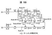
- FIG. 5B is an equivalent circuit obtained by simplifying the upper half of the element arrangement of FIG. 5A. Since an equivalent circuit is made by paying attention to the current path when the power transistor module on which the circuit board is mounted is turned on, the diode element is omitted.
- NodeD indicates a feeding position 51 for connection to the external lead-out terminal 201 of the metal pattern 1, and inductors Ld1 to Ld3 indicate inductances of current paths on the metal pattern 1 from NodeD to the drains of the FET elements M11 to M13. Show.
- Inductors Lw1 to Lw3 are arranged as equivalent circuit representations of bonding wires at the sources of the FET elements M11 to M13, and Ls1 to Ls7 are arranged as inductances of current paths on the metal pattern 2.
- the slit pattern 62 extends the current path of the metal pattern 2 and generates magnetic coupling by mutual inductance.
- NodeS indicates a power feeding position 53 for connection to the external lead-out terminal 203 on the metal pattern 2. In the figure, the direction of current flow is indicated by arrows.
- M2 increases the coupled self-inductance because the current flows in the same direction.
- the relationship between the inductor Ld3 and the inductor Ls2 is the same.
- the current direction is opposite, so the mutual inductance M1 has an effect of reducing the self-inductance.
- the relationship between the inductors Ls2 and Ls5 is the same.
- the average absolute value of the inductance is 11 nH in the case of the conventional circuit board pattern shown by the equivalent circuit in FIG. 3B and 22 nH in the case of the present embodiment. From the above description, it can be seen that the inductance variation of the current path of the FET element in which the circuit board pattern of the present embodiment in which the slit pattern 62 is introduced is arranged in parallel is reduced, and the uniformity of the inductance value is improved.
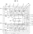
- FIG. 1A A second embodiment of the present invention and its effects will be described with reference to FIGS. 1A and 1B.
- the circuit board pattern in FIG. 1A is obtained by replacing the slit pattern 62 in FIG. 5A described in the description of the first embodiment with one U-shaped slit pattern 63 arranged inside the metal pattern 2 as shown in the figure. It is.
- the slit pattern 63 is formed in a U-shape in the metal pattern 2, and a connection region between the plurality of bonding wires and the metal pattern 2 is a connection between the U-shaped slit pattern 63 and the external lead-out terminal 203. Is provided in a region surrounded by a side opposite to one side of the metal pattern 2 in the vicinity of the power feeding position 53 for.
- the power feed position 51 for connection with the external lead-out terminal 201 arranged in the vicinity and the power feed position 53 for connection with the external lead-out terminal 203 or the external lead-out terminal 201 are connected.
- a diode element is disposed in the vicinity and an FET element is disposed far from a power feeding position 54 for connection between the power feeding position 52 for connection and the external lead-out terminal 203, and the slit pattern 63 is disposed of a plurality of FET elements.
- the slit pattern 63 is arranged so that the direction in which they are aligned is the longitudinal direction of the slit pattern 63. Further, since the slit pattern 63 is arranged inside the metal pattern 2, the following two advantages are generated.
- the first advantage is that the area of the metal pattern 2 can be reduced because it can also serve as an arrangement point of the bonding wire from the source electrode of the FET element arranged symmetrically on the circuit board 100a.
- the area where the bonding wires are arranged above and below the metal pattern is set.
- the area can also be used, and the bonding wire area can be reduced to about 1 ⁇ 2. it can.
- the second advantage is that the direction of the current flowing through the circuit board 100a is reversed between all adjacent patterns. Thereby, the mutual inductance due to the magnetic coupling between the adjacent patterns has an effect of reducing the self-inductance, and an increase in the absolute value of the inductance which is a reaction due to the introduction of the slit can be suppressed. This effect will be described in detail with reference to FIG. 1B.
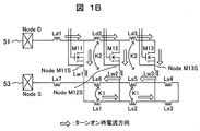
- FIG. 1B is an equivalent circuit obtained by simplifying the upper half of the element arrangement of FIG. 1A. Since an equivalent circuit is made by paying attention to a current path when the power transistor module on which the circuit board 100a is mounted is turned on, a diode element is omitted.
- NodeD indicates a feeding position 51 for connection to the external lead-out terminal 201 of the metal pattern 1
- inductors Ld1 to Ld3 indicate inductances of current paths on the metal pattern 1 from NodeD to the drains of the FET elements M11 to M13. Show.
- inductors Lw1 to Lw3 are arranged as equivalent circuit representations of bonding wires, and Ls1 to Ls7 are arranged as inductances of current paths on the metal pattern 2.
- the slit pattern 63 extends the current path of the metal pattern 2 and generates magnetic coupling due to mutual inductance.
- NodeS indicates a power feeding position 53 for connection to the external lead-out terminal 203 on the metal pattern 2. In the figure, the direction of current flow is indicated by arrows.
- magnetic coupling occurs between the inductor Ld2 on the metal pattern 1 and the inductor Ls6 on the metal pattern 2 through the gap between the patterns, and has a mutual inductance M2 determined by the coupling coefficient K2. .
- M2 reduces the coupled self-inductance because the direction of current flow is opposite.
- the relationship between the inductor Ld3 and the inductor Ls5 is the same.
- the average absolute value of the inductance is 11 nH in the case of the conventional circuit board pattern shown by the equivalent circuit in FIG. 3B, and is about 15 nH in this embodiment, which is higher than that in the first embodiment. It is clear that the inductance variation between the paths can be reduced while keeping the inductance low. From the above description, it can be seen that both the inductance of the current path and the inductance variation of the FET element in which the circuit board pattern of the present embodiment in which the slit pattern 63 is introduced are arranged in parallel are reduced.
- the circuit board pattern shown in FIG. 6 is the same as the slit pattern described in the description of the second embodiment except that the power feeding position 51 for connection to the external lead-out terminal 201 and the power feed position for connection to the external lead-out terminal 203 are illustrated. 53 or the feeding position 52 for connection to the external lead-out terminal 201 and the feeding position 54 for connection to the external lead-out terminal 203, the slit width is monotonously increased widely as the distance is increased. .
- the absolute value of the inductance can be adjusted by the substantially U-shaped slit pattern 64 having the non-uniform slit width. That is, by using the circuit board 100a of the present embodiment, it is possible to obtain an advantage that the absolute value and variation value of the inductance can be adjusted by changing the design of only the slit pattern width of the circuit board.
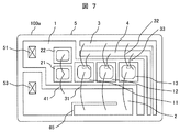
- the circuit board pattern in FIG. 7 is a circuit board pattern having the configuration of the upper half of the circuit board pattern in FIG. 1A described in the second embodiment.
- the metal pattern 1 is provided on both sides of the circuit board 100a, that is, the metal pattern 2 of the circuit board 100a in FIGS. 1A, 5A, and 6 and above and below the circuit board 100a.
- a description has been given using a configuration in which a plurality of diode elements and a plurality of switching elements are arranged on 1, as shown in FIG. 7, a plurality of diode elements and switching are provided on one side of the circuit board 100a, that is, the upper half region of FIG.
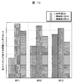
- FIG. 10 shows the effect when the circuit board 100a described in the first and second embodiments is used.
- FIG. 10 shows a relative comparison of path inductances in the switching elements M11 to M13.
- this invention is not limited to the above-mentioned Example, Various modifications are included.
- the above-described embodiments have been described in detail for easy understanding of the present invention, and are not necessarily limited to those having all the configurations described.
- a part of the configuration of one embodiment can be replaced with the configuration of another embodiment, and the configuration of another embodiment can be added to the configuration of one embodiment.
- MOSFET Metal-Oxide-Semiconductor-Field-Effect-Transistor: MOS-type field effect transistor
- J-FET Junction-type electric field
- IGBT Insulated-Gate-Bipolar-Transistor: Insulated Gate Bipolar Transistor
- the effect of the present invention is not changed by using either a PN junction diode or an SB (Shottky-Barrier-junction) diode. Further, even when a diode is formed inside the switching element and a single diode element is not mounted on the circuit board 100a described in each embodiment, a slit is formed in the metal pattern 2 as described in each embodiment. By providing the pattern, it is possible to obtain the same effect as that of each embodiment.
Abstract
Description
経路M11の場合: It becomes. Here, if the values of Ld1 to Ld2 are Ld and the values of Ls1 to L3 are Ls,
For route M11:
経路M11の場合: It becomes. When the values of Ld1 to Ld3 are Ld and the values of Ls1 to L7 are Ls,
For route M11:


経路M11の場合: It becomes. When the values of Ld1 to Ld3 are Ld and the values of Ls1 to L7 are Ls,
For route M11:
3,4…スイッチング素子の制御信号パターン,5…絶縁基板
7…半田接合層
11,12,13,14,15,16…スイッチング素子
21,22,23,24…ダイオード素子
31,32,33,34,35,36,37,41…ボンディングワイヤ
51,52…外部導出端子201との接続のための給電位置
53,54…外部導出端子203との接続のための給電位置
62,63,64,65,66,67…スリットパターン
100,100a,100b…回路基板
201,202,203…外部導出端子
211,212,213,214…制御信号端子
300…金属ベース
400…ケース
500…パワートランジスタモジュール
K1,K2…結合係数
Ld1,Ld2,Ld3,Lw1,Lw2,Lw3,Ls1,Ls2,Ls3,Ls4,Ls5,Ls6,Ls7…インダクタ
M1,M2…相互インダクタンス
M11,M12,M13…FET素子。 DESCRIPTION OF
Claims (11)
- 絶縁基板の主面に複数の半導体素子が配置された回路基板を少なくとも1つ以上含むパワートランジスタモジュールであって、
前記回路基板は、前記絶縁基板上に形成された第1の導電パターンと、
前記絶縁基板上の前記第1の導電パターンとは異なる領域に、前記第1の導電パターンと電気的に絶縁して形成された第2の導電パターンと、を備え、
前記第1の導電パターンは、その一端に前記第1の導電パターンに電位を供給する第1の給電点と、
前記第1の導電パターン上に少なくとも1つ以上のダイオード素子と、
前記ダイオード素子を挟んで前記第1の給電点と反対側の前記第1の導電パターン上に複数のスイッチング素子を有し、
前記第2の導電パターンは、前記第1の給電点の近傍に設けられ、かつ、前記第1の導電パターンとは異なる電位を前記第2の導電パターンに供給する第2の給電点と、を有し、
前記複数のスイッチング素子は、複数のボンディングワイヤにより前記第2の導電パターンと電気的に接続され、
前記第2の導電パターンは、前記第2の導電パターン上における前記複数のボンディングワイヤの前記第2の導電パターンとの接続領域を規定するスリットパターンが設けられていることを特徴とするパワートランジスタモジュール。 A power transistor module including at least one circuit board in which a plurality of semiconductor elements are arranged on a main surface of an insulating substrate,
The circuit board includes a first conductive pattern formed on the insulating substrate;
A second conductive pattern formed in a region different from the first conductive pattern on the insulating substrate and electrically insulated from the first conductive pattern;
The first conductive pattern has a first feeding point that supplies a potential to the first conductive pattern at one end thereof;
At least one diode element on the first conductive pattern;
A plurality of switching elements on the first conductive pattern opposite to the first feeding point across the diode element;
The second conductive pattern is provided in the vicinity of the first power supply point, and a second power supply point that supplies a potential different from that of the first conductive pattern to the second conductive pattern. Have
The plurality of switching elements are electrically connected to the second conductive pattern by a plurality of bonding wires,
The power transistor module, wherein the second conductive pattern is provided with a slit pattern that defines a connection region of the plurality of bonding wires with the second conductive pattern on the second conductive pattern. . - 絶縁基板の主面に複数の半導体素子が配置された回路基板を少なくとも1つ以上含むパワートランジスタモジュールであって、
前記回路基板は、絶縁基板上に形成された第1の導電パターンと、
前記絶縁基板上の前記第1の導電パターンとは異なる領域に、前記第1の導電パターンと電気的に絶縁して形成された第2の導電パターンと、を備え、
前記第1の導電パターンは、その一端に前記第1の導電パターンに電位を供給する第1の給電点と、
前記第1の給電部から前記第1の給電部が設けられた端部の反対側の前記第1の導電パターンの端部に向かう方向に沿って配置された複数のスイッチング素子を有し、
前記第2の導電パターンは、前記第1の給電点の近傍に設けられ、かつ、前記第1の導電パターンとは異なる電位を前記第2の導電パターンに供給する第2の給電点と、を有し、
前記複数のスイッチング素子は、複数のボンディングワイヤにより前記第2の導電パターンと電気的に接続され、
前記第2の導電パターンは、前記第2の導電パターン上における前記複数のボンディングワイヤの前記第2の導電パターンとの接続領域を規定するスリットパターンが設けられていることを特徴とするパワートランジスタモジュール。 A power transistor module including at least one circuit board in which a plurality of semiconductor elements are arranged on a main surface of an insulating substrate,
The circuit board includes a first conductive pattern formed on an insulating substrate;
A second conductive pattern formed in a region different from the first conductive pattern on the insulating substrate and electrically insulated from the first conductive pattern;
The first conductive pattern has a first feeding point that supplies a potential to the first conductive pattern at one end thereof;
A plurality of switching elements arranged along a direction from the first power supply unit toward the end of the first conductive pattern on the side opposite to the end provided with the first power supply unit;
The second conductive pattern is provided in the vicinity of the first power supply point, and a second power supply point that supplies a potential different from that of the first conductive pattern to the second conductive pattern. Have
The plurality of switching elements are electrically connected to the second conductive pattern by a plurality of bonding wires,
The power transistor module, wherein the second conductive pattern is provided with a slit pattern that defines a connection region of the plurality of bonding wires with the second conductive pattern on the second conductive pattern. . - 前記スリットパターンは、前記第2の導電パターン内にコの字型に形成され、前記複数のボンディングワイヤと前記第2の導電パターンとの接続領域は、前記コの字型のスリットパターンと前記第2の給電部近傍の前記第2の導電パターンの一辺とは反対側の辺により囲まれた領域に設けられていることを特徴とする請求項1または2に記載のパワートランジスタモジュール。 The slit pattern is formed in a U-shape in the second conductive pattern, and a connection region between the plurality of bonding wires and the second conductive pattern is formed in the U-shaped slit pattern and the second conductive pattern. 3. The power transistor module according to claim 1, wherein the power transistor module is provided in a region surrounded by a side opposite to one side of the second conductive pattern in the vicinity of the two power supply units.
- 前記スリットパターンは、前記第2の導電パターン内にL字型に形成され、前記複数のボンディングワイヤと前記第2の導電パターンとの接続領域は、前記L字型のスリットパターンと前記第2の給電部近傍の前記第2の導電パターンの一辺とは反対側の辺を含む前記第2の導電パターンの二辺により囲まれた領域に設けられていることを特徴とする請求項1または2に記載のパワートランジスタモジュール。 The slit pattern is formed in an L-shape in the second conductive pattern, and a connection region between the plurality of bonding wires and the second conductive pattern is formed in the L-shaped slit pattern and the second conductive pattern. 3. The method according to claim 1, wherein the second conductive pattern is provided in a region surrounded by two sides of the second conductive pattern including a side opposite to one side of the second conductive pattern in the vicinity of the power feeding unit. The power transistor module described.
- 前記スリットパターンは、前記第2の導電パターン内において、前記第2の給電点から遠ざかるに従い、スリットの幅が単調増加的に広くなっていることを特徴とする請求項1から4のいずれかに記載のパワートランジスタモジュール。 5. The slit pattern according to claim 1, wherein the slit pattern monotonically increases in width as the distance from the second feeding point increases in the second conductive pattern. The power transistor module described.
- 前記複数のスイッチング素子は、前記第2の導電パターンの長手方向に沿って前記第1の導電パターン上に配置され、前記スリットパターンの長手方向は、前記第2の導電パターンの長手方向に沿うように設けられていることを特徴とする請求項1から5のいずれかに記載のパワートランジスタモジュール。 The plurality of switching elements are disposed on the first conductive pattern along a longitudinal direction of the second conductive pattern, and a longitudinal direction of the slit pattern is along a longitudinal direction of the second conductive pattern. The power transistor module according to claim 1, wherein the power transistor module is provided on the power transistor module.
- 前記第1の導電パターンは、前記複数のスイッチング素子のうち少なくとも1つのスイッチング素子のドレイン電極と電気的に接続し、
前記第2の導電パターンは、前記複数のスイッチング素子のうち少なくとも1つのスイッチング素子のソース電極と電気的に接続していることを特徴とする請求項1から6のいずれかに記載のパワートランジスタモジュール。 The first conductive pattern is electrically connected to a drain electrode of at least one of the plurality of switching elements;
The power transistor module according to claim 1, wherein the second conductive pattern is electrically connected to a source electrode of at least one switching element among the plurality of switching elements. . - 前記第1の給電点および前記第2の給電点に各々異なる電位の電力を供給し、前記パワートランジスタモジュールを動作させた際、前記第2の導電パターンに前記第1の導電パターンを流れる電流の方向と反対方向の電流が生じるよう前記第2の導電パターンに前記スリットパターンを設けたことを特徴とする請求項1から7のいずれかに記載のパワートランジスタモジュール。 When electric power having different potentials is supplied to the first feeding point and the second feeding point, respectively, and the power transistor module is operated, the current flowing through the first conductive pattern to the second conductive pattern The power transistor module according to any one of claims 1 to 7, wherein the slit pattern is provided in the second conductive pattern so that a current in a direction opposite to the direction is generated.
- 前記第1の給電点および前記第2の給電点に各々異なる電位の電力を供給し、前記パワートランジスタモジュールを動作させた際、前記第1の導電パターンおよび前記第2の導電パターンの各々に流れる電流の方向が互いに隣接する電流に対し逆方向に流れるよう前記第2の導電パターンに前記スリットパターンを設けたことを特徴とする請求項1から8のいずれかに記載のパワートランジスタモジュール。 When power having different potentials is supplied to the first feeding point and the second feeding point, respectively, and the power transistor module is operated, the first and second conductive patterns flow. The power transistor module according to any one of claims 1 to 8, wherein the slit pattern is provided in the second conductive pattern so that the direction of current flows in a direction opposite to currents adjacent to each other.
- 前記スリットパターンの長手方向の長さは、前記第1の給電点および前記第2の給電点に各々異なる電位の電力を供給し、前記パワートランジスタモジュールを動作させた際、前記複数のスイッチング素子の電流経路に発生するインダクタンスの値の偏差が最小となる長さであることを特徴とする請求項1から9のいずれかに記載のパワートランジスタモジュール。 The length of the slit pattern in the longitudinal direction is such that when the power transistor module is operated by supplying different electric powers to the first feeding point and the second feeding point, the plurality of switching elements The power transistor module according to any one of claims 1 to 9, wherein the power transistor module has a length that minimizes a deviation of an inductance value generated in the current path.
- 前記スリットパターンの長手方向の長さは、前記第1の給電点および前記第2の給電点に各々異なる電位の電力を供給し、前記パワートランジスタモジュールを動作させた際、前記複数のスイッチング素子のソース端子或いはエミッタ端子から前記第2の給電点までの電流経路に発生するインダクタンスの値の偏差が最小となる長さであることを特徴とする請求項1から10のいずれかに記載のパワートランジスタモジュール。 The length of the slit pattern in the longitudinal direction is such that when the power transistor module is operated by supplying different electric powers to the first feeding point and the second feeding point, the plurality of switching elements 11. The power transistor according to claim 1, wherein the power transistor has a length that minimizes a deviation of an inductance value generated in a current path from a source terminal or an emitter terminal to the second feeding point. module.
Priority Applications (3)
| Application Number | Priority Date | Filing Date | Title |
|---|---|---|---|
| PCT/JP2014/068804 WO2016009496A1 (en) | 2014-07-15 | 2014-07-15 | Power transistor module |
| JP2016534021A JP6405383B2 (en) | 2014-07-15 | 2014-07-15 | Power transistor module |
| US15/325,784 US10002858B2 (en) | 2014-07-15 | 2014-07-15 | Power transistor module |
Applications Claiming Priority (1)
| Application Number | Priority Date | Filing Date | Title |
|---|---|---|---|
| PCT/JP2014/068804 WO2016009496A1 (en) | 2014-07-15 | 2014-07-15 | Power transistor module |
Publications (1)
| Publication Number | Publication Date |
|---|---|
| WO2016009496A1 true WO2016009496A1 (en) | 2016-01-21 |
Family
ID=55078017
Family Applications (1)
| Application Number | Title | Priority Date | Filing Date |
|---|---|---|---|
| PCT/JP2014/068804 WO2016009496A1 (en) | 2014-07-15 | 2014-07-15 | Power transistor module |
Country Status (3)
| Country | Link |
|---|---|
| US (1) | US10002858B2 (en) |
| JP (1) | JP6405383B2 (en) |
| WO (1) | WO2016009496A1 (en) |
Cited By (7)
| Publication number | Priority date | Publication date | Assignee | Title |
|---|---|---|---|---|
| WO2017163612A1 (en) * | 2016-03-24 | 2017-09-28 | 株式会社日立製作所 | Power semiconductor module |
| WO2020170553A1 (en) * | 2019-02-18 | 2020-08-27 | 富士電機株式会社 | Semiconductor device |
| JP2021072293A (en) * | 2019-10-29 | 2021-05-06 | 三菱電機株式会社 | Semiconductor power module |
| CN113630113A (en) * | 2020-05-08 | 2021-11-09 | 株式会社东芝 | Semiconductor device with a plurality of semiconductor chips |
| US11521933B2 (en) | 2018-04-18 | 2022-12-06 | Fuji Electric Co., Ltd. | Current flow between a plurality of semiconductor chips |
| DE102023106586A1 (en) | 2022-04-25 | 2023-10-26 | Fuji Electric Co., Ltd. | SEMICONDUCTOR DEVICE |
| JP7428019B2 (en) | 2020-03-06 | 2024-02-06 | 富士電機株式会社 | semiconductor module |
Families Citing this family (4)
| Publication number | Priority date | Publication date | Assignee | Title |
|---|---|---|---|---|
| JP6786416B2 (en) * | 2017-02-20 | 2020-11-18 | 株式会社東芝 | Semiconductor device |
| DE112019000178T5 (en) | 2018-06-01 | 2020-09-03 | Fuji Electric Co., Ltd. | SEMI-CONDUCTOR DEVICE |
| US10763193B2 (en) | 2018-10-30 | 2020-09-01 | Hamilton Sundstrand Corporation | Power control modules |
| JP2021064674A (en) * | 2019-10-11 | 2021-04-22 | 富士電機株式会社 | Semiconductor device |
Citations (4)
| Publication number | Priority date | Publication date | Assignee | Title |
|---|---|---|---|---|
| JPH0729932A (en) * | 1993-07-12 | 1995-01-31 | Origin Electric Co Ltd | Power semiconductor device |
| JP2001094035A (en) * | 1999-09-27 | 2001-04-06 | Toshiba Corp | Semiconductor device |
| JP2002203941A (en) * | 2001-01-04 | 2002-07-19 | Nissan Motor Co Ltd | Semiconductor packaging structure |
| JP2006203974A (en) * | 2005-01-18 | 2006-08-03 | Fuji Electric Fa Components & Systems Co Ltd | Wiring structure of power converter |
Family Cites Families (2)
| Publication number | Priority date | Publication date | Assignee | Title |
|---|---|---|---|---|
| JP2973799B2 (en) | 1993-04-23 | 1999-11-08 | 富士電機株式会社 | Power transistor module |
| JP5136343B2 (en) | 2008-10-02 | 2013-02-06 | 三菱電機株式会社 | Semiconductor device |
-
2014
- 2014-07-15 JP JP2016534021A patent/JP6405383B2/en active Active
- 2014-07-15 WO PCT/JP2014/068804 patent/WO2016009496A1/en active Application Filing
- 2014-07-15 US US15/325,784 patent/US10002858B2/en active Active
Patent Citations (4)
| Publication number | Priority date | Publication date | Assignee | Title |
|---|---|---|---|---|
| JPH0729932A (en) * | 1993-07-12 | 1995-01-31 | Origin Electric Co Ltd | Power semiconductor device |
| JP2001094035A (en) * | 1999-09-27 | 2001-04-06 | Toshiba Corp | Semiconductor device |
| JP2002203941A (en) * | 2001-01-04 | 2002-07-19 | Nissan Motor Co Ltd | Semiconductor packaging structure |
| JP2006203974A (en) * | 2005-01-18 | 2006-08-03 | Fuji Electric Fa Components & Systems Co Ltd | Wiring structure of power converter |
Cited By (15)
| Publication number | Priority date | Publication date | Assignee | Title |
|---|---|---|---|---|
| JPWO2017163612A1 (en) * | 2016-03-24 | 2018-09-27 | 株式会社日立製作所 | Power semiconductor module |
| WO2017163612A1 (en) * | 2016-03-24 | 2017-09-28 | 株式会社日立製作所 | Power semiconductor module |
| US11521933B2 (en) | 2018-04-18 | 2022-12-06 | Fuji Electric Co., Ltd. | Current flow between a plurality of semiconductor chips |
| WO2020170553A1 (en) * | 2019-02-18 | 2020-08-27 | 富士電機株式会社 | Semiconductor device |
| JPWO2020170553A1 (en) * | 2019-02-18 | 2021-10-14 | 富士電機株式会社 | Semiconductor device |
| JP7447979B2 (en) | 2019-02-18 | 2024-03-12 | 富士電機株式会社 | semiconductor equipment |
| JP7201066B2 (en) | 2019-02-18 | 2023-01-10 | 富士電機株式会社 | semiconductor equipment |
| US11456244B2 (en) | 2019-02-18 | 2022-09-27 | Fuji Electric Co., Ltd. | Semiconductor device |
| JP2021072293A (en) * | 2019-10-29 | 2021-05-06 | 三菱電機株式会社 | Semiconductor power module |
| US11728251B2 (en) * | 2019-10-29 | 2023-08-15 | Mitsubishi Electric Corporation | Semiconductor power module with temperature sensors and shaped top plate to equalize current paths |
| JP7428019B2 (en) | 2020-03-06 | 2024-02-06 | 富士電機株式会社 | semiconductor module |
| JP2021177519A (en) * | 2020-05-08 | 2021-11-11 | 株式会社東芝 | Semiconductor device |
| US11605613B2 (en) | 2020-05-08 | 2023-03-14 | Kabushiki Kaisha Toshiba | Semiconductor device |
| CN113630113A (en) * | 2020-05-08 | 2021-11-09 | 株式会社东芝 | Semiconductor device with a plurality of semiconductor chips |
| DE102023106586A1 (en) | 2022-04-25 | 2023-10-26 | Fuji Electric Co., Ltd. | SEMICONDUCTOR DEVICE |
Also Published As
| Publication number | Publication date |
|---|---|
| JPWO2016009496A1 (en) | 2017-04-27 |
| JP6405383B2 (en) | 2018-10-17 |
| US20170170157A1 (en) | 2017-06-15 |
| US10002858B2 (en) | 2018-06-19 |
Similar Documents
| Publication | Publication Date | Title |
|---|---|---|
| JP6405383B2 (en) | Power transistor module | |
| US11600602B2 (en) | Semiconductor power module | |
| JP6400201B2 (en) | Power semiconductor module | |
| WO2010131679A1 (en) | Semiconductor device | |
| JP5893369B2 (en) | Semiconductor device | |
| WO2017163612A1 (en) | Power semiconductor module | |
| WO2017169693A1 (en) | Semiconductor module | |
| EP3522213B1 (en) | Semiconductor device | |
| US10396057B2 (en) | Half-bridge power semiconductor module and method for manufacturing same | |
| US20190318999A1 (en) | Semiconductor device | |
| US20230187431A1 (en) | Semiconductor module | |
| JP2018074088A (en) | Semiconductor device | |
| US9655265B2 (en) | Electronic module | |
| US20200091042A1 (en) | Semiconductor device | |
| US20210366813A1 (en) | Power semiconductor module | |
| US11728251B2 (en) | Semiconductor power module with temperature sensors and shaped top plate to equalize current paths | |
| US10855196B2 (en) | Semiconductor device | |
| JP6394459B2 (en) | Semiconductor device | |
| JP2019080014A (en) | Power semiconductor module | |
| JP2013062551A (en) | Semiconductor device | |
| RU2676190C1 (en) | Power semiconductor module with improved structure of contact connectors for welding | |
| JP6541896B1 (en) | Semiconductor module and power converter | |
| WO2023181498A1 (en) | Semiconductor device and power conversion device | |
| JP2019140364A (en) | Semiconductor device |
Legal Events
| Date | Code | Title | Description |
|---|---|---|---|
| 121 | Ep: the epo has been informed by wipo that ep was designated in this application |
Ref document number: 14897732 Country of ref document: EP Kind code of ref document: A1 |
|
| ENP | Entry into the national phase |
Ref document number: 2016534021 Country of ref document: JP Kind code of ref document: A |
|
| WWE | Wipo information: entry into national phase |
Ref document number: 15325784 Country of ref document: US |
|
| NENP | Non-entry into the national phase |
Ref country code: DE |
|
| 122 | Ep: pct application non-entry in european phase |
Ref document number: 14897732 Country of ref document: EP Kind code of ref document: A1 |