WO2015166605A1 - 成膜方法 - Google Patents
成膜方法 Download PDFInfo
- Publication number
- WO2015166605A1 WO2015166605A1 PCT/JP2014/082388 JP2014082388W WO2015166605A1 WO 2015166605 A1 WO2015166605 A1 WO 2015166605A1 JP 2014082388 W JP2014082388 W JP 2014082388W WO 2015166605 A1 WO2015166605 A1 WO 2015166605A1
- Authority
- WO
- WIPO (PCT)
- Prior art keywords
- target
- substrate
- film forming
- film
- coupled plasma
- Prior art date
- Legal status (The legal status is an assumption and is not a legal conclusion. Google has not performed a legal analysis and makes no representation as to the accuracy of the status listed.)
- Ceased
Links
Images



Classifications
-
- C—CHEMISTRY; METALLURGY
- C23—COATING METALLIC MATERIAL; COATING MATERIAL WITH METALLIC MATERIAL; CHEMICAL SURFACE TREATMENT; DIFFUSION TREATMENT OF METALLIC MATERIAL; COATING BY VACUUM EVAPORATION, BY SPUTTERING, BY ION IMPLANTATION OR BY CHEMICAL VAPOUR DEPOSITION, IN GENERAL; INHIBITING CORROSION OF METALLIC MATERIAL OR INCRUSTATION IN GENERAL
- C23C—COATING METALLIC MATERIAL; COATING MATERIAL WITH METALLIC MATERIAL; SURFACE TREATMENT OF METALLIC MATERIAL BY DIFFUSION INTO THE SURFACE, BY CHEMICAL CONVERSION OR SUBSTITUTION; COATING BY VACUUM EVAPORATION, BY SPUTTERING, BY ION IMPLANTATION OR BY CHEMICAL VAPOUR DEPOSITION, IN GENERAL
- C23C14/00—Coating by vacuum evaporation, by sputtering or by ion implantation of the coating forming material
-
- C—CHEMISTRY; METALLURGY
- C23—COATING METALLIC MATERIAL; COATING MATERIAL WITH METALLIC MATERIAL; CHEMICAL SURFACE TREATMENT; DIFFUSION TREATMENT OF METALLIC MATERIAL; COATING BY VACUUM EVAPORATION, BY SPUTTERING, BY ION IMPLANTATION OR BY CHEMICAL VAPOUR DEPOSITION, IN GENERAL; INHIBITING CORROSION OF METALLIC MATERIAL OR INCRUSTATION IN GENERAL
- C23C—COATING METALLIC MATERIAL; COATING MATERIAL WITH METALLIC MATERIAL; SURFACE TREATMENT OF METALLIC MATERIAL BY DIFFUSION INTO THE SURFACE, BY CHEMICAL CONVERSION OR SUBSTITUTION; COATING BY VACUUM EVAPORATION, BY SPUTTERING, BY ION IMPLANTATION OR BY CHEMICAL VAPOUR DEPOSITION, IN GENERAL
- C23C14/00—Coating by vacuum evaporation, by sputtering or by ion implantation of the coating forming material
- C23C14/02—Pretreatment of the material to be coated
-
- C—CHEMISTRY; METALLURGY
- C23—COATING METALLIC MATERIAL; COATING MATERIAL WITH METALLIC MATERIAL; CHEMICAL SURFACE TREATMENT; DIFFUSION TREATMENT OF METALLIC MATERIAL; COATING BY VACUUM EVAPORATION, BY SPUTTERING, BY ION IMPLANTATION OR BY CHEMICAL VAPOUR DEPOSITION, IN GENERAL; INHIBITING CORROSION OF METALLIC MATERIAL OR INCRUSTATION IN GENERAL
- C23C—COATING METALLIC MATERIAL; COATING MATERIAL WITH METALLIC MATERIAL; SURFACE TREATMENT OF METALLIC MATERIAL BY DIFFUSION INTO THE SURFACE, BY CHEMICAL CONVERSION OR SUBSTITUTION; COATING BY VACUUM EVAPORATION, BY SPUTTERING, BY ION IMPLANTATION OR BY CHEMICAL VAPOUR DEPOSITION, IN GENERAL
- C23C14/00—Coating by vacuum evaporation, by sputtering or by ion implantation of the coating forming material
- C23C14/06—Coating by vacuum evaporation, by sputtering or by ion implantation of the coating forming material characterised by the coating material
- C23C14/08—Oxides
-
- C—CHEMISTRY; METALLURGY
- C23—COATING METALLIC MATERIAL; COATING MATERIAL WITH METALLIC MATERIAL; CHEMICAL SURFACE TREATMENT; DIFFUSION TREATMENT OF METALLIC MATERIAL; COATING BY VACUUM EVAPORATION, BY SPUTTERING, BY ION IMPLANTATION OR BY CHEMICAL VAPOUR DEPOSITION, IN GENERAL; INHIBITING CORROSION OF METALLIC MATERIAL OR INCRUSTATION IN GENERAL
- C23C—COATING METALLIC MATERIAL; COATING MATERIAL WITH METALLIC MATERIAL; SURFACE TREATMENT OF METALLIC MATERIAL BY DIFFUSION INTO THE SURFACE, BY CHEMICAL CONVERSION OR SUBSTITUTION; COATING BY VACUUM EVAPORATION, BY SPUTTERING, BY ION IMPLANTATION OR BY CHEMICAL VAPOUR DEPOSITION, IN GENERAL
- C23C14/00—Coating by vacuum evaporation, by sputtering or by ion implantation of the coating forming material
- C23C14/22—Coating by vacuum evaporation, by sputtering or by ion implantation of the coating forming material characterised by the process of coating
- C23C14/34—Sputtering
Definitions
- the present invention relates to a film forming method.
- a film formation technique for forming a film on a substrate there is a so-called sputtering technique in which a target made of a material to be a film is sputtered and a film is formed on a substrate disposed facing the target. If impurities (for example, water containing hydrogen atoms) are attached to the target surface, the impurities are mixed into the film formed on the substrate, and the substrate on which the film has been formed (hereinafter referred to as a film formation substrate) is included.
- the reliability of the product may be reduced.
- an oxide semiconductor is attracting attention as a thin film in a thin film transistor (TFT) for high-definition displays, and is usually formed by a magnetron sputtering method. This is a factor that reduces reliability.
- Patent Document 1 a film is formed on a substrate while heating a target made of an oxide semiconductor to 100 ° C. or higher.
- an object of the present invention is to provide a film forming method capable of efficiently forming a film on a substrate.
- a film forming method is arranged to face a target in a film forming chamber by sputtering the target with inductively coupled plasma while supplying sputtering power to the target arranged in the film forming chamber.
- a film forming method for forming a film made of a target material on a formed substrate, a substrate disposing step of disposing a substrate facing the target in a film forming chamber in which the target is disposed, and power for sputtering on the target A cleaning process for cleaning the surface of the target by generating inductively coupled plasma between the target and the substrate in a state where the target is not supplied, and subjecting the surface of the target to plasma treatment with the inductively coupled plasma; Target power is generated by inductively coupled plasma by supplying sputtering power to the target.
- a film forming step of forming a film on the substrate is arranged to face a target in a film forming chamber by sputtering the target with inductively coupled plasma while supplying sputtering power to
- the surface of the target is cleaned by generating inductively coupled plasma in the film forming chamber in the cleaning process before the film forming process.
- cleaning means removing impurities on the surface.
- sputtering power is supplied to the target, and the target is sputtered using inductively coupled plasma.
- inductively coupled plasma does not require time, and since the inductively coupled plasma has a high density, the time required for the cleaning process can be shortened. As a result, in the film forming method, a film can be efficiently formed on the substrate.
- the surface of the substrate may be cleaned together with the surface of the target by subjecting the surface of the substrate together with the surface of the target to plasma treatment with inductively coupled plasma.
- impurities attached to the surface of the substrate are also removed, so that a film with reduced contamination can be more reliably formed on the substrate.
- the target material may include an oxide semiconductor.
- An oxide semiconductor has attracted attention as a material used for a thin film transistor, for example.
- the above film formation method is more effective when the target material includes an oxide semiconductor.
- the oxide semiconductor may be an amorphous oxide semiconductor made of indium, gallium, zinc, and oxygen.
- the target includes the amorphous oxide semiconductor
- impurities are likely to be mixed into the target. Therefore, for example, in the case of plasma in which lighting of the plasma for sputtering depends on the state of the target, it is necessary to perform processing for returning the state of the target to the state before maintenance.
- the state of the target does not depend on the lighting of the inductively coupled plasma. Therefore, even if the film formation chamber is maintained, for example, a process for returning the target state to the pre-maintenance state for plasma lighting after the maintenance is unnecessary. Therefore, a film can be efficiently formed on the substrate.
- a film can be efficiently formed on a substrate.
- FIG. 2 is a schematic diagram of a cross-sectional configuration along the line II-II in FIG. 1. In FIG. 1, it is drawing at the time of seeing the target side from the board
- FIG. 5 is a diagram for explaining a cleaning process shown in FIG. 4. 5 is a diagram illustrating a state of a substrate at a stage where a film forming process illustrated in FIG. 4 is completed.
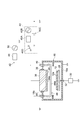
- FIG. 1 is a schematic diagram of a film forming apparatus according to an embodiment.
- the film formation apparatus 10 is an apparatus for forming a film on the substrate 12 by a sputtering method, and is also an apparatus for manufacturing a film-formed substrate (hereinafter also referred to as a film formation substrate).
- the film forming apparatus 10 may constitute a part of a system for manufacturing a thin film transistor (TFT) for a high-definition display, for example.
- TFT thin film transistor
- the saddle substrate 12 may be any one according to the intended use of the film formation substrate.
- the substrate 12 include a deposition substrate on which a film is to be formed when manufacturing a flat panel display such as a liquid crystal display and an organic EL display, a flexible display, and a semiconductor device such as a solar cell.
- the substrate 12 may have a predetermined structure such as a predetermined electrode pattern or a film different from the film formed by the film forming apparatus 10 on the base plate.
- the material of the base plate include glass, semiconductor, and plastic such as polyimide film and polyethylene naphthalate (PEN) film.
- the substrate 12 may be the base plate itself.
- an example of the substrate 12 is an electrode serving as a transistor electrode (for example, a gate electrode) on a glass plate as a base plate.
- a pattern may be formed.
- the surface 12a of the substrate 12 (hereinafter referred to as the substrate surface) is the predetermined formed on the base plate when a predetermined structure such as an electrode pattern is formed on the base plate. And the area of the surface of the base plate (surface on which the predetermined structure is formed) that is not covered with the predetermined structure. When the surface of the base plate is entirely covered with the predetermined structure, the surface of the substrate 12 corresponds to the surface of the predetermined structure.
- the film forming apparatus 10 is divided from the load lock chamber 14 by a gate valve 16 and a film forming chamber 18 as a sputtering treatment chamber for forming a film on the substrate 12 by a sputtering method. Prepare.
- the load lock chamber 14 is a vacuum container (or vacuum chamber) for preventing the inside of the film forming chamber 18 from being opened to the atmosphere when the substrate 12 is disposed in the film forming chamber 18 or when the substrate 12 is taken out from the film forming chamber 18.
- the load lock chamber 14 is connected to a first decompression unit 20 for decompressing the inside of the load lock chamber 14.
- the first decompression unit 20 has a vacuum pump 20A, and the vacuum pump 20A and the load lock chamber 14 are connected by an exhaust pipe 20B.
- a valve 20C is provided between the load lock chamber 14 and the vacuum pump 20A in the exhaust pipe 20B. By opening the valve 20C, the vacuum pump 20A and the load lock chamber 14 communicate with each other, and the inside of the load lock chamber 14 can be decompressed.
- An example of the vacuum pump 20A is a turbo molecular pump.
- the first decompression unit 20 may be provided with a vacuum pump such as a dry pump in the subsequent stage of the vacuum pump 20A (on the opposite side to the load lock chamber 14), and connects the vacuum pump 20A and the subsequent vacuum pump.
- a valve may be provided in the exhaust pipe.
- a substrate holder 22 is installed in the load lock chamber 14, and a film is formed on the substrate holder 22 after the film is formed in the substrate 12 before being transferred to the film forming chamber 18 or in the film forming chamber 18.
- a finished substrate 12 is disposed.
- the film forming chamber 18 is a vacuum container (or a vacuum chamber) for forming a film on the substrate 12 by sputtering using inductively coupled plasma on the substrate 12 transported into the film forming chamber 18.
- a gas supply unit 24 for supplying gas into the film forming chamber 18 and a second pressure reducing unit 26 for evacuating the film forming chamber 18 are connected to the film forming chamber 18.
- the gas supply unit 24 includes a gas supply source 24A in which a gas to be supplied to the film formation chamber 18 is stored, and the gas supply source 24A is connected to the film formation chamber 18 through a gas supply pipe 24B. .
- the gas supplied from the gas supply source 24A is a rare gas (for example, argon gas).
- a mixed gas of a rare gas for example, argon gas
- an active gas for example, oxygen gas and nitrogen gas
- the gas supplied from the gas supply source 24A is a mixed gas of argon gas and oxygen gas.
- a mass flow controller 24C for adjusting the gas supply amount and a valve 24D are provided on the soot gas supply pipe 24B.
- the valve 24D is disposed on the upstream side (that is, the film forming chamber 18 side) with respect to the mass flow controller 24C. By opening the valve 24D, the gas supply source 24A and the film forming chamber 18 communicate with each other. The gas can be supplied into the chamber 18 while adjusting the gas supply amount of the mass flow controller 24Cde from the gas supply source 24A.
- the second decompression unit 26 has a vacuum pump 26A, and the vacuum pump 26A and the film forming chamber 18 are connected by an exhaust pipe 26B.
- the exhaust pipe 26B is provided with a pressure adjusting valve 26C for adjusting the pressure in the film forming chamber 18.
- An example of the vacuum pump 26A is a turbo molecular pump.
- the second decompression unit 26 may be provided with a vacuum pump such as a dry pump in the subsequent stage of the vacuum pump 26A (on the side opposite to the film forming chamber 18), and connects the vacuum pump 26A and the subsequent vacuum pump.
- a valve may be provided in the exhaust pipe.
- a substrate holder 28 for holding the substrate 12 is provided in the film forming chamber 18.
- a bias voltage may be applied to the substrate holder 28 from the bias power supply 30.
- the wiring for electrically connecting the bias power source 30 and the substrate holder 28 is provided on the wall 18a on the substrate holder 22 side of the film forming chamber 18 and is connected to the film forming chamber 18 by the insulating portion 32 having a vacuum sealing function. Insulated.
- the substrate holder 28 when a bias voltage is applied to the substrate holder 28, the substrate holder 28 has conductivity, but when the bias power supply 30 is not connected, the substrate holder 28 may not have conductivity.
- the wall 18b of the film formation chamber 18 facing the substrate holder 22 (in the configuration of FIG. 1, the upper wall of the film formation chamber 18, that is, the ceiling) is a target holder that has conductivity and holds the target 34. 36 is attached via an insulating part 38 having a vacuum sealing function.
- An example of the target holder 36 is a backing plate.
- the target 34 is held on the film forming chamber 18 side of the target holder 36.
- the material of the target 34 may be any material depending on the film formed on the substrate surface 12a.
- Examples of the material of the target 34 include quartz, alumina, an oxide semiconductor, and ZnO (zinc oxide).
- An example of an oxide semiconductor is IGZO, which is an amorphous oxide semiconductor (In-Ga-Zn-O-based oxide semiconductor) composed of indium, gallium, zinc, and oxygen. including.
- the planar view shape of the target 34 may be a square shape such as a square or a rectangle as illustrated in FIG.
- a power supply unit 40 is electrically connected to the heel target 34 via a target holder 36.
- the power supply unit 40 supplies power for sputtering the target 34 by the inductively coupled plasma generated in the film forming chamber 18 (hereinafter, sputtering power) to the target 34.
- the power supply unit 40 includes an AC power supply 40B that applies an AC voltage via a matching circuit 40A for impedance matching, a DC power supply 40C that applies a negative DC voltage to the target 34, and a switch 40D that switches them. .
- the AC power supply 40B may be a low-frequency power supply that outputs an AC voltage having a lower frequency (for example, about 10 kHz to 100 kHz) than an AC voltage output from the high-frequency power supply 50 described later, and is the same as the AC voltage output from the high-frequency power supply 50.
- a power supply that outputs an alternating voltage with a frequency may be used.
- the distance between the surface 34a of the target 34 (hereinafter referred to as the target surface) 34a and the substrate surface 12a is, for example, about 50 mm to 300 mm.
- the film forming apparatus 10 further includes a plasma generating apparatus 42 for generating inductively coupled plasma in the film forming chamber 18.
- the plasma generator 42 will be described with further use of FIGS. 2 and 3.
- FIG. 2 is a schematic diagram of a cross-sectional configuration along the line II-II in FIG.
- FIG. 3 is a drawing when the target 34 side is viewed from the substrate 12 side in FIG. 1.
- the soot plasma generator 42 has two antennas 44 and 44 (see FIGS. 1 and 3).
- Each antenna 44 is a U-shaped conductor, and includes a first straight line portion 44a extending in a predetermined direction and a pair of second lines extending from both ends of the first straight line portion 44a in a direction orthogonal to the predetermined direction. It has straight portions 44b and 44b (see FIG. 2).
- the eaves antenna 44 is disposed so that both end portions of the antenna 44 protrude outside the film forming chamber 18, and is fixed to the wall 18 b of the film forming chamber 18 through an insulating portion 46 having a vacuum sealing function. Specifically, the end of the second straight portion 44b opposite to the first straight portion 44a protrudes outside the film forming chamber 18, and the second straight portion 44b is connected to the wall 18b via the insulating portion 46.
- the antenna 44 is attached to the film forming chamber 18 by being fixed.
- a power supply source for plasma generation is provided at one end of the antenna 44, that is, at the end of one of the two second straight portions 44b via a matching circuit 48 for impedance matching.
- the other end portion of the antenna 44 that is, the end portion of one second straight portion 44b of the two second straight portions 44b is grounded.
- a high-frequency current can flow from the high-frequency power supply 50 to the antenna 44 via the matching circuit 48.
- the frequency of the high-frequency power output from the high-frequency power supply 50 that is, the frequency of the high-frequency current flowing through the antenna 44 is, for example, 13.56 MHz, but is not limited thereto.
- the two antennas 44 are arranged such that the target surface 34 a and the substrate surface 12 a are exposed to inductively coupled plasma generated by the high-frequency current flowing through these antennas 44.
- An arrangement example of the antenna 44 will be described.
- the two antennas 44 are arranged in a direction perpendicular to the predetermined direction in which the first straight line portion 44a extends and the extending direction of the second straight line portion 44b (corresponding to the normal direction of the target surface 34a).
- the targets 34 are arranged so as to be located between them, that is, longer than the width of the targets 34 or separated by the same distance as the above-mentioned width.
- the antenna 44 can be arranged so that the first straight portion 44 a is parallel to a pair of sides facing the target 34.
- the two antennas 44 are disposed in the vicinity of the center between the target 34 and the substrate 12.
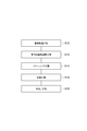
- FIG. 4 is a flowchart illustrating a film forming method according to an embodiment.
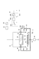
- FIG. 5 is a drawing for explaining the cleaning process shown in FIG. 4, and schematically shows a cross-sectional configuration when the film forming chamber 18 is cut along a plane orthogonal to the extending direction of the first straight portion 44a.
- the load lock chamber 14 and the gate valve 16 are omitted.
- FIG. 6 is a view showing the state of the substrate 12 at the stage where the film forming step S16 shown in FIG. 4 is completed. Like FIG. 5, the substrate 12 is formed on a plane orthogonal to the extending direction of the first straight portion 44a.
- membrane chamber 18 is shown typically.
- the film forming method includes a substrate placement step S10, an indoor atmosphere adjustment step S12, a cleaning step S14, a film forming step S16, and a removal step S18.
- a substrate placement step S10 an indoor atmosphere adjustment step S12
- a cleaning step S14 a cleaning step S14
- a film forming step S16 a removal step S18.
- a removal step S18 a removal step S18.
- the material of the target 34 is described as an oxide semiconductor. Further, the description will be made assuming that the target 34 is already attached to the target holder 36.
- the substrate 12 is placed on the substrate holder 28 in the film forming chamber 18. Specifically, after the substrate 12 is disposed on the substrate holder 22 of the load lock chamber 14, the inside of the load lock chamber 14 is evacuated by the first decompression unit 20 so that the inside of the load lock chamber 14 becomes a high vacuum. At this time, if the inside of the film forming chamber 18 is at atmospheric pressure, the film forming chamber 18 is evacuated by the second decompression unit 26 in this step so as to be a high vacuum.
- the “high vacuum” means a vacuum state of, for example, 5 ⁇ 10 ⁇ 5 Pa or less. The definition of high vacuum is the same below.
- the gate valve 16 is opened, and the substrate 12 is transferred into the film forming chamber 18 by a transfer device (not shown) included in the film forming device 10. 28.
- a transfer device (not shown) included in the film forming device 10. 28.
- the transfer device is, for example, a transfer robot.
- an indoor atmosphere adjustment step S12 for adjusting the atmosphere (or environment) in the film forming chamber 18 to the film forming conditions is performed. Specifically, when the inside of the film forming chamber 18 is not in a high vacuum, the film forming chamber 18 is evacuated by the second decompression unit 26. Thereafter, the valve 24D is opened, and a gas (for example, argon gas) is supplied from the gas supply source 24A into the film forming chamber 18 while the flow rate is controlled by the mass flow controller 24C. At this time, the inside of the film forming chamber 18 is controlled to a predetermined pressure by adjusting the open / close state of the pressure adjusting valve 26C.
- a gas for example, argon gas
- the flow rate of the gas supplied from the gas supply unit 24 into the film forming chamber 18 may be set according to the volume in the film forming chamber 18.
- the predetermined pressure is set to a pressure at which the inductively coupled plasma is easily lit and a characteristic of the oxide semiconductor film becomes a desired characteristic.
- the predetermined pressure is about 0.1 Pa to 10 Pa, and preferably 1 Pa to 3 Pa.
- the cleaning step S14 is performed. Specifically, a high-frequency current is supplied from the high-frequency power source 50 to the antenna 44 via the matching circuit 48 in a state where the sputtering power is not supplied from the power supply unit 40 to the target 34, As shown in FIG. 5, inductively coupled plasma P is generated.
- the generation mechanism of the inductively coupled plasma P is as follows. That is, when a high frequency current is supplied to the antenna 44, an induction electric field is generated by a high frequency magnetic field generated by the high frequency current. Electrons accelerated by the action of the induction electric field ionize the gas supplied from the gas supply unit 24 into the film forming chamber 18, thereby generating inductively coupled plasma P.
- the target surface 34a and the substrate surface 12a are plasma-treated by the inductively coupled plasma P generated as described above to clean the target surface 34a and the substrate surface 12a, that is, the target surface.
- Impurities on the substrate 34a and the substrate surface 12a are removed.
- An example of the impurity is water containing a hydrogen atom.
- the time required for this cleaning may be determined according to the contamination state of the target surface 34a and the like (for example, the adhesion state of impurities etc. on each surface), but is, for example, 5 to 60 seconds, and is a viewpoint of throughput. From about 10 seconds to about 30 seconds is preferable.
- the target surface 34a and the like are cleaned, and then a film forming process S16 for forming a film on the substrate surface 12a is performed.
- the matching circuit 40A is set in a state where the inductively coupled plasma P generated in the cleaning step S14 is maintained, that is, in a state where a high frequency current is supplied from the high frequency power source 50 to the antenna 44 via the matching circuit 48.
- sputtering power is supplied to the target 34 from the AC power supply 40B.
- the power for sputtering may be a power that can impart to the ions the energy generated by the inductively coupled plasma P that can sputter the target 34.
- a film 52 made of an oxide film semiconductor (a material of the target 34) is formed as shown in FIG.
- An example of the film thickness of the film 52 is 20 nm to 100 nm. In such a film thickness, the film 52 is a so-called thin film.
- the substrate 12 on which the film 52 is formed is referred to as a film formation substrate 54.
- a voltage may be applied to the substrate 12 from the bias power supply 30 via the substrate holder 28.
- an extraction step S18 for taking out the film formation substrate 54 from the film formation apparatus 10 is performed. Specifically, after the inside of the film formation chamber 18 is evacuated by the second decompression unit 26, the gate valve 16 is opened, and the film formation substrate 54 is placed on the substrate holder 22 of the load lock chamber 14 by the transfer device. To do. Thereafter, the gate valve 16 is closed and the load lock chamber 14 is leaked to atmospheric pressure, and then the film formation substrate 54 is taken out from the load lock chamber 14.
- the gate valve 16 is closed, and then the load lock chamber 14 is brought to atmospheric pressure. To leak. Then, a new substrate 12 is placed in the load lock chamber 14 and evacuated so that the inside of the load lock chamber 14 becomes a high vacuum. Then, the cleaning step S14 and the film forming step S16 are performed in the film forming chamber 18.
- the film forming step S16 after the film 52 is formed on the substrate 12 in the film forming chamber 18, the film forming substrate 54 is moved to the load lock chamber 14 in the take-out step S16.
- the new substrate 12 in the chamber 14 may be placed on the substrate holder 22 in the film forming chamber 18. That is, a new substrate 12 in the load lock chamber 14 and the film formation substrate 54 may be exchanged.
- the cleaning step S14 is performed as a pretreatment before the film forming step S16, and the inductively coupled plasma P is generated in the cleaning step S14, and the inductively coupled plasma P adheres to the target surface 34a and the like. Impurities are removed.
- the inductively coupled plasma P is used, but since the sputtering power is not supplied to the target 34, the electrons and ions generated by the inductively coupled plasma P are generated on the target surface. Even if it collides with 34a etc., target surface 34a etc. are not sputtered by the above-mentioned electrons and ions.
- the inductively coupled plasma P is generated by supplying a high frequency current to the antenna 44, it takes almost no time to generate the inductively coupled plasma P. Further, since the inductively coupled plasma P has a high density, impurities can be efficiently removed from the target surface 34a and the substrate surface 12a.
- the film forming process S16 is performed after the cleaning process S14, the film 52 in which no impurities are mixed can be formed on the substrate 12. Further, since sputtering of the target 34 also uses high-density inductively coupled plasma P, it can be performed efficiently.
- the target surface 34a and the like are plasma-treated using the inductively coupled plasma P, and impurities attached to the target surface 34a and the like are efficiently removed, and then the film 52 is removed from the substrate surface 12a. Therefore, the deposition substrate 54 in which the entry of impurities into the film 52 is reduced can be manufactured in a shorter time. Therefore, the film 52 can be efficiently formed on the substrate 12, and the throughput when the deposition substrate 54 is manufactured can be improved.
- impurities on the substrate surface 12a are also removed in the cleaning step S14, so that contamination of impurities into the film 52 can be further reduced. Further, for example, even when the plurality of substrates 12 are sequentially transferred to the film formation chamber 18 and the film 52 is formed on the substrate 12, the film 52 with reduced contamination of impurities can be formed on each substrate 12.
- An oxide semiconductor has attracted attention as a material for a thin film in a thin film transistor structure, for example.
- impurities including hydrogen atoms mixed during film formation tend to cause a decrease in reliability of the transistor. Therefore, the above-described film formation method capable of efficiently forming the film 52 with reduced impurity contamination on the substrate 12 is particularly effective when the material of the target 34 includes an oxide semiconductor, and is more reliable. Contributes to the manufacture of thin film transistors.
- the film forming method shown in FIG. 4 is particularly effective when the material of the target 34 includes an amorphous oxide semiconductor such as IGZO. This will be described by taking as an example the case where the material of the target 34 is IGZO.
- the material of the target 34 is also IGZO.
- the target 34 made of such IGZO is used, if the inside of the film forming chamber 18 is exposed to the atmosphere for maintenance, for example, impurities will only adhere to the target surface 34a. In addition, moisture and the like are easily taken into the target 34 as impurities.
- the state (for example, resistance) of the target 34 affects lighting of plasma for sputtering.
- the state (for example, resistance) of the target 34 changes due to the influence of impurities taken into the target 34
- the magnetron sputtering plasma cannot be stably lit. Therefore, before producing a film-formed substrate for a product, it is necessary to return the state of the target 34 to a state before maintenance, that is, a state before being exposed to the atmosphere. Therefore, for example, it is conceivable to perform film formation that does not contribute to a product for a certain time (for example, 1 hour) after maintenance.
- magnetron sputtering has been described as an example, but the same applies to a method in which plasma lighting depends on the state (for example, resistance) of the target 34.
- the inductively coupled plasma P generated by supplying a high frequency current to the antenna 44 is used.
- Plasma P can be generated.
- a process for returning the state of the target 34 to the state before the maintenance is substantially unnecessary. It is. Since the cleaning step S14 is performed as a pretreatment before the film forming step S16, impurities near the target surface 34a are removed, so that the contamination of the impurities into the film 52 on the substrate 12 can be reduced. Therefore, the film 52 in which the mixing of impurities is reduced can be formed on the substrate 12 more efficiently. Therefore, the film forming method is particularly effective when the material of the target 34 includes an amorphous oxide semiconductor such as IGZO.
- the target surface 34a is cleaned by generating inductively coupled plasma P in the film forming chamber 18 without supplying sputtering power to the target 34. Therefore, an impurity removal mechanism for removing impurities on the target surface 34 a, for example, a heating mechanism for the film forming apparatus 10 to heat the target 34 may not be further provided.
- the configuration of the film forming apparatus 10 is simplified and the manufacturing cost is reduced as compared with the case where an impurity removing mechanism is separately provided in the film forming apparatus 10 illustrated in FIG. Therefore, the manufacturing cost of a product manufactured using the film formation substrate 54 is also reduced. Further, in the above film forming method, since there is no need to provide a heating mechanism, there is no influence of distortion caused by heat generated by the heating mechanism, and thus the maintenance of the film forming apparatus 10 is easy.
- both the target surface 34a and the substrate surface 12a are cleaned by inductively coupled plasma P, that is, impurities are removed.
- the cleaning step S14 only the target surface 34a is cleaned. Also good.
- the antenna 44 may be disposed closer to the target 34 between the target 34 and the substrate 12.
- the target surface 34a may be cleaned by supplying power lower than the sputtering power, that is, power that does not cause sputtering, from the power supply unit 40 to the target 34.
- the substrate 12 may be cleaned by applying a voltage that does not sputter the substrate 12 to the substrate holder 28.
- a negative DC voltage may be applied from the DC power supply 40C by switching the switch 40D instead of the AC voltage from the AC power supply 40B.
- the number of antennas 44 for generating the inductively coupled plasma P is not limited to two, and the number of antennas 44 may be one or three or more. Further, the configuration of the antenna 44 is not limited to the illustrated configuration, and any configuration that can generate inductively coupled plasma P for sputtering the target 34 may be used. Further, the configuration of the film forming apparatus 10 is an example, and various modifications can be made without departing from the spirit of the present invention.
Landscapes
- Chemical & Material Sciences (AREA)
- Chemical Kinetics & Catalysis (AREA)
- Engineering & Computer Science (AREA)
- Materials Engineering (AREA)
- Mechanical Engineering (AREA)
- Metallurgy (AREA)
- Organic Chemistry (AREA)
- Physical Deposition Of Substances That Are Components Of Semiconductor Devices (AREA)
- Physical Vapour Deposition (AREA)
Abstract
成膜室18内に配置されたターゲット34にスパッタ用電力を供給しながら誘導結合型プラズマPでターゲットをスパッタリングし、成膜室内においてターゲットに対向して配置された基板12上に膜52を形成する成膜方法であり、ターゲットが配設された成膜室内にターゲットと対向して基板を配置する基板配置工程S10と、ターゲットにスパッタ用電力を供給していない状態において、ターゲットと、基板との間に誘導結合型プラズマを発生させて、ターゲットの表面を誘導結合型プラズマでプラズマ処理することによって、ターゲットの表面をクリーニングするクリーニング工程S14と、ターゲットにスパッタ用電力を供給することで誘導結合型プラズマによってターゲットをスパッタリングし、基板上に膜を形成する成膜工程S16と、を備える。
Description
本発明は、成膜方法に関する。
基板上に膜を形成する成膜技術として、膜となるべき材料からなるターゲットをスパッタリングして、ターゲットに対向して配置された基板上に膜を形成する、いわゆるスパッタリング技術がある。ターゲット表面に、不純物(例えば、水素原子を含む水など)が付着していると、基板に形成される膜に不純物が混入し、成膜済みの基板(以下、成膜基板と称す)を含む製品の信頼性の低下が生じる恐れがある。例えば、高精細ディスプレイ向け薄膜トランジスタ(TFT: thinfilm transistor)における薄膜として酸化物半導体が注目されており、通常、マグネトロンスパッタリング法によって形成されているが、成膜時に混入する水素原子を含む不純物によってトランジスタの信頼性を低下させる要因となっている。
そのため、特許文献1記載の技術では、酸化物半導体からなるターゲットを100℃以上に加熱しながら基板上に膜を形成している。
特許文献1記載の方法では、ターゲットを100℃以上に加熱するために時間を要するため、基板に膜を効率的に形成できない。
そこで、本発明は、基板上に膜を効率的に形成可能な成膜方法を提供することを目的とする。
本発明の一側面に係る成膜方法は、成膜室内に配置されたターゲットにスパッタ用電力を供給しながら誘導結合型プラズマによってターゲットをスパッタリングすることによって、成膜室内においてターゲットに対向して配置された基板上にターゲットの材料からなる膜を形成する成膜方法であって、ターゲットが配設された成膜室内にターゲットと対向して基板を配置する基板配置工程と、ターゲットにスパッタ用電力を供給していない状態において、ターゲットと、基板との間に誘導結合型プラズマを発生させて、ターゲットの表面を誘導結合型プラズマでプラズマ処理することによって、ターゲットの表面をクリーニングするクリーニング工程と、ターゲットにスパッタ用電力を供給することで誘導結合型プラズマによってターゲットをスパッタリングし、基板上に膜を形成する成膜工程と、を備える。
上記方法では、成膜工程の前のクリーニング工程で、成膜室内に誘導結合型プラズマを発生させて、ターゲットの表面をクリーニングしている。なお、「クリーニング」とは、表面上の不純物を除去することである。このクリーニング工程で誘導結合型プラズマを発生させる場合に、ターゲットにスパッタ用電力を供給していないので、誘導結合型プラズマにターゲット表面が曝されても、誘導結合型プラズマで生成される電子及びイオンによって、ターゲットはスパッタリングされない。一方、誘導結合型プラズマで生成される電子及びイオンは、一定のエネルギーを有しているので、ターゲット表面上の水素原子などを含む不純物は誘導結合型プラズマによって除去され、ターゲット表面がクリーニングされる。このクリーニング工程の後に、ターゲットにスパッタ用電力を供給し、誘導結合型プラズマを利用してターゲットをスパッタリングする。このスパッタリングによって、基板上にターゲットの材料からなる膜が形成される。誘導結合型プラズマの発生には時間を要しないと共に、誘導結合型プラズマは高密度であるため、クリーニング工程に要する時間を短縮化できる。その結果、上記成膜方法では、基板上に膜を効率的に形成できる。
一実施形態の上記クリーニング工程では、ターゲットの表面と共に基板の表面を誘導結合型プラズマでプラズマ処理することによって、ターゲットの表面と共に、基板の表面をクリーニングしてもよい。
この場合、基板の表面に付着した不純物も除去されるので、不純物の混入が低減した膜を基板上により確実に形成出来る。
一実施形態において、ターゲットの材料は酸化物半導体を含んでもよい。
酸化物半導体は、例えば、薄膜トランジスタに利用される材料として注目されている。
この薄膜トランジスタでは、膜内の不純物の混入の低減が求められているので、ターゲットの材料が酸化物半導体を含む場合に、上記成膜方法はより有効である。
この薄膜トランジスタでは、膜内の不純物の混入の低減が求められているので、ターゲットの材料が酸化物半導体を含む場合に、上記成膜方法はより有効である。
一実施形態において、上記酸化物半導体は、インジウム、ガリウム、亜鉛、および酸素からなるアモルファス酸化物半導体であってもよい。
上記アモルファス酸化物半導体をターゲットが含む場合、例えば、成膜室をメンテナンスのために大気に曝すと、ターゲット内に不純物が混入しやすい。そのため、例えば、スパッタ用のプラズマの点灯がターゲットの状態に依存するプラズマの場合、ターゲットの状態を、メンテナンス前の状態に戻すための処理を行う必要がある。これに対して、上記成膜方法では、誘導結合型プラズマの点灯には、ターゲットの状態は依存しない。そのため、成膜室を、例えば、メンテナンスしたとしても、メンテナンス後に、プラズマ点灯のためにターゲットの状態をメンテナンス前に戻すための処理が不要である。従って、効率的に、基板に膜を形成することができる。
本発明によれば、効率的に、基板上に膜を形成することができる。
以下、本発明の実施形態について図面を参照しながら説明する。同一の要素には同一符号を付する。重複する説明は省略する。図面の寸法比率は、説明のものと必ずしも一致していない。説明中、「上」、「下」等の方向を示す語は、図面に示された状態に基づいた便宜的な語である。
図1は、一実施形態に係る成膜装置の模式図である。成膜装置10は、基板12上にスパッタリング法によって膜を形成するための装置であり、成膜済みの基板(以下、成膜基板とも称す)を製造する装置でもある。一実施形態において、成膜装置10は、例えば、高精細ディスプレイ用の薄膜トランジスタ(TFT)を製造するためのシステムの一部を構成し得る。
基板12は、成膜基板の使用用途に応じたものであればよい。基板12の例は、液晶ディスプレイ及び有機ELディスプレイなどのフラットパネルディスプレイ、フレキシブルディスプレイ、及び、太陽電池等の半導体デバイスを製造する際に、膜を形成すべき被成膜基板を含む。一実施形態において、基板12は、ベース板上に例えば所定の電極パターン或いは成膜装置10で形成される膜とは別の膜といった所定の構造が形成されたものであり得る。ベース板の材料の例は、ガラス、半導体及びポリイミドフィルムやポリエチレンナフタレート(PEN)フィルム等のプラスチックを含む。基板12は、ベース板自体であってもよい。一実施形態において、成膜装置10が、薄膜トランジスタ(TFT)の製造に適用される場合、基板12の一例は、ベース板としてのガラス板上に、トランジスタの電極(例えば、ゲート電極)となる電極パターンが形成されたものとし得る。
以下の説明において、基板12の表面(以下、基板表面と称す)12aとは、ベース板上に、例えば電極パターン等の所定の構造が形成されている場合は、ベース板上に形成された所定の構造の表面と共に、ベース板の表面(所定の構造が形成されている面)のうち上記所定の構造で覆われていない領域とを含む意味である。なお、ベース板の表面が上記所定の構造で全て覆われている場合は、基板12の表面は、所定の構造の表面に対応する。
成膜装置10は、ロードロック室14と、ゲートバルブ16によってロードロック室14と仕切られており、スパッタリング法によって基板12上に膜を形成するためのスパッタ処理室としての成膜室18とを備える。
ロードロック室14は、成膜室18内に基板12を配置或いは成膜室18内から基板12を取り出す際に成膜室18内を大気に開放しないための真空容器(或いは真空チャンバ)であり、例えば、アルミニウム又はステンレスから構成される。ロードロック室14には、ロードロック室14内を減圧するための第1減圧部20が接続されている。
第1減圧部20は、真空ポンプ20Aを有し、真空ポンプ20Aとロードロック室14とは排気管20Bで接続されている。排気管20Bのうちロードロック室14と真空ポンプ20Aとの間にはバルブ20Cが設けられている。バルブ20Cを開くことで、真空ポンプ20Aとロードロック室14とが連通し、ロードロック室14内を減圧できる状態になる。真空ポンプ20Aの例は、ターボ分子ポンプである。
第1減圧部20は、真空ポンプ20Aの後段(ロードロック室14と反対側に)に、ドライポンプといった真空ポンプが設けられてもよく、真空ポンプ20Aと、その後段の真空ポンプとを接続する排気管にはバルブが設けられてもよい。
ロードロック室14内には、基板ホルダー22が設置されており、基板ホルダー22には、成膜室18に搬送される前の基板12又は成膜室18で膜が形成された後の成膜済みの基板12が配設される。
成膜室18は、成膜室18内に搬送された基板12上に、誘導結合型プラズマを利用したスパッタリングによって基板12上に膜を形成するための真空容器(或いは真空チャンバ)であり、例えば、アルミニウム又はステンレスから構成される。成膜室18には、成膜室18内にガスを供給するためのガス供給部24と、成膜室18内を真空引きするための第2減圧部26とが接続されている。
ガス供給部24は、成膜室18に供給するためのガスが貯留されたガス供給源24Aを有し、ガス供給源24Aは、ガス供給管24Bを介して成膜室18と接続されている。ガス供給源24Aから供給されるガスは、希ガス(例えばアルゴンガス)である。また、成膜室18内で反応性スパッタリングを行う場合は、希ガス(例えばアルゴンガス)と活性ガス(例えば、酸素ガス及び窒素ガスなど)との混合ガスである。一実施形態において、ターゲット34がIGZO(登録商標)からなる場合、ガス供給源24Aから供給されるガスは、アルゴンガスと酸素ガスとの混合ガスである。
ガス供給管24B上には、ガス供給量を調整するためのマスフローコントローラ24Cと、バルブ24Dとが設けられている。バルブ24Dは、マスフローコントローラ24Cに対して上流側(すなわち、成膜室18側)に配置されており、バルブ24Dを開くことで、ガス供給源24Aと成膜室18とが連通し、成膜室18内にガス供給源24Aからマスフローコントローラ24Cdeガス供給量を調整しながら、ガスを供給できる状態になる。
第2減圧部26は、真空ポンプ26Aを有し、真空ポンプ26Aと、成膜室18とは排気管26Bで接続されている。排気管26Bには成膜室18内の圧力を調整するための圧力調整バルブ26Cが設けられている。真空ポンプ26Aの例は、ターボ分子ポンプである。第2減圧部26は、真空ポンプ26Aの後段(成膜室18と反対側に)に、ドライポンプといった真空ポンプが設けられてもよく、真空ポンプ26Aと、その後段の真空ポンプとを接続する排気管にはバルブが設けられてもよい。
成膜室18内には、基板12を保持するための基板ホルダー28が設けられている。一実施形態において、基板ホルダー28には、バイアス電源30からバイアス電圧が印加されてもよい。バイアス電源30と、基板ホルダー28とを電気的に接続する配線は、成膜室18の基板ホルダー22側の壁18aに設けられており真空シール機能を有する絶縁部32によって、成膜室18と絶縁されている。このように、基板ホルダー28にバイアス電圧が印加される場合、基板ホルダー28は導電性を有するが、バイアス電源30が接続されない場合、基板ホルダー28は導電性を有しなくてもよい。
基板ホルダー22と対向する成膜室18の壁18b(図1の構成では、成膜室18の上側の壁、すなわち、天井)には、導電性を有しておりターゲット34を保持するターゲットホルダ36が、真空シール機能を有する絶縁部38を介して取り付けられている。ターゲットホルダ36の例は、バッキングプレートである。
ターゲット34は、ターゲットホルダ36の成膜室18側に保持されている。ターゲット34の材料は、基板表面12aに形成する膜に応じたものであればよく、ターゲット34の材料の例は、石英、アルミナ、酸化物半導体及びZnO(酸化亜鉛)を含む。酸化物半導体の例は、インジウム(Indium)、ガリウム(Gallium)、亜鉛(Zinc)及び酸素(Oxide)から構成されるアモルファス酸化物半導体(In-Ga-Zn-O系酸化物半導体)であるIGZOを含む。ターゲット34の平面視形状は、図3に例示したように、正方形又は長方形といった四角形状でもよいし、円形でもよい。
ターゲット34には、ターゲットホルダ36を介して、電力供給部40が電気的に接続されている。電力供給部40は、成膜室18内に発生される誘導結合型プラズマによってターゲット34をスパッタリングするための電力(以下、スパッタ用電力)をターゲット34に供給するためのものである。電力供給部40は、インピーダンスマッチングのための整合回路40Aを介して交流電圧を印加する交流電源40Bと、ターゲット34に負の直流電圧を印加する直流電源40Cと、それらを切り替えるスイッチ40Dとを備える。交流電源40Bは、後述する高周波電源50が出力する交流電圧よりも低い周波数(例えば、10kHz~100kHz程度)を有する交流電圧を出力する低周波電源でもよく、高周波電源50が出力する交流電圧と同じ周波数の交流電圧を出力する電源でもよい。
成膜室18において、ターゲット34の表面(以下、ターゲット表面と称す)34aと基板表面12aとの間の距離は、例えば、50mm~300mm程度である。
成膜装置10は、成膜室18内に誘導結合型プラズマを発生するためのプラズマ発生装置42を更に有する。図2及び図3を更に利用して、プラズマ発生装置42について説明する。図2は、図1のII-II線に沿った断面構成の模式図である。図3は、図1において、基板12側からターゲット34側をみた場合の図面である。
プラズマ発生装置42は、2本のアンテナ44,44(図1及び図3参照)を有している。各アンテナ44は、U字状を呈する導体であり、所定方向に延在する第1直線部44aと、第1直線部44aの両端から上記所定方向に直交する方向に延在する一対の第2直線部44b,44bとを有する(図2参照)。
アンテナ44は、アンテナ44の両端部が成膜室18の外部に突出するように配置されており、真空シール機能を有する絶縁部46を介して成膜室18の壁18bに固定されている。具体的には、第2直線部44bの第1直線部44aと反対側の端部が成膜室18の外側に突出しており、第2直線部44bを、絶縁部46を介して壁18bに固定することで、アンテナ44は、成膜室18に取り付けられている。
アンテナ44の一端部、すなわち、2つの第2直線部44bのうちの一方の第2直線部44bの端部には、インピーダンスマッチングのための整合回路48を介して、プラズマ発生用の電力供給源としての高周波電源50が電気的に接続されており、アンテナ44の他端部、すなわち、2つの第2直線部44bのうちの一方の第2直線部44bの端部は、接地されている。これにより、高周波電源50からアンテナ44に整合回路48を介して高周波電流を流すことができるようになっている。高周波電源50が出力する高周波電力の周波数、すなわち、アンテナ44に流れる高周波電流の周波数は、例えば、13.56MHzであるが、これに限定されない。
2つのアンテナ44は、これらのアンテナ44に高周波電流が流れることで発生される誘導結合型プラズマに、ターゲット表面34aと基板表面12aが曝されるように、配置されている。アンテナ44の配置例について説明する。
2つのアンテナ44は、第1直線部44aが延在する所定方向及び第2直線部44bの延在方向(ターゲット表面34aの法線方向に対応する)に直交する方向において、2つのアンテナ44の間にターゲット34が位置するように、すなわち、ターゲット34の幅より長い又は上記幅とほぼ同じ距離だけ離して、配置されている。図3に示したように、ターゲット34が四角形状の場合、ターゲット34の対向する一対の辺に、第1直線部44aが平行になるように、アンテナ44は配置され得る。そして、ターゲット表面34aの法線方向或いは基板12の厚さ方向においては、2つのアンテナ44は、ターゲット34と基板12との間のほぼ中央近傍に配置されている。
次に、図4~図6を利用して、上記成膜装置10を利用した成膜方法の一例について説明する。図4は、一実施形態に係る成膜方法を示すフローチャートである。図5は、図4に示したクリーニング工程を説明するための図面であり、第1直線部44aの延在方向に直交する面で成膜室18を切断した場合の断面構成を模式的に示しており、ロードロック室14及びゲートバルブ16を省略して図示している。図6は、図4に示した成膜工程S16が終了した段階での基板12の状態を示す図面であり、図5と同様に、第1直線部44aの延在方向に直交する面で成膜室18を切断した場合の断面構成を模式的に示している。
図4に示すように、一実施形態に係る成膜方法は、基板配置工程S10と、室内雰囲気調整工程S12と、クリーニング工程S14と、成膜工程S16と、取出し工程S18を有する。各工程について説明する。以下では、説明の便宜のため、ターゲット34の材料を酸化物半導体として説明する。また、ターゲット34は既にターゲットホルダ36に取り付けられているとして説明する。
基板配置工程S10では、成膜室18内の基板ホルダー28に基板12を配置する。具体的には、ロードロック室14の基板ホルダー22に基板12を配置した後、第1減圧部20によってロードロック室14内が高真空になるようにロードロック室14内を真空引きする。この際、成膜室18内が大気圧であれば、この工程で成膜室18内を第2減圧部26によって高真空になるように真空引きをしておく。上記「高真空」とは、例えば5×10⁻⁵Pa以下の真空状態を意味する。高真空の定義は、以下同様である。
ロードロック室14内が高真空状態になった後、ゲートバルブ16を開いて、成膜装置10が有する図示しない搬送装置で、基板12を成膜室18内に搬送し、基板12を基板ホルダー28上に配置する。基板12の配置が終了したら、ゲートバルブ16を閉じる。上記搬送装置は、例えば、搬送ロボットである。
ゲートバルブ16を閉じた後、成膜室18内の雰囲気(或いは、環境)を成膜条件に調整するための室内雰囲気調整工程S12を行う。具体的には、成膜室18内が高真空になっていない場合、第2減圧部26によって、成膜室18を真空引きする。その後、バルブ24Dを開いて、マスフローコントローラ24Cで流量を制御しながらガス供給源24Aからガス(例えば、アルゴンガス)を成膜室18内に供給する。この際、圧力調整バルブ26Cの開閉状態を調整することによって、成膜室18内を所定の圧力に制御する。ガス供給部24から成膜室18内に供給するガスの流量は、成膜室18内の容積に応じて設定されていればよい。所定の圧力は、誘導結合型プラズマが点灯しやすい圧力であり、且つ、酸化物半導体膜の特性が所望の特性となるような圧力に設定される。通常、所定の圧力は、0.1Paから10Pa程度であり、好ましくは、1Paから3Paである。
室内雰囲気調整工程S12で、成膜室18内の雰囲気を成膜用の条件に調整した後、クリーニング工程S14を行う。具体的には、ターゲット34に、電力供給部40からスパッタ用電力を供給しない状態で、整合回路48を介して高周波電源50からアンテナ44に高周波電流を供給して、成膜室18内に、図5に示すように、誘導結合型プラズマPを発生させる。
誘導結合型プラズマPの発生のメカニズムは次の通りである。すなわち、アンテナ44に高周波電流が供給されると、高周波電流によって発生する高周波磁界によって誘導電界が生じる。この誘導電界の作用により加速された電子が、ガス供給部24から成膜室18内に供給されたガスを電離させることによって、誘導結合型プラズマPが発生する。
上記のようにして発生させた誘導結合型プラズマPによってターゲット表面34a及び基板表面12a(以下、ターゲット表面34a等とも称す)をプラズマ処理してターゲット表面34a及び基板表面12aをクリーニング、すなわち、ターゲット表面34a及び基板表面12a上の不純物を除去する。不純物の例は、水素原子を含む水である。このクリーニングに要する時間は、ターゲット表面34a等の汚染状況(例えば、各表面への不純物などの付着状況)に応じて決定されればよいが、例えば、5秒から60秒であり、スループットの観点から10秒から30秒程度が好ましい。
一定時間、クリーニング工程S14を行うことで、ターゲット表面34a等をクリーニングした後に、基板表面12aに膜を形成する成膜工程S16を行う。成膜工程S16では、クリーニング工程S14で発生させた誘導結合型プラズマPを維持した状態、すなわち、整合回路48を介して高周波電源50からアンテナ44に高周波電流を供給した状態で、整合回路40Aを介して交流電源40Bからスパッタ用電力をターゲット34に供給する。スパッタ用電力は、誘導結合型プラズマPによって生成されたイオンがターゲット34をスパッタし得るエネルギーを、イオンに付与できる電力であればよい。スパッタ用電力をターゲット34に供給することによって、誘導結合型プラズマP中のイオンがターゲット34をスパッタリングする。その結果、ターゲット34に対向して配置された基板表面12a上に、スパッタ粒子が堆積し、図6に示すように、酸化膜半導体(ターゲット34の材料)からなる膜52が形成される。膜52の膜厚の例は、20nm~100nmであり、このような膜厚の場合、膜52はいわゆる薄膜である。以下、膜52が形成された基板12を成膜基板54と称する。
一実施形態において、成膜工程S16では、基板12に基板ホルダー28を介して、バイアス電源30から電圧を印加していてもよい。
所望の膜厚の膜52を基板表面12aに形成した後、成膜基板54を成膜装置10から取り出す取出し工程S18を行う。具体的には、成膜室18内を、第2減圧部26によって高真空にした後、ゲートバルブ16を開いて、搬送装置によって、成膜基板54をロードロック室14の基板ホルダー22に配置する。その後、ゲートバルブ16を閉じて、ロードロック室14内を大気圧までリークした後、ロードロック室14内から成膜基板54を取り出す。
複数の基板12に順に膜52を形成する場合には、基板配置工程S10において、基板12を成膜室18内に搬送してからゲートバルブ16を閉じた後、ロードロック室14を大気圧にリークする。そして、ロードロック室14に新たな基板12を配置して、ロードロック室14内が高真空になるように真空引きをしておく。そして、成膜室18内でクリーニング工程S14及び成膜工程S16を実施する。成膜工程S16において、成膜室18内の基板12上に膜52を形成した後、取出し工程S16で、成膜基板54をロードロック室14に移動させる際、同時に、搬送装置によって、ロードロック室14の新たな基板12を、成膜室18内の基板ホルダー22に配置すればよい。すなわち、ロードロック室14内の新たな基板12と、成膜基板54とを交換すればよい。
上記方法では、成膜工程S16の前に、前処理としてクリーニング工程S14を実施し、クリーニング工程S14で、誘導結合型プラズマPを発生させ、その誘導結合型プラズマPによって、ターゲット表面34a等に付着している不純物を除去している。このように、クリーニング工程S14では、誘導結合型プラズマPを利用しているが、ターゲット34にスパッタ用電力が供給されていないことから、誘導結合型プラズマPで生成される電子及びイオンがターゲット表面34a等に衝突しても、ターゲット表面34a等は、上記電子及びイオンによってスパッタリングされない。
誘導結合型プラズマPは、アンテナ44に高周波電流を供給することによって生成されるので、誘導結合型プラズマPの生成のためにほとんど時間を要しない。また、誘導結合型プラズマPは高密度であるため、ターゲット表面34a及び基板表面12aから不純物を効率的に除去できる。
クリーニング工程S14の後に、成膜工程S16を実施するため、不純物が混入していない膜52を基板12上に形成可能である。また、ターゲット34のスパッタリングも高密度の誘導結合型プラズマPを利用しているので、効率的に行うことが可能である。
このように、上記成膜方法では、誘導結合型プラズマPを利用してターゲット表面34a等をプラズマ処理し、ターゲット表面34a等に付着した不純物を効率的に除去した後、膜52を基板表面12aに形成しているので、膜52への不純物の混入が低減された成膜基板54を、より短い時間で作製できる。そのため、基板12上に膜52を効率的に形成でき、成膜基板54を作製する際のスループットの向上を図れる。
また、上記成膜方法では、クリーニング工程S14で基板表面12a上の不純物も除去しているので、膜52への不純物の混入が更に低減され得る。また、例えば、複数の基板12を順に成膜室18に搬送して基板12に膜52を形成する場合であっても、各基板12に、不純物の混入が低減された膜52を形成できる。
酸化物半導体は、例えば、薄膜トランジスタの構造中の薄膜の材料として注目されている。薄膜トランジスタでは、成膜時に混入する水素原子を含む不純物がトランジスタの信頼性低下を招きやすい。そのため、不純物の混入が低減された膜52を基板12上に効率的に形成可能な上記成膜方法は、ターゲット34の材料が酸化物半導体を含む場合に特に有効であり、より信頼性の高い薄膜トランジスタの製造に寄与する。
上記図4に示した成膜方法は、ターゲット34の材料がIGZOといったアモルファス酸化物半導体を含む場合に、特に、有効である。この点について、ターゲット34の材料がIGZOである場合を例にして説明する。
基板12上にIGZOかなる膜52を形成する場合、ターゲット34の材料もIGZOである。このようなIGZOからなるターゲット34を使用している際に、成膜室18内を、例えば、メンテナンスなどのために、大気に曝されてしてしまうと、ターゲット表面34aに不純物が付着するのみならず、ターゲット34内にも、水分などが不純物として取り込まれやすい。例えば、基板12上に、IGZOからなる膜を、マグネトロンスパッタリングで形成する場合、ターゲット34の状態(例えば、抵抗)がスパッタ用のプラズマの点灯に影響を与える。そして、上記のように、IGZOからなるターゲット34が、メンテナンス等のために、大気に曝されると、ターゲット34内に取り込まれた不純物の影響によってターゲット34の状態(例えば、抵抗)が変わり、メンテナンス前に設定していたプラズマ点灯の条件では、マグネトロンスパッタ用のプラズマを安定して点灯できない。よって、製品用の、成膜済み基板を作製する前に、ターゲット34の状態を、メンテナンス前の状態、すなわち、大気に曝される前の状態に戻す必要がある。そのため、例えば、メンテナンス後
に、製品に寄与しない成膜を一定時間(例えば、1時間)行うことが考えられる。ここでは、マグネトロンスパッタリングを例にして説明したが、プラズマ点灯がターゲット34の状態(例えば、抵抗)に依存している方法についても同様である。
に、製品に寄与しない成膜を一定時間(例えば、1時間)行うことが考えられる。ここでは、マグネトロンスパッタリングを例にして説明したが、プラズマ点灯がターゲット34の状態(例えば、抵抗)に依存している方法についても同様である。
これに対して、図4に例示した成膜方法では、アンテナ44に高周波電流を供給することで発生する誘導結合型プラズマPを使用しているので、ターゲット34に依存せずに、誘導結合型プラズマPを発生できる。成膜室18のメンテナンス後であっても、クリーニング工程S14において誘導結合型プラズマPを安定して発生させるために、ターゲット34の状態を、メンテナンス前の状態に戻すための処理が実質的に不要である。そして、成膜工程S16の前に、前処理としてクリーニング工程S14を実施することから、ターゲット表面34a近傍の不純物は除去されるので、基板12上の膜52への不純物の混入を低減できる。そのため、より効率的に、不純物の混入が低減された膜52を基板12上に形成することができる。従って、上記成膜方法は、ターゲット34の材料がIGZOといったアモルファス酸化物半導体を含む場合に、特に有効である。
また、図4に示した成膜方法では、ターゲット34にスパッタ用電力を供給しない状態で、成膜室18内に誘導結合型プラズマPを発生させることによって、ターゲット表面34aをクリーニングしている。そのため、ターゲット表面34aの不純物を取り除くための不純物除去機構、例えば、成膜装置10がターゲット34を加熱するための加熱機構を更に有さなくてよい。その結果、図1に例示したような成膜装置10に不純物除去機構を別に設ける場合に比べて、成膜装置10の構成が簡易になり、また、製造コストも低減している。そのため、成膜基板54を用いて製造される製品の製造コストも低減する。また、上記成膜方法では、加熱機構を設ける必要がないので、加熱機構で発生する熱による歪みなどの影響がないので、成膜装置10のメンテナンスも容易である。
ここでは、ターゲット表面34a上の不純物を取り除く場合について説明したが、図4に示した成膜方法では、基板12上の不純物を除去するための不純物除去機構、例えば、基板12を加熱するための加熱機構を別途設けなくてもよい。このように、基板12の不純物除去のための不純物除去機構を別途設けなくてもよいことの作用効果は、ターゲット34の場合と同様であるので、説明を省略する。
以上、本発明の実施形態について説明したが、本発明は上記実施形態に限定されるものではなく、本発明の趣旨を逸脱しない範囲で種々の変更が可能である。
例えば、クリーニング工程S14では、誘導結合型プラズマPで、ターゲット表面34a及び基板表面12aの両方をクリーニング、すなわち、不純物の除去をしているが、クリーニング工程S14では、ターゲット表面34aだけをクリーニングしてもよい。誘導結合型プラズマPが、ターゲット表面34aのみをクリーニングする場合は、アンテナ44は、ターゲット34と基板12との間において、よりターゲット34側に配置されていてもよい。
また、クリーニング工程S14において、ターゲット34に電力供給部40から、スパッタ用電力より低い電力、すなわち、スパッタリングが生じない程度の電力を供給して、ターゲット表面34aをクリーニングしてもよい。また、基板ホルダー28にバイアス電源30が接続されている場合には、基板ホルダー28に、基板12がスパッタリングされない程度の電圧を印加して、基板12をクリーニングしてもよい。
更に、成膜工程S16では、交流電源40Bからの交流電圧の代わりに、スイッチ40Dを切り替えて、直流電源40Cから負の直流電圧を印加してもよい。
誘導結合型プラズマPを発生させるためのアンテナ44の数は2つに限定されず、アンテナ44の数は、1つでもよいし、3つ以上でもよい。また、アンテナ44の構成も例示した構成に限定されず、ターゲット34をスパッタリングするための誘導結合型プラズマPを発生できる構成であればよい。また、成膜装置10の構成は、一例であり、本発明の趣旨を逸脱しない範囲で種々変形が可能である。
12…基板、12a…基板表面、18…成膜室、34…ターゲット、34a…ターゲット表面。
Claims (4)
- 成膜室内に配置されたターゲットにスパッタ用電力を供給しながら誘導結合型プラズマによって前記ターゲットをスパッタリングすることによって、前記成膜室内において前記ターゲットに対向して配置された基板上に前記ターゲットの材料からなる膜を形成する成膜方法であって、
前記ターゲットが配設された前記成膜室内に前記ターゲットと対向して前記基板を配置する基板配置工程と、
前記ターゲットに前記スパッタ用電力を供給していない状態において、前記ターゲットと、前記基板との間に前記誘導結合型プラズマを発生させて、前記ターゲットの表面を前記誘導結合型プラズマでプラズマ処理することによって、前記ターゲットの表面をクリーニングするクリーニング工程と、
前記ターゲットに前記スパッタ用電力を供給することで前記誘導結合型プラズマによって前記ターゲットをスパッタリングし、前記基板上に前記膜を形成する成膜工程と、
を備える成膜方法。 - 前記クリーニング工程では、前記ターゲットの表面と共に前記基板の表面を前記誘導結合型プラズマでプラズマ処理することによって、前記ターゲットの表面と共に、前記基板の表面をクリーニングする、
請求項1記載の成膜方法。 - 前記ターゲットの材料は酸化物半導体を含む、請求項1記載の成膜方法。
- 前記酸化物半導体は、インジウム、ガリウム、亜鉛、および酸素からなるアモルファス酸化物半導体である、請求項3記載の成膜方法。
Applications Claiming Priority (2)
| Application Number | Priority Date | Filing Date | Title |
|---|---|---|---|
| JP2014-092966 | 2014-04-28 | ||
| JP2014092966A JP2015209580A (ja) | 2014-04-28 | 2014-04-28 | 成膜方法 |
Publications (1)
| Publication Number | Publication Date |
|---|---|
| WO2015166605A1 true WO2015166605A1 (ja) | 2015-11-05 |
Family
ID=54358352
Family Applications (1)
| Application Number | Title | Priority Date | Filing Date |
|---|---|---|---|
| PCT/JP2014/082388 Ceased WO2015166605A1 (ja) | 2014-04-28 | 2014-12-08 | 成膜方法 |
Country Status (2)
| Country | Link |
|---|---|
| JP (1) | JP2015209580A (ja) |
| WO (1) | WO2015166605A1 (ja) |
Cited By (1)
| Publication number | Priority date | Publication date | Assignee | Title |
|---|---|---|---|---|
| CN109468604A (zh) * | 2019-01-11 | 2019-03-15 | 郑州大学 | 高透射率igzo薄膜的制备方法 |
Families Citing this family (1)
| Publication number | Priority date | Publication date | Assignee | Title |
|---|---|---|---|---|
| JP2023069790A (ja) * | 2021-11-08 | 2023-05-18 | 株式会社シンクロン | スパッタ成膜装置 |
Citations (6)
| Publication number | Priority date | Publication date | Assignee | Title |
|---|---|---|---|---|
| JPS6376869A (ja) * | 1986-09-19 | 1988-04-07 | Hitachi Ltd | スパツタ装置 |
| WO1989006437A1 (fr) * | 1988-01-11 | 1989-07-13 | Tadahiro Ohmi | Dispositif de formation d'une fine pellicule |
| JPH07180049A (ja) * | 1993-12-22 | 1995-07-18 | Hitachi Ltd | ターゲット表面の清浄化方法 |
| JPH11269643A (ja) * | 1998-03-20 | 1999-10-05 | Toshiba Corp | 成膜装置およびそれを用いた成膜方法 |
| JP2012142495A (ja) * | 2011-01-05 | 2012-07-26 | Ulvac Japan Ltd | プラズマエッチング方法及びプラズマエッチング装置 |
| JP2012222176A (ja) * | 2011-04-11 | 2012-11-12 | Dainippon Printing Co Ltd | 薄膜トランジスタ及びその製造方法 |
-
2014
- 2014-04-28 JP JP2014092966A patent/JP2015209580A/ja active Pending
- 2014-12-08 WO PCT/JP2014/082388 patent/WO2015166605A1/ja not_active Ceased
Patent Citations (6)
| Publication number | Priority date | Publication date | Assignee | Title |
|---|---|---|---|---|
| JPS6376869A (ja) * | 1986-09-19 | 1988-04-07 | Hitachi Ltd | スパツタ装置 |
| WO1989006437A1 (fr) * | 1988-01-11 | 1989-07-13 | Tadahiro Ohmi | Dispositif de formation d'une fine pellicule |
| JPH07180049A (ja) * | 1993-12-22 | 1995-07-18 | Hitachi Ltd | ターゲット表面の清浄化方法 |
| JPH11269643A (ja) * | 1998-03-20 | 1999-10-05 | Toshiba Corp | 成膜装置およびそれを用いた成膜方法 |
| JP2012142495A (ja) * | 2011-01-05 | 2012-07-26 | Ulvac Japan Ltd | プラズマエッチング方法及びプラズマエッチング装置 |
| JP2012222176A (ja) * | 2011-04-11 | 2012-11-12 | Dainippon Printing Co Ltd | 薄膜トランジスタ及びその製造方法 |
Cited By (1)
| Publication number | Priority date | Publication date | Assignee | Title |
|---|---|---|---|---|
| CN109468604A (zh) * | 2019-01-11 | 2019-03-15 | 郑州大学 | 高透射率igzo薄膜的制备方法 |
Also Published As
| Publication number | Publication date |
|---|---|
| JP2015209580A (ja) | 2015-11-24 |
Similar Documents
| Publication | Publication Date | Title |
|---|---|---|
| EP3711078B1 (en) | Linearized energetic radio-frequency plasma ion source | |
| US7977255B1 (en) | Method and system for depositing a thin-film transistor | |
| CN102187010B (zh) | 薄膜形成方法以及场效应晶体管的制造方法 | |
| CN106715750A (zh) | 成膜方法及溅镀装置 | |
| CN107622945A (zh) | 等离子体蚀刻方法、等离子体蚀刻装置和基板载置台 | |
| US20240347327A1 (en) | Semiconductor processing tool and methods of operation | |
| CN104073769A (zh) | 膜形成方法 | |
| JP2008069402A (ja) | スパッタリング装置及びスパッタリング方法 | |
| CN104282567B (zh) | 制造igzo层和tft的方法 | |
| JP2015209580A (ja) | 成膜方法 | |
| JP2000268994A (ja) | 高周波グロー放電を利用した表面処理方法 | |
| CN103219214B (zh) | 连续式系统的等离子体制程、设备、腔体及机构 | |
| KR20180028949A (ko) | 플라스마 에칭 방법 | |
| CN115565872A (zh) | 半导体器件的制造方法 | |
| CN1904133B (zh) | 溅射装置和溅射方法 | |
| JP2009246392A (ja) | 基板処理装置 | |
| TW201708587A (zh) | 用於在濺射沉積製程期間支撐至少一個基板的載具、用於在至少一個基板上濺射沉積的設備以及用於在至少一個基板上濺射沉積的方法 | |
| CN105931960A (zh) | 一种刻蚀掺铝氧化锌薄膜的方法 | |
| JP4364335B2 (ja) | スパッタリング装置 | |
| WO2017194088A1 (en) | Method and apparatus for vacuum processing | |
| KR100645038B1 (ko) | 기판 유효 면적을 극대화한 스퍼터링 장치 | |
| TWI845143B (zh) | 電漿處理裝置 | |
| JP3180557U (ja) | 薄膜作製装置 | |
| JP2007092095A (ja) | 薄膜形成方法及び薄膜形成装置 | |
| JPH09190899A (ja) | プラズマ処理方法及びその装置 |
Legal Events
| Date | Code | Title | Description |
|---|---|---|---|
| 121 | Ep: the epo has been informed by wipo that ep was designated in this application |
Ref document number: 14891017 Country of ref document: EP Kind code of ref document: A1 |
|
| NENP | Non-entry into the national phase |
Ref country code: DE |
|
| 122 | Ep: pct application non-entry in european phase |
Ref document number: 14891017 Country of ref document: EP Kind code of ref document: A1 |