WO2015163036A1 - 荷電粒子線装置及びその帯電除去方法 - Google Patents
荷電粒子線装置及びその帯電除去方法 Download PDFInfo
- Publication number
- WO2015163036A1 WO2015163036A1 PCT/JP2015/057616 JP2015057616W WO2015163036A1 WO 2015163036 A1 WO2015163036 A1 WO 2015163036A1 JP 2015057616 W JP2015057616 W JP 2015057616W WO 2015163036 A1 WO2015163036 A1 WO 2015163036A1
- Authority
- WO
- WIPO (PCT)
- Prior art keywords
- sample
- charged particle
- particle beam
- wafer
- beam apparatus
- Prior art date
- Legal status (The legal status is an assumption and is not a legal conclusion. Google has not performed a legal analysis and makes no representation as to the accuracy of the status listed.)
- Ceased
Links
Images











Classifications
-
- H—ELECTRICITY
- H01—ELECTRIC ELEMENTS
- H01J—ELECTRIC DISCHARGE TUBES OR DISCHARGE LAMPS
- H01J37/00—Discharge tubes with provision for introducing objects or material to be exposed to the discharge, e.g. for the purpose of examination or processing thereof
- H01J37/02—Details
- H01J37/20—Means for supporting or positioning the object or the material; Means for adjusting diaphragms or lenses associated with the support
-
- H—ELECTRICITY
- H01—ELECTRIC ELEMENTS
- H01J—ELECTRIC DISCHARGE TUBES OR DISCHARGE LAMPS
- H01J37/00—Discharge tubes with provision for introducing objects or material to be exposed to the discharge, e.g. for the purpose of examination or processing thereof
- H01J37/02—Details
- H01J37/22—Optical, image processing or photographic arrangements associated with the tube
-
- H—ELECTRICITY
- H01—ELECTRIC ELEMENTS
- H01J—ELECTRIC DISCHARGE TUBES OR DISCHARGE LAMPS
- H01J37/00—Discharge tubes with provision for introducing objects or material to be exposed to the discharge, e.g. for the purpose of examination or processing thereof
- H01J37/26—Electron or ion microscopes; Electron or ion diffraction tubes
- H01J37/28—Electron or ion microscopes; Electron or ion diffraction tubes with scanning beams
-
- H—ELECTRICITY
- H10—SEMICONDUCTOR DEVICES; ELECTRIC SOLID-STATE DEVICES NOT OTHERWISE PROVIDED FOR
- H10P—GENERIC PROCESSES OR APPARATUS FOR THE MANUFACTURE OR TREATMENT OF DEVICES COVERED BY CLASS H10
- H10P72/00—Handling or holding of wafers, substrates or devices during manufacture or treatment thereof
- H10P72/70—Handling or holding of wafers, substrates or devices during manufacture or treatment thereof for supporting or gripping
Definitions
- the present invention relates to a charged particle beam apparatus used for measuring and inspecting a sample and a method for removing the charge.
- the observation surface of the semiconductor wafer is required to be flat.
- electrostatic chucks are widely used in which a voltage is applied to a semiconductor wafer through a dielectric layer on the surface to generate an electrostatic force and the semiconductor wafer is held on the wafer holding surface by the electrostatic force.
- the semiconductor wafer is not electrically connected to the outside. For this reason, there is a concern about the influence of the progress of global charging of the semiconductor wafer caused by the current irradiated for observation on the performance (for example, imaging quality). Further, when residual adsorption occurs due to charging, there arises a problem that the semiconductor wafer cannot be normally removed from the wafer holding surface.
- Patent Document 1 A technique for solving this problem is disclosed in Patent Document 1.
- the abstract of Patent Document 1 states that “One embodiment of the present invention relates to a method of releasing a semiconductor wafer that is in electrical contact with a surface of an electrostatic chuck by a trapping voltage. In this method, the trapping voltage is released. For a period after this release, the first region of the wafer is lifted from the surface of the electrostatic chuck by a first distance while the second region of the wafer is kept in close contact with the surface of the electrostatic chuck. The predetermined condition is monitored, and when the predetermined condition is met, the second region is lifted from the surface of the electrostatic chuck. " It is described.
- Patent Document 1 a method of discharging a semiconductor wafer by contacting a ground contact from the upper side of the semiconductor wafer, a protrusion of a contact pin inserted from the back surface of the semiconductor wafer, and electrically contacting the semiconductor wafer.
- a method of discharging a semiconductor wafer by contacting a ground contact from the upper side of the semiconductor wafer, a protrusion of a contact pin inserted from the back surface of the semiconductor wafer, and electrically contacting the semiconductor wafer.
- static elimination There are known methods for static elimination.
- Patent Document 1 the method described in Patent Document 1 is intended to safely take out the semiconductor wafer after all the process processing is completed, and does not take into account the charge removal during the processing of the semiconductor wafer. For this reason, the method of the cited document 1 cannot cope with the influence of the charging during the observation of the semiconductor wafer on the observation screen. In addition, the charge removal method using the contact pin cannot be discharged because it is not conductive depending on the type of the insulating film on the back surface. Further, if the contact pins are pressed against the semiconductor wafer with a strong force in order to ensure conduction, there is a problem of damaging the back surface of the semiconductor wafer.
- the inventors adopt, for example, the configuration described in the claims.
- the present specification includes a plurality of means for solving the above-described problems.
- “the sample is lifted from the electrostatic chuck between the time when the sample is loaded into the sample chamber and the time when the sample is unloaded. It is characterized by a charged particle beam apparatus that performs a set of an ascending operation and a descending operation for placing the lifted sample on the electrostatic chuck again.
- FIG. 1 is a diagram illustrating a schematic configuration of a charged particle beam apparatus according to Embodiment 1.
- FIG. 3 is a diagram showing a schematic cross-sectional configuration of a sample holding mechanism in Embodiment 1.
- FIG. 2 is a diagram showing a schematic top configuration of a sample holding mechanism in Embodiment 1.
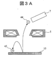
- FIG. 3 is a diagram illustrating the trajectory of secondary electrons according to the first embodiment. The figure explaining the relationship between a wafer surface potential and the brightness of a secondary electron image. The figure explaining the conduction
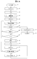
- FIG. 5 is a flowchart illustrating a recipe execution process in the first embodiment.
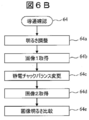
- the flowchart which shows a continuity confirmation process.
- the flowchart which shows a static elimination process.
- the figure which shows the example of the setting screen (GUI) of a static elimination function.
- FIG. 3 is a diagram illustrating a schematic configuration of a charged particle beam apparatus according to a second embodiment.
- FIG. 5 is a diagram showing a schematic cross-sectional configuration of a sample holding mechanism in Embodiment 2.
- FIG. 6 is a diagram for explaining a trajectory of secondary electrons according to the second embodiment. The figure explaining the relationship between secondary electron energy and the number of secondary electrons generated. The figure explaining the relationship between the intensity
- FIG. 10 is a flowchart showing a recipe execution process in Embodiment 2. The flowchart which shows an electrification measurement process.
- FIG. 10 is a diagram for explaining a wafer surface potential correction operation in the second embodiment.
- FIG. 6 is a diagram illustrating a schematic configuration of a charged particle beam apparatus according to a third embodiment. 10 is a flowchart illustrating a recipe execution process according to the third embodiment.
- the charged particle beam apparatus widely includes an apparatus that captures an image of a sample using a charged particle beam.
- an inspection apparatus using a scanning electron microscope, a review apparatus, and a pattern measurement apparatus can be given.
- the present invention can be applied to a sample observation apparatus using various ions, a sample processing apparatus using a charged particle beam, and a sample analysis apparatus.
- the charged particle beam device includes a system in which the above charged particle beam devices are connected by a network and a composite device of the above charged particle beam devices.
- a semiconductor wafer on which a pattern is formed hereinafter referred to as “wafer”
- the sample in the present invention is not limited to a semiconductor wafer.
- FIG. 1 shows a schematic configuration example of a scanning electron microscope.
- the microscope main body includes a column 1 and a sample chamber 2 which are electron optical systems.
- the column 1 includes an electron gun 3, a condenser lens 4, an objective lens 5, a deflector 6, a secondary electron detector 7, an E ⁇ B filter 8, and a reflected electron detector 9.
- the primary electron beam (irradiated electrons) generated from the electron gun 3 is converged by the condenser lens 4 and the objective lens 5 and irradiates the wafer 10 placed on the electrostatic chuck 11.
- the primary electron beam is deflected by the deflector 6 and scans along the surface of the wafer 10.
- the deflection of the primary electron beam by the deflector 6 is controlled in accordance with a signal given from the beam scanning controller 16.
- the configuration of the optical system is not limited to the above-described configuration, and may include, for example, other lenses, electrodes, and detectors, or a part of the configuration may be different from the above configuration.
- the XY stage 12 installed in the sample chamber 2 moves the position of the wafer 10 relative to the column 1 within the XY plane (within a horizontal plane) according to a control signal given from the stage controller 17.
- a standard sample 13 for beam calibration is attached on the XY stage 12.
- the scanning electron microscope has an optical microscope 14 for wafer alignment. Detection signals output from the secondary electron detector 7 and the backscattered electron detector 9 are sent to the image processing board 18 and imaged.
- the wafer 10 is loaded into the sample chamber 2 through the load lock chamber 15.
- the load lock chamber 15 is kept in a vacuum state like the column 1 and the sample chamber 2.
- the loading of the wafer 10 from the external space at atmospheric pressure to the sample chamber 2 in the vacuum state is called loading, and on the contrary, the unloading of the wafer 10 from the sample chamber 2 to the external space at atmospheric pressure is unloaded. Call it.
- the operation of the entire microscope is controlled by the computer 19.
- FIGS. 2A and 2B show a schematic configuration of a sample holding mechanism constituted by the electrostatic chuck 11.
- the wafer 10 is held on the upper surface of the electrostatic chuck 11.
- a positive electrode 33 and a negative electrode 34 are embedded in the electrostatic chuck 11, and a positive potential Vp is applied to the positive electrode 33 and a negative potential Vn is applied to the negative electrode 34 during electrostatic chucking.
- An electrostatic force is generated by applying both potentials, and the wafer 10 is attracted and held on the electrostatic chuck 11 by the generated electrostatic force.
- no potential is applied to the positive electrode 33 and the negative electrode 34 during periods other than the electrostatic chuck (for example, during loading or unloading).
- the electrostatic chuck 11 of the present embodiment has a structure capable of applying a retarding voltage Vr.
- the symbols indicating the power supplies in the figure indicate that the applied voltage can be varied.
- the electrostatic chuck 11 is provided with one hole that accommodates the conductive contact pin 35 and reaches the surface from the back surface of the electrostatic chuck 11.
- the contact pin 35 includes a contact pin made of a conductive material and a spring mechanism (not shown).
- the tip of the contact pin is hemispherical or conical.
- the contact pins are pressed against the back surface of the wafer 10 with a weak force by a spring mechanism so as to always contact the wafer 10 placed on the electrostatic chuck 11.
- the contact by the push-up force ensures conduction between the tip of the contact pin and the back surface of the wafer 10. However, if this pushing force is too strong, the back surface of the wafer 10 will be damaged.
- the scanning electron microscope of this embodiment has a charge eliminating function other than the contact pins 35. The static elimination function will be described later.
- each electrode and the wafer 10 The following electrical relationship is established between each electrode and the wafer 10.
- the capacitance of the capacitor formed by the positive electrode 33 and the wafer 10 is Cp
- the capacitance of the capacitor formed by the negative electrode 34 and the wafer 10 is Cn
- the surface potential of the wafer 10 is V. Even if there is no conduction between the wafer 10 and the contact pin 35, when the wafer 10 is not charged, the charges stored in the two capacitors are equal, and therefore, the following relational expression holds. Note that the offset voltage ⁇ V is zero.
- V ⁇ Cp * (Vp + Vr) + Cn * (Vr + Vn)) / (Cp + Cn) (2)
- Cp Cn
- the lift mechanism is used to temporarily lift the wafer 10 from the mounting surface of the electrostatic chuck 11 when the wafer 10 is loaded, unloaded, or during static elimination such as during observation, which is proposed in this embodiment.
- the lift mechanism is composed of three lift pins 36a to 36c and a drive mechanism 37 (for example, a motor).
- the three lift pins 36a to 36c are arranged at equal angular intervals in the circumferential direction of the electrostatic chuck 11. In the example of FIG. 2B, they are arranged 120 degrees apart. With this arrangement, the wafer 10 is held by the lift pins 36a to 36c at three positions on the back surface side at positions lifted from the surface of the electrostatic chuck 11.
- the electrostatic chuck 11 is formed with three holes for accommodating the three lift pins 36a to 36c. Each hole reaches the surface from the back surface of the electrostatic chuck 11.
- the tip portions (contact surfaces with the wafer 10) of the lift pins 36a to 36c are substantially flat, and at least the tip portions are formed of an elastic conductor. This conductor is always connected to ground potential. However, the entire lift pins 36a to 36c need not be conductors. Further, the tip portions of the lift pins 36a to 36c (contact surfaces with the wafer 10) need not be entirely conductive.
- the structure of the lift pins may be different from that described in the present embodiment as long as the tip of the lift pins that are in contact with the wafer is an elastic conductor and connected to the ground. For example, a donut-shaped elastic conductor may be disposed at the tip end portions (contact surfaces with the wafer 10) of the lift pins 36a to 36c.
- the conductor having elasticity is, for example, conductive rubber. By having elasticity, it is considered important that the contact surface of the conductive elastic body is deformed when it comes into contact with the wafer and the contact area is increased.
- the inventors attach an elastic conductor having a donut shape having an outer diameter (diameter) of 8 mm and a conductor width of 2 mm to the tip of the lift pins 36a to 36c, and the thickness of the oxide film on the back surface of the wafer 10 is 500 nm. In the case of, it was confirmed that there was a static elimination effect.
- the drive mechanism 37 operates to lift the tip portions of the lift pins 36a to 36c upward by about 3 mm from the mounting surface of the electrostatic chuck 11 at least during static elimination. It should be noted that when the tip portions of the lift pins 36 a to c push up the electrostatic chuck 11, the force that contacts the back surface of the electrostatic chuck 11 is greater than the force that the contact pin 35 contacts the back surface of the electrostatic chuck 11.
- FIG. 3A shows the trajectory of the secondary electrons 44 generated in the vicinity of the surface of the wafer 10 by the irradiation of the primary electron beam.
- the secondary electrons 44 are detected as secondary electron signals by the secondary electron detector 7 in the objective lens 5.
- the secondary electrons 45 generated near the surface of the wafer 10 are pulled back to the wafer 10 by an electric field and are not detected by the secondary electron detector 7.
- FIG. 3B shows the brightness (vertical axis) of the secondary electron image formed by arranging the secondary electron signal in accordance with the scanning position of the primary electron beam, and the surface potential (horizontal axis) of the wafer 10. Showing the relationship.
- a curve 46 represents a relationship in which the brightness of the secondary electron image starts to gradually decrease when the surface potential V of the wafer 10 becomes positive, and becomes almost zero when it exceeds a certain potential.
- This method for confirming the presence or absence of conduction is a method for confirming whether or not the contact pins 35 and the wafer 10 are in a conduction state.
- the surface potential V of the wafer 10 is always kept at a constant retarding voltage Vr ( ⁇ 0), so the wafer 10 is not charged and the charge removal process is executed. It is unnecessary.
- This confirmation method of the presence / absence of conduction is used to determine whether or not it is necessary to execute a charge removal process.
- V (Vp + Vn) / 2 + Vr + ⁇ V Equation (4)
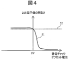
- the horizontal axis of FIG. 4 indicates the offset potential of the electrostatic chuck 11.
- the brightness of the secondary electron image is a negative potential as shown by the curve 51.
- the offset potential ⁇ V increases beyond a certain potential, the brightness of the secondary electron image becomes almost zero.
- the shape of the curve 51 is the same as the curve 46 shown in FIG. 3B.
- the surface potential V of the wafer 10 is always equal to the retarding voltage Vr.
- Vr is a negative potential, the brightness of the secondary electron image is always the same brightness without depending on the offset potential ⁇ V, as indicated by a straight line 52 (indicated by a dotted line).
- the brightness of the secondary electron image varies greatly depending on the presence or absence of conduction between the wafer 10 and the contact pins 35.
- the ratio between the brightness of the secondary electron image when the offset potential ⁇ V is 0 V and the brightness of the secondary electron image when +10 V is applied to the offset potential ⁇ V is used. Based on this, the presence / absence of conduction between the wafer 10 and the contact pins 35 is determined. The determination process based on the brightness ratio of the secondary electron image is executed by the computer 19 based on a predetermined program.
- a curve 53 (solid line) in FIG. 5A is a brightness characteristic of the secondary electron image with respect to the offset potential ⁇ V of the electrostatic chuck when the wafer 10 is not charged.
- the wafer 10 is observed with a high acceleration voltage of 3 kV or more, the irradiated electrons reach the inside of the wafer, and the ratio of the amount of secondary electrons to the amount of irradiated electrons is as small as 0.2 or less. For this reason, the wafer 10 is negatively charged by the electrons accumulated inside the wafer. If the charge amount accumulated on the wafer 10 is Q, the following relationship is established.
- Cp * ⁇ (Vp + Vr) ⁇ V ⁇ + Q Cn * ⁇ V ⁇ (Vr + Vn) ⁇ (5)
- V ⁇ Cp * (Vp + Vr) + Cn * (Vr + Vn)) / (Cp + Cn) + Q / (Cp + Cn) (6)
- V 0 Q / (Cp + Cn) depending on the charge amount Q accumulated in the wafer 10.
- a curve 54 (dotted line) indicates the brightness characteristic of the secondary electron image with respect to the electrostatic chuck potential when the wafer 10 is negatively charged by V 0 . Since the wafer 10 is negatively charged, the range in which the secondary electron image appears bright is shifted to the range where the offset potential ⁇ V is positive.
- FIG. 5B shows the relationship between the wafer observation time and the wafer charge amount.
- the horizontal axis represents the wafer observation time
- the vertical axis represents the wafer charge amount.
- the wafer observation time becomes long, the wafer charge amount exceeds the allowable value for obtaining the required accuracy.
- a periodic charge removal operation is necessary.
- the time change of the wafer charge amount becomes a continuous line 56 (solid line) indicated by a sawtooth pattern.
- the pattern represented by the continuous line 56 is the effect of the charge removal process proposed in this embodiment.
- FIG. 6A shows a processing procedure of the recipe processing (step 61) proposed in the present embodiment.
- the recipe processing is executed by the computer 19 by reading a recipe (a program in which settings for specifying measurement conditions and inspection conditions, parameters, various commands, and the like are registered) from a storage area (not shown).
- the computer 19 loads the wafer 10 to be observed into the sample chamber 2 (step 62), and starts measuring the wafer observation time T when the loading is completed (step 63).
- the computer 19 performs continuity confirmation for determining whether or not a static elimination operation is necessary (step 64). Details of the conduction process will be described later. In the case where an insulating film is formed on the back surface of the wafer 10, conduction by the contact pins 35 is not ensured.
- the computer 19 executes wafer alignment using an optical microscope image and an SEM (Scanning Electron Microscope) image (step 65).
- the alignment is a process of associating the wafer coordinate system with the coordinate system of the apparatus with reference to a pre-registered pattern position.
- the computer 19 moves to the first designated point set in the recipe and takes a secondary electron image (step 66).
- the computer 19 determines whether or not imaging for all designated points set in the recipe has been completed (step 67). If imaging has been completed for all designated points, the wafer 10 is removed. Unloading is performed (step 75), and the recipe is terminated (step 76).
- the computer 19 determines the presence / absence of continuity (in other words, the necessity of charge removal) based on the determination result in the continuity confirmation step (step 64) (step 68). If continuity is ensured (in the case of OK), there is no need for static elimination, so the computer 19 returns to the process of step 66 and continues imaging all the remaining designated points. On the other hand, if the continuity is not ensured (for NG), the computer 19 determines whether the wafer observation time T exceeds the predetermined value T 0 (step 69).
- the specified value T 0 is a threshold value that gives a static elimination cycle.
- step 70 the computer 19 executes a static elimination process (step 70). Details of the charge removal process will be described later.
- the computer 19 After the charge removal process, the computer 19 resets the wafer observation time T to zero (step 71) and executes realignment of the wafer 10 (step 72). Thereafter, the computer 19 compares the realignment result with the alignment result in step 65, and determines whether or not the positional deviation of the wafer 10 exceeds a specified value (step 73). This is because in the static elimination process, the wafer 10 is moved up and down by several millimeters with respect to the wafer placement surface by the lift pins 36a to 36c, so that there is a possibility that the wafer 10 may be misaligned when it is placed again on the wafer placement surface.
- step 74 the computer 19 once unloads the wafer 10 into the atmosphere, reloads it onto the stage of the electrostatic chuck 11 (step 74), and executes the alignment of step 72 again. To do. If the amount of deviation in step 73 is less than or equal to the specified value, the computer 19 returns to the processing in step 66.
- step 64a the computer 19 adjusts the gain of the detection system circuit so that the brightness of the secondary electron image acquired with the offset potential ⁇ V set to 0 V is appropriate (step 64a), and the first image Is acquired (step 64b).
- step 64c the computer 19 changes the balance (offset potential ⁇ V) of the electrostatic chuck 11 so that the wafer surface potential becomes +10 V (step 64c), and acquires the second image without changing the gain of the detection system. (Step 64d).
- the computer 19 compares the brightness of the two images, and determines that the continuity is NG if the average brightness of the second image is 50% or less of the average brightness of the first image. If it is greater than 50%, it is determined that conduction is OK (step 64e).
- this determination method is an example.
- step 70a the computer 19 controls the voltage application to the electrostatic chuck 11 to be turned off.
- step 70b the computer 19 lifts up the wafer 10 by 3 mm from the surface of the electrostatic chuck 11 using the lift pins 36a to 36c (step 70b).
- This operation is merely a lift-up operation and does not involve the discharge of atmospheric pressure to the external space as in the case of unloading.
- an elastic conductor connected to the ground potential supports (contacts) the back surface (insulating film) of the wafer 10.
- the inventors experimented that the insulating film formed on the back surface of the wafer 10 can be neutralized when an O-ring having a diameter of about 8 mm and a width of 2 mm is used at the tip of each lift pin with respect to an oxide film having a thickness of 500 nm. It is confirmed by.
- the computer 19 lifts the wafer 10 down and places it again on the surface of the electrostatic chuck 11 (step 70c). Subsequently, the computer 19 applies a voltage (a positive potential Vp to the static electrode 33 and a negative potential Vn to the negative electrode 34) to the electrostatic chuck 11 (step 70d). As a result, the wafer 10 is again attracted to the surface of the electrostatic chuck 11.
- FIG. 7 shows an example of a static elimination function setting screen mounted on the scanning electron microscope according to the embodiment.
- the GUI (Graphical User Interface) 81 has a map display area 82, an image display area 83, an image acquisition position display area 84, and a wafer charge removal setting area 85.
- the map display area 82 either a wafer map or a chip map is selectively displayed.
- the map is switched by selecting the wafer map selection button 82a and the chip map selection button 82b.
- a mouse (not shown) is used.
- the image display area 83 either an optical microscope image or an SEM image is selectively displayed.
- the image is switched by a selection operation of the optical microscope image selection button 83a and the SEM image selection button 83b.
- the display magnification of the image display area 83 can be changed by a magnification change button 83c. Further, image acquisition can be instructed by operating the image acquisition button 83d.
- the image acquisition condition is set after the image condition setting window is launched by operating the image condition setting button 83e.
- the image acquisition position is specified by the in-chip coordinates and the image acquisition chip.
- the chip map is displayed in the map display area 82 by the chip map selection button 82b.
- the pointer is moved to an arbitrary position on the chip map and the mouse is clicked, an image of the clicked place is acquired.
- an image is clicked in the image display area, the location is registered as an image acquisition coordinate, and an image acquisition position corresponding to the image acquisition position display area 84 is added.
- an initial state only the origin chip (0, 0) is selected as the image acquisition chip.
- the wafer map is selected on the wafer map while the wafer map is displayed by the wafer map selection button 82a.
- the wafer neutralization function under observation is enabled by checking the check box 85a in the wafer neutralization setting area 85. Further, the interval for executing the wafer neutralization (specified value T 0 used in step 69) can be changed by inputting a numerical value in units of minutes in the static elimination interval setting box 85b.
- At least tip portions (contact surfaces with the wafer 10) of the lift pins 36a to 36c are flat, and an elastic conductor connected to the ground potential is attached. If continuity between the wafer 10 and the contact pin 35 is confirmed (NO in step 68), there is no need for periodic charge removal, and therefore no unnecessary charge removal operation is performed.
- This embodiment has a function of automatically performing static elimination for each specified value T 0 registered based on the relationship between the wafer observation time measured in advance and the wafer charge amount (step 69).
- the wafer 10 is lifted and lifted a plurality of times from the loading to the unloading of the wafer 10.
- the throughput decreases. Is minimal.
- the user can specify whether or not to perform the charge removal and the time interval at the time of execution using the setting screen shown in FIG. In this setting, the user can set the static elimination timing based on the brightness of the secondary electron image displayed in the image display area 83.
- FIG. 8 shows a schematic configuration example of a scanning electron microscope according to the second embodiment.
- parts corresponding to those in FIG. The only difference between the configuration shown in FIG. 8 and the configuration shown in FIG. 1 is that an energy filter 20 is added to the column 1.
- Other configurations are basically the same as those of the first embodiment.
- the energy filter 20 is disposed on the passage path of secondary electrons between the E ⁇ B filter 8 and the reflected electron detector 9. In the case of the present embodiment, it is assumed that the contact pin 35 is not provided on the electrostatic chuck 11.
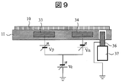
- FIG. 9 shows a schematic configuration of the sample holding mechanism used in this embodiment.
- the sample holding mechanism of the present embodiment is not provided with the contact pin 35. For this reason, it is necessary to always remove the charge during the execution of the recipe regardless of whether or not the insulating layer is formed on the back surface of the wafer 10.
- Other configurations of the sample holding mechanism are the same as those of the sample holding mechanism (FIG. 2) of the first embodiment.
- -1000 V is applied as the retarding voltage Vr.
- the surface potential V of the wafer 10 is given by the following equation.
- the surface potential V of the wafer 10 is ⁇ 1000V.
- the extraction voltage from the electron gun 3 is set to 11 kV, and the wafer 10 having the surface potential V of ⁇ 1000 V is irradiated with electrons at 10 kV.
- FIG. 10A secondary electrons generated in the vicinity of the surface of the wafer 10 by the primary electron beam are detected by the secondary electron detector 7 as a detection signal.
- the energy filter 20 has a characteristic that the secondary electrons 95 with high energy are allowed to pass through and the secondary electrons 96 with low energy are returned to the wafer 10 side.
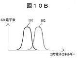
- FIG. 10B is a graph in which the vertical axis represents the number of secondary electrons and the horizontal axis represents the secondary electron energy.
- a curve 101 indicates the energy distribution of secondary electrons when the wafer 10 is not charged. When the wafer 10 is negatively charged, the secondary electrons are further accelerated upward by the electric field, so that the energy distribution of the secondary electrons is shifted to the high energy side as indicated by the curve 102. That is, the shift amount is proportional to the charge amount of the wafer 10.
- FIG. 10C is a graph in which the vertical axis indicates the brightness of the secondary electron image and the horizontal axis indicates the intensity of the energy filter 20, and the curves 103 and 104 indicate the characteristics of the brightness of the secondary electron image with respect to the energy filter intensity. ing.
- the right side of the horizontal axis indicates that the absolute value of the negative potential applied to the energy filter 20 is large.
- a curve 103 is a characteristic of the brightness of the secondary electron image with respect to the strength of the energy filter 20 when the wafer 10 is not charged. As shown by the curve 103, when the strength of the energy filter 20 is increased (the negative potential to be applied is increased), the secondary electron image becomes darker from the point in time, and the potential of the energy filter 20 is ⁇ V 0 [V].
- the brightness of the image decreases to 1 ⁇ 2 of the brightness when the intensity of the energy filter 20 is 0V.
- a curve 104 is a characteristic when the wafer 10 is negatively charged. In the curve 104, the characteristic is shifted to the right by the charged potential. For this reason, the brightness when the potential of the energy filter 20 is ⁇ V 1 [V] decreases to 1 ⁇ 2 of the brightness when the strength of the energy filter 20 is 0V.
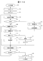
- FIG. 11A shows the processing procedure of the recipe processing (step 101) proposed in this embodiment.
- the recipe process is executed by the computer 19 by reading a recipe (a program in which measurement conditions and inspection conditions are registered) from a storage area (not shown).
- the computer 19 loads the wafer 10 to be observed into the sample chamber 2 (step 102).
- the computer 19 executes wafer alignment using the optical microscope image and the SEM image after the loading is completed (step 103). This is because in this embodiment, since there is no contact pin 35 in the sample holding mechanism, confirmation of continuity is unnecessary.
- the computer 19 moves to the first designated point set in the recipe (step 104). Subsequently, the computer 19 determines whether or not the designated point of the movement destination is the first point (step 105). In the case of the first point, the computer 19 measures the initial charge amount of the wafer 10 (step 106) and registers the measured value as an energy filter reference value (step 107). Details of the measurement process will be described later. Further, the energy filter reference value is an energy filter intensity at which the secondary electron intensity is halved, and corresponds to ⁇ V 0 [V] in FIG. 10C.
- the computer 19 determines whether or not it is a charging measurement point (step 108).
- the charging measurement point is set in advance in the recipe. For example, when the charging measurement is set to be performed every 10 points, the computer 19 determines whether the designated point for imaging is the 10th point, the 20th point, the 30th point, or the like. Do. If it is determined that the measurement point is a charge measurement point, the computer 19 performs charge measurement (step 109). Details of the charge measurement will be described later. Thereafter, the computer 19 determines whether or not the measured charge amount is greater than or equal to a threshold value (step 110). In this embodiment, the charging threshold is 50V. Of course, the threshold value is not limited to this value.
- the computer 19 drives and controls the lift pins 36a to 36c to lift up the wafer 10 from the mounting surface of the electrostatic chuck 11 and then lift down the wafer 10 to lift it up. Is removed (step 111).
- the static elimination operation does not include an unload operation.
- the computer 19 instructs execution of alignment (step 112).
- the computer 19 executes charge correction using the retarding voltage Vr (step 113).
- the retarding potential Vr is changed by + 20V
- the potential at the surface of the electrostatic chuck 11 is changed to ⁇ 980V
- the surface potential V of the wafer 10 is returned to ⁇ 1000V.
- the corrected surface potential V is the potential at the start of measurement.
- the retarding potential Vr is automatically changed to the initial value.
- the computer 19 captures a secondary electron image of the designated point (step 114). Thereafter, the computer 19 determines whether or not imaging has been completed for all designated points specified in the recipe (step 115). If the designated points remain, the computer 19 moves to step 104 and becomes the next designated point. Move the imaging area. On the other hand, if all the imaging points specified by the recipe have been completed, the computer 19 unloads the wafer 10 from the sample chamber 2 (step 116) and ends the recipe (step 117).
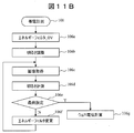
- FIG. 11B explains the detailed operation of the charge measurement executed in steps 106 and 109.
- the computer 19 sets the energy filter to 0 V (step 106a) and adjusts the brightness of the image (step 106b). Thereafter, the computer 19 acquires a secondary electron image (106c) and measures the average brightness of the secondary electron image (step 106d).
- the computer 19 determines whether or not the energy filter setting value is the final stage of the variable range (step 106e). If not, the computer 19 changes the setting of the energy filter 20 to the next setting value. After that (step 106f), the process returns to step 106c to acquire a secondary electron image for the next set value. This operation is repeated until a positive result is obtained in step 106e. By this iterative process, energy filter strength and brightness characteristic data of the secondary electron image as shown in FIG. 10C are acquired.
- the computer 19 calculates the surface potential V of the wafer 10 from the acquired characteristic data.
- the surface potential V of the wafer 10 is obtained as an energy filter intensity at which the brightness of the secondary electron image is 50% of the initial value (the brightness of the secondary electron image at the energy filter 0V).
- the method of obtaining the surface potential V of the wafer 10 is not limited to this method, and may be calculated as, for example, the energy filter strength at a certain brightness other than 50% of the initial value.
- the charging measurement may be terminated when the brightness of the secondary electron image becomes 50% or less of the initial value.
- the charge measurement may be speeded up by continuously changing the energy filter strength.
- FIG. 12 illustrates an operation for correcting the surface potential V of the wafer 10 according to this embodiment, which is executed during the execution of the recipe.
- FIG. 12 shows how the charge measurement value (step 106g), the retarding voltage, and the wafer surface potential change.
- the surface potential of the wafer 10 gradually changes to a negative potential due to beam irradiation as indicated by the continuous line 121, and returns to 0V when the charge removal is executed.
- the reason why the continuous line 121 changes in a staircase pattern is to perform charging measurement at every 10 imaging points in the present embodiment, and the width of each staircase corresponds to the imaging time of 10 times.
- the initial value of the retarding potential in this embodiment is set to ⁇ 1000 V.
- the continuous line 122 representing the retarding voltage Vr increases stepwise. For example, if ⁇ V measured in step 109 (step 106g) is ⁇ 10V, the retarding voltage Vr is corrected to ⁇ 990V. Further, as shown in FIG. 12, when the charged potential of the wafer 10 returns to 0V due to static elimination, the retarding voltage Vr also returns to ⁇ 1000V. It should be noted that the surface potential V of the wafer 10 gradually increases with every imaging until the charge measurement is executed, and thus changes to a sawtooth shape as indicated by the continuous line 123. Note that the surface potential V of the wafer 10 returns to ⁇ 1000 V every time the charge is measured by charge correction (correction of the retarding voltage Vr) without performing the charge removal process.
- the following technical effects are realized in addition to the basic effects of the first embodiment.
- the brightness of the secondary electron image immediately after loading the wafer 10 is measured and set as a reference value, and the reference value and the brightness of the secondary electron image measured periodically are determined.
- static elimination is automatically executed (step 111). For this reason, an efficient static elimination process can be executed without reducing the throughput as much as possible.
- the surface potential of the wafer 10 can be measured by acquiring a plurality of secondary electron images while changing the energy filter strength as described with reference to FIG. 11B.
- the surface potential of the wafer 10 may be calculated from the recipe conditions (acceleration voltage, irradiation current, image capturing time, etc.).
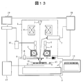
- FIG. 13 shows a schematic configuration example of a scanning electron microscope according to the third embodiment.
- parts corresponding to those in FIG. The only difference between the configuration shown in FIG. 13 and the configuration shown in FIG. 1 is that a charged electrometer 21 is added to the side surface of the column 1.
- the charging potentiometer 21 measures the charging potential of the wafer 10 in a non-contact manner.
- Other configurations are basically the same as those of the first embodiment. However, the configuration of the sample holding mechanism assumes a case where the contact pin 35 is not provided on the electrostatic chuck 11 as in the second embodiment.
- FIG. 14 shows the processing procedure of the recipe processing (step 131) proposed in this embodiment.
- the recipe process is also executed by the computer 19 by reading the recipe from a storage area (not shown).
- the computer 19 loads the wafer 10 to be observed into the sample chamber 2 (step 132).
- the computer 19 executes wafer alignment using the optical microscope image and the SEM image after the loading is completed (step 133). This is because in this embodiment, since there is no contact pin 35 in the sample holding mechanism, confirmation of continuity is unnecessary.
- the computer 19 moves to the designated point of the first recipe and takes a secondary electron image of the designated point (step 134). Thereafter, the computer 19 determines whether or not imaging of all designated points has been completed (step 135). When the imaging of all the designated points has been completed, the computer 19 unloads the wafer 10 from the sample chamber 2 (step 146) and ends the recipe (step 147).
- the computer 19 measures the charged potential of the wafer 10 by the charged potentiometer 21 (step 136). Each time the charging potential is measured for a new designated point, the computer 19 determines whether or not the charging potential exceeds “threshold 1” (step 137). If the charging potential is within “threshold 1”, the computer 19 returns to step 134 and images the next designated point. On the other hand, when the charged potential exceeds “threshold value 1”, the computer 19 executes a charge removal process (step 138). The charge removal process is the same process as in the first embodiment.
- the computer 19 again measures the charged potential at the same designated point (step 139), and determines whether or not the charge potential after the charge removal becomes smaller than “threshold 2” (step 140). If the charged potential is equal to or greater than “threshold 2” even after static elimination, the computer 19 forcibly ends the operation of the recipe, and displays on the GUI that the static elimination could not be executed normally (step 141). For example, the occurrence of an error is notified. On the other hand, when the charge potential after static elimination becomes smaller than “threshold value 2”, the computer 19 executes realignment of the wafer 10 (step 142), and the wafer position change amount with respect to the alignment immediately after the wafer loading is within a specified value. Whether or not (step 143).
- the computer 19 adjusts the wafer position by moving the wafer 10 to the load chamber in a vacuum and then returning it to the stage of the electrostatic chuck 11 (step 144). Thereafter, realignment is performed (step 145).
- “Threshold 1” is set to ⁇ 50 and V, and “Threshold 2” is set to ⁇ 25V.
- the set value is not limited to this.
- “threshold 1” and “threshold 2” may be the same.
- the “threshold value” of the wafer position change amount is set to 1 mm. However, this value may be in a range where the observation of the edge portion on the electrostatic chuck 11 and the unloading operation are normally performed.
- the present invention is not limited to the configuration of the embodiment described above, and includes various modifications.
- the existing lift pins 36a to 36c are connected to the ground potential and used for static elimination, but a static elimination dedicated pin may be provided separately from the existing lift pins.
- the present invention does not necessarily have all the configurations described in the above-described embodiments.
- a part of a certain embodiment can be replaced with the configuration of another embodiment, and the configuration of another embodiment can be added to the configuration of a certain embodiment. It is also possible to add other configurations to the configuration of each embodiment, replace a partial configuration of each embodiment with another configuration, or delete a partial configuration of each embodiment.
- each of the above-described configurations, functions, processing units, processing means, and the like may be partly or entirely realized as, for example, an integrated circuit or other hardware.
- Information such as recipes (programs), tables, and files executed by the computer 19 should be stored in a storage device such as a memory, a hard disk, an SSD (Solid State Drive), or a storage medium such as an IC card, an SD card, or a DVD. Can do.
- Control lines and information lines indicate what is considered necessary for the description, and do not represent all control lines and information lines necessary for the product. In practice, it can be considered that almost all components are connected to each other.
- SEM image selection button 83c Magnification change button 83d ... Image acquisition button 83e ... Image condition setting Button 84 ... Image acquisition position display area 85 ... Wafer charge removal setting area 85a ... Check box 85b ... Charge removal interval setting box
Landscapes
- Chemical & Material Sciences (AREA)
- Analytical Chemistry (AREA)
- Container, Conveyance, Adherence, Positioning, Of Wafer (AREA)
- Testing Or Measuring Of Semiconductors Or The Like (AREA)
Abstract
本発明の荷電粒子線装置のウェハリフト機構(36,37)は、試料(10)が試料室内にロードされてからアンロードされるまでの間に、試料を静電チャック(11)から持ち上げる上昇動作と、持ち上げられた試料を再び静電チャックに載置する下降動作とを少なくとも1回実行することにより、試料の帯電を除去する機能を有する。これにより、スループットの低下は最小限とした効率的かつ安価な除電技術を提供できる。
Description
本発明は、試料の計測検査等に使用される荷電粒子線装置とその帯電除去方法に関する。
近年における半導体デバイスの微細化と三次元化の進行に伴い、アスペクト比の大きい深穴及び深溝の底の観察や計測が求められている。また、微細化により、異なる工程間でのパターンの重ね合わせの管理の重要度が高まっている。このような深穴若しくは深溝の底、又は、デバイス内部の観察では、荷電粒子を高い加速電圧で照射する必要がある。また、同構造の観察では、表面の観察時に比べ、試料から出力される二次電子及び反射電子が少なくなる。このため、従来手法に比べて高い照射電流が要求される。
加えて、半導体ウェハの観察では、観察面が平坦であることが要求される。このため、表面の誘電層を介して半導体ウェハに電圧を印加して静電気力を発生させ、当該静電気力により半導体ウェハをウェハ保持面に保持する静電チャックが広く使われている。ところが、静電チャックでは、半導体ウェハが電気的に外部と導通されない。このため、観察のために照射される電流に起因する半導体ウェハのグローバルな帯電の進行が、性能面(例えば撮像品質)に与える影響が懸念される。また、帯電により残留吸着が発生すると、半導体ウェハをウェハ保持面から正常に離脱できない問題が生じる。
この問題を解決する手法が、特許文献1に開示されている。特許文献1の要約部には、「本発明の一実施形態は、静電チャックの表面に捕捉電圧によって電気的に密着している半導体ウェハを解放する方法に関する。本方法では、捕捉電圧を解除する。この解除後のある期間、ウェハの第2の領域を静電チャックの表面に密着させたまま、ウェハの第1の領域を静電チャックの表面から第1の距離だけ持ち上げる。期間中、所定の条件をモニタする。所定の条件が満たされると、第2の領域を静電チャックの表面から持ち上げる。」
と記載されている。
と記載されている。
なお、特許文献1以外にも、半導体ウェハの上方側からアースコンタクトを接触させて半導体ウェハを除電する方法、半導体ウェハの裏面からコンタクトピンの突起部を挿し、半導体ウェハと電気的に接触させて除電する方法が知られている。
ところが、特許文献1に記載されている方法は、全てのプロセス処理が終了した後に、半導体ウェハを安全に取りだすことを意図するものであり、半導体ウェハの処理中における帯電除去は考慮されていない。このため、引用文献1の手法は、半導体ウェハの観察中における帯電が観察画面に与える影響には対応できない。また、コンタクトピンを用いる除電方法は、裏面の絶縁膜の種類によっては導通が取れず除電できない。また、導通を確保するために、強い力でコンタクトピンを半導体ウェハに押し当てると、半導体ウェハの裏面にダメージを与える問題がある。
上記課題を解決するため、発明者らは、例えば請求の範囲に記載の構成を採用する。本明細書は上記課題を解決する手段を複数含んでいるが、その一例を挙げるならば、「試料が試料室内にロードされてからアンロードされるまでの間に、試料を静電チャックから持ち上げる上昇動作と、持ち上げた試料を再び静電チャックに載置する下降動作を一組とする動作を実行する荷電粒子線装置」を特徴とする。
本発明により、試料の検査中や計測中にも、試料を破壊することなく除電でき、帯電に起因する画質の低下を防いで常に安定した検査、計測等を実現することができる。前述した以外の課題、構成及び効果は、以下の実施の形態の説明により明らかにされる。
以下では、荷電粒子線装置の一例として走査型電子顕微鏡について説明する。ただし、走査型電子顕微鏡は、本発明の単なる一例であり、本発明は以下に説明する実施の形態に限定されるものではない。本発明において荷電粒子線装置とは、荷電粒子線を用いて試料の画像を撮像する装置を広く含むものとする。荷電粒子線装置の一例として、走査型電子顕微鏡を用いた検査装置、レビュー装置、パターン計測装置が挙げられる。また、各種イオンを用いた試料観察装置、さらには荷電粒子線を用いる試料加工装置や試料解析装置にも適用可能である。また、以下の説明において、荷電粒子線装置とは、上記の荷電粒子線装置がネットワークで接続されたシステムや上記の荷電粒子線装置の複合装置も含むものとする。また、以下では、パターンが形成された半導体ウェハ(以下「ウェハ」という)を試料として用いる場合について説明するが、本発明における試料は、半導体ウェハに限られるものではない。
[実施例1]
[装置構成]
図1に、走査型電子顕微鏡の概略構成例を示す。顕微鏡本体は、電子光学系であるカラム1と試料室2で構成される。カラム1の内部には、電子銃3、コンデンサレンズ4、対物レンズ5、ディフレクタ6、2次電子検出器7、E×Bフィルタ8、反射電子検出器9が含まれる。電子銃3から発生された一次電子線(照射電子)は、コンデンサレンズ4と対物レンズ5により収束され、静電チャック11上に載置されたウェハ10を照射する。一次電子線は、ディフレクタ6により偏向され、ウェハ10の表面に沿って走査する。ディフレクタ6による一次電子線の偏向は、ビーム走査コントローラ16から与えられる信号に従って制御される。
[装置構成]
図1に、走査型電子顕微鏡の概略構成例を示す。顕微鏡本体は、電子光学系であるカラム1と試料室2で構成される。カラム1の内部には、電子銃3、コンデンサレンズ4、対物レンズ5、ディフレクタ6、2次電子検出器7、E×Bフィルタ8、反射電子検出器9が含まれる。電子銃3から発生された一次電子線(照射電子)は、コンデンサレンズ4と対物レンズ5により収束され、静電チャック11上に載置されたウェハ10を照射する。一次電子線は、ディフレクタ6により偏向され、ウェハ10の表面に沿って走査する。ディフレクタ6による一次電子線の偏向は、ビーム走査コントローラ16から与えられる信号に従って制御される。
一次電子線の照射によりウェハ10から発生した2次電子は、E×Bフィルタ8によって2次電子検出器7の方向に向けられ、2次電子検出器7で検出される。また、ウェハ10からの反射電子は、反射電子検出器9によって検出される。なお、光学系の構成は、前述の構成に限られず、例えば他のレンズ、電極、検出器を含んでもよいし、一部の構成が上記の構成と異なっていてもよい。
試料室2に設置されるXYステージ12は、ステージコントローラ17から与えられる制御信号に従い、カラム1に対してウェハ10の位置をXY面内(水平面内)で移動させる。XYステージ12上には、ビーム校正のための標準試料13が取り付けられている。また、走査型電子顕微鏡は、ウェハアライメントのための光学顕微鏡14を有している。2次電子検出器7及び反射電子検出器9から出力される検出信号は、画像処理ボード18に送られ画像化される。ウェハ10は、ロードロック室15を通じて試料室2にロードされる。なお、ロードロック室15は、カラム1及び試料室2と同様に真空状態に保たれている。本明細書では、大気圧の外部空間から真空状態の試料室2へのウェハ10の搬入をロードと呼び、その反対に、試料室2から大気圧の外部空間へのウェハ10の搬出をアンロードと呼ぶ。また、顕微鏡全体の動作は、コンピュータ19により制御される。
図2A及びBに、静電チャック11で構成される試料保持機構の概略構成を示す。前述したように、ウェハ10は、静電チャック11の上面に保持される。静電チャック11には、正電極33と負電極34が埋め込まれており、静電チャック時、正電極33には正電位Vpが印加され、負電極34には負電位Vnが印加される。両電位の印加により静電気力が発生し、発生した静電気力によりウェハ10が静電チャック11に吸着保持される。なお、静電チャック以外の期間では(例えばロード時やアンロード時)、正電極33と負電極34に対する電位の印加は無い。また、本実施例の静電チャック11には、リターディング電圧Vrの印加が可能な構造となっている。図中の電源を示す記号は、いずれも印加電圧を可変できることを表している。
静電チャック11には、導電性を有するコンタクトピン35を収容し、静電チャック11の裏面から表面に達する1つの孔が設けられている。コンタクトピン35は、導電性材料のコンタクトピンと不図示のばね機構とで構成されている。コンタクトピンの先端は半球面又は円錐形成である。コンタクトピンは、静電チャック11に載置されたウェハ10と常に接触するように、ばね機構による弱い力でウェハ10の裏面に押し付けられる。この押し上げ力による接触により、コンタクトピンの先端とウェハ10の裏面との導通が確保される。ただし、この押し上げ力が強すぎると、ウェハ10の裏面にダメージを与えてしまう。また、前述したように、ウェハ10の裏面に絶縁膜が形成されている場合には、コンタクトピンによる接触によっては、ウェハ10の裏面との間に導通を確保できない。導通が確保できない場合には、一次電子線の照射中にウェハ10が帯電するため、本実施例の走査型電子顕微鏡には、コンタクトピン35以外の除電機能が用意されている。除電機能については後述する。
各電極とウェハ10との間には以下に示す電気関係が成立する。ここでは、正電極33とウェハ10で形成されるキャパシタの静電容量をCp、負電極34とウェハ10で形成されるキャパシタの静電容量をCn、ウェハ10の表面電位をVとする。ウェハ10とコンタクトピン35の導通がなくても、ウェハ10が帯電していない場合、2つのキャパシタに蓄えられる電荷は等しいため、以下の関係式が成り立つ。なお、オフセット電圧ΔVはゼロとしている。
Cp*{(Vp+Vr)-V}=Cn*{V-(Vr+Vn)} …式(1)
厳密な意味では、他に存在する浮遊容量の影響が考えられるが、それらはCnやCpに比較して十分に小さく、計算式において省略しても問題ない。
Cp*{(Vp+Vr)-V}=Cn*{V-(Vr+Vn)} …式(1)
厳密な意味では、他に存在する浮遊容量の影響が考えられるが、それらはCnやCpに比較して十分に小さく、計算式において省略しても問題ない。
式(1)を、ウェハ10の表面電位Vに対して展開すると、以下の式が得られる。
V={Cp*(Vp+Vr)+Cn*(Vr+Vn))/(Cp+Cn) …式(2)
静電チャック11において、Cp=Cnであるとすると、以下の関係式が成り立つ。
V=(Vp+Vn)/2+Vr …式(3)
V={Cp*(Vp+Vr)+Cn*(Vr+Vn))/(Cp+Cn) …式(2)
静電チャック11において、Cp=Cnであるとすると、以下の関係式が成り立つ。
V=(Vp+Vn)/2+Vr …式(3)
リフト機構は、ウェハ10のロード時、アンロード時、本実施例で提案する観察中等の除電時に、ウェハ10を静電チャック11の載置面から一時的に持ち上げるために使用される。本実施例の場合、リフト機構は、3本のリフトピン36a~cとその駆動機構37(例えばモータ)で構成される。3本のリフトピン36a~cは、静電チャック11の円周方向に等角度ずつ離して配置される。図2Bの例では120°ずつ離して配置される。この配置により、ウェハ10は、その裏面側の3点において、静電チャック11の表面から持ち上げられた位置でリフトピン36a~cにより保持される。なお、静電チャック11には、3本のリフトピン36a~cを収容する3つの孔が形成されている。各孔は、静電チャック11の裏面から表面に達する。
リフトピン36a~cの先端部(ウェハ10との接触面)はほぼ平坦であり、少なくとも当該先端部は弾性を有する導電体で形成されている。この導電体は、アース電位に常に接続されている。もっとも、リフトピン36a~cの全体が導電体である必要はない。また、リフトピン36a~cの先端部(ウェハ10との接触面)についても、その全体が導電体である必要はない。リフトピンのウェハとの接触部分である先端部が弾性導電体でかつアースに接続されていれば、リフトピンの構造は本実施例で記載したものと異なっていてもよい。例えばリフトピン36a~cの先端部(ウェハ10との接触面)には、ドーナツ形状の弾性を有する導電体が配置されていても良い。ここで弾性を有する導電体とは例えば導電性ゴム等である。弾性を有することにより、ウェハと接触したときに導電性弾性体の接触面が変形して、接触面積が大きくなることが重要と考えられる。発明者らは、リフトピン36a~cの先端部に、外径(直径)が8mm、導体の幅が2mmのドーナツ形状を有する弾性導電体を取り付け、ウェハ10の裏面の酸化膜の厚さが500nmの場合に除電効果があることを確認した。また、駆動機構37は、少なくとも除電時に、リフトピン36a~cの先端部分を、静電チャック11の載置面から3mmほど上方に持ち上げるように動作する。なお、リフトピン36a~cの先端部分が静電チャック11を押し上げる際に静電チャック11の裏面に接触する力は、コンタクトピン35が静電チャック11の裏面に接触する力よりも大きい。
[ウェハ表面電位と二次電子像の明るさとの関係]
図3Aに、一次電子線の照射によりウェハ10の表面近傍で生じた二次電子44の軌道を示す。二次電子44は、対物レンズ5内の2次電子検出器7により二次電子信号として検出される。なお、対物レンズ5に対してウェハ10が正の電位を有する場合、ウェハ10の表面近傍で生じた二次電子45は、電界によりウェハ10へ引き戻され、2次電子検出器7において検出されなくなる。図3Bには、二次電子信号を一次電子線の走査位置に応じて配置することにより形成される2次電子像の明るさ(縦軸)と、ウェハ10の表面電位(横軸)との関係を示している。曲線46は、ウェハ10の表面電位Vが正になると、2次電子画の明るさが徐々に低下し始め、やがてある電位を超えるとほぼゼロになる関係を表している。
図3Aに、一次電子線の照射によりウェハ10の表面近傍で生じた二次電子44の軌道を示す。二次電子44は、対物レンズ5内の2次電子検出器7により二次電子信号として検出される。なお、対物レンズ5に対してウェハ10が正の電位を有する場合、ウェハ10の表面近傍で生じた二次電子45は、電界によりウェハ10へ引き戻され、2次電子検出器7において検出されなくなる。図3Bには、二次電子信号を一次電子線の走査位置に応じて配置することにより形成される2次電子像の明るさ(縦軸)と、ウェハ10の表面電位(横軸)との関係を示している。曲線46は、ウェハ10の表面電位Vが正になると、2次電子画の明るさが徐々に低下し始め、やがてある電位を超えるとほぼゼロになる関係を表している。
[導通有無の確認方法]
次に、図4を用い、本実施例において提案する導通有無の確認方法について説明する。この導通有無の確認方法は、コンタクトピン35とウェハ10とが導通状態にあるか否かを確認するための方法である。なお、導通が確認されている場合には、ウェハ10の表面電位Vは常に一定のリターディング電圧Vr(<0)に保たれるため、ウェハ10が帯電することはなく、除電処理の実行は不要である。この導通有無の確認方法は、除電処理の実行が必要であるか否かを判定するために使用される。図4の横軸は式(3)で示される表面電位Vに相当する電位であり、縦軸は2次電子像の明るさである。本実施例では、リターディング電圧Vrを固定電位とし、VpとVnにオフセット電位ΔVを加える。すなわち、正電極33にはVp+ΔVを印加し、負電極34にはVn+ΔVを印加する。これらオフセット電位ΔVを加味した電位を、式(3)のVpとVnに代入すると、次式が得られる。
V=(Vp+Vn)/2+Vr+ΔV …式(4)
ここで、Vp=-Vn、Vr=0Vとすると、ウェハ10の表面電位Vはオフセット電位ΔVとなる。このため、図4の横軸には、静電チャック11のオフセット電位と示している。
次に、図4を用い、本実施例において提案する導通有無の確認方法について説明する。この導通有無の確認方法は、コンタクトピン35とウェハ10とが導通状態にあるか否かを確認するための方法である。なお、導通が確認されている場合には、ウェハ10の表面電位Vは常に一定のリターディング電圧Vr(<0)に保たれるため、ウェハ10が帯電することはなく、除電処理の実行は不要である。この導通有無の確認方法は、除電処理の実行が必要であるか否かを判定するために使用される。図4の横軸は式(3)で示される表面電位Vに相当する電位であり、縦軸は2次電子像の明るさである。本実施例では、リターディング電圧Vrを固定電位とし、VpとVnにオフセット電位ΔVを加える。すなわち、正電極33にはVp+ΔVを印加し、負電極34にはVn+ΔVを印加する。これらオフセット電位ΔVを加味した電位を、式(3)のVpとVnに代入すると、次式が得られる。
V=(Vp+Vn)/2+Vr+ΔV …式(4)
ここで、Vp=-Vn、Vr=0Vとすると、ウェハ10の表面電位Vはオフセット電位ΔVとなる。このため、図4の横軸には、静電チャック11のオフセット電位と示している。
ここで、ウェハ10とコンタクトピン35の間に導通がない場合(ウェハ10の裏面が絶縁膜の場合)、2次電子像の明るさは曲線51に示すように、オフセット電位ΔVが負の電位から正の電位に入った時点から徐々に減少し、オフセット電位ΔVがある電位を超えて大きくなると2次電子像の明るさはほぼゼロになる。この曲線51の形状は、図3Bに示す曲線46と同様である。一方、ウェハ10とコンタクトピン35との間で導通が確保されている場合、ウェハ10の表面電位Vは、常にリターディング電圧Vrと等しくなる。ここで、Vrは負の電位であるので、2次電子像の明るさは、直線52で示されるように(点線で示す)、オフセット電位ΔVに依存せずに常に同じ明るさとなる。
図4から分かるように、静電チャックのオフセット電位ΔVとして正電位を印加した状態では、ウェハ10とコンタクトピン35との間の導通の有無により2次電子像の明るさが大きく異なる。本実施例では、この明るさの違いに着目し、オフセット電位ΔVが0Vの時の2次電子像の明るさと、オフセット電位ΔVに+10Vを印加した時の2次電子像の明るさとの比率に基づいて、ウェハ10とコンタクトピン35との導通の有無を判定する。この2次電子像の明るさの比率に基づく判定処理は、コンピュータ19が所定のプログラムに基づいて実行する。
[帯電と帯電補正]
次に、図5A及びBを用い、本実施例による帯電補正の様子を説明する。図5Aの曲線53(実線)は、ウェハ10が帯電していない時の静電チャックのオフセット電位ΔVに対する2次電子像の明るさの特性である。3kV以上の高い加速電圧でウェハ10を観察した場合、照射電子がウェハ内部まで到達するため、照射電子量に対する2次電子量の割合は0.2以下と小さくなる。このため、ウェハ内部に蓄積した電子によりウェハ10が負に帯電する。ウェハ10に蓄積される電荷量をQとすると、以下の関係が成立する。
Cp*{(Vp+Vr)-V}+Q=Cn*{V-(Vr+Vn)} …式(5)
次に、図5A及びBを用い、本実施例による帯電補正の様子を説明する。図5Aの曲線53(実線)は、ウェハ10が帯電していない時の静電チャックのオフセット電位ΔVに対する2次電子像の明るさの特性である。3kV以上の高い加速電圧でウェハ10を観察した場合、照射電子がウェハ内部まで到達するため、照射電子量に対する2次電子量の割合は0.2以下と小さくなる。このため、ウェハ内部に蓄積した電子によりウェハ10が負に帯電する。ウェハ10に蓄積される電荷量をQとすると、以下の関係が成立する。
Cp*{(Vp+Vr)-V}+Q=Cn*{V-(Vr+Vn)} …式(5)
式(5)をVについて展開すると、次式となる。
V={Cp*(Vp+Vr)+Cn*(Vr+Vn))/(Cp+Cn)+Q/(Cp+Cn)…式(6)
式(6)より、ウェハ10に蓄積される電荷量Qによって、ウェハ10の表面電位VがV0=Q/(Cp+Cn)だけシフトすることが分かる。ここで、曲線54(点線)は、ウェハ10が負極性にV0だけ帯電した場合の静電チャック電位に対する2次電子像の明るさ特性を示している。ウェハ10が負極性に帯電しているため、オフセット電位ΔVが正の電位の範囲まで、2次電子像が明るく見える範囲がシフトする。
V={Cp*(Vp+Vr)+Cn*(Vr+Vn))/(Cp+Cn)+Q/(Cp+Cn)…式(6)
式(6)より、ウェハ10に蓄積される電荷量Qによって、ウェハ10の表面電位VがV0=Q/(Cp+Cn)だけシフトすることが分かる。ここで、曲線54(点線)は、ウェハ10が負極性にV0だけ帯電した場合の静電チャック電位に対する2次電子像の明るさ特性を示している。ウェハ10が負極性に帯電しているため、オフセット電位ΔVが正の電位の範囲まで、2次電子像が明るく見える範囲がシフトする。
ところで、ウェハ10に一次電子線を一定時間照射した後のシフト電位を予め計測すれば、一次電子線の照射条件(加速電圧、プローブ電流等)に対するウェハ10の帯電速度の情報を取得することができる。図5Bは、ウェハ観察時間とウェハ帯電量との関係を示している。なお、横軸がウェハ観察時間であり、縦軸がウェハ帯電量である。従来手法のように、レシピに除電処理を含まない場合、直線55(点線)のように、ウェハ帯電量はウェハ観察時間に比例して増加する。このため、ウェハ観察時間が長くなると、ウェハ帯電量が必要な精度を得るための許容値を超えてしまう。レシピで定めた動作時間内でウェハ帯電量を許容値以下に保つには、定期的な除電動作が必要である。定期的な除電動作を実行した場合、ウェハ帯電量の時間変化は、鋸歯状のパターンで示す連続線56(実線)となる。この連続線56で表されるパターンが、本実施例で提案する除電処理の効果である。
[実施例のレシピ処理]
図6Aに、本実施例にて提案するレシピ処理(ステップ61)の処理手順を示す。当該レシピ処理は、コンピュータ19が、不図示の記憶領域からレシピ(測定条件や検査条件を指定する設定、パラメータ、各種の命令等を登録したプログラム)を読み出して実行する。
図6Aに、本実施例にて提案するレシピ処理(ステップ61)の処理手順を示す。当該レシピ処理は、コンピュータ19が、不図示の記憶領域からレシピ(測定条件や検査条件を指定する設定、パラメータ、各種の命令等を登録したプログラム)を読み出して実行する。
まず、コンピュータ19は、観察対象のウェハ10を試料室2内にロードし(ステップ62)、ロード完了時にウェハ観察時間Tの計測を開始する(ステップ63)。次に、コンピュータ19は、除電動作が必要か否かを判定するための導通確認を実行する(ステップ64)。導通処理の詳細については後述する。ウェハ10の裏面に絶縁膜が形成されている場合などでは、コンタクトピン35による導通が確保されない。
次に、コンピュータ19は、光学顕微鏡像とSEM(Scanning Electron Microscope)像によるウェハアライメントを実行する(ステップ65)。なお、アライメントとは、予め登録されたパターン位置を基準として、ウェハ座標系と装置の座標系を対応づける処理である。アライメント完了後、コンピュータ19は、レシピに設定されている最初の指定点に移動して2次電子像を撮像する(ステップ66)。撮像の終了後、コンピュータ19は、レシピで設定された全ての指定点についての撮像が終了したか否かを判定し(ステップ67)、全ての指定点について撮像が終了していればウェハ10をアンロードし(ステップ75)、レシピを終了する(ステップ76)。
これに対し、未だ撮像すべき点が残っている場合、コンピュータ19は、導通確認ステップ(ステップ64)での判定結果に基づいて導通の有無(換言すると、除電の必要性)を判定する(ステップ68)。導通が確保されている場合(OKの場合)には、除電の必要性が無いので、コンピュータ19は、ステップ66の処理に戻り、残る全ての指定点の撮像を継続する。一方、導通が確保されていない場合(NGの場合)、コンピュータ19は、ウェハ観察時間Tが規定値T0を越えたか否かを判定する(ステップ69)。ここで、規定値T0は、除電周期を与える閾値である。規定値T0を超えていない場合には、許容範囲内の測定が可能であるので、コンピュータ19はステップ66の処理に戻る。一方、規定値T0を超えている場合、コンピュータ19は、除電処理を実行する(ステップ70)。除電処理の詳細については後述する。
除電処理の後、コンピュータ19は、ウェハ観察時間Tをゼロにリセットし(ステップ71)、ウェハ10の再アライメントを実行する(ステップ72)。この後、コンピュータ19は、再アライメントの結果とステップ65でのアライメントの結果とを比較し、ウェハ10の位置ずれが規定値を超えるか否かを判定する(ステップ73)。除電処理では、ウェハ10をリフトピン36a~cでウェハ載置面に対して数mm上下させるため、ウェハ載置面への再載置時にウェハ10に位置ずれが生じる可能性があるためである。規定値を超えるずれ量があった場合、コンピュータ19は、ウェハ10を一旦大気中にアンロードした後、静電チャック11のステージ上に再ロードし(ステップ74)、ステップ72のアライメントを再度実行する。なお、ステップ73のずれ量が規定値以下の場合、コンピュータ19は、ステップ66の処理に戻る。
図6Bを用い、ステップ64で実行される導通確認の詳細動作を説明する。まず、コンピュータ19は、オフセット電位ΔVを0Vに設定した状態で取得される2次電子像の明るさが適切になるように検出系回路のゲインを調整し(ステップ64a)、1枚目の画像を取得する(ステップ64b)。次に、コンピュータ19は、ウェハ表面電位が+10Vになるように静電チャック11のバランス(オフセット電位ΔV)を変更し(ステップ64c)、検出系のゲインを変えずに2枚目の画像を取得する(ステップ64d)。この後、コンピュータ19は、2つの画像の明るさを比較し、2枚目の画像の平均明るさが、1枚目の画像の平均明るさの50%以下であれば導通NGと判定し、50%より大きければ導通OKと判定する(ステップ64e)。勿論、この判定手法は一例である。
図6Cを用い、ステップ70で実行される除電処理の詳細動作を説明する。まず、コンピュータ19は、静電チャック11に対する電圧の印加をオフに制御する(ステップ70a)。この結果、静電チャック11とウェハ10の間に静電気力が発生しなくなる。次に、コンピュータ19は、リフトピン36a~cにより、ウェハ10を静電チャック11の表面から3mmだけリフトアップする(ステップ70b)。この動作は、単なるリフトアップであり、アンロードの場合のように大気圧の外部空間への搬出は伴わない。また、このリフトアップでは、アース電位に接続された弾性を有する導電体が、ウェハ10の裏面(絶縁膜)を支持する(接触する)。因みに、ウェハ10の裏面に形成された絶縁膜が膜厚500nmの酸化膜に対して、各リフトピンの先端に直径約8mm、幅2mmのOリングを用いたときに除電できることを発明者らは実験により確認している。
リフトアップ後、コンピュータ19は、ウェハ10をリフトダウンして、静電チャック11の表面に再び載置する(ステップ70c)。続いて、コンピュータ19は、静電チャック11に電圧(静電極33に正電位Vp、負電極34に負電位Vn)を印加する(ステップ70d)。これにより、ウェハ10は、静電チャック11の表面に再び吸着される。
[除電機能の設定画面]
図7に、実施例に係る走査型電子顕微鏡に搭載する除電機能設定画面の一例を示す。GUI(Graphical User Interface) 81は、マップ表示エリア82、画像表示エリア83、画像取得位置表示エリア84、ウェハ除電設定エリア85を有している。マップ表示エリア82には、ウェハマップとチップマップのいずれかが選択的に表示される。マップの切り替えは、ウェハマップ選択ボタン82aとチップマップ選択ボタン82bの選択操作により行う。なお、選択入力には、例えば不図示のマウスを使用する。画像表示エリア83には、光学顕微鏡像とSEM像のいずれかが選択的に表示される。像の切り替えは、光学顕微鏡画像選択ボタン83aとSEM画像選択ボタン83bの選択操作により行う。なお、画像表示エリア83の表示倍率は倍率変更ボタン83cにより変更することができる。また、画像取得は、画像取得ボタン83dの操作により指示することができる。画像取得条件は、画像条件設定ボタン83eの操作により、画像条件設定ウィンドウを立ち上げてから行う。
図7に、実施例に係る走査型電子顕微鏡に搭載する除電機能設定画面の一例を示す。GUI(Graphical User Interface) 81は、マップ表示エリア82、画像表示エリア83、画像取得位置表示エリア84、ウェハ除電設定エリア85を有している。マップ表示エリア82には、ウェハマップとチップマップのいずれかが選択的に表示される。マップの切り替えは、ウェハマップ選択ボタン82aとチップマップ選択ボタン82bの選択操作により行う。なお、選択入力には、例えば不図示のマウスを使用する。画像表示エリア83には、光学顕微鏡像とSEM像のいずれかが選択的に表示される。像の切り替えは、光学顕微鏡画像選択ボタン83aとSEM画像選択ボタン83bの選択操作により行う。なお、画像表示エリア83の表示倍率は倍率変更ボタン83cにより変更することができる。また、画像取得は、画像取得ボタン83dの操作により指示することができる。画像取得条件は、画像条件設定ボタン83eの操作により、画像条件設定ウィンドウを立ち上げてから行う。
画像取得位置は、チップ内座標と画像取得チップとにより指定する。はじめに、チップ内での画像取得座標を登録する手順を説明する。チップマップ選択ボタン82bにより、マップ表示エリア82にチップマップを表示させる。この状態で、チップマップ上の任意の位置にポインタを移動させてマウスをクリックすると、クリックした場所の画像が取得される。画像表示エリアで画像をクリックすると、その場所が画像取得座標として登録され、画像取得位置表示エリア84に対応する画像取得位置が追加される。ここで、初期状態としては原点チップ(0,0)のみが画像取得チップとして選択された状態となっている。画像取得チップを変更する場合には、ウェハマップ選択ボタン82aによりウェハマップを表示させた状態で、画像を取得したいチップをウェハマップ上で選択する。
観察中のウェハ除電機能は、ウェハ除電設定エリア85のチェックボックス85aにチェックを入れることで有効となる。また、ウェハ除電を実行する間隔(ステップ69で使用する規定値T0)は、除電間隔設定ボックス85bに分単位で数値を入力することで変更することができる。
[まとめ]
以上説明したように、本実施例に示す走査型電子顕微鏡においては、以下に示す技術的効果が実現される。
(1)ウェハ10の裏面に絶縁膜が形成されているためにウェハ10とコンタクトピン35との間の導通が確保できない場合にも、レシピに基づくウェハ10の観察、測定等の実行中に、定期的にウェハ10を除電することができる(ステップ70)。これにより、撮像される画像の品質低下を改善することができる。しかも、この除電は、アンロードを伴わず、リフトピン36a~36cによるウェハ10のリフトアップ(上昇動作)とリフトダウン(下降動作)の定期的な実行だけで実現できるため、効率的かつ安価な除電技術を提供できる。なお、リフトピン36a~36cの少なくとも先端部分(ウェハ10との接触面)は平坦であり、かつ、アース電位に接続された弾性のある導電体が取り付けられている。なお、ウェハ10とコンタクトピン35との導通が確認される場合には(ステップ68でNO)、定期的な除電の必要がないため、不要な除電動作は実行されない。
以上説明したように、本実施例に示す走査型電子顕微鏡においては、以下に示す技術的効果が実現される。
(1)ウェハ10の裏面に絶縁膜が形成されているためにウェハ10とコンタクトピン35との間の導通が確保できない場合にも、レシピに基づくウェハ10の観察、測定等の実行中に、定期的にウェハ10を除電することができる(ステップ70)。これにより、撮像される画像の品質低下を改善することができる。しかも、この除電は、アンロードを伴わず、リフトピン36a~36cによるウェハ10のリフトアップ(上昇動作)とリフトダウン(下降動作)の定期的な実行だけで実現できるため、効率的かつ安価な除電技術を提供できる。なお、リフトピン36a~36cの少なくとも先端部分(ウェハ10との接触面)は平坦であり、かつ、アース電位に接続された弾性のある導電体が取り付けられている。なお、ウェハ10とコンタクトピン35との導通が確認される場合には(ステップ68でNO)、定期的な除電の必要がないため、不要な除電動作は実行されない。
(2)本実施例では、事前に測定したウェハ観察時間とウェハ帯電量との関係に基づいて登録した規定値T0毎に自動的に除電を実行する機能を備えている(ステップ69)ため、スループットを極力低下させずに、効率的な除電処理を実行することができる。このように、本実施例では、ウェハ10のロードからアンロードまでの間に複数回のウェハ10のリフトアップとリフトダウンが実行されるが、必要なタイミングで除電処理を実行するためスループットの低下は最小限となる。
(3)本実施例では、図7に示す設定画面を用いて帯電除去の実行の有無と実行時の時間間隔をユーザが指定できるため、効率的な除電タイミングの決定が可能となる。なお、この設定では、画像表示エリア83に表示される2次電子像の明るさに基づいて、ユーザが除電タイミングを設定することができる。
(4)本実施例では、図5Bに示すように、事前にウェハ観察時間とウェハ帯電量の関係を測定しているが、静電チャック11に印加する電圧を変化させて前記関係を複数測定しておき、当該複数条件について取得された複数の画像の明るさに基づいて、動作条件に適した除電処理の実行間隔を計算により決定することによっても、効率的な除電タイミングの決定が可能となる。
[実施例2]
[装置構成]
図8に、実施例2に係る走査型電子顕微鏡の概略構成例を示す。図8には、図1との対応部分に同一符号を付して示している。図8に示す構成と図1に示す構成との違いは、カラム1にエネルギーフィルタ20が追加されている点のみである。他の構成は、実施例1の構成と基本的に同じである。なお、エネルギーフィルタ20は、E×Bフィルタ8と反射電子検出器9の間の2次電子の通過経路上に配置される。また、本実施例の場合、静電チャック11にコンタクトピン35が設けられていない場合を想定する。
[装置構成]
図8に、実施例2に係る走査型電子顕微鏡の概略構成例を示す。図8には、図1との対応部分に同一符号を付して示している。図8に示す構成と図1に示す構成との違いは、カラム1にエネルギーフィルタ20が追加されている点のみである。他の構成は、実施例1の構成と基本的に同じである。なお、エネルギーフィルタ20は、E×Bフィルタ8と反射電子検出器9の間の2次電子の通過経路上に配置される。また、本実施例の場合、静電チャック11にコンタクトピン35が設けられていない場合を想定する。
図9に、本実施例で使用する試料保持機構の概略構成を示す。前述したように、本実施例の試料保持機構には、コンタクトピン35が設けられていない。このため、ウェハ10の裏面に絶縁層が形成されているか否かに関わらず、常に、レシピ実行中における帯電を除去する必要がある。試料保持機構のその他の構成は、実施例1の試料保持機構(図2)と同様である。本実施例においては、正電極33には正電位Vp(=500V)が印加され、負電極34には負電位Vn(=-500V)が印加される。また、リターディング電圧Vrとして-1000Vが印加される。このとき、ウェハ10の表面電位Vは次式で与えられる。
V=(Vp+Vn)/2+Vr …式(7)
このため、ウェハ10の表面電位Vは、-1000Vとなる。本実施例の場合、電子銃3からの引き出し電圧は11kVに設定されており、表面電位Vが-1000Vのウェハ10に対して10kVで電子が照射される。
V=(Vp+Vn)/2+Vr …式(7)
このため、ウェハ10の表面電位Vは、-1000Vとなる。本実施例の場合、電子銃3からの引き出し電圧は11kVに設定されており、表面電位Vが-1000Vのウェハ10に対して10kVで電子が照射される。
[帯電と帯電補正]
図10A~Cを用いて、エネルギーフィルタと2次電子像の明るさとの関係を説明する。図10Aに示すように、一次電子線によりウェハ10の表面近傍で生じた2次電子は、2次電子検出器7で検出信号として検出される。エネルギーフィルタ20は、エネルギーの高い2次電子95は通過させ、エネルギーの低い2次電子96はウェハ10側へ戻す特性を有している。
図10A~Cを用いて、エネルギーフィルタと2次電子像の明るさとの関係を説明する。図10Aに示すように、一次電子線によりウェハ10の表面近傍で生じた2次電子は、2次電子検出器7で検出信号として検出される。エネルギーフィルタ20は、エネルギーの高い2次電子95は通過させ、エネルギーの低い2次電子96はウェハ10側へ戻す特性を有している。
図10Bは、縦軸を2次電子数、横軸を2次電子エネルギーとするグラフである。曲線101は、ウェハ10が帯電していない時の2次電子のエネルギー分布を示している。ウェハ10が負に帯電している場合、電界により2次電子が上方に更に加速されるため、2次電子のエネルギー分布は曲線102で示されるように、高エネルギー側にシフトする。つまり、シフト量は、ウェハ10の帯電量に比例する。
図10Cは、縦軸を2次電子像の明るさ、横軸をエネルギーフィルタ20の強度とするグラフであり、曲線103、104は、エネルギーフィルタ強度に対する2次電子像の明るさの特性を示している。なお、横軸の右側ほど、エネルギーフィルタ20に与えるマイナスの電位の絶対値が大きいことを示している。曲線103は、ウェハ10に帯電がないときのエネルギーフィルタ20の強度に対する2次電子像の明るさの特性である。曲線103に示すように、エネルギーフィルタ20の強度を上げる(印加する負電位を大きくする)と、2次電子像がある時点から暗くなり、エネルギーフィルタ20の電位が-V0[V]の時の画像の明るさは、エネルギーフィルタ20の強度が0Vの時の明るさの1/2に減少する。曲線104は、ウェハ10が負に帯電した場合の特性である。曲線104では、帯電電位分だけ特性が右側にシフトしている。このため、エネルギーフィルタ20の電位が-V1[V]の時の明るさが、エネルギーフィルタ20の強度が0Vの時の明るさの1/2に減少する。ここで、ウェハ10の帯電量は、次式で求めることができる。
ΔV=V0-V1 …式(8)
ΔV=V0-V1 …式(8)
[実施例のレシピ処理]
図11Aに、本実施例にて提案するレシピ処理(ステップ101)の処理手順を示す。当該レシピ処理は、コンピュータ19が、不図示の記憶領域からレシピ(測定条件や検査条件を登録したプログラム)を読み出して実行する。
図11Aに、本実施例にて提案するレシピ処理(ステップ101)の処理手順を示す。当該レシピ処理は、コンピュータ19が、不図示の記憶領域からレシピ(測定条件や検査条件を登録したプログラム)を読み出して実行する。
まず、コンピュータ19は、観察対象のウェハ10を試料室2にロードする(ステップ102)。この実施例の場合、コンピュータ19は、ロード完了後、光学顕微鏡像とSEM像によるウェハアライメントを実行(ステップ103)。本実施例では、試料保持機構にコンタクトピン35がないため、導通確認が不要なためである。
次に、コンピュータ19は、レシピに設定された最初の指定点に移動する(ステップ104)。続いて、コンピュータ19は、移動先の指定点が1点目か否かを判定する(ステップ105)。1点目の場合、コンピュータ19は、ウェハ10の初期の帯電量を計測し(ステップ106)、計測値をエネルギーフィルタ基準値として登録する(ステップ107)。なお、計測処理の詳細については後述する。また、エネルギーフィルタ基準値とは、2次電子強度が1/2となるエネルギーフィルタ強度であり、図10Cの-V0[V]に相当する。
移動先の指定点が1点目でない場合、コンピュータ19は、帯電計測点か否かを判定する(ステップ108)。帯電計測点は、レシピにおいて事前に設定されている。例えば帯電計測を10点毎に実行すると設定されている場合、コンピュータ19は、撮像を行う指定点が10点目であるか、20点目であるか、30点目であるか等の判定を行う。帯電計測点と判定された場合、コンピュータ19は、帯電計測を実行する(ステップ109)。帯電計測の詳細は後述する。この後、コンピュータ19は、計測された帯電量が閾値以上かを判断する(ステップ110)。本実施例では、帯電閾値を50Vとする。勿論、閾値は、この値に限らない。
計測された帯電量が閾値以上の場合、コンピュータ19は、リフトピン36a~cを駆動制御して、ウェハ10を静電チャック11の載置面からリフトアップし、その後、リフトダウンすることによりウェハ10を除電する(ステップ111)。実施例1で説明したように、除電動作はアンロード動作を含まない。除電完了後、コンピュータ19は、アライメントの実行を指示する(ステップ112)。一方、帯電が閾値未満の場合、コンピュータ19は、リターディング電圧Vrによる帯電補正を実行する(ステップ113)。例えばウェハ10の帯電が-20Vであったとすると、リターディング電位Vrを+20V変化させて静電チャック11の表面での電位を-980Vに変更し、ウェハ10の表面電位Vを-1000Vに戻す。補正後の表面電位Vは、測定開始時の電位である。なお、ステップ111の除電処理の場合、リターディング電位Vrは自動的に初期値に変更される。
帯電補正に関して必要な処理が終了すると、コンピュータ19は、指定点の2次電子像を撮像する(ステップ114)。この後、コンピュータ19は、レシピで規定された全ての指定点について撮像が終了したか否かを判定し(ステップ115)、指定点が残っていればステップ104に移動して次の指定点に撮像領域を移動する。一方、レシピで規定された全ての撮像点が終了していた場合、コンピュータ19は、ウェハ10を試料室2からアンロードして(ステップ116)、レシピを終了する(ステップ117)。
図11Bに、ステップ106及び109で実行される帯電計測の詳細動作を説明する。まず、コンピュータ19は、エネルギーフィルタを0Vに設定し(ステップ106a)、画像の明るさを調整する(ステップ106b)。この後、コンピュータ19は、2次電子像を取得し(106c)、2次電子像の平均明るさを計測する(ステップ106d)。次に、コンピュータ19は、エネルギーフィルタ設定値が可変範囲の最終段か否かを判定し(ステップ106e)、最終段で無い場合、コンピュータ19は、エネルギーフィルタ20の設定を次の設定値に変更した後(ステップ106f)、ステップ106cに戻って、次の設定値について2次電子像を取得する。この動作が、ステップ106eで肯定結果が得られるまで繰り返えされる。この繰り返し処理により、図10Cに示したようなエネルギーフィルタ強度と2次電子像の明るさの特性データが取得される。
ステップ106eで肯定結果が得られた場合(全てのエネルギーフィルタ強度について2次電子像の明るさ計測が終了した場合)、コンピュータ19は、取得された特性データからウェハ10の表面電位Vを計算する(ステップ106g)。本実施例の場合、ウェハ10の表面電位Vは、2次電子像の明るさが初期値(エネルギーフィルタ0Vでの2次電子像の明るさ)の50%となるエネルギーフィルタ強度として求める。勿論、ウェハ10の表面電位Vの求め方はこの方法に限らず、例えば初期値の50%以外のある明るさになる時のエネルギーフィルタ強度として計算しても良い。また、2次電子像の明るさが初期値の50%以下となった時点で帯電計測を打ち切る処理としても良い。また、エネルギーフィルタ強度を連続的に変化させることで帯電計測を高速化してもよい。
図12に、レシピの実行中に実行される本実施例のウェハ10の表面電位Vの補正動作を説明する。図12は、帯電計測値(ステップ106g)、リターディング電圧、ウェハ表面電位がそれぞれどのように変化するかを示している。ウェハ10の表面電位は、連続線121のようにビーム照射により徐々に負電位に変化し、除電の実行により0Vに戻る。連続線121が階段状に変化しているのは、本実施例の場合には10撮像点毎に帯電計測を行うためであり、各階段の幅は10回の撮像時間に相当する。本実施例のリターディング電位は、その初期値を-1000Vに設定しているが、ウェハに帯電する電位がΔV(<0)であるとすると、帯電計測のたび(ただし、計測された停電電位は閾値未満の場合)、リターディング電圧Vrは次式のように補正される。
Vr=-1000-ΔV …式(9)
Vr=-1000-ΔV …式(9)
よって、リターディング電圧Vrを表す連続線122は、階段状に増加する。例えば、ステップ109(ステップ106g)で計測されたΔVが-10Vであったとすると、リターディング電圧Vrは-990Vに補正される。また、図12に示すように、除電によりウェハ10の帯電電位が0Vに戻ると、リターディング電圧Vrも-1000Vに戻る。なお、ウェハ10の表面電位Vは、帯電計測が実行されるまでの間も1回の撮像毎に徐々に増加しているため、連続線123のように鋸歯形状に変化する。なお、ウェハ10の表面電位Vは、除電処理を実行しなくても帯電補正(リターディング電圧Vrの補正)により、帯電計測のたび-1000Vに戻る。
なお、前述の実施例では、帯電計測の結果に基づいて、リターディング電圧Vrの補正又は除電を実行しているが、レシピ条件(加速電圧、照射電流、画像撮像時間等)から帯電速度を計算することもできる。すなわち、帯電計測を行うことなく、計算により、リターディング電圧Vrの補正又は除電を実行しても良い。この場合、リターディング電圧Vrは、計算される帯電電位に応じてΔVだけ補正される。また、除電処理は、次式で決まる間隔で実行される。
(除電間隔)=(帯電閾値)/(1撮像点あたりの帯電計算値) …式(10)
例えば帯電閾値が-50Vであり、1撮像点あたりの帯電計算値が-0.5Vである場合、除電間隔は100指定点に設定される。
(除電間隔)=(帯電閾値)/(1撮像点あたりの帯電計算値) …式(10)
例えば帯電閾値が-50Vであり、1撮像点あたりの帯電計算値が-0.5Vである場合、除電間隔は100指定点に設定される。
[まとめ]
以上説明したように、本実施例に示す走査型電子顕微鏡においては、実施例1の基本的な効果に加え、以下に示す技術的効果が実現される。
(1)本実施例では、ウェハ10をロードした直後の2次電子像の明るさを計測して基準値に設定し、当該基準値と定期的に計測される2次電子像の明るさの変化からウェハ10の帯電の有無及び帯電電位(量)を求めることにより、自動的に除電を実行する(ステップ111)。このため、スループットを極力低下させずに、効率的な除電処理を実行することができる。なお、ウェハ10の表面電位は、図11Bで説明したように、エネルギーフィルタ強度を変化させて複数の2次電子像を取得することで計測することができる。なお、前述したように、ウェハ10の表面電位は、レシピ条件(加速電圧、照射電流、画像撮像時間等)から計算しても良い。
以上説明したように、本実施例に示す走査型電子顕微鏡においては、実施例1の基本的な効果に加え、以下に示す技術的効果が実現される。
(1)本実施例では、ウェハ10をロードした直後の2次電子像の明るさを計測して基準値に設定し、当該基準値と定期的に計測される2次電子像の明るさの変化からウェハ10の帯電の有無及び帯電電位(量)を求めることにより、自動的に除電を実行する(ステップ111)。このため、スループットを極力低下させずに、効率的な除電処理を実行することができる。なお、ウェハ10の表面電位は、図11Bで説明したように、エネルギーフィルタ強度を変化させて複数の2次電子像を取得することで計測することができる。なお、前述したように、ウェハ10の表面電位は、レシピ条件(加速電圧、照射電流、画像撮像時間等)から計算しても良い。
(2)また、本実施例では、帯電電位の測定値に応じてリターディング電圧Vrを補正するため、除電実行回までの間の計測中におけるウェハ10の表面電位Vの変動を最小化でき、撮像される2次電子像の品質のばらつきを改善できる。
[実施例3]
[装置構成]
図13に、実施例3に係る走査型電子顕微鏡の概略構成例を示す。図13には、図1との対応部分に同一符号を付して示している。図13に示す構成と図1に示す構成との違いは、カラム1の側面に、帯電電位計21が追加されている点のみである。この帯電電位計21は、非接触方式でウェハ10の帯電電位を計測する。他の構成は、実施例1の構成と基本的に同じである。ただし、試料保持機構の構成は、実施例2と同様、静電チャック11にコンタクトピン35が設けられていない場合を想定する。
[装置構成]
図13に、実施例3に係る走査型電子顕微鏡の概略構成例を示す。図13には、図1との対応部分に同一符号を付して示している。図13に示す構成と図1に示す構成との違いは、カラム1の側面に、帯電電位計21が追加されている点のみである。この帯電電位計21は、非接触方式でウェハ10の帯電電位を計測する。他の構成は、実施例1の構成と基本的に同じである。ただし、試料保持機構の構成は、実施例2と同様、静電チャック11にコンタクトピン35が設けられていない場合を想定する。
[実施例のレシピ処理]
図14に、本実施例にて提案するレシピ処理(ステップ131)の処理手順を示す。当該レシピ処理も、コンピュータ19が、不図示の記憶領域からレシピを読み出して実行する。
図14に、本実施例にて提案するレシピ処理(ステップ131)の処理手順を示す。当該レシピ処理も、コンピュータ19が、不図示の記憶領域からレシピを読み出して実行する。
まず、コンピュータ19は、観察対象のウェハ10を試料室2にロードする(ステップ132)。この実施例の場合、コンピュータ19は、ロード完了後、光学顕微鏡像とSEM像によるウェハアライメントを実行する(ステップ133)。本実施例では、試料保持機構にコンタクトピン35がないため、導通確認が不要なためである。次に、コンピュータ19は、最初のレシピの指定点に移動し、指定点の2次電子像を撮像する(ステップ134)。この後、コンピュータ19は、全ての指定点の撮像が終了したか否かを判定する(ステップ135)。全ての指定点の撮像が終了していた場合、コンピュータ19は、ウェハ10を試料室2からアンロードして(ステップ146)、レシピを終了する(ステップ147)。
一方、撮像すべき残りの指定点がある場合、コンピュータ19は、帯電電位計21によってウェハ10の帯電電位を計測する(ステップ136)。新たな指定点について帯電電位が計測される度、コンピュータ19は、帯電電位が「閾値1」を超えるか否かを判定する(ステップ137)。帯電電位が「閾値1」以内の場合、コンピュータ19は、ステップ134に戻って次の指定点を撮像する。一方、帯電電位が「閾値1」を超えている場合、コンピュータ19は、除電処理を実行する(ステップ138)。除電処理は、実施例1と同様の処理である。
除電後、コンピュータ19は、再度、同一の指定点について帯電電位を計測し(ステップ139)、除電後の帯電電位が「閾値2」より小さくなった否かを判定する(ステップ140)。除電後でも帯電電位が「閾値2」以上の場合、コンピュータ19は、レシピの動作を強制的に終了し、除電が正常に実行できなかった旨をGUIに表示させる(ステップ141)。例えばエラーの発生を報知する。一方、除電後の帯電電位が「閾値2」より小さくなった場合、コンピュータ19は、ウェハ10の再アライメントを実行し(ステップ142)、ウェハロード直後のアライメントに対するウェハの位置変化量が規定値以内か否かを判定する(ステップ143)。
位置変化量が規定値よりも大きい場合、コンピュータ19は、ウェハ10を真空内でロードチャンバに移動させた後、静電チャック11のステージ上に戻すことによってウェハ位置を調整し(ステップ144)、その後、再アライメントを実行する(ステップ145)。
本実施例の場合、「閾値1」を-50としV、「閾値2」を-25Vとする。勿論、設定値は、これに限定されるものではない。また、「閾値1」と「閾値2」は同一としても差し支えない。また、ウェハ位置変化量の「閾値」を1mmとする。ただし、この値は、静電チャック11上でのエッジ部の観察やアンロード動作が正常になされる範囲であればよい。
[まとめ]
本実施例に示す走査型電子顕微鏡においては、以下に示す技術的効果が実現される。
(1)本実施例の場合、ウェハ10の帯電電位を専用のセンサを用いて非接触で計測するため、ウェハの帯電電位の計測精度を高めることができる。
(2)また、本実施例の場合、除電処理(リフトピン36a~cの上げ下げによる除電)では、ウェハ10の帯電を除去できない場合、正しい計測動作を継続できないため、レシピの実行を強制的に停止すると共にエラーの発生をユーザに通知することができる。
本実施例に示す走査型電子顕微鏡においては、以下に示す技術的効果が実現される。
(1)本実施例の場合、ウェハ10の帯電電位を専用のセンサを用いて非接触で計測するため、ウェハの帯電電位の計測精度を高めることができる。
(2)また、本実施例の場合、除電処理(リフトピン36a~cの上げ下げによる除電)では、ウェハ10の帯電を除去できない場合、正しい計測動作を継続できないため、レシピの実行を強制的に停止すると共にエラーの発生をユーザに通知することができる。
[他の実施例]
本発明は、上述した実施例の構成に限定されるものでなく、様々な変形例を含んでいる。例えば上述した実施例では、既存のリフトピン36a~cをアース電位に接続して除電にも用いているが、既存のリフトピンとは別に、除電専用ピンを設けても良い。また、本発明は、前述の実施例で説明した全ての構成を必ず備える必要は無い。また、ある実施例の一部を他の実施例の構成に置き換えることが可能であり、ある実施例の構成に他の実施例の構成を加えることも可能である。また、各実施例の構成に他の構成を追加し、又は、各実施例の一部構成を他の構成で置換し、又は各実施例の一部構成を削除することも可能である。
本発明は、上述した実施例の構成に限定されるものでなく、様々な変形例を含んでいる。例えば上述した実施例では、既存のリフトピン36a~cをアース電位に接続して除電にも用いているが、既存のリフトピンとは別に、除電専用ピンを設けても良い。また、本発明は、前述の実施例で説明した全ての構成を必ず備える必要は無い。また、ある実施例の一部を他の実施例の構成に置き換えることが可能であり、ある実施例の構成に他の実施例の構成を加えることも可能である。また、各実施例の構成に他の構成を追加し、又は、各実施例の一部構成を他の構成で置換し、又は各実施例の一部構成を削除することも可能である。
また、上述した各構成、機能、処理部、処理手段等は、それらの一部又は全部を、例えば集積回路その他のハードウェアとして実現しても良い。また、コンピュータ19が実行するレシピ(プログラム)、テーブル、ファイル等の情報は、メモリやハードディスク、SSD(Solid State Drive)等の記憶装置、ICカード、SDカード、DVD等の記憶媒体に格納することができる。また、制御線や情報線は、説明上必要と考えられるものを示すものであり、製品上必要な全ての制御線や情報線を表すものでない。実際にはほとんど全ての構成が相互に接続されていると考えて良い。
1…カラム
2…試料室
3…電子銃
4…コンデンサレンズ
5…対物レンズ
6…ディフレクタ
7…2次電子検出器
8…E×Bフィルタ
9…反射電子検出器
10…ウェハ
11…静電チャック
12…XYステージ
13…標準試料
14…光学顕微鏡
15…ロードロック室
16…ビーム走査コントローラ
17…ステージコントローラ
18…画像処理ボード
19…コンピュータ
20…エネルギーフィルタ
21…帯電電位計
33…正電極
34…負電極
35…コンタクトピン
36…リフト機構
81…GUI
82…マップ表示エリア
82a…ウェハマップ選択ボタン
82b…チップマップ選択ボタン
83…画像表示エリア
83a…光学顕微鏡画像選択ボタン
83b…SEM画像選択ボタン
83c…倍率変更ボタン
83d…画像取得ボタン
83e…画像条件設定ボタン
84…画像取得位置表示エリア
85…ウェハ除電設定エリア
85a…チェックボックス
85b…除電間隔設定ボックス
2…試料室
3…電子銃
4…コンデンサレンズ
5…対物レンズ
6…ディフレクタ
7…2次電子検出器
8…E×Bフィルタ
9…反射電子検出器
10…ウェハ
11…静電チャック
12…XYステージ
13…標準試料
14…光学顕微鏡
15…ロードロック室
16…ビーム走査コントローラ
17…ステージコントローラ
18…画像処理ボード
19…コンピュータ
20…エネルギーフィルタ
21…帯電電位計
33…正電極
34…負電極
35…コンタクトピン
36…リフト機構
81…GUI
82…マップ表示エリア
82a…ウェハマップ選択ボタン
82b…チップマップ選択ボタン
83…画像表示エリア
83a…光学顕微鏡画像選択ボタン
83b…SEM画像選択ボタン
83c…倍率変更ボタン
83d…画像取得ボタン
83e…画像条件設定ボタン
84…画像取得位置表示エリア
85…ウェハ除電設定エリア
85a…チェックボックス
85b…除電間隔設定ボックス
Claims (25)
- 荷電粒子を試料に照射する荷電粒子源と、
前記試料を試料室内で保持する静電チャックと、
前記試料を前記静電チャックの搭載面に載置する下降動作と、前記試料を前記搭載面から持ち上げる上昇動作を実行する昇降機構と、
前記昇降機構を制御し、前記試料が前記試料室にロードされてからアンロードされるまでの間に、前記上昇動作と前記下降動作を一組とする動作を実行させる制御部と、
を有する荷電粒子線装置。 - 請求項1に記載の荷電粒子線装置において、
前記制御部は、前記試料の帯電状態を検知して、前記上昇動作と前記下降動作を一組とする動作の実行タイミングを決定する
ことを特徴とする荷電粒子線装置。 - 請求項1に記載の荷電粒子線装置において、
前記制御部は、表示画面上のGUIを通じ、前記上昇動作と前記下降動作を一組とする動作の実行の有無と実行間隔を受け付ける
ことを特徴とする荷電粒子線装置。 - 請求項1に記載の荷電粒子線装置において、
前記制御部は、前記上昇動作と前記下降動作を一組とする動作を、前記試料が前記試料室にロードされてからアンロードされるまでの間に複数回実行する
ことを特徴とする荷電粒子線装置。 - 請求項1に記載の荷電粒子線装置において、
前記制御部は、前記試料の撮像画像の明るさに基づいて、前記上昇動作と前記下降動作を一組とする動作の実行タイミングを決定する
ことを特徴とする荷電粒子線装置。 - 請求項1に記載の荷電粒子線装置において、
前記制御部は、前記試料を前記試料室内にロードした直後に取得された撮像画像の明るさを基準値として設定し、逐次取得される撮像画像の明るさと前記基準値との比較結果に基づいて、前記上昇動作と前記下降動作を一組とする動作の実行タイミングを決定する
ことを特徴とする荷電粒子線装置。 - 請求項1に記載の荷電粒子線装置において、
前記制御部は、前記静電チャックに印加される電圧条件が異なる複数の撮像画像についてそれぞれ明るさを計測し、計測された複数の明るさの比較結果に基づいて、前記上昇動作と前記下降動作を一組とする動作の実行タイミングを決定する
ことを特徴とする荷電粒子線装置。 - 請求項1に記載の荷電粒子線装置において、
前記荷電粒子の照射によって発生する2次信号粒子の通過を制御して取得される撮像画像の明るさを調整するエネルギーフィルタを更に有し、
前記制御部は、前記エネルギーフィルタに印加される電圧条件が異なる複数の撮像画像についてそれぞれ明るさを計測し、計測された複数の明るさの比較結果に基づいて、前記上昇動作と前記下降動作を一組とする動作の実行タイミングを決定する
ことを特徴とする荷電粒子線装置。 - 請求項1に記載の荷電粒子線装置において、
前記制御部は、レシピ条件に基づいて前記試料の帯電速度を計算し、計算結果に基づいて、前記上昇動作と前記下降動作を一組とする動作の実行タイミングを決定する
ことを特徴とする荷電粒子線装置。 - 請求項1に記載の荷電粒子線装置において、
前記制御部は、前記上昇動作と前記下降動作を一組とする動作の実行後に前記試料の帯電電位を計測し、計測値が所定の閾値を超える場合、エラー報知を実行する
ことを特徴とする荷電粒子線装置。 - 請求項1に記載の荷電粒子線装置において、
前記昇降機構は、前記試料を裏面側から支持する複数個のリフトピンを有し、前記複数個のリフトピンにおける前記試料との接触面は弾性を有する導電体で構成される
ことを特徴とする荷電粒子線装置。 - 請求項1に記載の荷電粒子線装置において、
前記制御部は、前記上昇動作と前記下降動作の実行後に、前記試料のアライメント処理を実行する
ことを特徴とする荷電粒子線装置。 - 請求項12に記載の荷電粒子線装置において、
前記制御部は、前記アライメント処理後における前記試料のアライメントずれ量が規定値以上である場合、前記試料を真空内で別チャンバに移動させた後、再度のアライメント処理を実行する
ことを特徴とする荷電粒子線装置。 - 荷電粒子を試料に照射する荷電粒子源と、前記試料を試料室内で保持する静電チャックと、前記試料を前記静電チャックの搭載面に載置する下降動作と、前記試料を前記搭載面から持ち上げる上昇動作を実行する昇降機構と、制御部とを有する荷電粒子線装置の帯電除去方法において、
前記制御部が、前記試料が前記試料室にロードされてからアンロードされるまでの間に、
前記上昇動作と前記下降動作を一組とする動作を前記昇降機構に実行させる処理
を有する荷電粒子線装置の帯電除去方法。 - 請求項14に記載の帯電除去方法において、
前記制御部は、前記試料の帯電状態を検知して、前記上昇動作と前記下降動作を一組とする動作の実行タイミングを決定する
ことを特徴とする帯電除去方法。 - 請求項14に記載の帯電除去方法において、
前記制御部は、表示画面上のGUIを通じ、前記上昇動作と前記下降動作を一組とする動作の実行の有無と実行間隔を受け付ける
ことを特徴とする帯電除去方法。 - 請求項14に記載の帯電除去方法において、
前記制御部は、前記上昇動作と前記下降動作を一組とする動作を、前記試料が前記試料室にロードされてからアンロードされるまでの間に複数回実行する
ことを特徴とする帯電除去方法。 - 請求項14に記載の帯電除去方法において、
前記制御部は、前記試料の撮像画像の明るさに基づいて、前記上昇動作と前記下降動作を一組とする動作の実行タイミングを決定する
ことを特徴とする帯電除去方法。 - 請求項14に記載の帯電除去方法において、
前記制御部は、前記試料を前記試料室内にロードした直後に取得された撮像画像の明るさを基準値として設定し、逐次取得される撮像画像の明るさと前記基準値との比較結果に基づいて、前記上昇動作と前記下降動作を一組とする動作の実行タイミングを決定する
ことを特徴とする帯電除去方法。 - 請求項14に記載の帯電除去方法において、
前記制御部は、前記静電チャックに印加される電圧条件が異なる複数の撮像画像についてそれぞれ明るさを計測し、計測された複数の明るさの比較結果に基づいて、前記上昇動作と前記下降動作を一組とする動作の実行タイミングを決定する
ことを特徴とする帯電除去方法。 - 請求項14に記載の帯電除去方法において、
前記荷電粒子線装置が、前記荷電粒子の照射によって発生する2次信号粒子の通過を制御して取得される撮像画像の明るさを調整するエネルギーフィルタを更に有するとき、
前記制御部は、前記エネルギーフィルタに印加される電圧条件が異なる複数の撮像画像についてそれぞれ明るさを計測し、計測された複数の明るさの比較結果に基づいて、前記上昇動作と前記下降動作を一組とする動作の実行タイミングを決定する
ことを特徴とする帯電除去方法。 - 請求項14に記載の帯電除去方法において、
前記制御部は、レシピ条件に基づいて前記試料の帯電速度を計算し、計算結果に基づいて、前記上昇動作と前記下降動作を一組とする動作の実行タイミングを決定する
ことを特徴とする帯電除去方法。 - 請求項14に記載の帯電除去方法において、
前記制御部は、前記上昇動作と前記下降動作を一組とする動作の実行後に前記試料の帯電電位を計測し、計測値が所定の閾値を超える場合、エラー報知を実行する
ことを特徴とする帯電除去方法。 - 請求項14に記載の帯電除去方法において、
前記制御部は、前記上昇動作と前記下降動作の実行後に、前記試料のアライメント処理を実行する
ことを特徴とする帯電除去方法。 - 請求項24に記載の帯電除去方法において、
前記制御部は、前記アライメント処理後における前記試料のアライメントずれ量が規定値以上である場合、前記試料を真空内で別チャンバに移動させた後、再度のアライメント処理を実行する
ことを特徴とする帯電除去方法。
Applications Claiming Priority (2)
| Application Number | Priority Date | Filing Date | Title |
|---|---|---|---|
| JP2014090393A JP2017134882A (ja) | 2014-04-24 | 2014-04-24 | 荷電粒子線装置及びその帯電除去方法 |
| JP2014-090393 | 2014-04-24 |
Publications (1)
| Publication Number | Publication Date |
|---|---|
| WO2015163036A1 true WO2015163036A1 (ja) | 2015-10-29 |
Family
ID=54332207
Family Applications (1)
| Application Number | Title | Priority Date | Filing Date |
|---|---|---|---|
| PCT/JP2015/057616 Ceased WO2015163036A1 (ja) | 2014-04-24 | 2015-03-16 | 荷電粒子線装置及びその帯電除去方法 |
Country Status (2)
| Country | Link |
|---|---|
| JP (1) | JP2017134882A (ja) |
| WO (1) | WO2015163036A1 (ja) |
Cited By (2)
| Publication number | Priority date | Publication date | Assignee | Title |
|---|---|---|---|---|
| WO2018154706A1 (ja) * | 2017-02-24 | 2018-08-30 | 株式会社 日立ハイテクノロジーズ | 荷電粒子線装置 |
| JP2021026942A (ja) * | 2019-08-07 | 2021-02-22 | 株式会社日立ハイテク | 走査電子顕微鏡及びパタン計測方法 |
Families Citing this family (3)
| Publication number | Priority date | Publication date | Assignee | Title |
|---|---|---|---|---|
| JP7170449B2 (ja) * | 2018-07-30 | 2022-11-14 | 東京エレクトロン株式会社 | 載置台機構、処理装置及び載置台機構の動作方法 |
| JP7148714B2 (ja) | 2019-05-08 | 2022-10-05 | 株式会社日立ハイテク | 荷電粒子ビームシステム、および荷電粒子線装置における観察条件を決定する方法 |
| JP7237769B2 (ja) * | 2019-08-08 | 2023-03-13 | 株式会社日立ハイテク | 荷電粒子線装置 |
Citations (5)
| Publication number | Priority date | Publication date | Assignee | Title |
|---|---|---|---|---|
| JPH06326180A (ja) * | 1993-05-17 | 1994-11-25 | Tokyo Electron Ltd | 静電吸着体の離脱装置 |
| JP2007208054A (ja) * | 2006-02-02 | 2007-08-16 | Ulvac Japan Ltd | 静電気除去装置及び静電気除去方法 |
| JP2008300756A (ja) * | 2007-06-04 | 2008-12-11 | Hitachi High-Technologies Corp | ウェーハ保持機、および荷電粒子線装置 |
| JP2010140733A (ja) * | 2008-12-11 | 2010-06-24 | Hitachi High-Technologies Corp | 電子線装置 |
| JP2013101974A (ja) * | 2008-06-25 | 2013-05-23 | Hitachi High-Technologies Corp | 半導体検査装置 |
-
2014
- 2014-04-24 JP JP2014090393A patent/JP2017134882A/ja active Pending
-
2015
- 2015-03-16 WO PCT/JP2015/057616 patent/WO2015163036A1/ja not_active Ceased
Patent Citations (5)
| Publication number | Priority date | Publication date | Assignee | Title |
|---|---|---|---|---|
| JPH06326180A (ja) * | 1993-05-17 | 1994-11-25 | Tokyo Electron Ltd | 静電吸着体の離脱装置 |
| JP2007208054A (ja) * | 2006-02-02 | 2007-08-16 | Ulvac Japan Ltd | 静電気除去装置及び静電気除去方法 |
| JP2008300756A (ja) * | 2007-06-04 | 2008-12-11 | Hitachi High-Technologies Corp | ウェーハ保持機、および荷電粒子線装置 |
| JP2013101974A (ja) * | 2008-06-25 | 2013-05-23 | Hitachi High-Technologies Corp | 半導体検査装置 |
| JP2010140733A (ja) * | 2008-12-11 | 2010-06-24 | Hitachi High-Technologies Corp | 電子線装置 |
Cited By (5)
| Publication number | Priority date | Publication date | Assignee | Title |
|---|---|---|---|---|
| WO2018154706A1 (ja) * | 2017-02-24 | 2018-08-30 | 株式会社 日立ハイテクノロジーズ | 荷電粒子線装置 |
| US10790111B2 (en) | 2017-02-24 | 2020-09-29 | Hitachi High-Tech Corporation | Charged-particle beam device |
| US10903036B2 (en) | 2017-02-24 | 2021-01-26 | Hitachi High-Tech Corporation | Charged-particle beam device |
| JP2021026942A (ja) * | 2019-08-07 | 2021-02-22 | 株式会社日立ハイテク | 走査電子顕微鏡及びパタン計測方法 |
| JP7149906B2 (ja) | 2019-08-07 | 2022-10-07 | 株式会社日立ハイテク | 走査電子顕微鏡及びパタン計測方法 |
Also Published As
| Publication number | Publication date |
|---|---|
| JP2017134882A (ja) | 2017-08-03 |
Similar Documents
| Publication | Publication Date | Title |
|---|---|---|
| US9077264B2 (en) | Charged particle beam apparatus and electrostatic chuck apparatus | |
| US12368067B2 (en) | Method, apparatus, and system for dynamically controlling an electrostatic chuck during an inspection of wafer | |
| US8921781B2 (en) | Measurement or inspecting apparatus | |
| US8536540B2 (en) | Charged particle beam apparatus and method for stably obtaining charged particle beam image | |
| JP5412270B2 (ja) | 走査電子顕微鏡 | |
| WO2015163036A1 (ja) | 荷電粒子線装置及びその帯電除去方法 | |
| KR102516018B1 (ko) | 고속-충전 디바이스에서 시간-의존적 결함들을 검출하는 장치 및 방법 | |
| US10903036B2 (en) | Charged-particle beam device | |
| US9799486B2 (en) | Charged particle beam apparatus for measuring surface potential of a sample | |
| US9543113B2 (en) | Charged-particle beam device for irradiating a charged particle beam on a sample | |
| JP2010272586A (ja) | 荷電粒子線装置 | |
| US9831062B2 (en) | Method for pattern measurement, method for setting device parameters of charged particle radiation device, and charged particle radiation device | |
| JP2005333161A (ja) | 荷電粒子ビームを用いた検査装置 | |
| KR101515719B1 (ko) | 프로브 스테이션 | |
| JP2014216183A (ja) | 半導体検査装置、及び検査方法 | |
| TWI919154B (zh) | 使晶圓接地之方法及其相關非暫時性電腦可讀媒體 | |
| WO2025078018A1 (en) | Method for testing a packaging substrate, and apparatus for testing a packaging substrate | |
| KR20170068355A (ko) | 정전 척 및 그를 포함하는 전자 현미경 |
Legal Events
| Date | Code | Title | Description |
|---|---|---|---|
| 121 | Ep: the epo has been informed by wipo that ep was designated in this application |
Ref document number: 15782443 Country of ref document: EP Kind code of ref document: A1 |
|
| NENP | Non-entry into the national phase |
Ref country code: DE |
|
| 122 | Ep: pct application non-entry in european phase |
Ref document number: 15782443 Country of ref document: EP Kind code of ref document: A1 |
|
| NENP | Non-entry into the national phase |
Ref country code: JP |