WO2015146436A1 - 電源装置、電子機器、及びテレビ装置 - Google Patents
電源装置、電子機器、及びテレビ装置 Download PDFInfo
- Publication number
- WO2015146436A1 WO2015146436A1 PCT/JP2015/055329 JP2015055329W WO2015146436A1 WO 2015146436 A1 WO2015146436 A1 WO 2015146436A1 JP 2015055329 W JP2015055329 W JP 2015055329W WO 2015146436 A1 WO2015146436 A1 WO 2015146436A1
- Authority
- WO
- WIPO (PCT)
- Prior art keywords
- power supply
- power
- circuit
- capacitor
- power source
- Prior art date
- Legal status (The legal status is an assumption and is not a legal conclusion. Google has not performed a legal analysis and makes no representation as to the accuracy of the status listed.)
- Ceased
Links
Images

Classifications
-
- H—ELECTRICITY
- H02—GENERATION; CONVERSION OR DISTRIBUTION OF ELECTRIC POWER
- H02M—APPARATUS FOR CONVERSION BETWEEN AC AND AC, BETWEEN AC AND DC, OR BETWEEN DC AND DC, AND FOR USE WITH MAINS OR SIMILAR POWER SUPPLY SYSTEMS; CONVERSION OF DC OR AC INPUT POWER INTO SURGE OUTPUT POWER; CONTROL OR REGULATION THEREOF
- H02M1/00—Details of apparatus for conversion
- H02M1/36—Means for starting or stopping converters
-
- H—ELECTRICITY
- H02—GENERATION; CONVERSION OR DISTRIBUTION OF ELECTRIC POWER
- H02M—APPARATUS FOR CONVERSION BETWEEN AC AND AC, BETWEEN AC AND DC, OR BETWEEN DC AND DC, AND FOR USE WITH MAINS OR SIMILAR POWER SUPPLY SYSTEMS; CONVERSION OF DC OR AC INPUT POWER INTO SURGE OUTPUT POWER; CONTROL OR REGULATION THEREOF
- H02M3/00—Conversion of DC power input into DC power output
- H02M3/22—Conversion of DC power input into DC power output with intermediate conversion into AC
- H02M3/24—Conversion of DC power input into DC power output with intermediate conversion into AC by static converters
- H02M3/28—Conversion of DC power input into DC power output with intermediate conversion into AC by static converters using discharge tubes with control electrode or semiconductor devices with control electrode to produce the intermediate AC
- H02M3/325—Conversion of DC power input into DC power output with intermediate conversion into AC by static converters using discharge tubes with control electrode or semiconductor devices with control electrode to produce the intermediate AC using devices of a triode or a transistor type requiring continuous application of a control signal
- H02M3/335—Conversion of DC power input into DC power output with intermediate conversion into AC by static converters using discharge tubes with control electrode or semiconductor devices with control electrode to produce the intermediate AC using devices of a triode or a transistor type requiring continuous application of a control signal using semiconductor devices only
- H02M3/33507—Conversion of DC power input into DC power output with intermediate conversion into AC by static converters using discharge tubes with control electrode or semiconductor devices with control electrode to produce the intermediate AC using devices of a triode or a transistor type requiring continuous application of a control signal using semiconductor devices only with automatic control of the output voltage or current, e.g. flyback converters
-
- H—ELECTRICITY
- H02—GENERATION; CONVERSION OR DISTRIBUTION OF ELECTRIC POWER
- H02M—APPARATUS FOR CONVERSION BETWEEN AC AND AC, BETWEEN AC AND DC, OR BETWEEN DC AND DC, AND FOR USE WITH MAINS OR SIMILAR POWER SUPPLY SYSTEMS; CONVERSION OF DC OR AC INPUT POWER INTO SURGE OUTPUT POWER; CONTROL OR REGULATION THEREOF
- H02M1/00—Details of apparatus for conversion
- H02M1/0003—Details of control, feedback or regulation circuits
- H02M1/0032—Control circuits allowing low power mode operation, e.g. in standby mode
-
- Y—GENERAL TAGGING OF NEW TECHNOLOGICAL DEVELOPMENTS; GENERAL TAGGING OF CROSS-SECTIONAL TECHNOLOGIES SPANNING OVER SEVERAL SECTIONS OF THE IPC; TECHNICAL SUBJECTS COVERED BY FORMER USPC CROSS-REFERENCE ART COLLECTIONS [XRACs] AND DIGESTS
- Y02—TECHNOLOGIES OR APPLICATIONS FOR MITIGATION OR ADAPTATION AGAINST CLIMATE CHANGE
- Y02B—CLIMATE CHANGE MITIGATION TECHNOLOGIES RELATED TO BUILDINGS, e.g. HOUSING, HOUSE APPLIANCES OR RELATED END-USER APPLICATIONS
- Y02B70/00—Technologies for an efficient end-user side electric power management and consumption
- Y02B70/10—Technologies improving the efficiency by using switched-mode power supplies [SMPS], i.e. efficient power electronics conversion e.g. power factor correction or reduction of losses in power supplies or efficient standby modes
Definitions
- the present invention relates to a power supply device, a television device, and an electronic device, and more specifically, includes a power supply device that converts AC power from a power supply circuit to supply to a secondary side via a transformer, and the power supply device.
- the present invention relates to an electronic device and a television set.
- Patent Document 1 discloses a power supply provided with an auxiliary power supply circuit that is connected to a secondary main circuit via a transformer and supplies backup power to an auxiliary circuit that requires backup power.
- a technology for supplying backup power using a certified capacitor to the auxiliary power supply circuit is disclosed.
- some conventional power supply circuits employ a system in which a large-capacity capacitor is provided on the secondary side of the transformer and the primary-side power supply is activated by the power charged in the large-capacity capacitor.
- this technology is for supplying power to the secondary side when the power switch connected to the AC power source is turned off.
- the primary side of the power supply device is provided.
- the circuit is not energized, and there is a problem that it takes time from turning on the power switch to starting the power supply (rising of the secondary side output).
- this power switch requires the use of a safety standard approved product, is expensive, has a large space occupied on the substrate in structure, and needs to be considered on the substrate.
- the present invention has been made in view of the above-described actual situation, and an object of the present invention is to provide a large control capacity in a power supply device that converts AC power from a power supply circuit into an alternating current through a transformer. It is an object of the present invention to reduce standby power while reducing start-up time without using a power switch and without costing an additional circuit, and to provide an electronic device and a television set equipped with such a power supply device. .
- a first technical means of the present invention includes a power supply circuit connected to an AC power supply for converting alternating current into direct current, and converting the electric power from the power supply circuit into an alternating current through a transformer.
- a power supply control circuit that performs control to be supplied to the power source, a capacitor that is charged by the AC power supply, and a primary that turns on the power supply control circuit by the power of the capacitor.
- a power start switch for turning on the switching element is provided on the secondary side.
- the first technical means further comprises a Y capacitor connected to the AC power source, and the capacitor is charged by a leakage current of the Y capacitor. .
- the first or second technical means further includes another switching element that turns the power supply control circuit off by turning it on, Is an element that is electrically insulated between the primary side and the secondary side and transmits the secondary side signal to the primary side.
- a fourth technical means of the present invention is an electronic apparatus provided with the power supply device according to any one of the first to third technical means.
- a fifth technical means of the present invention is a television apparatus provided with the power supply device according to any one of the first to third technical means.
- a power switch having a large control capacity is not used and no cost is added to an additional circuit.
- the standby power can be kept low while shortening the startup time.
- FIG. 2 is a circuit diagram illustrating a configuration example mainly of a power supply start / stop circuit in the power supply device of FIG. 1.
- FIG. 2 is a circuit diagram illustrating a detailed configuration example of a power supply start / stop circuit mainly in the power supply device of FIG. 1.
- This power supply device is characterized by a circuit for starting from standby, and can be incorporated into various electronic devices such as a television device and a recorder device.
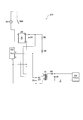
- FIG. 1 is a circuit diagram showing a configuration example of the power supply device according to the first embodiment of the present invention
- FIG. 2 is a circuit diagram for explaining the effects of the present invention.
- a power supply device 100 includes a power supply circuit connected to an AC power supply AC1 for converting alternating current into direct current, and power from the power supply circuit is converted into alternating current to transform a transformer (transformer) T1. And a power supply control circuit for performing control to be supplied to the secondary side.
- a power supply circuit connected to an AC power supply AC1 for converting alternating current into direct current, and power from the power supply circuit is converted into alternating current to transform a transformer (transformer) T1.
- a power supply control circuit for performing control to be supplied to the secondary side.
- the power supply circuit can be composed of, for example, a full-wave rectifier diode D4 (and a smoothing capacitor C4).
- a full-wave rectifier diode D4 for example, a bridge type diode that performs full-wave rectification using a diode bridge can be used.
- the power supply control circuit can be composed of a power supply control circuit IC1 and a power supply start / stop circuit 110, which will be described later, as shown in FIG. Needless to say, the configurations of the power supply circuit and the power supply control circuit are not limited to those illustrated, and may be any configuration as long as they fulfill their functions.
- a control microcomputer (hereinafter referred to as a microcomputer) IC ⁇ b> 2 is taken as an example of a circuit to be supplied with power by the power supply device 100. That is, the microcomputer IC2 is an example of a control unit that controls an electronic device in which the power supply device 100 is incorporated.
- the microcomputer IC ⁇ b> 2 is not supplied with power from the power supply device 100 during standby and is stopped, and performs control to execute the function of the electronic device when power is supplied.
- the power supply device 100 includes a capacitor C3 charged by an AC power supply AC1, a photocoupler PC2 that turns on the power supply control circuit by the power of the capacitor C3, a power start switch SW1, Are provided on the secondary side.
- the photocoupler PC2 turns on the power supply control circuit by the power of the capacitor, and transmits the signal on the secondary side straddling between the primary side and the secondary side in an electrically insulated state to the primary side. It is an example of a switching element.
- the power start switch SW1 is connected between the photocoupler PC2 and the capacitor C3, and is a switch that turns the photocoupler PC2 on by an on operation.
- the power activation switch SW1 is a switch for activating an electronic device (including the microcomputer IC2) incorporating the power supply device 100 from a standby state.
- the photocoupler PC2 is a photocoupler straddling between the primary side and the secondary side.
- the photocoupler PC2 is turned on by turning on the power start switch SW1, and thus the charge charged in the capacitor C3 is turned on.
- the signal is transmitted to the stop circuit 110 as a signal (referred to as an operation start signal).
- a constant voltage diode D3 is connected to the capacitor C3 so that the voltage of the capacitor C3 does not increase too much.
- the power start switch SW1 is on the secondary side, and the control capacity thereof may be determined based on the capacity of the capacitor C3, so that it can be reduced.
- the voltage handled by the power start switch SW1 may be about 5V, so that a normal push switch can be adopted without any problem.
- the power supply start / stop circuit 110 receives the operation start signal from the photocoupler PC2 and transmits a power supply start signal to the power supply control circuit IC1.
- the power supply control circuit IC1 is activated in response to the power activation signal. In this manner, the capacitor C3 is used to operate a circuit (primary side activation circuit) used for activation on the primary side.
- the power supply control circuit IC1 is activated to supply power to the microcomputer IC2 through the transformer T1.
- the power supply device 100 preferably includes another photocoupler PC1.
- This photocoupler PC1 is a photocoupler straddling between the primary side and the secondary side, and is for turning the power supply control circuit off by turning it on.
- the photocoupler PC1 turns the power supply control circuit off by turning it on.
- the photocoupler PC1 is in an electrically insulated state between the primary side and the secondary side, and the secondary side signal is passed to the primary side. It is an example of the other switching element which transmits.
- a signal (referred to as an operation stop signal) is issued from the microcomputer IC2 by pressing a separately provided power stop switch, and the photocoupler PC1 is turned on according to the operation stop signal. That's fine.
- the operation stop signal may be issued from a circuit (not shown) other than the microcomputer IC2, and the photocoupler PC1 may be turned on in accordance with the operation stop signal.
- the power supply start / stop circuit 110 receives the operation stop signal from the photocoupler PC1 and transmits a power supply stop signal to the power supply control circuit IC1. In response to the power stop signal, the power to the power control circuit IC1 is cut off, the power control circuit IC1 is stopped, and the power supply to the microcomputer IC2 through the transformer T1 is stopped. Thus, by providing the photocoupler PC1 for stopping the power supply, the power consumption during the power-off operation can be reduced.
- an internal light emitting element such as a light emitting diode
- an internal light receiving element such as a transistor
- the light receiving element is a transistor, it is turned on.
- the power supply apparatus 100 includes Y capacitors C1 and C2 connected to an AC power supply AC1, and is configured to charge the capacitor C3 with a leakage current of the Y capacitors C1 and C2.
- the Y capacitor is normally used for measures against EMI (Electro-Magnetic Interference), but the power supply device 100 uses the Y capacitors C1 and C2 used for measures against the EMI to charge the capacitor C3.
- EMI Electro-Magnetic Interference
- FIG. 1 an example is shown in which a capacitor C1 and a diode D1 connected in series with the capacitor C2 are frame-connected via a resistor R1, a half-wave rectifier diode D2, and a capacitor C3 to function as a Y capacitor. ing. Thereby, the leakage current from the Y capacitors C1 and C2 is rectified by the half-wave rectifier diode D2, and the capacitor C3 is charged.
- capacitors C1 and C2 constituting the Y capacitor are not limited to this.
- the capacitors C1 and C2 need only have small capacities, and may be ceramic capacitors. However, any capacitors that satisfy the requirements of safety standards may be used.
- the diode D5 will be described in a second embodiment described later.
- the circuit configuration may be such that the capacitor C3 can be indirectly charged from the AC power supply AC1 at the time of standby even if it is not a Y capacitor. Further, the capacitor C3 may be charged from either the primary side or the secondary side.
- the startup time can be shortened compared to the technique described in Patent Document 1 because the startup is performed using the capacitor C3. .
- the power supply start / stop circuit 110 is a circuit that instructs the power supply control circuit IC1 to start and stop according to the signal from the photocoupler PC2 and the signal from the photocoupler PC1 as described above.
- a terminal a is a power supply power input terminal to the power supply start / stop circuit 110.
- Terminals b and c are terminals connected to the photocoupler PC1 and input signals for turning off the power.
- Terminals d and e are terminals connected to the photocoupler PC2 and input signals for turning on the power.
- Terminal f is a power supply terminal to the power supply control circuit IC1.
- the terminal g is a primary ground terminal. In the power supply start / stop circuit 110, the power supply state from the terminal f to the power supply control circuit IC1 is maintained even after the signals from the photocouplers PC2 and PC1 are stopped.
- the terminal h is a power supply power input terminal for inputting power for the power supply control circuit IC1 during operation of the power supply control circuit IC1, and receives power generated by the coil of the transformer T1.
- the power supply control circuit IC1 is an IC that performs power supply control by converting DC power into AC power.
- the terminal m is a power supply terminal (Vcc) of the power supply control circuit IC1
- the terminal j is a primary ground terminal
- the terminal k is a PWM switching terminal.
- the power supply control circuit IC1 switches the voltage rectified by the full-wave rectifier diode D4 by switching the FET (Field effect transistor) in the power supply control circuit IC1 by, for example, PWM (Pulse Width Modulation), thereby switching a predetermined AC pulse. Convert to This predetermined AC pulse is transformed by the transformer T1, and a part thereof is used as a power source for the power supply control circuit IC1, and the other part is used as a power source for the microcomputer IC2.
- the transformer T1 is a transformer with the AC power supply AC1 side as a primary side and the circuit power supply side for the electronic device as a secondary side.
- the AC pulse obtained by switching the voltage obtained by rectifying the AC power supply AC1 by the power supply control circuit IC1 is input to the transformer T1. Further, from the transformer T1, the power supply voltage for the power supply control circuit IC1 is rectified by the half-wave rectifier diode D7 and the smoothing capacitor C6 and output to the terminal h of the power supply start / stop circuit 110. A power supply voltage for moving the microcomputer IC2 of the electronic device is output from the transformer T1. This power supply voltage is rectified by the half-wave rectifier diode D6 and the smoothing capacitor C5 and applied to the microcomputer IC2.
- the power switch SW2 is turned on when starting the power supply circuit.
- a voltage is supplied from the power supply circuit (full-wave rectifier diode D4) to the terminal m (power supply pin Vcc) of the power supply control circuit IC1 through the resistor R9 and the diode D9, and the power supply control circuit IC1 is activated to oscillate the internal PWM.
- the DC power from the full-wave rectifier diode D4 is converted into AC power.
- a voltage is output to each primary winding of the transformer T1, rectified by the half-wave rectifier diode D7 and the smoothing capacitor C6, and then power is stably supplied from the terminal m, so that the power supply control circuit IC1 operates stably. Will do.
- the power supply control circuit IC1 can be activated with the power supplied from the diode D9 side, but such a circuit is used because the stable operation of the power supply control circuit IC1 cannot be continued. Since the voltage rectified by the half-wave rectifier diode D6 and the smoothing capacitor C5 is output through the transformer T1 by the stable operation of the power supply control circuit IC1, the microcomputer IC2 can be operated stably.
- the power supply device 200 since the power switch SW2 is connected to the AC power supply AC1 on the primary side, it is necessary to increase the control capacity. That is, the power supply device 200 requires an AC switch having a large control capacity in order to completely turn off the power supply circuit (full-wave rectifier diode D4).
- the power supply start switch SW1 when starting the power supply circuit, the power supply start switch SW1 is turned on to use the small-capacity electric power charged in the capacitor C3 to make the photocoupler PC2 Turns on. Thereby, a voltage is supplied to the terminal m of the power supply control circuit IC1, and similarly, the power supply control circuit IC1 can be stably operated, and the microcomputer IC2 can be stably operated.
- the photocoupler PC1 is turned on from the microcomputer IC2. As a result, no voltage is supplied to the terminal m of the power supply control circuit IC1, so that the operation of the power supply control circuit IC1 can be stopped.
- the power supply device 100 since the power supply is activated by the small-capacity power charged in the secondary side capacitor C3, it is not necessary to provide a power switch with a large control capacity unlike the power supply device 200. Since it is activated by the photocoupler, the space occupied on the substrate can be reduced, and the circuit arrangement on the substrate is flexible and easy. Furthermore, in the power supply apparatus 100, it is not necessary to cut off the power supply to the primary circuit of the power supply circuit with a power switch as provided in the power supply apparatus 200. It can be as short as possible.
- the power supply control circuit IC1 stops operating during standby, power consumption during standby is basically only consumed by the primary side startup circuit, and standby power can be kept very low. it can. That is, the power loss during standby of the power supply apparatus 100 is basically only the loss of the primary side startup circuit, which is advantageous in terms of standby power. This effect basically does not depend on whether or not the photocoupler PC1 is provided.
- the primary side startup circuit can be configured with a small number of parts, which is advantageous in terms of cost.
- the standby power can be kept low while shortening the startup time.
- the primary-side power supply control circuit IC1 is activated by the power transmitted to the secondary-side capacitor C3 due to the leakage current from the Y capacitors C1 and C2. It becomes possible to take EMI countermeasures while keeping the values within the values stipulated in the safety standards. Even when the Y capacitors C1 and C2 are provided, the power loss during standby of the power supply device 100 is only the transmission loss of the Y capacitors C1 and C2 and the loss of the primary side startup circuit, so the standby power is very low. Can be suppressed.
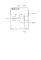
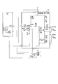
- FIGS. 3 is a circuit diagram showing a configuration example mainly of the power supply start / stop circuit in the power supply device of FIG. 1, and FIG. 4 shows a detailed configuration example of the power supply start / stop circuit in the power supply device of FIG. It is a circuit diagram which shows the internal structural example of a power supply control circuit.
- the power supply start / stop circuit 110 is provided with a diode 111, a diode 112, a switch element 113, and a regulator (REG) 114.
- the switch element 113 is opened in response to an operation stop signal from the photocoupler PC1, and is closed in response to an operation start signal from the photocoupler PC2.
- the REG 114 is a circuit that is connected to the switch element 113 and keeps the power supply voltage output to the power supply control circuit IC1 constant.
- the power to the power supply control circuit IC1 is either supplied from the full-wave rectifier diode D4 via the diode 111 or supplied from the transformer T1 via the diode 112. Then, when the photocoupler PC2 and the photocoupler PC1 are turned on, the power supply to the power supply control circuit IC1 is turned on and off by the switch element 113, respectively.
- ON / OFF by the switch element 113 is configured to be held even after the signals from the photocouplers PC2 and PC1 are stopped.
- the power supply voltage becomes a constant voltage suitable for the power supply control circuit IC1 by the REG 114 and is supplied to the power supply control circuit IC1.
- FIG. 4 includes a resistor R3 to R10, diodes D8 to D10, a capacitor C7, a constant voltage diode Z1, and transistors pnp1, npn2, and npn3.
- the type of the transistor is indicated by a symbol.
- FIG. 4 the resistance value, voltage value, capacitance, and the like of each element are illustrated, but this is merely an example, and the present invention is not limited to this.
- the wiring between specific elements is as shown in FIG. 4 and will not be described.
- the states of the three transistor transistors pnp1, npn2, and npn3 are determined by the signals from the photocouplers PC2 and PC1. The structure is maintained even after stopping, and operates as follows when the power supply control circuit IC1 is started / stopped.
- the transistors pnp1 and npn2 are in an on state and the transistor npn3 is in an off state, as will be described later in a stopped state.
- the transistor npn2 is turned off in the power start / stop circuit 110.
- the transistor pnp1 is turned off and the transistor npn3 is turned on.
- the transistor npn3 When the transistor npn3 is turned on, a voltage is supplied to the terminal m of the power supply control circuit IC1, the power supply control circuit IC1 is activated, the internal PWM starts oscillating, and the power supply control circuit IC1 is stably operated. be able to.
- the transistors pnp1 and npn2 are in the off state and the transistor npn3 is in the on state as the activated state.
- the photocoupler PC1 is temporarily turned on by transmitting an operation stop signal (on pulse for a predetermined time) from the microcomputer IC2 in such a start state (power supply state)
- the power supply start / stop circuit 110 Since the transistor npn2 is turned on and the transistor pnp1 is turned on, the transistor npn3 is turned off. Since the transistor npn3 is turned off, no voltage is supplied to the terminal m of the power supply control circuit IC1, so that the operation of the power supply control circuit IC1 can be stopped.
- the television apparatus includes a display unit, a speaker unit, a tuner unit, and the like, and displays a video indicated by the video signal on the display unit among broadcast signals received by the tuner unit, and outputs audio indicated by the audio signal from the speaker unit. It is configured as follows. Note that when the display unit includes a non-self-luminous display panel such as a liquid crystal panel, the display unit also includes a backlight device.
- the television apparatus includes the power supply apparatus 100 of FIG. 1 described above, and is provided with a microcomputer IC2 as a control unit.
- This television apparatus is configured such that power is supplied from, for example, the power supply circuit of the power supply apparatus 100 in a state in which the microcomputer IC2 is operating to parts that require power supply, such as a display unit, a speaker unit, and a tuner unit. Just keep it.
- the capacitor C3 in the example of FIG. 1 is charged with the leakage current from the primary side during standby, as described in the first embodiment, but after starting up the electronic device, the capacitor C3 is connected from the transformer T1 via the diode D5. It is configured to be charged by the supplied power.
- the diode D5 is provided to assist charging of the capacitor C3 from the Y capacitors C1 and C2.
- a configuration in which the diode D5 is not provided is also conceivable.
- the diode D5 is not provided, charging from the Y capacitors C1 and C2 takes time. Therefore, when the capacitor C3 is not sufficiently charged, the power start switch SW1 is set. Even if the power is turned on, the power supply cannot be restarted, and it is necessary to wait until the capacitor C3 is charged with the leakage current.
- the AC power supply AC1 is connected to the power supply apparatus 100 to start the power supply apparatus 100, and the photocoupler PC1 is turned on immediately after the start-up to stop the power supply. It can happen in a scene.
- the capacitor C3 is immediately charged with the charge supplied from the half-wave rectifier diode D6 and the smoothing capacitor C5 even when restarting in a short time.
- the power can be restarted by the power start switch SW1.
- the power supply device includes a power supply circuit that is connected to an AC power supply and converts alternating current to direct current, and a control that converts the power from the power supply circuit into alternating current and supplies it to the secondary side via a transformer.
- a power supply device comprising: a capacitor charged by the AC power supply; a primary side for turning on the power supply control circuit by the power of the capacitor; and the secondary Between the switching element and the capacitor, the switching element transmitting the secondary side signal to the primary side in an electrically insulated state between the switching element and the capacitor.
- a power start switch that is turned on is provided on the secondary side.
- the start-up time is avoided without using a power switch with a large control capacity and without costing an additional circuit.
- the standby power can be kept low while shortening.
- the power supply device further includes a Y capacitor connected to the AC power supply, and the capacitor is charged by a leakage current of the Y capacitor.
- the leakage current can be used for charging the capacitor while taking measures against EMI.
- DESCRIPTION OF SYMBOLS 100 Power supply device, 110 ... Power supply start / stop circuit, 111, 112 ... Diode, 113 ... Switch element, 114 ... REG, AC1 ... AC power supply, C1, C2 ... Y capacitor, C3 ... Capacitor, C4, C5, C6 ... Smoothing capacitors, D1, D2, D5, D6, D7 ... diode, D3 ... constant voltage diode, D4 ... full-wave rectifier diode, IC1 ... power supply control circuit, IC2 ... microcomputer, PC1, PC2 ... photocoupler, R1 ... resistor, SW1 ... Power start switch, T1 ... Transformer.
Landscapes
- Engineering & Computer Science (AREA)
- Power Engineering (AREA)
- Rectifiers (AREA)
- Stand-By Power Supply Arrangements (AREA)
- Direct Current Feeding And Distribution (AREA)
- Dc-Dc Converters (AREA)
Abstract
電源回路からの電力を交流変換してトランスを介して2次側に供給する電源装置において、大きな制御容量の電源スイッチを使用せず追加の回路にコストをかけずに、起動時間を短縮しつつ待機電力を低く抑える。電源装置(100)は、交流電源に接続され交流を直流に変換する電源回路と、その電源回路からの電力を交流変換しトランス(T1)を介して2次側に供給する制御を行う電源供給制御回路と、を備える。電源装置(100)は、上記交流電源により充電されるコンデンサ(C3)と、コンデンサ(C3)の電力により上記電源供給制御回路をオン状態にする、1次側と2次側との間に電気的に絶縁状態でまたがり上記2次側の信号を上記1次側に伝達するスイッチング素子と、上記スイッチング素子とコンデンサ(C3)との間に接続され、オン操作により上記スイッチング素子をオン状態にする電源起動スイッチ(SW1)と、を2次側に備える。
Description
本発明は、電源装置、テレビ装置、及び電子機器に関し、より詳細には、電源回路からの電力を交流変換してトランスを介して2次側に供給する電源装置、並びにその電源装置を備えた電子機器及びテレビ装置に関する。
従来から、電気機器の待機時電力を削減するための方法として、待機専用コンバータを設ける方法や、或いは待機時に間欠発振モードになる電源IC(Integrated Circuit)等を設ける方法が採用されている。
しかしながら、これらの方法による電力削減には限界があり、待機電力を限りなく0ワットに近づけることが困難であった。また、待機電力を0ワット相当とするために、複雑な回路構成を採用することも考えられるが、コストが嵩んでしまう。
この課題を解決する技術として、特許文献1には、トランスを介した2次側の主回路に接続され且つバックアップ電力が必要な補助回路に対してバックアップ電力を供給する補助電源回路を設けた電源回路において、その補助電源回路には認定コンデンサを使用してバックアップ電力を供給する技術が開示されている。
また、従来の電源回路には、トランスの2次側に大容量コンデンサを設け、その大容量コンデンサに充電された電力により、1次側の電源を起動させる方式を採用したものもある。
しかしながら、特許文献1に記載の技術では、電子機器内の情報をバックアップするための補助回路を常に動作させる必要があり、補助回路のための所定の電力が必要である。そのため、2次側に電力を供給するために大容量の認定コンデンサを使用する必要がある。しかし、1次側から2次側に漏洩する電流(漏洩電流)がコンデンサの容量と入力電圧の大きさに比例して増加することから、コンデンサの容量が大きすぎると、機器の安全規格で定められた漏洩電流値を超えてしまう。そのため、この技術では、その漏洩電流値を超えない程度の大容量のコンデンサを使用することしかできず、充分なバックアップ電力を供給することができなくなる。
また、この技術は、AC電源に接続された電源スイッチがオフとなった場合において2次側に電力を供給するためのものであり、電源スイッチがオフの場合には、電源装置の1次側回路には通電がなく、電源スイッチをオンにしてから電源起動(2次側出力の立上り)までに時間がかかる課題がある。さらに、この電源スイッチは、安全規格認可品を使用する必要があり、コストが高く、構造上基板上に占有するスペースが大きく、且つ基板上での配置に配慮が必要となる。
また、2次側の大容量コンデンサの電力で1次側の電源を起動させる技術では、コスト高のコンデンサを使用しなければならず、常時充電を行うための電源回路が必要となり、待機電力、コスト的には有利とは言えない。
本発明は、上述のような実状に鑑みてなされたものであり、その目的は、電源回路からの電力を交流変換してトランスを介して2次側に供給する電源装置において、大きな制御容量の電源スイッチを使用せず且つ追加の回路にコストをかけずに、起動時間を短縮しつつ待機電力を低く抑えること、並びにそのような電源装置を備えた電子機器、テレビ装置を提供することにある。
上記の課題を解決するために、本発明の第1の技術手段は、交流電源に接続され交流を直流に変換する電源回路と、該電源回路からの電力を交流変換しトランスを介して2次側に供給する制御を行う電源供給制御回路と、を備えた電源装置であって、前記交流電源により充電されるコンデンサと、該コンデンサの電力によって前記電源供給制御回路をオン状態にする、1次側と前記2次側との間に電気的に絶縁状態でまたがり前記2次側の信号を該1次側に伝達するスイッチング素子と、該スイッチング素子と前記コンデンサとの間に接続され、オン操作により前記スイッチング素子をオン状態にする電源起動スイッチと、を前記2次側に備えたことを特徴としたものである。
本発明の第2の技術手段は、第1の技術手段において、前記交流電源に接続されたYコンデンサをさらに備え、該Yコンデンサの漏れ電流により前記コンデンサを充電することを特徴としたものである。
本発明の第3の技術手段は、第1又は第2の技術手段において、オン状態にすることで、前記電源供給制御回路をオフ状態にする他のスイッチング素子をさらに備え、該他のスイッチング素子は前記1次側と前記2次側との間に電気的に絶縁状態でまたがり前記2次側の信号を前記1次側に伝達する素子であることを特徴としたものである。
本発明の第4の技術手段は、第1~第3のいずれか1の技術手段における電源装置を備えた電子機器である。
本発明の第5の技術手段は、第1~第3のいずれか1の技術手段における電源装置を備えたテレビ装置である。
本発明の第5の技術手段は、第1~第3のいずれか1の技術手段における電源装置を備えたテレビ装置である。
本発明によれば、電源回路からの電力を交流変換してトランスを介して2次側に供給する電源装置において、大きな制御容量の電源スイッチを使用せず且つ追加の回路にコストをかけずに、起動時間を短縮しつつ待機電力を低く抑えることができる。また、本発明によれば、そのような電源装置を備えた電子機器やテレビ装置を提供することができる。
以下、本発明に係る電源装置の様々な実施形態について、図面を参照しながら説明する。この電源装置は、待機時から起動するための回路に特徴を有するものであり、テレビ装置、レコーダ機器など様々な電子機器に組み込むことが可能である。
(第1の実施形態)
本発明の第1の実施形態に係る電源装置について、図1及び図2を参照しながら説明する。図1は、本発明の第1の実施形態に係る電源装置の一構成例を示す回路図で、図2は、本発明による効果を説明するための回路図である。
本発明の第1の実施形態に係る電源装置について、図1及び図2を参照しながら説明する。図1は、本発明の第1の実施形態に係る電源装置の一構成例を示す回路図で、図2は、本発明による効果を説明するための回路図である。
図1に示すように、本実施形態に係る電源装置100は、交流電源AC1に接続され交流を直流に変換する電源回路と、その電源回路からの電力を交流変換しトランス(変圧器)T1を介して2次側に供給する制御を行う電源供給制御回路と、を備えている。
交流電源AC1としては、例えば100V等の商用電源が挙げられる。上記電源回路は、図1で示すように、例えば全波整流ダイオードD4(及び平滑コンデンサC4)で構成することができる。全波整流ダイオードD4としては、例えばダイオードブリッジによる全波整流を行うブリッジ形のものが挙げられる。
上記電源供給制御回路は、図1で示すように、後述する電源制御回路IC1及び電源起動・停止回路110で構成することができる。無論、上記電源回路や上記電源供給制御回路の構成は例示するものに限ったものではなく、それらの機能を果たす構成であればよい。
また、図1では、電源装置100で電力を供給する対象となる回路の一例として制御用のマイクロコンピュータ(以下、マイコンと言う)IC2を、例に挙げている。つまり、マイコンIC2は、電源装置100を組み込む電子機器を制御する制御部の一例である。マイコンIC2は、待機時には電源装置100からの電力が供給されておらず停止しており、電力供給時にその電子機器が有する機能を実行させる制御を行う。
そして、本発明の主たる特徴として、電源装置100は、交流電源AC1により充電されるコンデンサC3と、コンデンサC3の電力によって上記電源供給制御回路をオン状態にするフォトカプラPC2と、電源起動スイッチSW1と、を2次側に備えている。フォトカプラPC2は、コンデンサの電力によって上記電源供給制御回路をオン状態にする、1次側と2次側との間に電気的に絶縁状態でまたがり2次側の信号を1次側に伝達するスイッチング素子の一例である。
電源起動スイッチSW1は、フォトカプラPC2とコンデンサC3との間に接続され、オン操作によりフォトカプラPC2をオン状態にするスイッチである。電源起動スイッチSW1は、待機状態からこの電源装置100を組み込んだ電子機器(マイコンIC2を含む)を起動するためのスイッチである。
フォトカプラPC2は、1次側と2次側との間にまたがるフォトカプラであり、電源起動スイッチSW1をオン操作することでオン状態になり、これによりコンデンサC3に充電された電荷は電源起動・停止回路110に信号(動作起動信号と呼ぶ)として伝送される。図1の例では、コンデンサC3に定電圧ダイオードD3が接続され、コンデンサC3の電圧が上昇し過ぎないようになっている。
フォトカプラPC2をオン状態にし電源起動・停止回路110を動作させるためには、その定格にもよるが、例えば1~5mA程度の電流を100nsec程度以上の時間流すことが必要であり、コンデンサC3の容量やオン操作と認識する時間はそれによって決定しておけばよい。
また、電源起動スイッチSW1は2次側にあり、その制御容量はコンデンサC3の容量に基づいて決定すればよいため、小さくできる。例えば、電源起動スイッチSW1で扱う電圧は5V程度で済み、そのため、通常のプッシュスイッチを問題なく採用できる。
電源起動・停止回路110は、このフォトカプラPC2からの動作起動信号を受けて、電源制御回路IC1に電源起動信号を送信する。電源制御回路IC1は、上記電源起動信号を受けて起動する。このように、コンデンサC3は、1次側において起動に用いる回路(1次側の起動回路)を動作させるために用いられる。そして、電源制御回路IC1は、起動することで、トランスT1を介してマイコンIC2に電力を供給する。
また、電源装置100は、他のフォトカプラPC1を備えることが好ましい。このフォトカプラPC1は、1次側と2次側との間にまたがるフォトカプラであり、オン状態にすることで、上記電源供給制御回路をオフ状態にするためのものである。フォトカプラPC1は、オン状態にすることで上記電源供給制御回路をオフ状態にする、1次側と2次側との間に電気的に絶縁状態でまたがり2次側の信号を1次側に伝達する他のスイッチング素子の一例である。フォトカプラPC1をオン状態にする際には、例えば別途設けた電源停止スイッチの押下操作によりマイコンIC2から信号(動作停止信号と呼ぶ)を発し、その動作停止信号に従ってフォトカプラPC1をオン状態にすればよい。無論、動作停止信号は、マイコンIC2以外の回路(図示せず)から発し、その動作停止信号に従ってフォトカプラPC1をオン状態にしてもよい。
電源起動・停止回路110は、このフォトカプラPC1からの動作停止信号を受けて、電源制御回路IC1に電源停止信号を送信する。上記電源停止信号を受けて、電源制御回路IC1への電力が遮断され、電源制御回路IC1が停止し、トランスT1を介したマイコンIC2への電力供給が停止される。このように、電源停止のためにフォトカプラPC1を設けることにより、電源オフ操作時の消費電力を低減することができる。
また、フォトカプラPC1,PC2はいずれも、内部の発光素子(発光ダイオード等)が2次側からの電気信号を光に変換し、内部の受光素子(トランジスタ等)がその光を受けて電気信号に変換して出力する。受光素子がトランジスタの場合、それがオン状態になる。このように、フォトカプラPC1,PC2はいずれも光により制御されるため、1次側と2次側を絶縁することができる。
以下、電源装置100の詳細について説明する。
まず、電源装置100におけるコンデンサC3への充電方法について説明する。電源装置100は、交流電源AC1に接続されたYコンデンサC1,C2を備え、YコンデンサC1,C2の漏れ(リーク)電流によりコンデンサC3を充電するように構成されている。Yコンデンサは、通常、EMI(Electro-Magnetic Interference)対策に用いられるが、電源装置100では、そのEMI対策に用いたYコンデンサC1,C2を利用して、コンデンサC3を充電するようにしている。
まず、電源装置100におけるコンデンサC3への充電方法について説明する。電源装置100は、交流電源AC1に接続されたYコンデンサC1,C2を備え、YコンデンサC1,C2の漏れ(リーク)電流によりコンデンサC3を充電するように構成されている。Yコンデンサは、通常、EMI(Electro-Magnetic Interference)対策に用いられるが、電源装置100では、そのEMI対策に用いたYコンデンサC1,C2を利用して、コンデンサC3を充電するようにしている。
図1では、コンデンサC1とコンデンサC2に直列されたダイオードD1との間を、抵抗R1、半波整流ダイオードD2、及びコンデンサC3を介してフレーム接続することで、Yコンデンサとして機能させた例を挙げている。これにより、YコンデンサC1,C2からの漏れ電流を半波整流ダイオードD2で整流し、コンデンサC3に充電している。
なお、Yコンデンサを構成するコンデンサC1とコンデンサC2との間のフレーム接続又は接地の例はこれに限ったものではない。また、コンデンサC1,C2は少容量で足りるためセラミックコンデンサを用いればよいが、安全規格上要求される条件を満たす認定コンデンサであればよい。なお、ダイオードD5については、後述する第2の実施形態で説明する。
また、YコンデンサC1,C2を設けた例を挙げているが、Yコンデンサでなくても、待機時において交流電源AC1から間接的にコンデンサC3を充電できるような回路構成になっていればよい。また、コンデンサC3への充電は、1次側、2次側のどちら側から行うような構成であってもよい。無論、YコンデンサC1,C2を設けない構成であっても、コンデンサC3を用いて起動することに変わりはないため、特許文献1に記載の技術に比べて起動時間を短縮することができると言える。
次に、電源起動・停止回路110及び電源制御回路IC1について説明する。
電源起動・停止回路110は、上述のようにフォトカプラPC2からの信号、フォトカプラPC1からの信号に応じて、それぞれ電源制御回路IC1にそれぞれ起動、停止を指示する回路である。端子aは、電源起動・停止回路110への電源電力入力端子である。端子b,cは、フォトカプラPC1に接続された端子であり、電源をオフするための信号の入力端子である。端子d,eは、フォトカプラPC2に接続された端子であり、電源をオンするための信号の入力端子である。
電源起動・停止回路110は、上述のようにフォトカプラPC2からの信号、フォトカプラPC1からの信号に応じて、それぞれ電源制御回路IC1にそれぞれ起動、停止を指示する回路である。端子aは、電源起動・停止回路110への電源電力入力端子である。端子b,cは、フォトカプラPC1に接続された端子であり、電源をオフするための信号の入力端子である。端子d,eは、フォトカプラPC2に接続された端子であり、電源をオンするための信号の入力端子である。
端子fは、電源制御回路IC1への電力供給端子である。端子gは、1次側グランド用の端子である。電源起動・停止回路110では、端子fからの電源制御回路IC1への電力供給状態がフォトカプラPC2,PC1からの信号が停止した後も保持される構造となっている。端子hは、電源制御回路IC1の動作時に電源制御回路IC1用の電力を入力するための電源電力入力端子であり、トランスT1のコイルで生成された電力が入力される。
電源制御回路IC1は、直流電力を交流電力に変換して電源制御を行うICである。端子mは電源制御回路IC1の電源端子(Vcc)、端子jは1次側グランド用の端子、端子kはPWMスイッチング端子である。電源制御回路IC1は、例えばPWM(Pulse Width Modulation)により電源制御回路IC1内のFET(Field effect transistor)をスイッチングすることで、全波整流ダイオードD4で整流された電圧をスイッチングして所定の交流パルスに変換する。この所定の交流パルスは、トランスT1によって変圧などがなされ、一部は電源制御回路IC1の電源となり、他の一部はマイコンIC2の電源として使用される。
このような交流パルスのトランスT1への入力及びマイコンIC2への電圧印加について説明する。トランスT1は、交流電源AC1側を1次側、上記電子機器用の回路電源側を2次側とする変圧トランスである。
トランスT1には、交流電源AC1を整流した電圧について電源制御回路IC1でスイッチングして得た上記交流パルスが入力される。また、トランスT1からは、電源制御回路IC1用の電源電圧が半波整流ダイオードD7及び平滑コンデンサC6により整流されて、電源起動・停止回路110の端子hに出力される。また、トランスT1からは、上記電子機器のマイコンIC2を動かすための電源電圧が出力される。この電源電圧は、半波整流ダイオードD6及び平滑コンデンサC5で整流されて、マイコンIC2に印加される。
次に、図2を参照しながら、本発明による効果について説明する。まず、本発明の主たる特徴であるコンデンサC3、フォトカプラPC2、及び電源起動スイッチSW1を有する回路(以下、本回路と呼ぶ)が無い場合について説明する。本回路が具備されていない場合、図2に示す電源装置200のような回路構成となり、交流電源AC1に電源スイッチSW2を接続することになる。なお、図2において、抵抗R9及びダイオードD9は、後述する図4の回路構成例に合わせて設けている。
電源装置200では、電源回路を起動する際、電源スイッチSW2をオンにする。それにより、抵抗R9及びダイオードD9を通じて電源制御回路IC1の端子m(電源pin Vcc)に電源回路(全波整流ダイオードD4)から電圧が供給され、電源制御回路IC1が起動して内部のPWMが発振を開始し、全波整流ダイオードD4からの直流電力を交流電力に変換する。
それによってトランスT1の1次側の各巻線に電圧が出力され、半波整流ダイオードD7及び平滑コンデンサC6で整流された後、端子mから電力が安定供給され、電源制御回路IC1が安定して動作することになる。なお、ダイオードD9側から供給される電力では電源制御回路IC1を起動できるが、電源制御回路IC1の安定動作を継続できないため、このような回路を用いている。そして、電源制御回路IC1の安定した動作により、トランスT1を介して半波整流ダイオードD6と平滑コンデンサC5で整流された電圧が出力されるため、マイコンIC2を安定して動作させることができる。
しかしながら、電源装置200では、電源スイッチSW2が1次側の交流電源AC1に接続されているため、制御容量を大きくする必要がある。つまり、電源装置200では、電源回路(全波整流ダイオードD4)を完全にオフさせるために、制御容量の大きなACスイッチを必要とする。
一方、本回路が具備された電源装置100では、電源回路を起動させる際には、電源起動スイッチSW1をオン操作することで、コンデンサC3に充電された小容量の電力を利用してフォトカプラPC2がオン状態になる。これにより、電源制御回路IC1の端子mに電圧が供給されて、同様に、電源制御回路IC1を安定して動作させ、マイコンIC2も安定して動作させることができる。
また、電源装置100では、電源回路を完全にオフさせる際、マイコンIC2からフォトカプラPC1をオン状態にする。これにより、電源制御回路IC1の端子mに電圧が供給されなくなるため、電源制御回路IC1の動作を停止させることができる。
このように、電源装置100では、2次側のコンデンサC3に充電された小容量の電力により電源起動を行うため、電源装置200のように制御容量の大きな電源スイッチを設ける必要がなく、代わりにフォトカプラにより起動させるため、基板上占有するスペースを小さくでき、基板上の回路配置にも自由度があり、容易になる。さらに、電源装置100では、電源装置200に設けたような電源スイッチで電源回路の1次側回路への電力供給を遮断する必要がないため、電源装置200に比べてスイッチオン時の起動時間を極力短くすることができる。
また、電源装置100では、待機時には電源制御回路IC1が動作を停止しているため、待機時の電力消費は基本的に1次側起動回路での消費だけとなり、待機電力も大変低く抑えることができる。つまり、電源装置100の待機時の電力損失は、基本的に1次側起動回路の損失分のみとなるため、待機電力的に有利となる。なお、この効果は、基本的にフォトカプラPC1を具備するか否かに依らない。その他、電源装置100では、図1の例からも分かるように、少ない部品点数で1次側の起動回路が構成でき、コスト的に有利になる。
このように、本発明によれば、電源回路からの電力を交流変換してトランスを介して2次側に供給するに際し、大きな制御容量の電源スイッチを使用せず且つ追加の回路にコストをかけずに、起動時間を短縮しつつ待機電力を低く抑えることができる。
また、YコンデンサC1,C2を設けた場合には、そのYコンデンサC1,C2からの漏れ電流によって2次側のコンデンサC3に伝達された電力で1次側の電源制御回路IC1を起動させるため、容易に安全規格で規定された数値内に抑えつつEMI対策も施すことができるようになる。また、YコンデンサC1,C2を設けた場合でも、電源装置100の待機時の電力損失はYコンデンサC1,C2の伝送ロスと1次側起動回路の損失分のみとなるため、待機電力を大変低く抑えることができる。
次に、図1の電源装置100に設ける電源起動・停止回路110の具体例について、図3及び図4を参照しながら説明する。図3は、図1の電源装置における主に電源起動・停止回路の部分の一構成例を示す回路図で、図4は、図1の電源装置における電源起動・停止回路の詳細な構成例及び電源制御回路の内部構成例を示す回路図である。
図3に示すように、電源起動・停止回路110には、ダイオード111、ダイオード112、スイッチ素子113、及びレギュレータ(REG)114が設けられている。スイッチ素子113は、フォトカプラPC1からの動作停止信号を受けて開かれ、フォトカプラPC2からの動作起動信号を受けて閉じられる。REG114は、スイッチ素子113に接続されると共に、電源制御回路IC1に出力する電源電圧を一定に保つ回路である。
電源制御回路IC1への電力は、全波整流ダイオードD4からダイオード111を介して供給されるか、若しくはトランスT1からダイオード112を介して供給されるかのいずれかとなっている。そして、フォトカプラPC2、フォトカプラPC1がオン状態になることによって、スイッチ素子113により電源制御回路IC1への電力供給がそれぞれオン、オフされる。ここで、スイッチ素子113によるオン、オフは、フォトカプラPC2,PC1からの信号が停止した後も保持される構造となっている。オン時には、REG114によって電源電圧は、電源制御回路IC1に適した一定の電圧となり、電源制御回路IC1に供給される。
図4で例示する電源起動・停止回路110は、抵抗R3~R10、ダイオードD8~D10、コンデンサC7、定電圧ダイオードZ1、及びトランジスタpnp1,npn2,npn3を有する。ここで、トランジスタの型は記号で示している。なお、図4では、各素子の抵抗値、電圧値、静電容量などを図示しているが、単なる一例に過ぎず、これに限ったものではない。
この電源起動・停止回路110は、具体的な素子間の配線については図4の通りであり説明しないが、3つのトランジスタトランジスタpnp1,npn2,npn3の状態は、フォトカプラPC2,PC1からの信号が停止した後も保持される構造となっており、電源制御回路IC1の起動/停止の際に、以下のように動作する。
まず、電源制御回路IC1を起動させる際について説明する。起動させる前は、停止させた状態として後述するように、トランジスタpnp1,npn2がオン状態、トランジスタnpn3がオフ状態となっている。そのような待機状態で、電源起動スイッチSW1がオン操作され所定時間オンのパルスが出力されることでフォトカプラPC2が一時的にオン状態になると、電源起動・停止回路110では、トランジスタnpn2がオフ状態となるため、トランジスタpnp1がオフ状態になり、トランジスタnpn3がオン状態になる。トランジスタnpn3がオン状態になることで、電源制御回路IC1の端子mに電圧が供給され、電源制御回路IC1が起動して内部のPWMが発振を開始し、電源制御回路IC1を安定して動作させることができる。
次に、電源制御回路IC1を完全に停止させる際について説明する。停止させる前は、起動させた状態として上述したように、トランジスタpnp1,npn2がオフ状態、トランジスタnpn3がオン状態となっている。そのような起動状態(電力供給状態)で、マイコンIC2から動作停止信号(所定時間オンのパルス)を伝送することでフォトカプラPC1が一時的にオン状態になると、電源起動・停止回路110では、トランジスタnpn2がオン状態になり、トランジスタpnp1がオン状態になるため、トランジスタnpn3がオフ状態となる。トランジスタnpn3がオフ状態になることで、電源制御回路IC1の端子mに電圧が供給されなくなるため、電源制御回路IC1の動作を停止させることができる。
次に、上述したような電源装置を備えたテレビ装置やその他の電子機器について簡単に説明する。ここでは、テレビ装置の一構成例について説明する。テレビ装置は、表示部、スピーカ部、チューナ部等を備え、チューナ部で受信した放送信号のうち、映像信号が示す映像をその表示部に表示させ、音声信号が示す音声をスピーカ部から出力するように構成されている。なお、表示部は、液晶パネルのように非自発光型の表示パネルを有する場合、バックライト装置も有することになる。そして、このテレビ装置には、上述した図1の電源装置100を備え、制御部としてのマイコンIC2が設けられている。このテレビ装置では、表示部、スピーカ部、チューナ部などの電源供給が必要な部位に対し、マイコンIC2が稼働した状態で電源装置100の例えば上記電源回路から電源が供給されるように構成しておけばよい。
(第2の実施形態)
本発明の第2の実施形態として、ダイオードD5によってコンデンサC3を充電する例について説明する。
本発明の第2の実施形態として、ダイオードD5によってコンデンサC3を充電する例について説明する。
図1の例におけるコンデンサC3は、待機時には第1の実施形態で説明したようにして1次側からの漏れ電流で充電されるが、電子機器の起動後は、ダイオードD5を介してトランスT1から供給される電力によって充電されるように構成されている。
ダイオードD5は、YコンデンサC1,C2からのコンデンサC3への充電を補助するために設けられている。無論、ダイオードD5を設けない構成も考えられるが、ダイオードD5が無い場合、YコンデンサC1,C2からの充電は時間がかかるため、コンデンサC3が充分に充電されていない状態では、電源起動スイッチSW1をオン操作しても電源を再起動できず、コンデンサC3が漏れ電流で充電されるまで待たなければならない。コンデンサC3が充分に充電されていない状態は、例えば、この電源装置100に交流電源AC1を接続して電源装置100を起動させ、且つ起動直後にフォトカプラPC1をオン状態にして電源を停止させた場面で起こり得る。
それに対し、ダイオードD5を設けることで、半波整流ダイオードD6及び平滑コンデンサC5から供給される電荷で、短時間での再起動時においても直ぐにコンデンサC3が充電されるため、このような場面でも直ぐに電源起動スイッチSW1での電源再起動が可能となる。
但し、このような場面を除けば、喩えダイオードD5を設けない構成であっても、特許文献1に記載の技術のように電源スイッチを入れてから2次側の立上りまでに時間がかかることはないため、起動時間を短縮することは可能である。
(第1、第2の実施形態について)
以上説明したように、本発明に係る電源装置は、交流電源に接続され交流を直流に変換する電源回路と、上記電源回路からの電力を交流変換しトランスを介して2次側に供給する制御を行う電源供給制御回路と、を備えた電源装置であって、上記交流電源により充電されるコンデンサと、上記コンデンサの電力によって上記電源供給制御回路をオン状態にする、1次側と上記2次側との間に電気的に絶縁状態でまたがり上記2次側の信号を上記1次側に伝達するスイッチング素子と、上記スイッチング素子と上記コンデンサとの間に接続され、オン操作により上記スイッチング素子をオン状態にする電源起動スイッチと、を上記2次側に備えたことを特徴としたものである。これにより、電源回路からの電力を交流変換してトランスを介して2次側に供給する電源装置において、大きな制御容量の電源スイッチを使用せず且つ追加の回路にコストをかけずに、起動時間を短縮しつつ待機電力を低く抑えることができる。
以上説明したように、本発明に係る電源装置は、交流電源に接続され交流を直流に変換する電源回路と、上記電源回路からの電力を交流変換しトランスを介して2次側に供給する制御を行う電源供給制御回路と、を備えた電源装置であって、上記交流電源により充電されるコンデンサと、上記コンデンサの電力によって上記電源供給制御回路をオン状態にする、1次側と上記2次側との間に電気的に絶縁状態でまたがり上記2次側の信号を上記1次側に伝達するスイッチング素子と、上記スイッチング素子と上記コンデンサとの間に接続され、オン操作により上記スイッチング素子をオン状態にする電源起動スイッチと、を上記2次側に備えたことを特徴としたものである。これにより、電源回路からの電力を交流変換してトランスを介して2次側に供給する電源装置において、大きな制御容量の電源スイッチを使用せず且つ追加の回路にコストをかけずに、起動時間を短縮しつつ待機電力を低く抑えることができる。
また、上記電源装置は、上記交流電源に接続されたYコンデンサをさらに備え、上記Yコンデンサの漏れ電流により上記コンデンサを充電することが好ましい。これにより、EMI対策を施しつつ、その漏れ電流を上記コンデンサの充電に利用することができる。
100…電源装置、110…電源起動・停止回路、111,112…ダイオード、113…スイッチ素子、114…REG、AC1…交流電源、C1,C2…Yコンデンサ、C3…コンデンサ、C4,C5,C6…平滑コンデンサ、D1,D2,D5,D6,D7…ダイオード、D3…定電圧ダイオード、D4…全波整流ダイオード、IC1…電源制御回路、IC2…マイコン、PC1,PC2…フォトカプラ、R1…抵抗、SW1…電源起動スイッチ、T1…トランス。
Claims (5)
- 交流電源に接続され交流を直流に変換する電源回路と、該電源回路からの電力を交流変換しトランスを介して2次側に供給する制御を行う電源供給制御回路と、を備えた電源装置であって、
前記交流電源により充電されるコンデンサと、該コンデンサの電力によって前記電源供給制御回路をオン状態にする、1次側と前記2次側との間に電気的に絶縁状態でまたがり前記2次側の信号を該1次側に伝達するスイッチング素子と、該スイッチング素子と前記コンデンサとの間に接続され、オン操作により前記スイッチング素子をオン状態にする電源起動スイッチと、を前記2次側に備えたことを特徴とする電源装置。 - 前記交流電源に接続されたYコンデンサをさらに備え、該Yコンデンサの漏れ電流により前記コンデンサを充電することを特徴とする請求項1に記載の電源装置。
- オン状態にすることで、前記電源供給制御回路をオフ状態にする他のスイッチング素子をさらに備え、該他のスイッチング素子は前記1次側と前記2次側との間に電気的に絶縁状態でまたがり前記2次側の信号を前記1次側に伝達する素子であることを特徴とする請求項1又は2に記載の電源装置。
- 請求項1~3のいずれか1項に記載の電源装置を備えた電子機器。
- 請求項1~3のいずれか1項に記載の電源装置を備えたテレビ装置。
Applications Claiming Priority (2)
| Application Number | Priority Date | Filing Date | Title |
|---|---|---|---|
| JP2014-065065 | 2014-03-27 | ||
| JP2014065065A JP5805817B2 (ja) | 2014-03-27 | 2014-03-27 | 電源装置、テレビ装置、及び電子機器 |
Publications (1)
| Publication Number | Publication Date |
|---|---|
| WO2015146436A1 true WO2015146436A1 (ja) | 2015-10-01 |
Family
ID=54194970
Family Applications (1)
| Application Number | Title | Priority Date | Filing Date |
|---|---|---|---|
| PCT/JP2015/055329 Ceased WO2015146436A1 (ja) | 2014-03-27 | 2015-02-25 | 電源装置、電子機器、及びテレビ装置 |
Country Status (2)
| Country | Link |
|---|---|
| JP (1) | JP5805817B2 (ja) |
| WO (1) | WO2015146436A1 (ja) |
Families Citing this family (2)
| Publication number | Priority date | Publication date | Assignee | Title |
|---|---|---|---|---|
| JP6383948B2 (ja) * | 2015-06-26 | 2018-09-05 | パナソニックIpマネジメント株式会社 | 洗濯機の電源スイッチ回路 |
| JP7711853B2 (ja) * | 2022-10-07 | 2025-07-23 | 村田機械株式会社 | 電力供給回路 |
Citations (3)
| Publication number | Priority date | Publication date | Assignee | Title |
|---|---|---|---|---|
| JPH0386419U (ja) * | 1989-12-22 | 1991-09-02 | ||
| JPH07308065A (ja) * | 1994-05-10 | 1995-11-21 | Ricoh Co Ltd | 電源装置 |
| JP2008061309A (ja) * | 2006-08-29 | 2008-03-13 | Mitsubishi Electric Corp | 電源回路及び放電灯点灯装置 |
-
2014
- 2014-03-27 JP JP2014065065A patent/JP5805817B2/ja not_active Expired - Fee Related
-
2015
- 2015-02-25 WO PCT/JP2015/055329 patent/WO2015146436A1/ja not_active Ceased
Patent Citations (3)
| Publication number | Priority date | Publication date | Assignee | Title |
|---|---|---|---|---|
| JPH0386419U (ja) * | 1989-12-22 | 1991-09-02 | ||
| JPH07308065A (ja) * | 1994-05-10 | 1995-11-21 | Ricoh Co Ltd | 電源装置 |
| JP2008061309A (ja) * | 2006-08-29 | 2008-03-13 | Mitsubishi Electric Corp | 電源回路及び放電灯点灯装置 |
Also Published As
| Publication number | Publication date |
|---|---|
| JP5805817B2 (ja) | 2015-11-10 |
| JP2015188287A (ja) | 2015-10-29 |
Similar Documents
| Publication | Publication Date | Title |
|---|---|---|
| CN205304411U (zh) | 电子装置以及无线电力输送系统 | |
| US7999517B2 (en) | Charging control apparatus and charging apparatus | |
| CN1161982C (zh) | 用于以备用方式操作的电源 | |
| KR100378813B1 (ko) | 전기 기기의 대기 전력 절감 회로 | |
| US6671194B2 (en) | Switching power supply unit | |
| US20120307530A1 (en) | Power supply device and method for controlling same | |
| US20130127248A1 (en) | Alternating current (ac) to direct current (dc) converter device | |
| JP2000116027A (ja) | 電源装置 | |
| US20140042819A1 (en) | Electronic apparatus and power management method | |
| CN113839570B (zh) | 显示装置 | |
| KR101951675B1 (ko) | 대기 전력 기능을 가지는 전원 장치 및 공기 조화기 | |
| JP5805817B2 (ja) | 電源装置、テレビ装置、及び電子機器 | |
| TW576011B (en) | Power supply device | |
| CN110099234B (zh) | 一种电源启动装置及电视机 | |
| WO2007063788A1 (ja) | スイッチング電源装置およびその起動方法 | |
| CN1741361B (zh) | 电源装置和方法 | |
| JP2004274897A (ja) | 省待機電力電源装置 | |
| CN103246208A (zh) | 电器控制器 | |
| JP2010098875A (ja) | 電源装置 | |
| KR101661319B1 (ko) | 스위치 모드 파워 서플라이의 대기전력 저감을 위한 회로 및 그 제어 방법 | |
| JP4657137B2 (ja) | スイッチング電源装置 | |
| WO2010084588A1 (ja) | 電源回路及びこの電源回路を備えたパワーアンプ、並びに放送設備 | |
| WO2013111290A1 (ja) | スイッチングレギュレータ | |
| KR20240160888A (ko) | 디스플레이 장치 및 그 동작 방법 | |
| KR200383637Y1 (ko) | 엘씨디 인버터 전원공급장치 |
Legal Events
| Date | Code | Title | Description |
|---|---|---|---|
| 121 | Ep: the epo has been informed by wipo that ep was designated in this application |
Ref document number: 15770286 Country of ref document: EP Kind code of ref document: A1 |
|
| NENP | Non-entry into the national phase |
Ref country code: DE |
|
| 122 | Ep: pct application non-entry in european phase |
Ref document number: 15770286 Country of ref document: EP Kind code of ref document: A1 |