WO2015145963A1 - 画像表示装置 - Google Patents
画像表示装置 Download PDFInfo
- Publication number
- WO2015145963A1 WO2015145963A1 PCT/JP2015/000877 JP2015000877W WO2015145963A1 WO 2015145963 A1 WO2015145963 A1 WO 2015145963A1 JP 2015000877 W JP2015000877 W JP 2015000877W WO 2015145963 A1 WO2015145963 A1 WO 2015145963A1
- Authority
- WO
- WIPO (PCT)
- Prior art keywords
- optical system
- light
- image
- plane
- image light
- Prior art date
- Legal status (The legal status is an assumption and is not a legal conclusion. Google has not performed a legal analysis and makes no representation as to the accuracy of the status listed.)
- Ceased
Links
Images


Classifications
-
- G—PHYSICS
- G03—PHOTOGRAPHY; CINEMATOGRAPHY; ANALOGOUS TECHNIQUES USING WAVES OTHER THAN OPTICAL WAVES; ELECTROGRAPHY; HOLOGRAPHY
- G03B—APPARATUS OR ARRANGEMENTS FOR TAKING PHOTOGRAPHS OR FOR PROJECTING OR VIEWING THEM; APPARATUS OR ARRANGEMENTS EMPLOYING ANALOGOUS TECHNIQUES USING WAVES OTHER THAN OPTICAL WAVES; ACCESSORIES THEREFOR
- G03B21/00—Projectors or projection-type viewers; Accessories therefor
- G03B21/14—Details
- G03B21/147—Optical correction of image distortions, e.g. keystone
-
- G—PHYSICS
- G02—OPTICS
- G02B—OPTICAL ELEMENTS, SYSTEMS OR APPARATUS
- G02B27/00—Optical systems or apparatus not provided for by any of the groups G02B1/00 - G02B26/00, G02B30/00
- G02B27/0081—Optical systems or apparatus not provided for by any of the groups G02B1/00 - G02B26/00, G02B30/00 with means for altering, e.g. enlarging, the entrance or exit pupil
-
- G—PHYSICS
- G02—OPTICS
- G02B—OPTICAL ELEMENTS, SYSTEMS OR APPARATUS
- G02B27/00—Optical systems or apparatus not provided for by any of the groups G02B1/00 - G02B26/00, G02B30/00
- G02B27/01—Head-up displays
- G02B27/017—Head mounted
- G02B27/0172—Head mounted characterised by optical features
-
- G—PHYSICS
- G02—OPTICS
- G02B—OPTICAL ELEMENTS, SYSTEMS OR APPARATUS
- G02B6/00—Light guides; Structural details of arrangements comprising light guides and other optical elements, e.g. couplings
-
- G—PHYSICS
- G02—OPTICS
- G02B—OPTICAL ELEMENTS, SYSTEMS OR APPARATUS
- G02B6/00—Light guides; Structural details of arrangements comprising light guides and other optical elements, e.g. couplings
- G02B6/0001—Light guides; Structural details of arrangements comprising light guides and other optical elements, e.g. couplings specially adapted for lighting devices or systems
- G02B6/0011—Light guides; Structural details of arrangements comprising light guides and other optical elements, e.g. couplings specially adapted for lighting devices or systems the light guides being planar or of plate-like form
- G02B6/0013—Means for improving the coupling-in of light from the light source into the light guide
- G02B6/0023—Means for improving the coupling-in of light from the light source into the light guide provided by one optical element, or plurality thereof, placed between the light guide and the light source, or around the light source
- G02B6/0031—Reflecting element, sheet or layer
-
- G—PHYSICS
- G02—OPTICS
- G02B—OPTICAL ELEMENTS, SYSTEMS OR APPARATUS
- G02B6/00—Light guides; Structural details of arrangements comprising light guides and other optical elements, e.g. couplings
- G02B6/0001—Light guides; Structural details of arrangements comprising light guides and other optical elements, e.g. couplings specially adapted for lighting devices or systems
- G02B6/0011—Light guides; Structural details of arrangements comprising light guides and other optical elements, e.g. couplings specially adapted for lighting devices or systems the light guides being planar or of plate-like form
- G02B6/0033—Means for improving the coupling-out of light from the light guide
- G02B6/0035—Means for improving the coupling-out of light from the light guide provided on the surface of the light guide or in the bulk of it
- G02B6/0036—2-D arrangement of prisms, protrusions, indentations or roughened surfaces
-
- G—PHYSICS
- G02—OPTICS
- G02B—OPTICAL ELEMENTS, SYSTEMS OR APPARATUS
- G02B6/00—Light guides; Structural details of arrangements comprising light guides and other optical elements, e.g. couplings
- G02B6/0001—Light guides; Structural details of arrangements comprising light guides and other optical elements, e.g. couplings specially adapted for lighting devices or systems
- G02B6/0011—Light guides; Structural details of arrangements comprising light guides and other optical elements, e.g. couplings specially adapted for lighting devices or systems the light guides being planar or of plate-like form
- G02B6/0033—Means for improving the coupling-out of light from the light guide
- G02B6/0035—Means for improving the coupling-out of light from the light guide provided on the surface of the light guide or in the bulk of it
- G02B6/0045—Means for improving the coupling-out of light from the light guide provided on the surface of the light guide or in the bulk of it by shaping at least a portion of the light guide
- G02B6/0046—Tapered light guide, e.g. wedge-shaped light guide
-
- G—PHYSICS
- G02—OPTICS
- G02B—OPTICAL ELEMENTS, SYSTEMS OR APPARATUS
- G02B6/00—Light guides; Structural details of arrangements comprising light guides and other optical elements, e.g. couplings
- G02B6/0001—Light guides; Structural details of arrangements comprising light guides and other optical elements, e.g. couplings specially adapted for lighting devices or systems
- G02B6/0011—Light guides; Structural details of arrangements comprising light guides and other optical elements, e.g. couplings specially adapted for lighting devices or systems the light guides being planar or of plate-like form
- G02B6/0033—Means for improving the coupling-out of light from the light guide
- G02B6/0056—Means for improving the coupling-out of light from the light guide for producing polarisation effects, e.g. by a surface with polarizing properties or by an additional polarizing elements
-
- G—PHYSICS
- G02—OPTICS
- G02B—OPTICAL ELEMENTS, SYSTEMS OR APPARATUS
- G02B6/00—Light guides; Structural details of arrangements comprising light guides and other optical elements, e.g. couplings
- G02B6/0001—Light guides; Structural details of arrangements comprising light guides and other optical elements, e.g. couplings specially adapted for lighting devices or systems
- G02B6/0011—Light guides; Structural details of arrangements comprising light guides and other optical elements, e.g. couplings specially adapted for lighting devices or systems the light guides being planar or of plate-like form
- G02B6/0075—Arrangements of multiple light guides
- G02B6/0076—Stacked arrangements of multiple light guides of the same or different cross-sectional area
-
- G—PHYSICS
- G02—OPTICS
- G02B—OPTICAL ELEMENTS, SYSTEMS OR APPARATUS
- G02B6/00—Light guides; Structural details of arrangements comprising light guides and other optical elements, e.g. couplings
- G02B6/0001—Light guides; Structural details of arrangements comprising light guides and other optical elements, e.g. couplings specially adapted for lighting devices or systems
- G02B6/0011—Light guides; Structural details of arrangements comprising light guides and other optical elements, e.g. couplings specially adapted for lighting devices or systems the light guides being planar or of plate-like form
- G02B6/0081—Mechanical or electrical aspects of the light guide and light source in the lighting device peculiar to the adaptation to planar light guides, e.g. concerning packaging
- G02B6/0086—Positioning aspects
- G02B6/0088—Positioning aspects of the light guide or other optical sheets in the package
-
- G—PHYSICS
- G02—OPTICS
- G02B—OPTICAL ELEMENTS, SYSTEMS OR APPARATUS
- G02B6/00—Light guides; Structural details of arrangements comprising light guides and other optical elements, e.g. couplings
- G02B6/10—Light guides; Structural details of arrangements comprising light guides and other optical elements, e.g. couplings of the optical waveguide type
- G02B6/12—Light guides; Structural details of arrangements comprising light guides and other optical elements, e.g. couplings of the optical waveguide type of the integrated circuit kind
- G02B6/12004—Combinations of two or more optical elements
-
- G—PHYSICS
- G03—PHOTOGRAPHY; CINEMATOGRAPHY; ANALOGOUS TECHNIQUES USING WAVES OTHER THAN OPTICAL WAVES; ELECTROGRAPHY; HOLOGRAPHY
- G03B—APPARATUS OR ARRANGEMENTS FOR TAKING PHOTOGRAPHS OR FOR PROJECTING OR VIEWING THEM; APPARATUS OR ARRANGEMENTS EMPLOYING ANALOGOUS TECHNIQUES USING WAVES OTHER THAN OPTICAL WAVES; ACCESSORIES THEREFOR
- G03B21/00—Projectors or projection-type viewers; Accessories therefor
- G03B21/14—Details
- G03B21/28—Reflectors in projection beam
-
- G—PHYSICS
- G02—OPTICS
- G02B—OPTICAL ELEMENTS, SYSTEMS OR APPARATUS
- G02B27/00—Optical systems or apparatus not provided for by any of the groups G02B1/00 - G02B26/00, G02B30/00
- G02B27/01—Head-up displays
- G02B27/0101—Head-up displays characterised by optical features
- G02B2027/0123—Head-up displays characterised by optical features comprising devices increasing the field of view
- G02B2027/0125—Field-of-view increase by wavefront division
-
- G—PHYSICS
- G02—OPTICS
- G02B—OPTICAL ELEMENTS, SYSTEMS OR APPARATUS
- G02B27/00—Optical systems or apparatus not provided for by any of the groups G02B1/00 - G02B26/00, G02B30/00
- G02B27/01—Head-up displays
- G02B27/017—Head mounted
- G02B27/0172—Head mounted characterised by optical features
- G02B2027/0174—Head mounted characterised by optical features holographic
Definitions
- the present invention relates to a display device that projects an image by enlarging an exit pupil.
- image light emitted from a projection optical system that projects a virtual image of a display image at infinity is incident on a light guide plate and is repeatedly reflected within the light guide plate
- Various image display devices are known in which the exit pupil is expanded by deflecting a part of the image light from one surface of the light guide plate toward the viewer and emitting the light while propagating the image light.
- Patent Document 1 the width of the light beam entering the light guide plate is defined by the thickness of the light guide layer and the propagation angle, so that even when the pupil position is moved, uneven brightness is less likely to occur.
- the angle of view of the image reproduced by the image display device is equal to the angle of view projected by the projection optical system. For this reason, in order to enlarge a display angle of view, it is necessary to enlarge a projection optical system, As a result, there existed a problem that the whole image display apparatus also became large.
- an object of the present invention made focusing on these points is to make the projection optical system smaller while securing the size of the angle of view of the display image.
- the invention of an image display apparatus which achieves the above object is: A projection optical system that projects an image light corresponding to an arbitrary image at infinity; A first input deflection unit for diffracting the image light emitted from the projection optical system, and a plate shape having a first plane and a second plane parallel and opposite to each other, the first plane and A first light guide portion for propagating the image light deflected by the first input deflection portion in a first direction while repeating reflection between the second planes; and the first light guide A first output optical system including: a first output deflecting unit that deflects a portion of the image light propagating through the portion by reflection or refraction in a direction substantially perpendicular to the first plane; It is a feature.
- the projection optical system has an incident angle at which the image light enters the first input deflection unit, and an emission angle at which the image light propagates through the first light guiding unit and exits from the first output deflection unit.
- the corrected image light is projected on the basis of the non-linearity of
- a second input deflection unit that is deflected by the first output deflection unit and that diffracts the image light emitted from the first propagation optical system, and a third plane that is parallel and opposite to each other And the fourth plane, and the image light deflected by the second input deflection unit is repeatedly reflected between the third plane and the fourth plane while the reflection is repeated.
- a second light guide portion propagating in a second direction substantially orthogonal to one direction, and a portion of the image light propagating in the second light guide portion substantially to the third plane
- a second propagation optical system including a second output deflection unit that deflects by reflection or refraction in a perpendicular direction.
- the projection optical system includes an incident angle at which the image light enters the first input deflection unit, and an emission angle at which the image light propagates through the light guide and exits from the second output deflection unit. It is preferable to project the corrected image light on the basis of the non-linearity.
- the first input deflection unit has a diffraction grating pattern periodically arranged in the first direction.
- the first input deflection unit for diffracting the image light emitted from the projection optical system, and a part of the image light propagating through the first light guide unit are substantially in the first plane. Since the first output deflection unit that deflects the light by reflection or refraction in the vertical direction is provided, the size of the projection optical system can be reduced while securing the size of the angle of view of the display image.
- FIG. 1 is a perspective view of an image display device according to a first embodiment. It is a figure which shows roughly the structure of the projection optical system of FIG. It is the perspective view which spaced apart and displayed each component of the pupil expansion optical system of FIG. It is a top view which shows the incident side part of a 1st propagation optical system with the path
- FIG. 5A is a view showing a schematic configuration of a projection optical system of the present application, together with an incident angle and an exit angle.
- FIG. 5 (b) is a view showing the projection optical system of the conventional example together with the incident angle and the exit angle.
- 6 (a) is a view for explaining the propagation of image light of the pupil expansion optical system of FIG. 1, and FIG.
- FIG. 6 (b) is a view for explaining the propagation of image light of the pupil expansion optical system of the conventional example. is there. It is a figure which shows schematic structure of the modification of a projection optical system with the deflection angle and emission angle of image light. It is a figure which shows schematic structure of the image projector which concerns on 2nd Embodiment, Fig.8 (a) is a front view, FIG.8 (b) is a top view. It is a top view which shows the incident part of the propagation optical system of Fig.8 (a) with the path
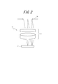
- FIG. 1 is a perspective view of an image display device according to the first embodiment.
- the image display device 10 is configured to include a projection optical system 11 and a pupil expansion optical system 12.
- the direction along the optical axis of the projection optical system 11 is the z direction
- the two directions perpendicular to the z direction and perpendicular to each other are the x direction (first direction) and the y direction (second direction).
- the upper direction is the x direction.
- the lower right direction is the y direction
- the lower left direction is the z direction.
- the projection optical system 11 projects image light corresponding to an arbitrary image at infinity.
- the pupil expansion optical system 12 receives the image light projected by the projection optical system 11, expands the exit pupil, and emits the light. The observer can observe the image by focusing on any position within the projection area PA of the enlarged exit pupil.
- the projection optical system 11 includes an LCD 13 and a collimator 14 composed of a small number of lenses.
- the LCD 13 is also connected to the image control unit 16.
- the LCD 13 displays a display image based on the signal from the image control unit 16.
- another display element such as an organic EL element may be used.
- the collimator 14 converts diffused light emitted from each pixel of the LCD 13 into parallel light.
- the exit pupil 15 formed by the collimator 14 is disposed to coincide with the incident surface of the pupil expansion optical system 12.
- the image control unit 16 in FIG. 1 performs a process in advance to correct distortion of the image generated by the first propagation optical system 22 and the second propagation optical system 24 of the pupil expansion optical system 12.
- the output image signal is output to the LCD 13.
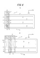
- the pupil expansion optical system 12 includes a polarizer 21, a first propagation optical system 22, a half wave plate 23, and a second propagation optical system 24.
- the polarizer 21, the first propagation optical system 22, the half-wave plate 23, and the second propagation optical system 24 are displayed with a large distance, for the sake of explanation. Are placed close to each other as shown in FIG.
- the polarizer 21 is disposed between the exit pupil 15 of the projection optical system 11 and the projection optical system 11, receives the image light emitted from the projection optical system 11, and emits S-polarized light.
- the first propagation optical system 22 is disposed such that the incident region of a first plane S1 (see FIG. 4) of the first light guide 25 described later and the exit pupil 15 of the projection optical system 11 are combined, and a polarizer An exit pupil projected as S-polarized light by S.21 is enlarged in the x direction and emitted (see reference numeral "Ex").
- the half-wave plate 23 rotates the polarization plane of the image light expanded in the x direction by 90 °.
- the second propagation optical system 24 expands the image light whose polarization plane has been rotated by the half-wave plate 23 in the y direction and emits the light (see reference numeral “Ey”).
- the first propagation optical system 22 includes a first light guide 25, a first diffraction element 26 (first input deflection unit), and a first triangular prism array 27 (first An output deflection unit) is configured to include a first polarization beam splitting film 28.
- the first polarization beam splitting film 28 is vapor-deposited on the first light guide 25 as described later and can not be separated from each other.
- the first light guide 25 is a transparent flat plate having a first plane S1 and a second plane S2 which are parallel and opposite to each other.
- the first diffraction element 26 is bonded to the incident side end of the image light of the second flat surface S2 of the first light guide 25 by a transparent adhesive.
- the first triangular prism array 27 forms the first polarization beam splitting film. It sandwiches and it joins with a transparent adhesive.
- the image light from the projection optical system 11 is incident on the area of the first plane S1 facing the first diffractive element 26, this area is called an incident area, and the first triangular prism of the first plane S1 is
- the area facing the array 27 is an area from which the image light propagating through the first light guide 25 is emitted, and is called an emission area.
- the first polarization beam splitting film 28 is a multilayer film designed to transmit light incident from a substantially perpendicular direction and to reflect most of the light incident from an oblique direction.
- a thin film having low-pass or band-pass spectral reflection characteristics can have such characteristics.
- the first polarization beam splitting film 28 has a transmittance for obliquely incident light, which varies according to the position along the x direction.
- the first polarization beam split film 28 is formed so that the transmittance increases in a geometric progression according to the distance from the one end on the incident region side of the first polarization beam split film 28.
- the distance from the vapor deposition source is arranged to change according to the planar distance from the incident region, and the difference in the distance (difference in film thickness formed into a film) It is possible to form a film by designing in advance to have a desired reflection characteristic at each position according to.
- the first light guide 25 is a rectangular plate long in the x direction (e.g. 60 mm) and short in the y direction (e.g. 20 mm) and has a thickness of several mm (e.g. 3 mm), that is, a length in the z direction It is a member, and quartz (transparent medium) is used as a material.
- quartz transparent medium
- quartz transparent medium
- an AR film is formed on the first plane S1 of the first light guide 25. The AR film suppresses the reflection of image light incident from the vertical direction.
- the first diffraction element 26 is a reflective diffraction element that diffracts the image light incident from the incident region of the first light guide 25 in the x direction.
- the first diffraction element 26 is designed to have high diffraction efficiency in the first diffraction direction with respect to the wavelength of the image light.
- a blazed diffraction grating or the like in which grooves having a sawtooth cross section and extending in the y direction are arranged in the x direction can be used.
- image light incident from the incident region and diffracted and deflected by the first diffraction element 26 is totally reflected by the first plane S1 in the first light guide 25.
- Parameters such as lattice constants are designed to That is, the incident angle of the image light propagating in the first light guide 25 with respect to the first plane S1 is larger than the critical angle.
- the critical angle is 43.6 °.
- the first triangular prism array 27 has a shape in which triangular prisms whose xz cross section is long in the y direction of the triangle are arranged in the x direction.
- Each triangular prism is constituted by a plane in contact with the second plane S2, a plane substantially perpendicular to the second plane S2, and a slope So.
- the triangular prism is made of a transparent medium such as acrylic and formed by injection molding.
- aluminum is vapor-deposited on the slopes So of each triangular prism, and the normal is inclined toward the incident area side.
- the inclination of the inclined surface So is vertically incident on the incident region of the image light, undergoes first-order diffraction in the first diffraction element 26, propagates in the first light guide portion 25, and the first deflection beam splitting film 28
- the light rays passing through and incident on the first triangular prism array 27 are determined to be reflected vertically toward the first plane S1.
- the first light ray b1 vertically incident on the incident area of the first plane S1 (indicated by a broken line in FIG. 4) Is reflected by the first diffraction element 26 joined to the second plane S2 by receiving the first-order diffraction, and the inside of the first light guide 25 is inclined to the first plane S1 parallel to the xz plane. Head to the plane S1 of 1.
- the first light ray b1 directed to the first plane S1 is totally reflected by being incident on the first plane S1 at an angle exceeding the critical angle.
- the totally reflected first light beam b1 travels to the second plane S2 and obliquely enters the first polarization beam splitting film 28 formed on the second plane S2, and transmits only a predetermined amount of light. And the remaining light is reflected.
- the first light beam b1 reflected by the first polarization beam splitting film 28 again enters the first plane S1 at an angle exceeding the critical angle, and is totally reflected. Thereafter, the first light beam b1 is propagated in the x direction of the first light guide 25 while repeating partial reflection in the first polarization beam splitting film 28 and total reflection in the first plane S1. . However, each time the light enters the first polarization beam splitting film 28, the light is transmitted at a predetermined rate and emitted to the first triangular prism array 27.
- the first light ray b1 emitted to the first triangular prism array 27 is perpendicular to the second plane S2 of the first light guide 25 again by the reflection film of the slope So of the first triangular prism array 27. It is reflected by The first light beam b1 reflected in the vertical direction passes through the first light guide 25 and is emitted from the first plane S1 to the outside.
- the half-wave plate 23 (see FIG. 3) is formed in a shape substantially the same size as the emission area of the first plane S1.
- the half-wave plate 23 is disposed with an air gap at a position facing the emission region of the first plane S1. Therefore, a light flux entering the first plane S1 at an incident angle equal to or greater than the critical angle in the first light guide 25 is not totally transmitted through the first plane S1, and total reflection is ensured.
- the half-wave plate 23 rotates the polarization plane of the light beam emitted from the first propagation optical system 22 by 90 degrees.
- the second propagation optical system 24 includes a second light guide unit 31, a second polarization beam split film (not shown), and a second diffraction element 32 (second input deflection unit And a second triangular prism array 33 (second output deflector). Similar to the first propagation optical system 22, these constituent members are in the form of an integrated flat plate, and the width direction of the second propagation optical system 24 and the second light guide portion 31 (the “x direction in FIG. “) And the length direction (“ y direction ”in FIG. 3) are, for example, 50 mm and 110 mm, respectively.
- the length in the longitudinal direction (y direction) of the second polarized beam splitting film in the second propagation optical system 24 is, for example, 100 mm. Further, the length of the second diffraction element 32 in the y direction is, for example, 10 mm.
- the functions of the second light guide 31, the second polarization beam split film, the second diffraction element 32, and the second triangular prism array 33 are respectively the first light guide 25, the first polarization beam split Similar to the film 28, the first diffractive element 26, and the first triangular prism array 27.
- the emission area of the first plane S1 of the first propagation optical system 22 and the incident area of the third plane S3 of the second propagation optical system 24 face each other, and the second propagation optical system 24
- the propagation optical system 24 is disposed in a posture rotated 90 ° around a straight line parallel to the z direction with respect to the first propagation optical system 22 (see FIG. 3). Therefore, the second propagation optical system 24 expands the image light emitted from the first propagation optical system 22 in the y direction and emits it. Thus, the exit pupil is enlarged.
- the second light ray b2 is deflected toward the emission area by the first diffraction element 26, and is totally reflected in the first light guide 25 to the first plane S1 at an angle of a critical angle or more.
- the second light beam b2 totally reflected by the first plane S1 is incident on the second plane S2, and a part of the light quantity is transmitted through the first polarization beam splitting film 28, and the first triangular prism array is formed. It is reflected by 27 slopes So.
- the second light beam b2 reflected by the inclined surface So is transmitted through the first polarization beam splitting film 28 on the second plane S2, passes through the first light guide 25, and is emitted from the first plane S1.
- the second light ray b2 is emitted from the first plane S1 at an emission angle ⁇ o inclined according to the incident angle ⁇ i.
- the diffraction order (m) is ⁇ 1
- the wavelength of image light is ( ⁇ ) 532 nm
- the refractive index (n) of the first triangular prism array 27 is 1.51
- the grating period (d) is 450 nm.
- the relationship between the incident angle ⁇ i and the exit angle ⁇ o is as shown in Table 1.
- the emission angle ⁇ o becomes larger than the incident angle ⁇ i.
- the incident angle ⁇ i and the emission angle ⁇ o become equal.
- the incident angle ⁇ i and the emission angle ⁇ o are equal.
- the incident angle ⁇ i can be made relatively small by enlarging the emission angle ⁇ o. That is, the angle of view of the image light incident from the projection optical system 11 can be reduced.
- FIG. 5A is a view showing a schematic configuration of the projection optical system 11 of the present embodiment, and the configuration is as described with reference to FIG.
- ⁇ 1 indicates the spread of the image light emitted from the LCD 13
- ⁇ 2 indicates the angle of view of the image light projected onto the exit pupil after passing through the collimator 14.
- the angle of view of the image that can be displayed by the image display device is associated with ⁇ 2 that is the angle of view at which the infinite virtual image of the projection optical system 11 at the exit pupil is projected.
- the angle of view ⁇ 4 of the projection optical system 11 is set as shown in FIG.
- the collimator 36 is configured by arranging a large number of optical elements for suppressing the aberration.
- the first propagation optical system 22 and the second propagation optical system 24 of the pupil expansion optical system 12 have the effect of widening the exit angle, that is, the angle of view of the exit pupil It is possible to spread and display an image with a viewing angle larger than that of the incident image light. Therefore, as shown in FIG. 5A, it is possible to reduce the number of lenses or to reduce the size by reducing the focal length.
- FIG. 6 (a) is a view for explaining the propagation of the image light of the pupil magnification optical system 12 of FIG. 1, and FIG. 6 (b) shows the propagation of the image light of the pupil magnification optical system 12a of the conventional example. It is a figure explaining. These figures are views of the pupil magnification optical system 12, 12a in the z direction. Further, in FIG. 6B, components having the same functions as in the first embodiment are indicated by attaching “a” to the same reference numerals as in the first embodiment.
- the image light incident area A3 of the first propagation optical system 22a (that is, the incident area of the first light guiding portion 25a) is widely taken in the y direction in order to prevent vignetting of the light beam and unevenness of the image.
- the width of the y direction is limited within the range in which the image light in the + y direction and the ⁇ y direction overlap, and the emission area A4 of the first propagation optical system 22a (that is, the emission area of the first light guide 25a) is set. I needed it. As a result, most of the image light incident from the projection optical system 11 has been lost by the first propagation optical system 22.
- the angle of view of the image light from the projection optical system 11 is narrow, and the angle of view in the y direction propagating through the first light guide 25 is the projection optical system. Since it is equal to the angle of view of the image light from 11 (because the expansion effect of the emission angle in the first propagation optical system 22 is only the x direction), as shown in FIG. 6A, the first propagation optical system The luminous flux of the image light propagating through the light source 22 is relatively smaller than that in FIG. 6B, for both the luminous flux p1 shifted most in the + y direction and the luminous flux p2 shifted most in the ⁇ y direction.
- the image light incident area A1 of the first propagation optical system 22 (that is, the incident area of the first light guide 25) can be reduced.
- the image light incident from the projection optical system 11 can be propagated to the second propagation optical system 24 as the light flux p3 with high efficiency without being lost by the first propagation optical system 22.
- the entrance pupil of the pupil expansion optical system 12 may be small, the projection optical system 11 can be further downsized.
- the relationship between the incident angle ⁇ i and the exit angle ⁇ o has nonlinearity.
- the image displayed on the LCD 13 is distorted by propagating through the first propagation optical system 22 and the second propagation optical system 24 of the present application. Therefore, the image control unit 16 in FIG. 1 has the opposite distortion in advance so as to correct distortion caused by the first propagation optical system 22 and the second propagation optical system 24 as an image signal of an image to be displayed on the LCD 13.
- the image signal given is output. By doing this, it is possible to display an image without distortion.
- the method of correcting distortion is not limited to this, and, for example, instead of providing the image control unit 16, the LCD according to distortion generated by the first propagation optical system 22 and the second propagation optical system 24 may be used. Distortion can also be corrected by arranging the pixels non-linearly.
- the number of parts of the projection optical system 11 can be reduced and the size thereof can be reduced while securing the size of the display angle of view of the image display device 10.
- the image of the LCD 13 is projected by the projection optical system 11.
- the projection optical system 11 may employ a MEMS mirror.
- the configuration, action, and effects of the projection optical system in this case will be described with reference to FIG.
- the configuration other than the projection optical system is the same as that of the first embodiment.
- the projection optical system of FIG. 7 includes a light source 37, a MEMS mirror 38, and a beam expander 39.
- the light source 37 is a laser light source and can be switched on / off at high speed.
- the MEMS mirror 38 is a mirror element that repeatedly performs two-dimensional scanning at high frequency.
- the light source 37 enlarges the beam diameter according to the mirror surface of the MEMS mirror 38 and irradiates the MEMS mirror 38.
- the beam expander 39 is disposed between the MEMS mirror 38 and the pupil expansion optical system 12 to expand the light beam reflected by the MEMS mirror 38 and to enter the entrance pupil of the pupil expansion optical system 12, ie, the first The light is transmitted to the incident area of the light unit 25.
- the MEMS mirror 38 and the incident area of the first light guide 25 are in an optically conjugate relationship.
- the light source 37 is controlled by a control device (not shown), and emits light at a light emission timing corresponding to an image to be displayed according to the tilting of the MEMS mirror 38.
- the beam expander 39 expands the diameter of the beam reflected by the MEMS mirror 38 corresponding to the incident area of the first light guide 25.
- the exit pupil of the image light having entered the incident region of the first light guide 25 is expanded by the pupil expansion optical system 12 and emitted toward the observer.
- the projection optical system of FIG. 7 when the beam diameter is expanded by the beam expander 39, the emission angle ⁇ 6 of the image light from the beam expander is reduced with respect to the incident angle ⁇ 5. Therefore, in the case of the conventional image display device, in order to obtain a large angle of view in the image display device 10, it is necessary to increase the size of the MEMS mirror 38. However, if the mirror area of the MEMS mirror 38 is increased, generally the frequency of mirror scanning and the deflection angle of the mirror can not be increased.
- the MEMS with a large area in the projection optical system There is no need to use a mirror or to increase the swing angle of the MEMS mirror. Therefore, the projection optical system can be miniaturized. Furthermore, since the MEMS mirror can be scanned at high frequency, it is possible to display an image with a high frame rate.
- FIG. 8 is a view showing a schematic configuration of the image display apparatus according to the second embodiment
- FIG. 8 (a) is a front view
- FIG. 8 (b) is a top view.
- the image display apparatus according to the second embodiment unlike the first embodiment, enlarges the exit pupil only in the x direction by the propagation optical system 42 (first propagation optical system).
- the projection optical system 41 includes a light source 45, a MEMS mirror 46, and a beam expander 47. This configuration is the same as that of the projection optical system of FIG.
- the propagation optical system 42 includes a light guide 48, a diffraction element 49, a triangular prism array 50, and a polarization beam splitting film 51.
- the light guiding portion 48 is a flat member similar to the first light guiding portion 25 of the first embodiment. Further, as in the first diffraction element 26 of the first embodiment, the diffraction element 49 is also provided at the incident side end of the surface (second plane S2) facing the incident area of the image light of the light guide 48 It is provided and has the same function.
- the polarizing beam splitting film 51 and the triangular prism array 50 have the same shape and characteristics as the first polarizing beam splitting film 28 and the first triangular prism array 27 of the first embodiment, Unlike the first embodiment, the light guide portion 48 is provided in a portion other than the incident region of the surface (first plane S1) on the incident side of the image light.
- the image light incident from the projection optical system 41 to the propagation optical system 42 is S-polarized light.
- a polarizer (not shown) may be disposed between the projection optical system 41 and the propagation optical system 42.
- the image light emitted from the projection optical system 41 is incident on the light guide 48 from the first plane S1 of the light guide 48 and of the diffractive element 49 joined to the second plane S2.
- the light is diffracted at the diffractive surface and is propagated in the light guide 48 in the x direction.
- the image light diffracted toward the first plane in the light guide unit 48 passes through the polarization beam splitting film 51 on the first plane S 1 with a part of the light quantity, and the triangular prism array 50
- the light is reflected in a direction perpendicular to the plane S1, passes through the light guide 48, and is emitted from the second plane S2.
- the image light reflected by the polarization beam splitting film 51 travels in the light guiding section 48 while being inclined with respect to the x direction, totally reflected again by the second plane S2, and travels in the first plane direction, Repeat this.
- the image light with the exit pupil expanded in the x direction is emitted.
- the propagation optical system 42 for propagating the image light in one direction
- the diffraction element is used to deflect the image light on the incident side of the light guide 48 and the triangular prism array 50 that functions as a mirror surface is used to deflect the emission side
- the incident light is It has the effect of expanding the angle of view for injection.
- FIG. 9 is a top view showing the incident part of the propagation optical system of FIG. 8A together with the path of the image light.
- the first light ray b1 indicates the image light vertically incident on the light guide 48
- the second light ray b2 indicates the image light incident at the incident angle ⁇ i.
- the emission angle when the second light ray b2 is emitted from the light guide 48 is ⁇ o
- the relationship between the incident angle ⁇ i and the emission angle ⁇ o is as shown in Table 1.
- the diffraction order (m) is ⁇ 1
- the wavelength of image light ( ⁇ ) is 532 nm
- the refractive index (n) of the first triangular prism array 27 is 1.51
- the diffraction is The grating period (d) is 450 nm.
- the emission angle ⁇ o is larger than the incident angle ⁇ i. Therefore, the incident angle ⁇ i can be made relatively small, and the projection optical system 41 can be miniaturized. In addition, since the MEMS mirror 46 may be small, scanning can be performed at a high frequency.
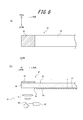
- FIG. 10 shows a modification of the propagation optical system.
- the transmission-type diffraction element 53 is connected to the first plane S ⁇ b> 1 on the incident side of the image light to the light guide 52.
- the polarization beam splitting film 55 and the triangular prism array 54 are provided on the first plane S1 on the light incident side of the light guide 52. Thereby, the image light enters the first plane S1 and is emitted from the second plane S2.
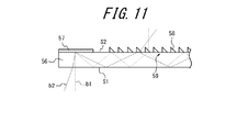
- FIG. 11 is a view showing another modification of the propagation optical system.
- the diffractive element of the reflection type is opposed to the incident area of the image light on the second plane S2 opposed to the first plane S1 on the incident side of the image light of the light guide 56 57 are provided.
- a polarization beam split film 59 is vapor-deposited on the second plane S2, and a triangular prism array 58 composed of a polished surface is further arranged thereon.
- the slopes of the triangular prism array 58 are configured to transmit image light without being aluminum-deposited.
- a part of the image light incident on the second plane S2 of the light guide and transmitted through the polarization beam splitting film 59 is refracted by the slope of the triangular prism and deflected, and is emitted in a direction substantially perpendicular to the second plane Be done.
- FIG. 12 is a view showing a further modification of the propagation optical system.
- the incident region of the first plane S1 on the light incident side of the light guide 60 is notched obliquely, and the normal is inclined to be inclined in the x direction,
- a transmissive diffraction element 61 is provided on the slope.
- the polarization beam splitting film 63 is deposited on the other part of the first plane S1, and the triangular prism array 62 is connected thereon.
- the image light incident on this propagation optical system is diffracted by the diffraction element 61 formed on the slope and deflected, and propagates in the light guide 60 as in the second embodiment while the second plane S2 is formed. Are ejected substantially perpendicularly to the second plane S2.
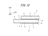
- FIG. 13 is a view showing a cross section of the pupil expansion optical system of the third embodiment configured as described above, together with the optical path of the image light.
- the configuration of FIG. 13 is similar to the configuration of the pupil expansion optical system 12 of the first embodiment, so the same components are denoted by the same reference numerals. Components denoted by the same reference numerals have the same configuration as the first embodiment unless otherwise described.
- the first propagation optical system 22 and the second propagation optical system 24 are transmission propagation optical systems similar to the propagation optical system 48 shown in FIG. 9 in which the incident surface and the exit surface are different. is there.
- a half wave plate 23 is provided between the first propagation optical system 22 and the second propagation optical system 24.
- the first light guiding portion 25 of the first propagation optical system 22 is the same as the light guiding portion 48 of FIG. 9 of the second embodiment except for the first polarization beam splitting film 28. It differs only in that it is formed inside the surface on the incident side of the image light.
- Such a first light guide 25 deposits a polarized beam split film on one surface of one of two transparent plate-like members, and the other member on the surface on which the polarized beam split surface is formed. Can be formed by bonding them with a transparent adhesive or the like.
- the image light incident on the first light guide section 25 is diffracted by the first diffraction grating 26, a part of the light quantity is transmitted by the first polarization beam split film 28, and the remaining light quantity is reflected. It is totally reflected in the plane S2 of. Then, the light beam is propagated in the x direction while repeating reflection between the first deflection beam split film 28 and the second plane S2. Therefore, in the present embodiment, the plane on which the first polarization beam splitting film 28 is formed corresponds to the first plane S1.
- the image light transmitted through the first deflection beam splitting film 28 is reflected by the first triangular prism array 27, passes through the inside of the first light guiding portion 25, and is transmitted from the second plane S2 to the second plane. Ejected in a substantially vertical direction.
- the image light emitted from the second plane S2 has its polarization direction rotated by 90 degrees by the half-wave plate 23, and enters the second propagation optical system 24 as S-polarization.
- the second propagation optical system 24 is also configured in the same manner as the first propagation optical system 22 of the present embodiment except for the size and direction. Thereby, the image light incident on the second propagation optical system 24 and diffracted by the second diffraction element 32 is repeatedly reflected in the second light guide portion 31 while propagating the image light in the y direction.
- the light is emitted from a fourth plane S4 opposed to the surface on the incident side.
- the present embodiment as in the first embodiment, it is possible to provide an image display apparatus in which the exit pupil is enlarged in the x direction and the y direction. Then, in the first propagation optical system 22 and the second propagation optical system 24, the deflection on the incident side is performed by diffraction, and the deflection on the emission side is performed by reflection, so that the display angle of view of the image display device is secured. At the same time, the number of parts of the projection optical system can be reduced or miniaturized.
- first and second propagation optical systems are not limited to the illustrated ones, and any system using a diffractive element for the incident side polarization and a reflective or refractive element for the emission side polarization is included in the scope of the present invention. .
- image display device 11 projection optical system 12 pupil magnification optical system 13 LCD 14 collimator 15 exit pupil 16 image control unit 21 polarizer 22 first propagation optical system 23 half wave plate 24 second propagation optical system 25 first light guide section 26 first diffractive element 27 first triangle Prism array 28 First polarized beam split film 31 Second light guide 32 Second diffractive element 33 Second triangular prism array 36 Collimator 37, 45 Light source 38, 46 MEMS mirror 39, 47 Beam expander 41 Projection optics System 42 propagation optical system 48, 52, 56, 60 Light guide 49, 53, 57, 61 Diffraction element 50, 54, 58, 62, triangular prism array 51, 55, 59, 63 Polarized beam splitting film
Landscapes
- Physics & Mathematics (AREA)
- General Physics & Mathematics (AREA)
- Optics & Photonics (AREA)
- Engineering & Computer Science (AREA)
- Microelectronics & Electronic Packaging (AREA)
- Projection Apparatus (AREA)
Priority Applications (1)
| Application Number | Priority Date | Filing Date | Title |
|---|---|---|---|
| US15/253,793 US20160370693A1 (en) | 2014-03-27 | 2016-08-31 | Image display device |
Applications Claiming Priority (2)
| Application Number | Priority Date | Filing Date | Title |
|---|---|---|---|
| JP2014066604A JP6442149B2 (ja) | 2014-03-27 | 2014-03-27 | 画像表示装置 |
| JP2014-066604 | 2014-03-27 |
Related Child Applications (1)
| Application Number | Title | Priority Date | Filing Date |
|---|---|---|---|
| US15/253,793 Continuation US20160370693A1 (en) | 2014-03-27 | 2016-08-31 | Image display device |
Publications (1)
| Publication Number | Publication Date |
|---|---|
| WO2015145963A1 true WO2015145963A1 (ja) | 2015-10-01 |
Family
ID=54194521
Family Applications (1)
| Application Number | Title | Priority Date | Filing Date |
|---|---|---|---|
| PCT/JP2015/000877 Ceased WO2015145963A1 (ja) | 2014-03-27 | 2015-02-23 | 画像表示装置 |
Country Status (3)
| Country | Link |
|---|---|
| US (1) | US20160370693A1 (https=) |
| JP (1) | JP6442149B2 (https=) |
| WO (1) | WO2015145963A1 (https=) |
Cited By (3)
| Publication number | Priority date | Publication date | Assignee | Title |
|---|---|---|---|---|
| CN106101512A (zh) * | 2016-08-11 | 2016-11-09 | 李炳华 | 一种半球面多角度智能拍摄系统及方法 |
| CN107870440A (zh) * | 2016-09-26 | 2018-04-03 | 精工爱普生株式会社 | 光束直径放大装置和显示装置 |
| CN108738358A (zh) * | 2017-02-22 | 2018-11-02 | 鲁姆斯有限公司 | 导光光学组件 |
Families Citing this family (52)
| Publication number | Priority date | Publication date | Assignee | Title |
|---|---|---|---|---|
| US10073264B2 (en) | 2007-08-03 | 2018-09-11 | Lumus Ltd. | Substrate-guide optical device |
| US10261321B2 (en) | 2005-11-08 | 2019-04-16 | Lumus Ltd. | Polarizing optical system |
| IL232197B (en) | 2014-04-23 | 2018-04-30 | Lumus Ltd | Compact head-up display system |
| IL235642B (en) | 2014-11-11 | 2021-08-31 | Lumus Ltd | A compact head-up display system is protected by an element with a super-thin structure |
| EP3062142B1 (en) | 2015-02-26 | 2018-10-03 | Nokia Technologies OY | Apparatus for a near-eye display |
| JP6597196B2 (ja) * | 2015-11-05 | 2019-10-30 | セイコーエプソン株式会社 | 虚像表示措置 |
| JP7187022B2 (ja) * | 2016-10-09 | 2022-12-12 | ルムス エルティーディー. | 長方形導波路を使用する開口乗算器 |
| CN113031165B (zh) | 2016-11-08 | 2023-06-02 | 鲁姆斯有限公司 | 导光装置、其光学组件及其对应的生产方法 |
| US10650552B2 (en) | 2016-12-29 | 2020-05-12 | Magic Leap, Inc. | Systems and methods for augmented reality |
| EP3343267B1 (en) | 2016-12-30 | 2024-01-24 | Magic Leap, Inc. | Polychromatic light out-coupling apparatus, near-eye displays comprising the same, and method of out-coupling polychromatic light |
| US10409066B2 (en) * | 2017-01-19 | 2019-09-10 | Coretronic Corporation | Head-mounted display device with waveguide elements |
| CN117572644A (zh) | 2017-03-22 | 2024-02-20 | 鲁姆斯有限公司 | 用于生产光导光学元件的方法和光学系统 |
| IL251645B (en) | 2017-04-06 | 2018-08-30 | Lumus Ltd | Waveguide and method of production |
| AU2018270948B2 (en) * | 2017-05-16 | 2022-11-24 | Magic Leap, Inc. | Systems and methods for mixed reality |
| JP7222968B2 (ja) * | 2017-07-13 | 2023-02-15 | シーリアル テクノロジーズ ソシエテ アノニム | 視野を拡大するためのディスプレイデバイス |
| US10578870B2 (en) | 2017-07-26 | 2020-03-03 | Magic Leap, Inc. | Exit pupil expander |
| DE102017122353A1 (de) | 2017-09-26 | 2019-03-28 | Carl Zeiss Ag | Optische Übertragungsanordnung zum Übertragen eines Quellbildes |
| JP7282090B2 (ja) | 2017-12-10 | 2023-05-26 | マジック リープ, インコーポレイテッド | 光学導波管上の反射防止性コーティング |
| CN111712751B (zh) | 2017-12-20 | 2022-11-01 | 奇跃公司 | 用于增强现实观看设备的插入件 |
| US10551544B2 (en) | 2018-01-21 | 2020-02-04 | Lumus Ltd. | Light-guide optical element with multiple-axis internal aperture expansion |
| EP4415355A3 (en) | 2018-03-15 | 2024-09-04 | Magic Leap, Inc. | Image correction due to deformation of components of a viewing device |
| WO2019224764A1 (en) | 2018-05-23 | 2019-11-28 | Lumus Ltd. | Optical system including light-guide optical element with partially-reflective internal surfaces |
| CN112601975B (zh) | 2018-05-31 | 2024-09-06 | 奇跃公司 | 雷达头部姿势定位 |
| WO2020010097A1 (en) | 2018-07-02 | 2020-01-09 | Magic Leap, Inc. | Pixel intensity modulation using modifying gain values |
| US11856479B2 (en) | 2018-07-03 | 2023-12-26 | Magic Leap, Inc. | Systems and methods for virtual and augmented reality along a route with markers |
| JP7374981B2 (ja) | 2018-07-10 | 2023-11-07 | マジック リープ, インコーポレイテッド | クロス命令セットアーキテクチャプロシージャ呼出のためのスレッドウィービング |
| US11598651B2 (en) | 2018-07-24 | 2023-03-07 | Magic Leap, Inc. | Temperature dependent calibration of movement detection devices |
| WO2020023543A1 (en) | 2018-07-24 | 2020-01-30 | Magic Leap, Inc. | Viewing device with dust seal integration |
| EP4650919A3 (en) | 2018-08-02 | 2026-01-21 | Magic Leap, Inc. | A viewing system with interpupillary distance compensation based on head motion |
| EP3830631A4 (en) | 2018-08-03 | 2021-10-27 | Magic Leap, Inc. | DRIFT CORRECTION BASED ON UNMERGED LAYING OF MELTED LAYING OF A TOTEM IN A USER INTERACTION SYSTEM |
| JP7487176B2 (ja) | 2018-08-22 | 2024-05-20 | マジック リープ, インコーポレイテッド | 患者視認システム |
| JP7543274B2 (ja) | 2018-12-21 | 2024-09-02 | マジック リープ, インコーポレイテッド | 導波管内の全内部反射を助長するための空気ポケット構造 |
| WO2020174433A1 (en) | 2019-02-28 | 2020-09-03 | Lumus Ltd. | Compact collimated image projector |
| EP3939030B1 (en) | 2019-03-12 | 2025-10-29 | Magic Leap, Inc. | Registration of local content between first and second augmented reality viewers |
| KR20210151782A (ko) | 2019-04-15 | 2021-12-14 | 루머스 리미티드 | 광-유도 광학 소자 제조 방법 |
| CN120812326A (zh) | 2019-05-01 | 2025-10-17 | 奇跃公司 | 内容提供系统和方法 |
| IL289411B2 (en) | 2019-06-27 | 2025-07-01 | Lumus Ltd | Device and methods for eye tracking based on eye imaging using a light-conducting optical component |
| WO2021009766A1 (en) | 2019-07-18 | 2021-01-21 | Lumus Ltd. | Encapsulated light-guide optical element |
| WO2021021670A1 (en) | 2019-07-26 | 2021-02-04 | Magic Leap, Inc. | Systems and methods for augmented reality |
| US12033081B2 (en) | 2019-11-14 | 2024-07-09 | Magic Leap, Inc. | Systems and methods for virtual and augmented reality |
| EP4058979A4 (en) | 2019-11-15 | 2023-01-11 | Magic Leap, Inc. | VISUALIZATION SYSTEM FOR USE IN A SURGICAL ENVIRONMENT |
| CA3155597C (en) | 2019-12-08 | 2023-02-14 | Lumus Ltd. | Optical systems with compact image projector |
| DE212021000276U1 (de) | 2020-05-12 | 2022-11-03 | Lumus Ltd. | Drehbarer Lichtleiter |
| WO2022044006A1 (en) | 2020-08-26 | 2022-03-03 | Lumus Ltd. | Generation of color images using white light as source |
| CN115989453B (zh) | 2020-08-30 | 2026-04-28 | 鲁姆斯有限公司 | 具有中间图像平面的反射slm图像投影仪 |
| IL313859B2 (en) | 2021-03-01 | 2025-11-01 | Lumus Ltd | Optical system with compact coupling from a projector into a waveguide |
| JP7716673B2 (ja) * | 2021-03-05 | 2025-08-01 | パナソニックIpマネジメント株式会社 | 光学系、及び、画像表示装置 |
| KR20240097972A (ko) | 2021-05-19 | 2024-06-27 | 루머스 리미티드 | 액티브 광학 엔진 |
| KR102676604B1 (ko) | 2021-07-04 | 2024-06-18 | 루머스 리미티드 | 시야의 다양한 부분을 제공하는 적층형 도광 요소를 갖는 디스플레이 |
| JP2024532842A (ja) | 2021-08-23 | 2024-09-10 | ルーマス リミテッド | 埋め込まれた結合反射器を有する複合導光光学素子の作製方法 |
| KR20250053044A (ko) | 2022-08-18 | 2025-04-21 | 루머스 리미티드 | 편광 반사굴절 시준기를 갖는 이미지 프로젝터 |
| JP2024089261A (ja) * | 2022-12-21 | 2024-07-03 | 株式会社デンソー | 光学部材 |
Citations (5)
| Publication number | Priority date | Publication date | Assignee | Title |
|---|---|---|---|---|
| WO2006025317A1 (ja) * | 2004-08-31 | 2006-03-09 | Nikon Corporation | 光束径拡大光学系及び画像表示装置 |
| JP2010044326A (ja) * | 2008-08-18 | 2010-02-25 | Sony Corp | 画像表示装置 |
| JP2013037095A (ja) * | 2011-08-05 | 2013-02-21 | Seiko Epson Corp | 虚像表示装置 |
| WO2013135943A1 (en) * | 2012-03-16 | 2013-09-19 | Nokia Corporation | Image providing apparatus and method |
| JP2014013968A (ja) * | 2012-07-03 | 2014-01-23 | Sony Corp | 画像信号処理装置、および画像信号処理方法、並びにプログラム |
Family Cites Families (17)
| Publication number | Priority date | Publication date | Assignee | Title |
|---|---|---|---|---|
| ATE254291T1 (de) * | 1998-04-02 | 2003-11-15 | Elop Electrooptics Ind Ltd | Optische holographische vorrichtungen |
| WO2003027754A1 (en) * | 2001-09-25 | 2003-04-03 | Cambridge Flat Projection Displays | Flat-panel projection display |
| IL148804A (en) * | 2002-03-21 | 2007-02-11 | Yaacov Amitai | Optical device |
| EP1639394A2 (en) * | 2003-06-10 | 2006-03-29 | Elop Electro-Optics Industries Ltd. | Method and system for displaying an informative image against a background image |
| EP1922579B1 (en) * | 2005-09-07 | 2015-08-19 | BAE Systems PLC | A projection display with two plate-like, co-planar waveguides including gratings |
| DE602006010215D1 (de) * | 2005-09-07 | 2009-12-17 | Bae Systems Plc | Projektionsanzeige mit einem stabartigen wellenleiter mit rechteckigem querschnitt und einem plattenartigen wellenleiter, die jeweils ein beugungsgitter aufweisen |
| EP3667399A1 (en) * | 2007-06-04 | 2020-06-17 | Magic Leap, Inc. | A diffractive beam expander |
| WO2009077772A1 (en) * | 2007-12-18 | 2009-06-25 | Bae Systems Plc | Improvemements in or relating to display projectors |
| EP2225601A1 (en) * | 2007-12-18 | 2010-09-08 | BAE Systems PLC | Improvements in or relating to projection displays |
| US8369019B2 (en) * | 2008-04-14 | 2013-02-05 | Bae Systems Plc | Waveguides |
| US7613373B1 (en) * | 2008-07-03 | 2009-11-03 | Microvision, Inc. | Substrate guided relay with homogenizing input relay |
| US7570859B1 (en) * | 2008-07-03 | 2009-08-04 | Microvision, Inc. | Optical substrate guided relay with input homogenizer |
| EP2329302B1 (en) * | 2008-09-16 | 2019-11-06 | BAE Systems PLC | Improvements in or relating to waveguides |
| WO2010067116A1 (en) * | 2008-12-12 | 2010-06-17 | Bae Systems Plc | Improvements in or relating to waveguides |
| JP5901192B2 (ja) * | 2011-09-13 | 2016-04-06 | オリンパス株式会社 | 光学機構 |
| JP5884502B2 (ja) * | 2012-01-18 | 2016-03-15 | ソニー株式会社 | ヘッドマウントディスプレイ |
| US9411210B2 (en) * | 2013-03-28 | 2016-08-09 | Panasonic Intellectual Property Management Co., Ltd. | Image display device |
-
2014
- 2014-03-27 JP JP2014066604A patent/JP6442149B2/ja not_active Expired - Fee Related
-
2015
- 2015-02-23 WO PCT/JP2015/000877 patent/WO2015145963A1/ja not_active Ceased
-
2016
- 2016-08-31 US US15/253,793 patent/US20160370693A1/en not_active Abandoned
Patent Citations (5)
| Publication number | Priority date | Publication date | Assignee | Title |
|---|---|---|---|---|
| WO2006025317A1 (ja) * | 2004-08-31 | 2006-03-09 | Nikon Corporation | 光束径拡大光学系及び画像表示装置 |
| JP2010044326A (ja) * | 2008-08-18 | 2010-02-25 | Sony Corp | 画像表示装置 |
| JP2013037095A (ja) * | 2011-08-05 | 2013-02-21 | Seiko Epson Corp | 虚像表示装置 |
| WO2013135943A1 (en) * | 2012-03-16 | 2013-09-19 | Nokia Corporation | Image providing apparatus and method |
| JP2014013968A (ja) * | 2012-07-03 | 2014-01-23 | Sony Corp | 画像信号処理装置、および画像信号処理方法、並びにプログラム |
Cited By (5)
| Publication number | Priority date | Publication date | Assignee | Title |
|---|---|---|---|---|
| CN106101512A (zh) * | 2016-08-11 | 2016-11-09 | 李炳华 | 一种半球面多角度智能拍摄系统及方法 |
| CN106101512B (zh) * | 2016-08-11 | 2021-08-13 | 李炳华 | 一种半球面多角度智能拍摄系统及方法 |
| CN107870440A (zh) * | 2016-09-26 | 2018-04-03 | 精工爱普生株式会社 | 光束直径放大装置和显示装置 |
| CN108738358A (zh) * | 2017-02-22 | 2018-11-02 | 鲁姆斯有限公司 | 导光光学组件 |
| CN108738358B (zh) * | 2017-02-22 | 2021-03-26 | 鲁姆斯有限公司 | 导光光学组件 |
Also Published As
| Publication number | Publication date |
|---|---|
| US20160370693A1 (en) | 2016-12-22 |
| JP2015191032A (ja) | 2015-11-02 |
| JP6442149B2 (ja) | 2018-12-19 |
Similar Documents
| Publication | Publication Date | Title |
|---|---|---|
| JP6442149B2 (ja) | 画像表示装置 | |
| TWI913006B (zh) | 包括具有二維擴展的光導光學元件的光學系統 | |
| CN111183393B (zh) | 增强现实显示器 | |
| CN107209372B (zh) | 显示系统 | |
| TWI858170B (zh) | 採用散光光學器件和像差補償的顯示器 | |
| WO2015136850A1 (ja) | 表示装置 | |
| US9880383B2 (en) | Display device | |
| US10012833B2 (en) | Displaying apparatus including optical image projection system and two plate-shaped optical propagation systems | |
| JP6265805B2 (ja) | 画像表示装置 | |
| WO2014009717A1 (en) | Head up displays | |
| US20210165226A1 (en) | Image display device | |
| WO2019187332A1 (ja) | 導光板、導光板製造方法及び映像表示装置 | |
| US20250020940A1 (en) | Method and system for fiber scanning projector with angled eyepiece | |
| JP5989092B2 (ja) | 光学素子 | |
| TWI571656B (zh) | 光源模組與顯示裝置 | |
| JP6296841B2 (ja) | 表示装置 | |
| CN115461667B (zh) | 光学装置 | |
| CN105824126B (zh) | 光源模块及显示装置 | |
| TW202613628A (zh) | 包括具有二維擴展的光導光學元件的光學系統及用於製造供光學系統中使用的光導光學元件的方法 |
Legal Events
| Date | Code | Title | Description |
|---|---|---|---|
| 121 | Ep: the epo has been informed by wipo that ep was designated in this application |
Ref document number: 15767851 Country of ref document: EP Kind code of ref document: A1 |
|
| NENP | Non-entry into the national phase |
Ref country code: DE |
|
| 122 | Ep: pct application non-entry in european phase |
Ref document number: 15767851 Country of ref document: EP Kind code of ref document: A1 |