WO2015115403A1 - 通信回路 - Google Patents
通信回路 Download PDFInfo
- Publication number
- WO2015115403A1 WO2015115403A1 PCT/JP2015/052148 JP2015052148W WO2015115403A1 WO 2015115403 A1 WO2015115403 A1 WO 2015115403A1 JP 2015052148 W JP2015052148 W JP 2015052148W WO 2015115403 A1 WO2015115403 A1 WO 2015115403A1
- Authority
- WO
- WIPO (PCT)
- Prior art keywords
- variable capacitance
- capacitance element
- output terminal
- rfic
- terminal
- Prior art date
- Legal status (The legal status is an assumption and is not a legal conclusion. Google has not performed a legal analysis and makes no representation as to the accuracy of the status listed.)
- Ceased
Links
Images




Classifications
-
- H—ELECTRICITY
- H04—ELECTRIC COMMUNICATION TECHNIQUE
- H04B—TRANSMISSION
- H04B5/00—Near-field transmission systems, e.g. inductive or capacitive transmission systems
- H04B5/20—Near-field transmission systems, e.g. inductive or capacitive transmission systems characterised by the transmission technique; characterised by the transmission medium
- H04B5/24—Inductive coupling
-
- H—ELECTRICITY
- H04—ELECTRIC COMMUNICATION TECHNIQUE
- H04B—TRANSMISSION
- H04B5/00—Near-field transmission systems, e.g. inductive or capacitive transmission systems
- H04B5/70—Near-field transmission systems, e.g. inductive or capacitive transmission systems specially adapted for specific purposes
- H04B5/77—Near-field transmission systems, e.g. inductive or capacitive transmission systems specially adapted for specific purposes for interrogation
Definitions
- the present invention relates to a communication circuit used in an RFID (Radio Frequency Identification) system or a near field communication (NFC) system.
- RFID Radio Frequency Identification
- NFC near field communication
- NFC is one of the short-range wireless communication standards using the HF band, and is installed in various terminals including mobile communication terminals.
- an RF IC for NFC is built in the terminal body, and the RFIC for NFC is connected to an NFC antenna coil that is also built in the terminal body.
- a capacitive element is connected to the antenna coil so as to resonate at a communication frequency, and an antenna resonant circuit is configured by the capacitive element and the antenna coil.
- the antenna resonant circuit, the NFC RFIC, and the like constitute an NFC wireless communication circuit.
- the communication frequency of the NFC wireless communication circuit is determined in advance, but the resonance frequency of the antenna resonance circuit to be adjusted slightly differs depending on the use conditions and manufacturing variations.
- the circuit configuration as the resonance circuit of the antenna resonance circuit changes between the reader / writer mode and the card mode. Therefore, in order to maintain a predetermined resonance frequency in either mode, it is necessary to adjust the resonance frequency according to the mode.
- the usage conditions vary depending on the mounting environment of the antenna coil.
- the resonance frequency of the antenna resonance circuit changes depending on whether or not metal is present near the antenna coil.
- Patent Document 1 discloses that a capacitor of an antenna resonance circuit is configured by a variable capacitance element whose capacitance value can be changed by an applied voltage. Further, Patent Document 2 discloses a circuit in which the entire capacitance value is switched by selectively connecting a plurality of capacitors.
- FIG. 8 shows an example of a communication circuit disclosed in Patent Document 2.
- the non-contact IC unit 47 includes a non-contact IC chip, a capacitor Cin and parallel capacitors Ca to Cc, an antenna parallel capacitor unit having switches SW1 to SW3, and an antenna L1.
- the capacities of the capacitor Cin and the parallel capacitors Ca to Cc are fixed values.
- SW1 to SW3 are circuits for switching the connection of the parallel capacitors Ca to Cc ON / OFF.
- the control IC 62 with a nonvolatile memory is connected to the non-contact IC unit 47.
- the control IC 62 controls the switches SW1 to SW3 of the non-contact IC unit 47 and switches the switches SW1 to SW3 on / off.
- the circuit configuration is simple if only the first frequency and the second frequency are switched.
- the control voltage to the variable capacitance diode needs to be multivalued, so that the circuit becomes complicated.
- a terminal for inputting and outputting a signal and data for adjusting the resonance frequency of the antenna resonance circuit, and A plurality of lines for transmitting them is required. Further, in order to switch a plurality of capacitors and adjust the capacitance value in a minute step, a large number of capacitors and a switching multistage switch are required. As a result, the circuit configuration becomes complicated and the size of the IC also increases.
- An object of the present invention is to make it possible to adjust the resonance frequency of the antenna resonance circuit to multiple values without increasing the number of terminals for inputting and outputting signals and data and the lines for transmitting them, and without increasing the number of capacitive elements. Therefore, an object of the present invention is to provide a communication circuit that eliminates the complexity and size of the circuit configuration.
- a communication circuit of the present invention includes an RFIC including a transmission / reception signal input / output terminal and a general-purpose input / output terminal, an antenna coil connected to the transmission / reception signal input / output terminal, the antenna coil connected to the antenna coil, A variable capacitance element that changes a resonance frequency of an antenna resonance circuit including a coil, and the variable capacitance element is an element that changes a capacitance value according to a magnitude of an applied control voltage.
- An application terminal for applying a control voltage is connected to the general-purpose input / output terminal of the RFIC, and the RFIC includes control means for outputting a PWM signal from the general-purpose input / output terminal, and the control for the variable capacitance element. The voltage is controlled by the duty of the PWM signal.
- the capacitance value of the variable capacitance element can be easily adjusted to multiple values, and therefore the resonance frequency of the antenna resonance circuit can be easily adjusted to multiple values. Can be adjusted. Further, since the general-purpose input / output terminal of the RFIC is used and there is no need to provide an IC for applying a control voltage such as a control IC, it is possible to eliminate the complexity and increase in size of the circuit configuration.
- a resistor is connected in series between the general-purpose input / output terminal and the variable capacitance element. Therefore, the ripple of the control voltage to the variable capacitance element can be effectively suppressed, and the carrier frequency of the PWM signal can be lowered.
- a communication circuit includes an RFIC including a transmission / reception signal input / output terminal, an antenna coil connected to the transmission / reception signal input / output terminal, an antenna resonance connected to the antenna coil and including the antenna coil.
- a variable capacitance element that changes a resonance frequency of the circuit; and a control IC connected to the variable capacitance element, wherein the variable capacitance element is an element whose capacitance value changes according to the magnitude of an applied control voltage.
- An application terminal for applying the control voltage to the variable capacitance element is connected to a general-purpose input / output terminal of the control IC, and the control IC includes control means for outputting a PWM signal from the general-purpose input / output terminal. The control voltage for the variable capacitance element is controlled by the duty of the PWM signal.
- the capacitance value of the variable capacitance element can be easily adjusted to multiple values, and therefore the resonance frequency of the antenna resonance circuit can be easily adjusted to multiple values. Can be adjusted.
- a resistor is connected in series between the general-purpose input / output terminal of the control IC and the variable capacitance element.
- the resonance frequency of the antenna resonance circuit can be easily adjusted to multiple values, the number of parts can be reduced, the signal line can be routed very easily, and the communication circuit can be reduced in size and simplified. .
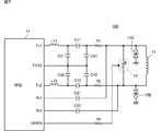
- FIG. 1 is a circuit diagram of a communication circuit 101 according to the first embodiment.
- FIG. 2 is an overall circuit diagram of the inside of the variable capacitance element 14.
- 3A and 3B are diagrams showing the relationship between the output voltage waveform of the GPIO0 terminal and the voltage applied between the ports P13 and P14 of the variable capacitance element 14.
- FIG. 4A and FIG. 4B are diagrams showing characteristics of capacitance value change with respect to the control amount of the variable capacitance element 14.
- FIG. 5 is a circuit diagram of the communication circuit 102 of the second embodiment.
- FIG. 6 is a voltage waveform diagram showing the action of the resistor R4.
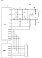
- FIG. 7 is a circuit diagram of the communication circuit 103 according to the third embodiment.
- FIG. 8 shows an example of a communication circuit disclosed in Patent Document 2.
- FIG. 1 is a circuit diagram of a communication circuit 101 according to the first embodiment.
- the communication circuit 101 is an example of an NFC module.
- the communication circuit 101 includes an RFIC 11, an antenna coil 13, and a variable capacitance element 14.
- the RFIC 11 includes transmission signal terminals Tx1 and Tx2, a transmission signal ground terminal TVSS terminal, reception signal terminals Rx1 and Rx2, and a general purpose input / output (GPIO) terminal.
- the RFIC 11 includes control means for setting the GPIO terminal as an output port, switching the output voltage between H level and L level, and controlling the duty to output a PWM signal.
- the RFIC 11 performs modulation and demodulation between the baseband signal and the high frequency signal.
- the RFIC 11 also inputs and outputs data including communication data.
- variable capacitance element 14 includes a control terminal (application terminal for applying a control voltage).
- the variable capacitance element 14 includes a capacitance element whose capacitance value is determined according to a control voltage (bias voltage) and a resistance element that applies a voltage input to the control terminal to the capacitance element.
- the GPIO0 terminal which is one of the GPIO terminals of the RFIC 11, is connected to the control terminal of the variable capacitance element 14.
- the variable capacitance element 14 is connected to the antenna coil 13 in parallel. Between the two transmission signal terminals Tx1, Tx2 of the RFIC 11 and the variable capacitance element 14, a filter circuit and a matching circuit are provided by inductors L11, L12, capacitors C11, C12, C31, C32, C41, C42 and resistors R1, R2. It has been. Capacitors C 21 and C 22 are connected between the two reception signal terminals Rx 1 and Rx 2 of the RFIC 11 and the variable capacitance element 14.
- the variable capacitance element 14 constitutes an antenna resonance circuit which is an LC parallel resonance circuit together with the antenna coil 13, and sets the resonance frequency of the antenna resonance circuit to a predetermined frequency.
- the antenna coil 13 performs near field communication mainly by magnetic coupling with the antenna of the communication partner.
- the RFIC 11 when the communication circuit operates in the card mode, the RFIC 11 operates passively. Therefore, the power supply voltage is generated from the input signals to the reception signal terminals Rx1 and Rx2, the reception signal is read, and the transmission signal terminals Tx1 and Tx2 are connected during transmission. Load modulation is performed on a circuit (load) that is connected. Further, for example, when the communication circuit operates in the reader / writer mode, the RFIC 11 performs an active operation. Therefore, the transmission signal terminals Rx1 and Rx2 are opened at the time of transmission to transmit transmission signals from the transmission signal terminals Tx1 and Tx2, and at the time of reception.
- the transmission signal terminals Tx1 and Tx2 are opened, and reception signals are input from the reception signal terminals Rx1 and Rx2.
- the impedance of the communication circuit as viewed from the RFIC 11 to the antenna coil 13 changes according to the operation mode.
- the variable capacitance element 14 is controlled so that the resonance frequency of the antenna resonance circuit is optimized in accordance with the operation mode (so that the impedance when the antenna coil side is viewed from the RFIC 11 is matched).
- ESD protection elements 17A and 17B are connected to both ends of the antenna coil 13 between the antenna coil 13 and the ground. These ESD protection elements 17A and 17B allow an electrostatic discharge surge entering from the antenna coil 13 to escape to the ground and prevent an overvoltage from being applied to the RFIC 11.
- FIG. 2 is an overall circuit diagram of the inside of the variable capacitance element 14.
- the variable capacitance element 14 includes capacitance elements C1 to C6 and resistance elements R11 to R17.
- a control voltage is applied to both ends of the capacitance elements C1 to C6 via resistance elements R11 to R17.
- the resistance values of the resistance elements R11 to R17 are equal.
- These RF resistance elements R11 to R17 apply a control voltage to the capacitive elements C1 to C6 and suppress leakage of an RF signal applied between the ports P11 and P12 to the ports P13 and P14.
- the capacitive elements C1 to C6 are ferroelectric capacitors in which a ferroelectric film is sandwiched between a pair of opposed electrodes. Since the amount of polarization of the ferroelectric film changes according to the strength of the applied electric field and the apparent dielectric constant changes, the capacitance value is determined by the control voltage.
- a dielectric material having a high dielectric constant As a thin film material used for the ferroelectric film, a dielectric material having a high dielectric constant is used. Specifically, a dielectric material having a high dielectric constant is used as a thin film material used for the ferroelectric film. Specifically, perovskite compounds such as (Ba, Sr) TiO 3 (BST), SrTiO 3 , BaTiO 3 , Pb (Zr, Ti) O 3 , bismuth layered compounds such as SrBi 4 Ti 4 O 15 , etc. are used. be able to.
- Capacitance elements C1 to C6 and resistors R11 to R17 are connected between the ports P13 and P14 of the variable capacitance element 14.
- the CR circuit using the capacitance elements C1 to C6 and the resistance elements R11 to R17 is a smoothing circuit and a low-pass circuit. Acts as a filter. Therefore, even if the voltage applied between the ports P13 and P14 is a rectangular wave voltage signal, the control voltage applied to the capacitive elements C1 to C6 is a smoothed voltage.
- FIG. 3A and 3B are diagrams showing the relationship between the output voltage waveform of the GPIO0 terminal and the voltage applied between the ports P13 and P14 of the variable capacitance element 14.
- FIG. 3A shows an example in which the duty ratio of the output voltage at the GPIO0 terminal is small
- FIG. 3B shows an example in which the duty ratio of the output voltage at the GPIO0 terminal is large.
- variable capacitance element 14 By outputting a PWM-modulated rectangular wave from the GPIO0 terminal, a voltage corresponding to the average value of the rectangular wave is applied to the variable capacitance element 14 as a control voltage. Therefore, the capacitance value of the variable capacitor 14 can be controlled according to the duty ratio of the output voltage of the GPIO0 terminal.
- 4 (A) and 4 (B) are diagrams showing characteristics of capacitance value change with respect to the control amount of the variable capacitance element 14.
- 4A shows the relationship between the output voltage of the GPIO0 terminal and the capacitance value with respect to the duty ratio
- FIG. 4B shows the relationship between the variable capacitance element 14 and the capacitance value with respect to the DC control voltage.
- the capacitance value is determined in the range of 60.0 pF to 38.0 pF.
- the output voltage of the GPIO0 terminal is set to 0 V / 3 V
- the carrier frequency is set to 100 Hz
- the duty ratio is set in the range of 0 to 100%, whereby the capacitance value is determined in the range of 60.0 pF to 38.0 pF.
- the RFIC 11 outputs a PWM signal from one GPIO terminal (GPIO0) and directly supplies it to the control terminal of the variable capacitance element 14, so that the resonance frequency of the antenna resonance circuit can be set to a predetermined frequency. .
- the carrier frequency of the PWM modulation is determined according to the response of the capacitance value to the rectangular wave (change in binary voltage) applied to the variable capacitance element and the allowable ripple.
- the capacitance value of the antenna resonance circuit can be adjusted without increasing the number of terminals for inputting and outputting signals and data and the line for transmitting them, and without increasing the number of capacitive elements. Can be eliminated.
- the resonance frequency can be set to a predetermined resonance frequency without specially providing a control IC. As a result, the number of parts is reduced, the routing of signal lines is very simple, and the communication circuit can be downsized and the number of parts can be reduced.
- FIG. 5 is a circuit diagram of the communication circuit 102 of the second embodiment.
- a resistance element R4 is connected between the GPIO terminal GPIO and the control terminal of the variable capacitance element.
- Other configurations are the same as those in FIG. Since this resistance element R4 is connected in series to the port P13 of the variable capacitance element 14 shown in FIG. 2, this resistance element R4, together with the resistance elements R11 to R17 and capacitance elements C1 to C6 in the variable capacitance element 14, is a CR smoothing circuit. Is configured. That is, the resistance element R4 functions as a partial resistance of the CR smoothing circuit. Therefore, the time constant can be increased as compared with the case where the resistance element of the CR smoothing circuit is composed of only the resistance elements R11 to R17 in the variable capacitance element 14.
- FIG. 6 is a voltage waveform diagram showing the operation of the resistance element R4.
- a voltage waveform Sd is a control voltage waveform to the variable capacitance element 14 when the resistance element R4 is not provided (first embodiment).
- the time constant of the CR circuit is increased and the ripple of the control voltage is reduced. Therefore, even if the carrier frequency of PWM modulation is low, fluctuations in the capacitance value of the variable capacitance element are suppressed, and the stability of the resonance frequency of the antenna resonance circuit is improved.
- FIG. 7 is a circuit diagram of the communication circuit 103 according to the third embodiment.
- the communication circuit 103 shows a state where the control IC 12 is connected to the communication circuit 101 shown in FIG. 1 in the first embodiment.
- the control IC 12 has a GPIO terminal and is connected to the GPIO terminal of the RFIC 11 by a bus.
- the RFIC 11 performs modulation and demodulation between the baseband signal and the high frequency signal.
- the control IC 12 can be said to be a host IC of the RFIC 11. This control IC controls the RFIC 11 to input / output data including communication data.
- control IC 12 since the terminal GPIO0 of the control IC 12 is connected to the control terminal of the variable capacitance element 14, the control IC 12 can also control the variable capacitance element 14 by outputting a PWM signal from the terminal GPIO0. .
- the communication circuit 103 includes a GPIO terminal 18. Therefore, the variable capacitance element 14 can be controlled from an external circuit such as an IC connected to the GPIO terminal 18.
- an RFID secure IC for inputting / outputting data to / from the control IC 12 or the RFIC 11 is connected to the GPIO terminal 18.
- a device such as an LED controlled by the control IC 12 is connected.
- variable capacitor using a ferroelectric capacitor an example in which a variable capacitor using a ferroelectric capacitor is used has been described.
- other variable capacitors whose capacitance value varies depending on the magnitude of a control voltage to be applied, such as a variable capacitor diode. Even if it is an element, this invention is applicable similarly.
- variable capacitor 14 is connected in parallel to the antenna coil 13 .
- a part of the capacitor connected in parallel to the antenna coil 13 is not a variable capacitor.
- a part of the capacitor connected in parallel to the antenna coil 13 may be provided in the RFIC and the others may be connected to the outside of the IC. Note that the variable capacitor and the fixed capacitor may be connected in parallel.
- C1-C6 Capacitance elements C11, C12, C21, C22, C31, C32, C41, C42 ... Capacitors GPIO0 to GPIO4 ... GPIO terminals (general-purpose input / output terminals) L11, L12 ... inductors P11, P12, P13, P14 ... ports R1, R2, R4 ... resistance elements R11 to R17 ... RF resistance elements Rx1, Rx2 ... reception signal terminals TVSS ... ground terminals Tx1, Tx2 ... transmission signal terminals 11 ... RFIC 12 ... Control IC 13 ... Antenna coil 14 ... Variable capacitance elements 17A, 17B ... ESD protection element 18 ... GPIO terminals 101-103 ... Communication circuit
Landscapes
- Engineering & Computer Science (AREA)
- Computer Networks & Wireless Communication (AREA)
- Signal Processing (AREA)
- Near-Field Transmission Systems (AREA)
Abstract
通信信号用端子を備えるRFIC(11)と、アンテナコイル(13)と、アンテナコイル(13)を含むアンテナ共振回路の共振周波数を変化させる可変容量素子(14)とを備える。可変容量素子(14)は、印加される制御電圧の大きさで容量値が変化する素子である。制御電圧の印加端子はRFIC(11)の1つの汎用入出力端子(GPIO0)に接続され、RFIC(11)は、1つの汎用入出力端子(GPIO0)からPWM信号を出力する制御手段を備え、可変容量素子(14)に対する制御電圧をPWMのデューティによって制御する。
Description
本発明は、RFID(Radio Frequency Identification)システムや近距離無線通信(NFC:Near Field Communication)システムに用いられる通信回路に関するものである。
NFCはHF帯を利用した近距離無線通信規格の一つであり、携帯通信端末をはじめ、さまざまな端末へ搭載されている。一般的に、NFCを利用した携帯通信端末では、NFC用のRFICが端末本体に内蔵され、このNFC用のRFICは同じく端末本体に内蔵されたNFC用のアンテナコイルに接続される。また、前記アンテナコイルは通信周波数で共振するように容量素子が接続されていて、この容量素子とアンテナコイルとでアンテナ共振回路が構成されている。そして、このアンテナ共振回路とNFC用RFIC等とでNFC用無線通信回路が構成されている。
NFC用無線通信回路の通信周波数は予め決められているが、その使用条件や製造ばらつきによって、合わせるべきアンテナ共振回路の共振周波数は少しずつ異なる。例えばリーダライタモードとカードモードとではアンテナ共振回路の共振回路としての回路構成が変わる。そのため、どちらのモードでも所定の共振周波数を維持するために、モードに応じて共振周波数を調整する必要が生じる。また、アンテナコイルの搭載環境によっても使用条件が変化する。例えばアンテナコイルの近くに金属が存在するか否かなどによってアンテナ共振回路の共振周波数は変化する。
アンテナ共振回路の周波数帯域が十分に広い場合は、上記の使用条件の違いによる微調整は不要であるが、最近の端末の小型化にともない、アンテナコイルに十分なサイズを確保することが難しく、アンテナコイルのサイズが小さくなると十分な帯域幅を得ることが難しい。そのため、共振周波数を最適値となるように調整することが必要になる。
共振周波数の調整方法としては、印加電圧により容量値を変化させることのできる可変容量素子でアンテナ共振回路のキャパシタを構成することが特許文献1に示されている。また、複数のキャパシタを選択的に接続することで全体の容量値を切り替えるようにした回路が特許文献2に示されている。
図8は特許文献2に示されている通信回路の例である。ここで、非接触IC部47は、非接触ICチップ、コンデンサCinと並列コンデンサCa~Cc、スイッチSW1~SW3を有するアンテナ並列コンデンサ部、およびアンテナL1で構成されている。コンデンサCinと並列コンデンサCa~Ccの容量は固定値である。SW1~SW3は並列コンデンサCa~Ccの接続のON/OFFを切り換える回路である。非接触IC部47が携帯電話機に組み込まれた後に、不揮発メモリ搭載のコントロールIC62が非接触IC部47に対して接続される。コントロールIC62は、非接触IC部47のスイッチSW1~SW3を制御し、スイッチSW1~SW3のON/OFFを切り替える。
特許文献1に示されるような可変容量ダイオードを備えて、共振周波数を制御する回路においては、第1の周波数と第2の周波数とを切り替えるだけであれば、回路構成は単純であるが、共振周波数が所定の周波数となるように微調整する場合には可変容量ダイオードへの制御電圧を多値にする必要があるので、回路は複雑になる。
特許文献2に示されるような複数の切り替え回路を備えて、所定の共振周波数に切り替えるような無線通信回路においては、アンテナ共振回路の共振周波数を調整するための信号やデータを入出力する端子およびそれらを伝送する複数のラインが必要となる。また、複数のコンデンサを切り替えて容量値を微小ステップで調整するためには、多数のコンデンサおよび切替用の多段スイッチが必要となる。そのため、回路構成が複雑化し、ICのサイズも大きくなるという問題があった。
本発明の目的は、信号やデータを入出力する端子およびそれらを伝送するラインを増やすことなく、また容量素子の素子数を増やすことなく、アンテナ共振回路の共振周波数を多値に調整できるようにして、回路構成の複雑化や大型化を解消した通信回路を提供することにある。
(1)本発明の通信回路は、送受信信号用入出力端子および汎用入出力端子を備えるRFICと、前記送受信信号用入出力端子に接続されたアンテナコイルと、前記アンテナコイルに接続され、前記アンテナコイルを含むアンテナ共振回路の共振周波数を変化させる可変容量素子とを備え、前記可変容量素子は、印加される制御電圧の大きさで容量値が変化する素子であって、前記可変容量素子に前記制御電圧を印加するための印加端子は、前記RFICの前記汎用入出力端子に接続され、前記RFICは、前記汎用入出力端子からPWM信号を出力する制御手段を備え、前記可変容量素子に対する前記制御電圧を前記PWM信号のデューティによって制御することを特徴とする。
この構成により、可変容量素子に対する制御電圧をPWM信号のデューティによって制御するので、可変容量素子の容量値を多値にかつ容易に調整でき、ゆえに、アンテナ共振回路の共振周波数を多値にかつ容易に調整できる。また、RFICの汎用入出力端子を利用しており、制御用IC等の制御電圧を印加するためのICを特別に設ける必要が無いので、回路構成の複雑化や大型化が解消できる。
(2)前記汎用入出力端子と前記可変容量素子との間に抵抗が直列接続されていることが好ましい。これにより、可変容量素子への制御電圧のリップルを効果的に抑制でき、PWM信号のキャリア周波数を低くできる。
(3)本発明の通信回路は、送受信信号用入出力端子を備えるRFICと、前記送受信信号用入出力端子に接続されたアンテナコイルと、前記アンテナコイルに接続され、前記アンテナコイルを含むアンテナ共振回路の共振周波数を変化させる可変容量素子と、前記可変容量素子に接続された制御ICとを備え、前記可変容量素子は、印加される制御電圧の大きさで容量値が変化する素子であって、前記可変容量素子に前記制御電圧を印加するための印加端子は、前記制御ICの汎用入出力端子に接続され、前記制御ICは、前記汎用入出力端子からPWM信号を出力する制御手段を備え、前記可変容量素子に対する前記制御電圧を前記PWM信号のデューティによって制御することを特徴とする。
この構成により、可変容量素子に対する制御電圧をPWM信号のデューティによって制御するので、可変容量素子の容量値を多値にかつ容易に調整でき、ゆえに、アンテナ共振回路の共振周波数を多値にかつ容易に調整できる。
(4)上記(3)において、前記制御ICの汎用入出力端子と前記可変容量素子との間に抵抗が直列接続されていることが好ましい。これにより、可変容量素子への制御電圧のリップルを効果的に抑制でき、PWM信号のキャリア周波数を低くできる。
本発明によれば、アンテナ共振回路の共振周波数を多値にかつ容易に調整できるとともに、部品点数が削減され、信号ラインの引き回しも非常に簡素になり、通信回路の小型化および簡素化が図れる。
《第1の実施形態》
図1は第1の実施形態の通信回路101の回路図である。この通信回路101はNFCモジュールの一例である。通信回路101は、RFIC11、アンテナコイル13、および可変容量素子14を備えている。RFIC11は、送信信号端子Tx1,Tx2、送信信号のグランド端子TVSS端子、受信信号端子Rx1,Rx2および汎用入出力(GPIO:General Purpose Input/Output)端子を備えている。このRFIC11はGPIO端子を出力ポートに設定するとともに、出力電圧をHレベルとLレベルの状態に切り替え、且つデューティを制御することでPWM信号を出力する制御手段を備える。
図1は第1の実施形態の通信回路101の回路図である。この通信回路101はNFCモジュールの一例である。通信回路101は、RFIC11、アンテナコイル13、および可変容量素子14を備えている。RFIC11は、送信信号端子Tx1,Tx2、送信信号のグランド端子TVSS端子、受信信号端子Rx1,Rx2および汎用入出力(GPIO:General Purpose Input/Output)端子を備えている。このRFIC11はGPIO端子を出力ポートに設定するとともに、出力電圧をHレベルとLレベルの状態に切り替え、且つデューティを制御することでPWM信号を出力する制御手段を備える。
RFIC11はベースバンド信号と高周波信号との間の変復調を行う。また、このRFIC11は通信データを含むデータの入出力も行う。
後に示すように、可変容量素子14は制御端子(制御電圧を印加するための印加端子)を備えている。この可変容量素子14の内部には制御電圧(バイアス電圧)に応じて容量値が定まる容量素子と、制御端子に入力される電圧を容量素子に印加する抵抗素子とを備えている。RFIC11のGPIO端子の1つであるGPIO0端子は可変容量素子14の制御端子に接続されている。
可変容量素子14はアンテナコイル13に並列接続されている。RFIC11の二つの送信信号端子Tx1,Tx2と可変容量素子14との間にインダクタL11,L12、キャパシタC11,C12,C31,C32,C41,C42および抵抗R1,R2による、フィルタ回路および整合回路が設けられている。また、RFIC11の二つの受信信号端子Rx1,Rx2と可変容量素子14との間にキャパシタC21,C22が接続されている。
可変容量素子14はアンテナコイル13とともにLC並列共振回路であるアンテナ共振回路を構成し、アンテナ共振回路の共振周波数を所定周波数に定める。アンテナコイル13は通信相手のアンテナと主に磁界結合して近距離通信を行う。
例えば通信回路がカードモードで動作する場合、RFIC11はパッシブ動作するので、受信信号端子Rx1,Rx2への入力信号から電源電圧を生成するとともに受信信号を読み取り、送信時には送信信号端子Tx1,Tx2に接続されている回路(負荷)を負荷変調する。また、例えば通信回路がリーダライタモードで動作する場合には、RFIC11はアクティブ動作するので、送信時に受信信号端子Rx1,Rx2を開放して送信信号端子Tx1,Tx2から送信信号を送信し、受信時には送信信号端子Tx1,Tx2を開放して受信信号端子Rx1,Rx2から受信信号を入力する。このように、通信回路は動作モードに応じて、RFIC11からアンテナコイル13側を見たインピーダンスは変化する。後に示すように、動作モードに応じてアンテナ共振回路の共振周波数が最適となるように、(RFIC11からアンテナコイル側を見たインピーダンスが整合するように、)可変容量素子14が制御される。
なお、アンテナコイル13の両端には、グランドとの間にそれぞれESD保護素子17A,17Bが接続されている。これらのESD保護素子17A,17Bはアンテナコイル13から入る静電気放電サージをグランドへ逃がしてRFIC11へ過電圧が印加されるのを防止する。
図2は前記可変容量素子14の内部の全体の回路図である。可変容量素子14は容量素子C1~C6および抵抗素子R11~R17で構成されている。
可変容量素子14において、容量素子C1~C6の両端には抵抗素子R11~R17を介して制御電圧が印加される。抵抗素子R11~R17の抵抗値は等しい。これらのRF抵抗素子R11~R17は、容量素子C1~C6に制御電圧を印加するとともに、ポートP11-P12間に印加されるRF信号がポートP13,P14へ漏れるのを抑制する。容量素子C1~C6は対向する一対の電極間に強誘電体膜が挟み込まれた強誘電体キャパシタである。強誘電体膜は印加される電界の強度に応じて分極量が変化して、見かけ上の誘電率が変化するので、制御電圧によって容量値が定まる。強誘電体膜に使用される薄膜材料としては、高誘電率を有する誘電体材料が使用される。具体的には、前記強誘電体膜に使用される薄膜材料としては、高誘電率を有する誘電体材料が使用される。具体的には、(Ba,Sr)TiO3 (BST)、SrTiO3、BaTiO3、Pb(Zr,Ti)O3等のペロブスカイト化合物、SrBi4Ti4O15等のビスマス層状化合物等を使用することができる。
可変容量素子14のポートP13-P14間には、容量素子C1~C6および抵抗R11~R17が接続されているが、この容量素子C1~C6および抵抗素子R11~R17によるCR回路は平滑回路およびローパスフィルタとして作用する。そのため、ポートP13-P14間への印加電圧が矩形波状の電圧信号であっても、容量素子C1~C6へ印加される制御電圧は平滑された電圧となる。
図3(A)(B)は、GPIO0端子の出力電圧波形と、上記可変容量素子14のポートP13-P14間への印加電圧との関係を示す図である。図3(A)はGPIO0端子の出力電圧のデューティ比が小さい例、図3(B)はGPIO0端子の出力電圧のデューティ比が大きい例である。
このように、GPIO0端子からPWM変調された矩形波が出力されることにより、その矩形波の平均値に相当する電圧が可変容量素子14へ制御電圧として印加されることになる。したがって、GPIO0端子の出力電圧のデューティ比に応じて可変容量素子14の容量値を制御できる。
図4(A)(B)は、可変容量素子14の制御量に対する容量値変化の特性を示す図である。図4(A)は上記GPIO0端子の出力電圧のデューティ比に対する容量値との関係、図4(B)は可変容量素子14に対する直流制御電圧に対する容量値との関係をそれぞれ表している。従来は、図4(B)に示すように、制御電圧を0~3Vの範囲で設定することで60.0pF~38.0pFの範囲で容量値を定めている。本実施形態では、上記GPIO0端子の出力電圧を0V/3Vとし、キャリア周波数100Hzで、デューティ比を0~100%の範囲で設定することで、60.0pF~38.0pFの範囲で容量値を定める。
このように、RFIC11は1つのGPIO端子(GPIO0)からPWM信号を出力し、それを可変容量素子14の制御端子に直接供給することにより、アンテナ共振回路の共振周波数を所定周波数に定めることができる。
なお、上記CR回路によるローパスフィルタのカットオフ周波数よりキャリア周波数が高すぎると所定の制御電圧に達しないし、ローパスフィルタのカットオフ周波数よりキャリア周波数が低すぎると制御電圧のリップルが大きくなる。そのため、上記PWM変調のキャリア周波数は、可変容量素子へ印加される矩形波(2値電圧の変化)に対する容量値の応答性と、許容されるリップルと、に応じて定める。
本実施形態によれば、信号やデータを入出力する端子およびそれらを伝送するラインを増やすことなく、また容量素子の素子数を増やすことなく、アンテナ共振回路の容量値を調整できるので、回路構成の複雑化が解消できる。また、制御用ICを特別に設けることなく、RFICの制御によって所定の共振周波数に設定できる。そのため、部品点数が削減され、信号ラインの引き回しも非常に簡素になり、通信回路の小型化および部品点数の削減が図れる。
《第2の実施形態》
図5は第2の実施形態の通信回路102の回路図である。第1の実施形態で図1に示した通信回路101と異なり、GPIO端子GPIOと可変容量素子14の制御端子との間に抵抗素子R4が接続されている。その他の構成は図1と同じである。この抵抗素子R4は図2に示した可変容量素子14のポートP13に直列接続されるので、この抵抗素子R4は可変容量素子14内の抵抗素子R11~R17および容量素子C1~C6とともにCR平滑回路を構成している。すなわち、抵抗素子R4はCR平滑回路の一部の抵抗として作用する。そのため、CR平滑回路の抵抗素子が可変容量素子14内の抵抗素子R11~R17だけで構成される場合に比べて、時定数を大きくすることができる。
図5は第2の実施形態の通信回路102の回路図である。第1の実施形態で図1に示した通信回路101と異なり、GPIO端子GPIOと可変容量素子14の制御端子との間に抵抗素子R4が接続されている。その他の構成は図1と同じである。この抵抗素子R4は図2に示した可変容量素子14のポートP13に直列接続されるので、この抵抗素子R4は可変容量素子14内の抵抗素子R11~R17および容量素子C1~C6とともにCR平滑回路を構成している。すなわち、抵抗素子R4はCR平滑回路の一部の抵抗として作用する。そのため、CR平滑回路の抵抗素子が可変容量素子14内の抵抗素子R11~R17だけで構成される場合に比べて、時定数を大きくすることができる。
図6は上記抵抗素子R4の作用を示す電圧波形図である。図6において、電圧波形Sdは上記抵抗素子R4が無い場合(第1の実施形態)の可変容量素子14への制御電圧波形である。このように、抵抗素子R4が直列接続されることにより、CR回路の時定数が大きくなり、制御電圧のリップルは小さくなる。そのため、PWM変調のキャリア周波数が低くても、可変容量素子の容量値の変動が抑制され、アンテナ共振回路の共振周波数の安定性が向上する。
《第3の実施形態》
図7は第3の実施形態に係る通信回路103の回路図である。この通信回路103は第1の実施形態で図1に示した通信回路101に制御IC12が接続されている状態を示している。
図7は第3の実施形態に係る通信回路103の回路図である。この通信回路103は第1の実施形態で図1に示した通信回路101に制御IC12が接続されている状態を示している。
制御IC12はGPIO端子を備えていて、RFIC11のGPIO端子とバス接続されている。
RFIC11はベースバンド信号と高周波信号との間の変復調を行う。制御IC12はRFIC11のホストICと言うことができる。この制御ICは、RFIC11を制御し、通信データを含むデータを入出力する。
図7に示す例では、制御IC12の端子GPIO0は可変容量素子14の制御端子に接続されているので、制御IC12は端子GPIO0からPWM信号を出力することで可変容量素子14を制御することもできる。
また、通信回路103はGPIO端子18を備えている。したがって、このGPIO端子18に接続されるIC等の外部の回路からも可変容量素子14の制御が可能となる。このGPIO端子18には例えば制御IC12またはRFIC11との間でデータ入出力を行うRFID用のセキュアICが接続される。また、制御IC12が制御するLEDなどのデバイスが接続される。
《他の実施形態》
以上に示した実施形態では、強誘電体キャパシタによる可変容量素子を用いる例を示したが、その他に、可変容量ダイオード等の印加される制御電圧の大きさで容量値が変化する他の可変容量素子であっても、本発明は同様に適用できる。
以上に示した実施形態では、強誘電体キャパシタによる可変容量素子を用いる例を示したが、その他に、可変容量ダイオード等の印加される制御電圧の大きさで容量値が変化する他の可変容量素子であっても、本発明は同様に適用できる。
また、以上に示した実施形態では、アンテナコイル13に可変容量素子14を並列接続した例を示したが、アンテナコイル13に対して並列接続される容量の全体ではなく一部を可変容量素子としてもよい。また、このようにアンテナコイル13に対して並列接続される容量の一部をRFIC内に設け、その他をIC外部に接続してもよい。なお、可変容量素子と固定容量素子は並列接続してもよい。
C1~C6…容量素子
C11,C12,C21,C22,C31,C32,C41,C42…キャパシタ
GPIO0~GPIO4…GPIO端子(汎用入出力端子)
L11,L12…インダクタ
P11,P12,P13,P14…ポート
R1,R2,R4…抵抗素子
R11~R17…RF抵抗素子
Rx1,Rx2…受信信号端子
TVSS…グランド端子
Tx1,Tx2…送信信号端子
11…RFIC
12…制御IC
13…アンテナコイル
14…可変容量素子
17A,17B…ESD保護素子
18…GPIO端子
101~103…通信回路
C11,C12,C21,C22,C31,C32,C41,C42…キャパシタ
GPIO0~GPIO4…GPIO端子(汎用入出力端子)
L11,L12…インダクタ
P11,P12,P13,P14…ポート
R1,R2,R4…抵抗素子
R11~R17…RF抵抗素子
Rx1,Rx2…受信信号端子
TVSS…グランド端子
Tx1,Tx2…送信信号端子
11…RFIC
12…制御IC
13…アンテナコイル
14…可変容量素子
17A,17B…ESD保護素子
18…GPIO端子
101~103…通信回路
Claims (4)
- 送受信信号用入出力端子および汎用入出力端子を備えるRFICと、前記送受信信号用入出力端子に接続されたアンテナコイルと、前記アンテナコイルに接続され、前記アンテナコイルを含むアンテナ共振回路の共振周波数を変化させる可変容量素子とを備え、
前記可変容量素子は、印加される制御電圧の大きさで容量値が変化する素子であって、
前記可変容量素子に前記制御電圧を印加するための印加端子は、前記RFICの前記汎用入出力端子に接続され、
前記RFICは、前記汎用入出力端子からPWM信号を出力する制御手段を備え、
前記可変容量素子に対する前記制御電圧を前記PWM信号のデューティによって制御することを特徴とする通信回路。 - 前記汎用入出力端子と前記可変容量素子との間に抵抗が直列接続されている、請求項1に記載の通信回路。
- 送受信信号用入出力端子を備えるRFICと、前記送受信信号用入出力端子に接続されたアンテナコイルと、前記アンテナコイルに接続され、前記アンテナコイルを含むアンテナ共振回路の共振周波数を変化させる可変容量素子と、前記可変容量素子に接続された制御ICとを備え、
前記可変容量素子は、印加される制御電圧の大きさで容量値が変化する素子であって、
前記可変容量素子に前記制御電圧を印加するための印加端子は、前記制御ICの汎用入出力端子に接続され、
前記制御ICは、前記汎用入出力端子からPWM信号を出力する制御手段を備え、
前記可変容量素子に対する前記制御電圧を前記PWM信号のデューティによって制御することを特徴とする通信回路。 - 前記制御ICの汎用入出力端子と前記可変容量素子との間に抵抗が直列接続されている、請求項3に記載の通信回路。
Applications Claiming Priority (2)
| Application Number | Priority Date | Filing Date | Title |
|---|---|---|---|
| JP2014012914 | 2014-01-28 | ||
| JP2014-012914 | 2014-01-28 |
Publications (1)
| Publication Number | Publication Date |
|---|---|
| WO2015115403A1 true WO2015115403A1 (ja) | 2015-08-06 |
Family
ID=53756976
Family Applications (1)
| Application Number | Title | Priority Date | Filing Date |
|---|---|---|---|
| PCT/JP2015/052148 Ceased WO2015115403A1 (ja) | 2014-01-28 | 2015-01-27 | 通信回路 |
Country Status (1)
| Country | Link |
|---|---|
| WO (1) | WO2015115403A1 (ja) |
Cited By (1)
| Publication number | Priority date | Publication date | Assignee | Title |
|---|---|---|---|---|
| KR20190038124A (ko) * | 2017-09-29 | 2019-04-08 | 엘지전자 주식회사 | 전동기 제어 장치 및 그 동작 방법 |
Citations (3)
| Publication number | Priority date | Publication date | Assignee | Title |
|---|---|---|---|---|
| JP2007274674A (ja) * | 2006-03-07 | 2007-10-18 | Hitachi Cable Ltd | 周波数自動補正機能付きチューナブル受信装置 |
| JP2009109822A (ja) * | 2007-10-31 | 2009-05-21 | Brother Ind Ltd | 画像形成装置 |
| JP2013145945A (ja) * | 2012-01-13 | 2013-07-25 | Murata Mfg Co Ltd | 無線通信装置 |
-
2015
- 2015-01-27 WO PCT/JP2015/052148 patent/WO2015115403A1/ja not_active Ceased
Patent Citations (3)
| Publication number | Priority date | Publication date | Assignee | Title |
|---|---|---|---|---|
| JP2007274674A (ja) * | 2006-03-07 | 2007-10-18 | Hitachi Cable Ltd | 周波数自動補正機能付きチューナブル受信装置 |
| JP2009109822A (ja) * | 2007-10-31 | 2009-05-21 | Brother Ind Ltd | 画像形成装置 |
| JP2013145945A (ja) * | 2012-01-13 | 2013-07-25 | Murata Mfg Co Ltd | 無線通信装置 |
Cited By (2)
| Publication number | Priority date | Publication date | Assignee | Title |
|---|---|---|---|---|
| KR20190038124A (ko) * | 2017-09-29 | 2019-04-08 | 엘지전자 주식회사 | 전동기 제어 장치 및 그 동작 방법 |
| KR102456238B1 (ko) * | 2017-09-29 | 2022-10-19 | 엘지전자 주식회사 | 전동기 제어 장치 및 그 동작 방법 |
Similar Documents
| Publication | Publication Date | Title |
|---|---|---|
| JP5751394B2 (ja) | 通信回路および携帯端末 | |
| JP5642686B2 (ja) | 平面アンテナ用のインピーダンス整合回路及びモバイル通信装置 | |
| JP5448163B2 (ja) | 再構成可能なインピーダンス整合および高調波フィルタ・システム | |
| CN103891047B (zh) | 可变电容元件以及高频器件 | |
| US9270248B2 (en) | Impedance matching network with improved quality factor and method for matching an impedance | |
| US10997483B2 (en) | NFC antenna switch | |
| KR102022867B1 (ko) | Nfc 회로 및 이의 동작 방법 | |
| US9819394B2 (en) | Method for controlling an antenna network quality factor of a near field communication device without changing matching network, and associated apparatus | |
| CN204442303U (zh) | 可变电容元件、高频设备以及通信装置 | |
| CN110061750B (zh) | 用于控制对天线的通信频率的调谐的方法及相应的系统 | |
| JP5761251B2 (ja) | アンテナ装置および通信装置 | |
| WO2008060061A1 (en) | Active rf module | |
| US20200382146A1 (en) | Multiplexer, radio frequency front-end circuit, and communication device | |
| US9947478B2 (en) | Variable capacitance device and communication apparatus | |
| US9893751B2 (en) | Antenna circuit, communication device, and communication method for improving reception signal quality | |
| JP5807553B2 (ja) | 無線通信装置 | |
| WO2015115403A1 (ja) | 通信回路 | |
| JP2013229832A (ja) | インピーダンス整合回路 | |
| JP2015142208A (ja) | Nfc用アンテナ装置 | |
| EP3091666B1 (en) | Portable electronic device with circuit for antenna frequency switching | |
| JP6136506B2 (ja) | 通信回路および通信装置 | |
| JP2001267801A (ja) | 共用器 |
Legal Events
| Date | Code | Title | Description |
|---|---|---|---|
| 121 | Ep: the epo has been informed by wipo that ep was designated in this application |
Ref document number: 15743839 Country of ref document: EP Kind code of ref document: A1 |
|
| NENP | Non-entry into the national phase |
Ref country code: DE |
|
| NENP | Non-entry into the national phase |
Ref country code: JP |
|
| 122 | Ep: pct application non-entry in european phase |
Ref document number: 15743839 Country of ref document: EP Kind code of ref document: A1 |