WO2015111466A1 - Article with radio communication tag and radio communication tag - Google Patents

Article with radio communication tag and radio communication tag Download PDF

Info

Publication number
WO2015111466A1
WO2015111466A1 PCT/JP2015/050683 JP2015050683W WO2015111466A1 WO 2015111466 A1 WO2015111466 A1 WO 2015111466A1 JP 2015050683 W JP2015050683 W JP 2015050683W WO 2015111466 A1 WO2015111466 A1 WO 2015111466A1
Authority
WO
WIPO (PCT)
Prior art keywords
input
output terminal
wireless communication
communication tag
article
Prior art date
Application number
PCT/JP2015/050683
Other languages
French (fr)
Japanese (ja)
Inventor
邦宏 駒木
育平 木村
Original Assignee
株式会社 村田製作所
Priority date (The priority date is an assumption and is not a legal conclusion. Google has not performed a legal analysis and makes no representation as to the accuracy of the date listed.)
Filing date
Publication date
Application filed by 株式会社 村田製作所 filed Critical 株式会社 村田製作所
Priority to JP2015558804A priority Critical patent/JP6007448B2/en
Priority to DE112015000479.3T priority patent/DE112015000479T5/en
Priority to CN201590000247.1U priority patent/CN206585073U/en
Publication of WO2015111466A1 publication Critical patent/WO2015111466A1/en

Links

Images

Classifications

    • HELECTRICITY
    • H01ELECTRIC ELEMENTS
    • H01QANTENNAS, i.e. RADIO AERIALS
    • H01Q9/00Electrically-short antennas having dimensions not more than twice the operating wavelength and consisting of conductive active radiating elements
    • H01Q9/04Resonant antennas
    • H01Q9/30Resonant antennas with feed to end of elongated active element, e.g. unipole
    • H01Q9/42Resonant antennas with feed to end of elongated active element, e.g. unipole with folded element, the folded parts being spaced apart a small fraction of the operating wavelength
    • GPHYSICS
    • G06COMPUTING; CALCULATING OR COUNTING
    • G06KGRAPHICAL DATA READING; PRESENTATION OF DATA; RECORD CARRIERS; HANDLING RECORD CARRIERS
    • G06K19/00Record carriers for use with machines and with at least a part designed to carry digital markings
    • G06K19/06Record carriers for use with machines and with at least a part designed to carry digital markings characterised by the kind of the digital marking, e.g. shape, nature, code
    • G06K19/067Record carriers with conductive marks, printed circuits or semiconductor circuit elements, e.g. credit or identity cards also with resonating or responding marks without active components
    • G06K19/07Record carriers with conductive marks, printed circuits or semiconductor circuit elements, e.g. credit or identity cards also with resonating or responding marks without active components with integrated circuit chips
    • G06K19/077Constructional details, e.g. mounting of circuits in the carrier
    • G06K19/07749Constructional details, e.g. mounting of circuits in the carrier the record carrier being capable of non-contact communication, e.g. constructional details of the antenna of a non-contact smart card
    • G06K19/07773Antenna details
    • G06K19/07786Antenna details the antenna being of the HF type, such as a dipole
    • HELECTRICITY
    • H01ELECTRIC ELEMENTS
    • H01QANTENNAS, i.e. RADIO AERIALS
    • H01Q1/00Details of, or arrangements associated with, antennas
    • H01Q1/36Structural form of radiating elements, e.g. cone, spiral, umbrella; Particular materials used therewith
    • H01Q1/38Structural form of radiating elements, e.g. cone, spiral, umbrella; Particular materials used therewith formed by a conductive layer on an insulating support
    • HELECTRICITY
    • H01ELECTRIC ELEMENTS
    • H01QANTENNAS, i.e. RADIO AERIALS
    • H01Q1/00Details of, or arrangements associated with, antennas
    • H01Q1/44Details of, or arrangements associated with, antennas using equipment having another main function to serve additionally as an antenna, e.g. means for giving an antenna an aesthetic aspect
    • HELECTRICITY
    • H01ELECTRIC ELEMENTS
    • H01QANTENNAS, i.e. RADIO AERIALS
    • H01Q9/00Electrically-short antennas having dimensions not more than twice the operating wavelength and consisting of conductive active radiating elements
    • H01Q9/04Resonant antennas
    • H01Q9/30Resonant antennas with feed to end of elongated active element, e.g. unipole

Abstract

An RFIC chip having two input/output terminals is built in an RFIC package (12). One end of an excitation conductor (14) is connected to one of the input/output terminals of the RFIC chip. The electric length from this input/output terminal to the other end (= open end) of the excitation conductor (14) is adjusted to 1/4 λ. One end of a connection conductor (16) is connected to the other input/output terminal of the RFIC chip, and the other end of the connection conductor (16) is open. One end of a spindle constituting a high-pressure gas valve is connected to the open end of the connection conductor (16).

Description

無線通信タグ付き物品および無線通信タグArticle with wireless communication tag and wireless communication tag
 この発明は、2つの入出力端子を有する無線通信用集積回路とこの2つの入出力端子にそれぞれ接続された2つの導体とを備える無線通信タグ、およびこのような無線通信タグが付属する物品に関する。 The present invention relates to a wireless communication tag including an integrated circuit for wireless communication having two input / output terminals and two conductors respectively connected to the two input / output terminals, and an article to which such a wireless communication tag is attached. .
 この種の背景技術の一例が、特許文献1に開示されている。この背景技術によれば、無線ICチップは、ダイポール型アンテナとして機能する第1放射素子および第2放射素子に結合される。ここで、無線ICチップおよび第1放射素子は小サイズの給電基板に設けられ、第2放射素子は給電基板とは異なる大サイズのプリント配線板に設けられる。つまり、第2放射素子は、無線通信デバイスの本体部分から分離して設けられる。これによって、第2放射素子のサイズを大きくすることができるとともに、無線通信デバイスの本体部分のサイズを小さくすることができる。 An example of this type of background art is disclosed in Patent Document 1. According to this background art, the wireless IC chip is coupled to the first radiating element and the second radiating element that function as a dipole antenna. Here, the wireless IC chip and the first radiating element are provided on a small-size power supply board, and the second radiating element is provided on a large-sized printed wiring board different from the power supply board. That is, the second radiating element is provided separately from the main body portion of the wireless communication device. Accordingly, the size of the second radiating element can be increased, and the size of the main body portion of the wireless communication device can be reduced.
国際公開第2012/093541号International Publication No. 2012/095411
 しかし、第2放射素子はダイポール型アンテナに専用の素子であるため、コストが増大するという問題がある。 However, since the second radiating element is an element dedicated to the dipole antenna, there is a problem that the cost increases.
 それゆえに、この発明の主たる目的は、低コストで高周波伝送特性を高めることができる、無線通信タグ付き物品または無線通信タグを提供することである。 Therefore, a main object of the present invention is to provide an article with a wireless communication tag or a wireless communication tag that can enhance high-frequency transmission characteristics at low cost.
 この発明の無線通信タグ付き物品は、無線通信タグが付属する物品であって、無線通信タグは、第1入出力端子および第2入出力端子を有する無線通信用集積回路、第1入出力端子に接続された一端と開放された他端とを有する励振導体、および第2入出力端子に接続された一端と開放された他端とを有する接続用導体を備え、物品は一端が接続用導体の開放された他端に接続されかつ他端が開放された金属体を備える。 An article with a wireless communication tag according to the present invention is an article to which a wireless communication tag is attached, and the wireless communication tag includes a wireless communication integrated circuit having a first input / output terminal and a second input / output terminal, and a first input / output terminal. And a connecting conductor having one end connected to the second input / output terminal and the other open end, and the article has one end connected to the second input / output terminal. A metal body that is connected to the other open end and open at the other end.
 好ましくは、第1入出力端子から励振導体の他端までの電気長は1/2波長未満である。 Preferably, the electrical length from the first input / output terminal to the other end of the excitation conductor is less than ½ wavelength.
 さらに好ましくは、第1入出力端子から励振導体の他端までの電気長はほぼ1/4波長である。 More preferably, the electrical length from the first input / output terminal to the other end of the excitation conductor is approximately ¼ wavelength.
 好ましくは、第2入出力端子から金属体の開放端までの電気長は1/2波長以上である。 Preferably, the electrical length from the second input / output terminal to the open end of the metal body is ½ wavelength or more.
 好ましくは、無線通信タグは所定の共振周波数を有する給電回路をさらに備え、励振導体および接続用導体はそれぞれ給電回路を介して第1入出力端子および第2入出力端子に接続される。 Preferably, the wireless communication tag further includes a power supply circuit having a predetermined resonance frequency, and the excitation conductor and the connection conductor are connected to the first input / output terminal and the second input / output terminal through the power supply circuit, respectively.
 好ましくは、励振導体および接続用導体の各々はフレキシブル基材に形成される。 Preferably, each of the excitation conductor and the connection conductor is formed on a flexible base material.
 好ましくは、金属体は柱状体を含み、無線通信タグは柱状体の一方端面に接続されている。 Preferably, the metal body includes a columnar body, and the wireless communication tag is connected to one end surface of the columnar body.
 さらに好ましくは、柱状体は円柱状のスピンドルである。 More preferably, the columnar body is a cylindrical spindle.
 この発明の無線通信タグは、第1入出力端子および第2入出力端子を有する無線通信用集積回路、第1入出力端子に接続された一端と開放された他端とを有する励振導体、および第2入出力端子に接続された一端と開放された他端とを有する接続用導体を備える無線通信タグであって、接続用導体の開放された他端は物品の少なくとも一部をなしかつ他端が開放された金属体の一端に接続される。 A wireless communication tag of the present invention includes a wireless communication integrated circuit having a first input / output terminal and a second input / output terminal, an excitation conductor having one end connected to the first input / output terminal and the other open end, and A wireless communication tag comprising a connection conductor having one end connected to a second input / output terminal and the other open end, wherein the other open end of the connection conductor constitutes at least a part of the article and the other The end of the metal body is connected to one end.
 第2入出力端子は所定の面積を有する接続用導体に接続されていて、第1入出力端子に接続された励振導体の他端が開放端であるため、励振導体はモノポール型アンテナとして機能する。高周波信号に対応する電流が励振導体を流れると、鏡像効果によって、同様の電流が接続用導体を流れようとする。ここで、接続用導体には金属体が接続されるため、金属体にも電流が流れる。つまり、接続用導体および金属体に流れる電流は接続用導体および金属体が恰もダイポール型アンテナ素子であるかのように金属体を流れ、これに対応する高周波信号が金属体から放射される。 Since the second input / output terminal is connected to a connection conductor having a predetermined area and the other end of the excitation conductor connected to the first input / output terminal is an open end, the excitation conductor functions as a monopole antenna. To do. When a current corresponding to a high-frequency signal flows through the excitation conductor, a similar current tends to flow through the connection conductor due to a mirror image effect. Here, since a metal body is connected to the connection conductor, a current also flows through the metal body. That is, the current flowing through the connecting conductor and the metal body flows through the metal body as if the connecting conductor and the metal body are all dipole antenna elements, and a corresponding high-frequency signal is radiated from the metal body.
 金属体をダイポール型アンテナとして機能させることで、高周波伝送特性を高めることができる。また、物品を構成する金属体を無線通信にも利用することで、高周波伝送特性の向上に掛かるコストを抑えることができる。 High frequency transmission characteristics can be improved by making the metal body function as a dipole antenna. Moreover, the cost for improving the high-frequency transmission characteristics can be suppressed by using the metal body constituting the article for wireless communication.
 この発明の上述の目的,その他の目的,特徴および利点は、図面を参照して行う以下の実施例の詳細な説明から一層明らかとなろう。 The above object, other objects, features, and advantages of the present invention will become more apparent from the following detailed description of embodiments with reference to the drawings.
この実施例のRFIDタグを斜め上から眺めた状態の一例を示す斜視図である。It is a perspective view which shows an example of the state which looked at the RFID tag of this Example from diagonally upward. (A)は図1に示すRFIDタグを側部から眺めた状態の一例を示す側面図であり、(B)は図1に示すRFIDタグ(フレキシブル基材を除く)を下方から眺めた状態の一例を示す下面図である。(A) is a side view which shows an example of the state which looked at the RFID tag shown in FIG. 1 from the side part, (B) is the state which looked at the RFID tag (except a flexible base material) shown in FIG. It is a bottom view which shows an example. 図1に示すRFIDタグに適用されるRFICパッケージの構造の一例を示す図解図である。It is an illustration figure which shows an example of the structure of the RFIC package applied to the RFID tag shown in FIG. 図3に示すRFICパッケージに設けられた給電回路の構成の一例を示す回路図である。FIG. 4 is a circuit diagram illustrating an example of a configuration of a power feeding circuit provided in the RFIC package illustrated in FIG. 3. 図1に示すRFIDタグがバルブに装着された状態の一例を示す図解図である。It is an illustration figure which shows an example in the state with which the RFID tag shown in FIG. 1 was mounted | worn with the valve | bulb. バルブに装着されたRFIDタグの近傍を示す拡大図である。It is an enlarged view which shows the vicinity of the RFID tag with which the valve | bulb was mounted | worn. (A)はRFIDタグを構成する励振導体がモノポール型アンテナをなす場合の動作の一例を示す図解図であり、(B)はRFIDタグを構成する励振導体および高圧ガスバルブを構成するスピンドルを流れる電流の動きの一例を示す図解図であり、(C)は高圧ガスバルブを構成するスピンドルがダイポール型アンテナをなす場合の動作の一例を示す図解図である。(A) is an illustration figure which shows an example of an operation | movement in case the excitation conductor which comprises an RFID tag makes a monopole antenna, (B) flows through the spindle which comprises the excitation conductor and high-pressure gas valve which comprise an RFID tag. It is an illustration figure which shows an example of a motion of an electric current, (C) is an illustration figure which shows an example of an operation | movement in case the spindle which comprises a high pressure gas valve makes a dipole antenna. 図1に示すRFIDタグが装着される測定器の外観の一例を示す図解図である。It is an illustration figure which shows an example of the external appearance of the measuring device with which the RFID tag shown in FIG. 1 is mounted | worn. 測定器の前面に設けられたスイッチと測定器の内部に設けられたプリント基板上の可変抵抗素子との接続状態の一例を示す図解図である。It is an illustration figure which shows an example of the connection state of the switch provided in the front surface of the measuring device, and the variable resistance element on the printed circuit board provided in the inside of the measuring device. 図1に示すRFIDタグがスイッチに装着された状態の一例を示す図解図である。It is an illustration figure which shows an example in the state with which the RFID tag shown in FIG. 1 was mounted | worn with the switch. スイッチに装着されたRFIDタグの近傍を示す拡大図である。It is an enlarged view which shows the vicinity of the RFID tag with which the switch was mounted | worn.
 本発明の無線通信タグは、代表的には、UHF帯を通信周波数とするRFID(Radio Frequency IDentification)タグである。 The wireless communication tag of the present invention is typically an RFID (Radio Frequency IDentification) tag having a communication frequency in the UHF band.
 図1,図2(A)および図2(B)を参照して、この実施例のRFIDタグ10は、直方体状のRFIC(Radio Frequency Integration Circuit)パッケージ12を含む。RFICパッケージ12は、RFID信号を処理するRFICチップ(無線通信用集積回路チップ)12eとこれを実装する給電回路基板12cとを含んで構成される。この実施例では、RFICパッケージ12をなす直方体の長さ方向,幅方向および厚み方向にX軸,Y軸およびZ軸を割り当てる。これを踏まえて、RFICパッケージ12の下面(=Z軸方向の負側を向く面)には、X軸に沿って並ぶ2つのI/O端子12aおよび12bが設けられる。RFICパッケージ12のI/O端子12aおよび12bは、給電回路基板12cに設けられている給電回路を介して、RFICチップ12eの第1入出力端子12hおよび第2入出力端子12iにそれぞれ接続されている。 Referring to FIG. 1, FIG. 2 (A) and FIG. 2 (B), the RFID tag 10 of this embodiment includes a rectangular parallelepiped RFIC (RadiocuFrequency12Circuit) Package 12. The RFIC package 12 includes an RFIC chip (wireless communication integrated circuit chip) 12e for processing an RFID signal and a power supply circuit board 12c for mounting the RFIC chip 12e. In this embodiment, the X axis, the Y axis, and the Z axis are assigned to the length direction, the width direction, and the thickness direction of the rectangular parallelepiped forming the RFIC package 12. Based on this, two I / O terminals 12a and 12b arranged along the X-axis are provided on the lower surface of the RFIC package 12 (= the surface facing the negative side in the Z-axis direction). The I / O terminals 12a and 12b of the RFIC package 12 are respectively connected to the first input / output terminal 12h and the second input / output terminal 12i of the RFIC chip 12e through a power supply circuit provided on the power supply circuit board 12c. Yes.
 フレキシブル基材18および20は樹脂フィルムを材料とし、これらの主面はいずれも長方形をなす。フレキシブル基材18の主面には励振導体14が印刷され、フレキシブル基材20の主面には接続用導体16が印刷される。なお、励振導体14および接続用導体16は同一のフレキシブル基材に形成されていてもよい。 The flexible base materials 18 and 20 are made of a resin film, and these main surfaces are all rectangular. The excitation conductor 14 is printed on the main surface of the flexible base material 18, and the connection conductor 16 is printed on the main surface of the flexible base material 20. The excitation conductor 14 and the connection conductor 16 may be formed on the same flexible base material.
 ただし、フレキシブル基材18の主面がなす長方形の幅はRFICパッケージ12の幅を格段に上回るのに対して、フレキシブル基材20の主面がなす長方形の幅はRFICパッケージ12の幅を僅かに上回るに留まる。また、励振導体14はストラップ状に形成されるのに対して、接続用導体16はフレキシブル基材20の主面の全体を覆うように形成される。 However, the width of the rectangle formed by the main surface of the flexible base material 18 is significantly larger than the width of the RFIC package 12, whereas the width of the rectangle formed by the main surface of the flexible base material 20 is slightly smaller than the width of the RFIC package 12. Stay above. The excitation conductor 14 is formed in a strap shape, whereas the connection conductor 16 is formed so as to cover the entire main surface of the flexible base material 20.
 励振導体14の一端は導電性の接合材22によってI/O端子12aと接続され、励振導体14の他端は開放端とされる。したがって、フレキシブル基材18は、RFICパッケージ12よりもX軸方向の正側に延在する。また、フレキシブル基材18の主面上で、励振導体14は、ミアンダ状の導体パターンによって構成されており、その一端を起点としてY軸方向の負側に蛇行し、X軸方向の正側に突出してY軸方向の正側に折れ、その後に一直線に延びて他端に達する。 One end of the excitation conductor 14 is connected to the I / O terminal 12a by a conductive bonding material 22, and the other end of the excitation conductor 14 is an open end. Therefore, the flexible substrate 18 extends on the positive side in the X-axis direction from the RFIC package 12. In addition, on the main surface of the flexible base material 18, the excitation conductor 14 is configured by a meander-like conductor pattern, meandering from one end to the negative side in the Y-axis direction, and on the positive side in the X-axis direction. It protrudes and bends to the positive side in the Y-axis direction, and then extends in a straight line and reaches the other end.
 これに対して、接続用導体16がなす長方形の一方端は導電性の接合材24によってI/O端子12bに接続され、接続用導体16がなす長方形の他端は開放端とされる。したがって、フレキシブル基材20は、RFICパッケージ12よりもX軸方向の負側に延在する。 In contrast, one end of the rectangle formed by the connection conductor 16 is connected to the I / O terminal 12b by the conductive bonding material 24, and the other end of the rectangle formed by the connection conductor 16 is an open end. Therefore, the flexible substrate 20 extends on the negative side in the X-axis direction from the RFIC package 12.
 図3を参照して、RFICパッケージ12は、各々が板状に形成された給電回路基板12cおよび封止層12dを有する。封止層12dは、その側面(=X軸およびY軸の各々に直交する面)が給電回路基板12cの側面と面一となるように、封止層12dの上に積層される。 Referring to FIG. 3, the RFIC package 12 has a power supply circuit board 12c and a sealing layer 12d each formed in a plate shape. The sealing layer 12d is laminated on the sealing layer 12d so that the side surface (= the surface orthogonal to each of the X axis and the Y axis) is flush with the side surface of the feeder circuit substrate 12c.
 上述したI/O端子12aおよび12bは、給電回路基板12cの下面に形成される。また、給電回路基板12cの上面には、I/O端子12fおよび12gが形成される。封止層12dにはRFICチップ12eが埋め込まれ、RFICチップ12eの下面にはバンプ状の第1入出力端子12hおよび第2入出力端子12iが形成される。第1入出力端子12hはI/O端子12fと接続され、第2入出力端子12iはI/O端子12gと接続される。 The I / O terminals 12a and 12b described above are formed on the lower surface of the feeder circuit board 12c. In addition, I / O terminals 12f and 12g are formed on the upper surface of the feeder circuit board 12c. An RFIC chip 12e is embedded in the sealing layer 12d, and bump-like first input / output terminals 12h and second input / output terminals 12i are formed on the lower surface of the RFIC chip 12e. The first input / output terminal 12h is connected to the I / O terminal 12f, and the second input / output terminal 12i is connected to the I / O terminal 12g.
 給電回路基板12cには、図4に示す給電回路12jが設けられる。図4によれば、コンデンサC1の一端はI/O端子12aと接続され、コンデンサC1の他端はI/O端子12fひいては第1入出力端子12hと接続される。また、コンデンサC2の一端はI/O端子12bと接続され、コンデンサC2の他端はI/O端子12gひいては第2入出力端子12iと接続される。インダクタL1の一端はコンデンサC1の一端と接続され、インダクタL1の他端はコンデンサC2の一端と接続される。 The power feeding circuit board 12c is provided with a power feeding circuit 12j shown in FIG. According to FIG. 4, one end of the capacitor C1 is connected to the I / O terminal 12a, and the other end of the capacitor C1 is connected to the I / O terminal 12f and thus the first input / output terminal 12h. In addition, one end of the capacitor C2 is connected to the I / O terminal 12b, and the other end of the capacitor C2 is connected to the I / O terminal 12g and thus the second input / output terminal 12i. One end of the inductor L1 is connected to one end of the capacitor C1, and the other end of the inductor L1 is connected to one end of the capacitor C2.
 RFIDタグ10の共振周波数は無線通信用高周波信号のキャリア周波数に相当し、給電回路12jを構成するインダクタL1およびコンデンサC1~C2と励振導体14のインダクタ成分とによって規定される。第1入出力端子12hから励振導体14の開放端までの電気長は、こうして規定された共振周波数を有する高周波信号の波長の1/4(=1/4λ)に設定される。この結果、接続用導体16をグランドGND(この実施例では、後述するスピンドル36および弁38)に接続すると、RFICパッケージ12および励振導体14は、モノポール型アンテナとして機能する。しかしながら、放射体として十分な環境に置かれるわけではないため、遠方へは電磁波を放射できない。 The resonance frequency of the RFID tag 10 corresponds to the carrier frequency of the radio communication high-frequency signal, and is defined by the inductor L1 and capacitors C1 to C2 constituting the power feeding circuit 12j and the inductor component of the excitation conductor 14. The electrical length from the first input / output terminal 12h to the open end of the excitation conductor 14 is set to ¼ (= 1 / 4λ) of the wavelength of the high-frequency signal having the resonance frequency thus defined. As a result, when the connection conductor 16 is connected to the ground GND (in this embodiment, a spindle 36 and a valve 38 described later), the RFIC package 12 and the excitation conductor 14 function as a monopole antenna. However, since it is not placed in a sufficient environment as a radiator, it cannot radiate electromagnetic waves far away.
 図5を参照して、高圧ガスバルブ30は、弁38を収納する弁室RM1が形成された弁箱32と、スピンドル36を介して弁38の位置を調整するハンドル34とを有する。高圧ガスバルブ30は、弁箱32の下面が高圧ガス容器40の開口によって塞がれるように、高圧ガス容器40に装着される。高圧ガス容器40は、金属製の容器である。 Referring to FIG. 5, the high-pressure gas valve 30 includes a valve box 32 in which a valve chamber RM1 for accommodating the valve 38 is formed, and a handle 34 that adjusts the position of the valve 38 via a spindle 36. The high-pressure gas valve 30 is attached to the high-pressure gas container 40 so that the lower surface of the valve box 32 is closed by the opening of the high-pressure gas container 40. The high-pressure gas container 40 is a metal container.
 ハンドル34は、樹脂の成型体であって、上下方向に延びる円筒をなして、弁箱32の上方に配置される。弁箱32は金属製の容器である。ハンドル34において、円筒の上端は大きく開口し、円筒の下端は円の中心位置を上下方向の延びる貫通孔HL1を除いて閉口する。換言すれば、ハンドル34は下に凹む凹部CC1を有し、凹部CC1の底面の中央に貫通孔HL1が形成される。 The handle 34 is a resin molded body, and is disposed above the valve box 32 in a cylinder extending in the vertical direction. The valve box 32 is a metal container. In the handle 34, the upper end of the cylinder is greatly opened, and the lower end of the cylinder is closed at the center position of the circle except for the through hole HL1 extending in the vertical direction. In other words, the handle 34 has a concave portion CC1 that is recessed downward, and the through hole HL1 is formed at the center of the bottom surface of the concave portion CC1.
 弁箱32の下面には高圧ガスを弁室RM1に取り込むための吸気孔VT1が形成され、弁箱32の側面には弁室RM1に取り込まれた高圧ガスを排出するための排気孔VT2が形成される。また、弁箱32の上面には、貫通孔HL1の内径と一致する内径を有して弁室RM1に達する貫通孔HL2が形成される。 An intake hole VT1 for taking high-pressure gas into the valve chamber RM1 is formed on the lower surface of the valve box 32, and an exhaust hole VT2 for discharging the high-pressure gas taken into the valve chamber RM1 is formed on the side surface of the valve box 32. Is done. A through hole HL2 having an inner diameter that matches the inner diameter of the through hole HL1 and reaching the valve chamber RM1 is formed on the upper surface of the valve box 32.
 スピンドル36は、金属を材料として円柱状に形成される。円柱の外径は、貫通孔HL1およびHL2の各々の内径とほぼ一致する。スピンドル36は上下方向に延び、その上端は貫通孔HL1を経て凹部CC1に達する一方、その下端は貫通孔HL2を経て弁室RM1に達する。 The spindle 36 is formed in a cylindrical shape using a metal as a material. The outer diameter of the cylinder substantially matches the inner diameter of each of the through holes HL1 and HL2. The spindle 36 extends in the vertical direction, and its upper end reaches the recess CC1 through the through hole HL1, while its lower end reaches the valve chamber RM1 through the through hole HL2.
 弁38は、金属を材料として円板状に形成される。円板の一方主面は上方を向き、円板の他方主面は下方を向く。円板の外径はスピンドル36の外径よりも大きく、弁室RM1に達したスピンドル36の下端は円板の一方主面の中央で弁38と結合される。弁38はハンドル34の操作に従って上下し、これによって排気孔VT2からの高圧ガスの排出量が調整される。 The valve 38 is formed in a disk shape using a metal as a material. One main surface of the disk faces upward, and the other main surface of the disk faces downward. The outer diameter of the disc is larger than the outer diameter of the spindle 36, and the lower end of the spindle 36 reaching the valve chamber RM1 is coupled to the valve 38 at the center of one main surface of the disc. The valve 38 moves up and down in accordance with the operation of the handle 34, whereby the amount of high-pressure gas discharged from the exhaust hole VT2 is adjusted.
 図6をさらに参照して、RFIDタグ10は、ハンドル34に形成された凹部CC1に上下逆向きの姿勢で装着される。RFICパッケージ12の上面は凹部CC1の底面に接合され、励振導体14は凹部CC1の内周面に接合され、接続用導体16はスピンドル36の上端に接合される。特に、接続用導体16は、導電性の接合材42によって、スピンドル36の上端に接合される。 Referring further to FIG. 6, the RFID tag 10 is mounted in an upside down posture in a recess CC1 formed in the handle. The upper surface of the RFIC package 12 is bonded to the bottom surface of the recess CC1, the excitation conductor 14 is bonded to the inner peripheral surface of the recess CC1, and the connection conductor 16 is bonded to the upper end of the spindle 36. In particular, the connecting conductor 16 is joined to the upper end of the spindle 36 by a conductive joining material 42.
 なお、スピンドル36の長さは、図3に示す第2入出力端子12iから弁38までの電気長が上述した共振周波数を有する高周波の波長の1/2(=1/2λ)以上となるように調整される。 The length of the spindle 36 is such that the electrical length from the second input / output terminal 12i to the valve 38 shown in FIG. 3 is not less than 1/2 (= 1 / 2λ) of the wavelength of the high frequency having the resonance frequency described above. Adjusted to
 図7(A)を参照して、RFIDタグ10を図5に示すように高圧ガスバルブ30に装着すると、スピンドル36および弁38がグランドGNDをなし、RFICチップ12eおよび励振導体14がモノポール型アンテナと同様の動作状態で、励振器として機能する。したがって、RFICチップ12eの共振周波数に対応する電流Iが励振導体14に流れると、鏡像効果によって同じ電流Iが接続用導体16にも流れようとする。ここで、第2入出力端子に接続用導体しかない場合、第2入出力端子から接続用導体の開放端までの電気長はλ/4未満であるが、接続用導体16の先には金属製のスピンドル36および弁38が存在し、その結果、第2入出力端子からの電気長は1/2λ以上になるため、スピンドル36および弁38上に電流Iを素として、電流の定在波I´が発生する(図7(B)参照)。このとき、電流I´はスピンドル36および弁38が恰もダイポール型アンテナであるかのように、つまり第2入出力端子より先の金属部分でλ/2の共振が生じ、その結果、これらの金属体を流れ(図7(C)参照)、電流I´の大きさに対応する強度の高周波信号がこれらの金属体から出力される。 Referring to FIG. 7A, when RFID tag 10 is attached to high pressure gas valve 30 as shown in FIG. 5, spindle 36 and valve 38 form ground GND, and RFIC chip 12e and excitation conductor 14 are monopole antennas. It functions as an exciter in the same operation state. Therefore, when the current I corresponding to the resonance frequency of the RFIC chip 12 e flows through the excitation conductor 14, the same current I tends to flow through the connection conductor 16 due to the mirror image effect. Here, when the second input / output terminal has only a connection conductor, the electrical length from the second input / output terminal to the open end of the connection conductor is less than λ / 4. As a result, the electrical length from the second input / output terminal becomes ½λ or more, so that the current I is the prime current on the spindle 36 and the valve 38. I ′ is generated (see FIG. 7B). At this time, the current I ′ causes resonance of λ / 2 in the metal part ahead of the second input / output terminal as if the spindle 36 and the valve 38 are all dipole antennas. Flowing through the body (see FIG. 7C), a high-frequency signal having an intensity corresponding to the magnitude of the current I ′ is output from these metal bodies.
 以上の説明から分かるように、RFIDタグ10において、RFICチップ12eは第1入出力端子12hおよび第2入出力端子12iを有する。励振導体14は、第1入出力端子12hに接続された一端と第1入出力端子12hからの電気長が1/2λ未満、特に1/4λを示す位置で開放された他端とを有する。接続用導体16は、第2入出力端子12iに接続された一端と開放された他端とを有する。高圧ガスバルブ30を構成するスピンドル36の一方端は接続用導体16の開放端に接続され、スピンドル36の他方端は弁38に接続される。 As can be seen from the above description, in the RFID tag 10, the RFIC chip 12e has a first input / output terminal 12h and a second input / output terminal 12i. The excitation conductor 14 has one end connected to the first input / output terminal 12h and the other end opened at a position where the electrical length from the first input / output terminal 12h is less than 1 / 2λ, particularly 1 / 4λ. The connection conductor 16 has one end connected to the second input / output terminal 12i and the other open end. One end of the spindle 36 constituting the high-pressure gas valve 30 is connected to the open end of the connecting conductor 16, and the other end of the spindle 36 is connected to the valve 38.
 スピンドル36および弁38をダイポール型アンテナとして機能させることで、高周波伝送特性を高めることができる。また、高圧ガスバルブ30を構成する部材を無線通信にも利用することで、高周波伝送特性の向上に掛かるコストを抑えることができる。また、弁箱32や高圧ガス容器40を金属物で構成し、これをスピンドル36や弁38に接続すれば、弁箱32や高圧ガス容器40の一部を放射素子として利用することができるようになり、通信距離をさらに大きくすることができる。 High frequency transmission characteristics can be enhanced by causing the spindle 36 and the valve 38 to function as a dipole antenna. Further, by using the members constituting the high-pressure gas valve 30 for wireless communication, it is possible to suppress the cost for improving the high-frequency transmission characteristics. Further, if the valve box 32 and the high-pressure gas container 40 are made of metal and connected to the spindle 36 and the valve 38, a part of the valve box 32 and the high-pressure gas container 40 can be used as a radiating element. Thus, the communication distance can be further increased.
 なお、この実施例では、高圧ガスバルブ30にRFIDタグ10を装着するようにしている。しかし、RFIDタグ10を装着する対象は、高圧ガス容器40であってもよいし、その他、金属体を有する物品である限り、高圧ガスバルブ30以外の物品であってもよく、たとえばスパナなどの金属製の工具が想定される。 In this embodiment, the RFID tag 10 is attached to the high pressure gas valve 30. However, the RFID tag 10 may be attached to the high-pressure gas container 40 or may be an article other than the high-pressure gas valve 30 as long as it is an article having a metal body, for example, a metal such as a spanner. Made tools are assumed.
 他の実施例として、図8に示す測定器50を想定する。図9も追加的に参照して、測定器50は筐体52を有し、筐体52の内部にはプリント基板62が収められる。プリント基板62の一方主面は上方を向き、プリント基板62の他方主面は下方を向く。プリント基板62には、板状のグランド電極64が埋め込まれる。グランド電極64もまた、その一方主面および他方主面がそれぞれ上方および下方を向く姿勢でプリント基板62に埋め込まれる。プリント基板62には、可変抵抗素子66が実装される。可変抵抗素子66は、プリント基板62に埋め込まれたグランド電極64と電気的に接続される。 As another embodiment, a measuring instrument 50 shown in FIG. 8 is assumed. With additional reference to FIG. 9, the measuring instrument 50 has a housing 52, and a printed circuit board 62 is accommodated in the housing 52. One main surface of the printed circuit board 62 faces upward, and the other main surface of the printed circuit board 62 faces downward. A plate-like ground electrode 64 is embedded in the printed circuit board 62. The ground electrode 64 is also embedded in the printed circuit board 62 so that one main surface and the other main surface thereof face upward and downward, respectively. A variable resistance element 66 is mounted on the printed board 62. The variable resistance element 66 is electrically connected to the ground electrode 64 embedded in the printed circuit board 62.
 筐体52の前面には、ボリューム調整用のスイッチ54が設けられる。スイッチ54は、樹脂製のつまみ56と金属製のスピンドル60とによって形成される。つまみ56は円筒をなす一方、スピンドル60は円柱をなす。また、スピンドル60の長さはつまみ56の長さを上回り、スピンドル60の外径はつまみ56の外径を下回る。 A volume adjustment switch 54 is provided on the front surface of the housing 52. The switch 54 is formed by a resin knob 56 and a metal spindle 60. The knob 56 forms a cylinder, while the spindle 60 forms a cylinder. Further, the length of the spindle 60 exceeds the length of the knob 56, and the outer diameter of the spindle 60 is smaller than the outer diameter of the knob 56.
 図10に示すように、つまみ56をなす円筒の一方端は開口し、つまみ56をなす円筒の他方端は閉口する。換言すれば、つまみ56には、一方端から他方端に向かって凹む凹部CC2が形成される。凹部CC2の底面には、つまみ56をなす円筒の内径よりも小さい外径を有し、つまみ56をなす円筒と同じ方向に延びる円筒状の支持体58が設けられる。 As shown in FIG. 10, one end of the cylinder forming the knob 56 is opened, and the other end of the cylinder forming the knob 56 is closed. In other words, the knob 56 is formed with a recess CC2 that is recessed from one end to the other end. A cylindrical support body 58 having an outer diameter smaller than the inner diameter of the cylinder forming the knob 56 and extending in the same direction as the cylinder forming the knob 56 is provided on the bottom surface of the recess CC2.
 支持体58をなす円筒の内径はスピンドル60の外径とほぼ一致し、スピンドル60は支持体58に挿入される。具体的には、スピンドル60の一方端が開放端となり、スピンドル60の他方端が支持体58と螺合される。スイッチ54が筐体52の前面に設けられたとき、スピンドル60は筐体52の前面に直交し、スピンドル60の一方端は筐体52の内側に貫通して可変抵抗素子66に達する。スピンドル60は導電性を有するため、つまみ56を用いてスピンドル60を軸周り方向に回転させることで可変抵抗素子66の抵抗値が調整される。 The inner diameter of the cylinder forming the support body 58 substantially matches the outer diameter of the spindle 60, and the spindle 60 is inserted into the support body 58. Specifically, one end of the spindle 60 is an open end, and the other end of the spindle 60 is screwed with the support body 58. When the switch 54 is provided on the front surface of the housing 52, the spindle 60 is orthogonal to the front surface of the housing 52, and one end of the spindle 60 penetrates inside the housing 52 and reaches the variable resistance element 66. Since the spindle 60 has conductivity, the resistance value of the variable resistance element 66 is adjusted by rotating the spindle 60 around the axis using the knob 56.
 なお、上述のように可変抵抗素子66はグランド電極64と電気的に接続されるため、スピンドル60もまた可変抵抗素子66を介してグランド電極64と電気的に接続される。 Since the variable resistance element 66 is electrically connected to the ground electrode 64 as described above, the spindle 60 is also electrically connected to the ground electrode 64 via the variable resistance element 66.
 図11をさらに参照して、RFIDタグ10は、つまみ56に形成された凹部CC2に収められる。このとき、励振導体14を支持するフレキシブル基材18は凹部CC2の内周面に接合され、接続用導体16はスピンドル60の他方端に接合される。特に、接続用導体16は、導電性の接合材68によってスピンドル60の他方端に接合される。 Referring further to FIG. 11, the RFID tag 10 is received in the recess CC <b> 2 formed in the knob 56. At this time, the flexible base material 18 that supports the excitation conductor 14 is joined to the inner peripheral surface of the recess CC <b> 2, and the connection conductor 16 is joined to the other end of the spindle 60. In particular, the connecting conductor 16 is bonded to the other end of the spindle 60 by a conductive bonding material 68.
 この実施例においても、スピンドル60およびグランド電極64をダイポール型アンテナとして機能させることで、高周波伝送特性を高めることができる。また、測定器50を構成する部材を無線通信にも利用することで、高周波伝送特性の向上に掛かるコストを抑えることができる。 Also in this embodiment, the high frequency transmission characteristics can be enhanced by causing the spindle 60 and the ground electrode 64 to function as a dipole antenna. Further, by using the members constituting the measuring device 50 for wireless communication, it is possible to suppress the cost for improving the high-frequency transmission characteristics.
 10 …RFIDタグ(無線通信タグ)
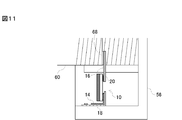
 12e …RFICチップ(無線通信用集積回路)
 12h …第1入出力端子
 12i …第2入出力端子
 12j …給電回路
 14 …励振導体
 16 …接続用導体
 18,20 …フレキシブル基材
 30 …高圧ガスバルブ(物品)
 36 …スピンドル(金属体)
 38 …弁(金属体)
 50 …測定器(物品)
 60 …スピンドル(金属体)
 64 …グランド電極(金属体)
10 ... RFID tag (wireless communication tag)
12e ... RFIC chip (integrated circuit for wireless communication)
12h ... 1st input / output terminal 12i ... 2nd input / output terminal 12j ... Feeding circuit 14 ... Excitation conductor 16 ... Connection conductor 18, 20 ... Flexible base material 30 ... High pressure gas valve (article)
36 ... Spindle (metal body)
38 ... Valve (metal body)
50 ... Measuring instrument (article)
60 ... Spindle (metal body)
64: Ground electrode (metal body)

Claims (9)

  1.  無線通信タグが付属する物品であって、
     前記無線通信タグは、
     第1入出力端子および第2入出力端子を有する無線通信用集積回路、
     前記第1入出力端子に接続された一端と開放された他端とを有する励振導体、および
     前記第2入出力端子に接続された一端と開放された他端とを有する接続用導体を備え、
     前記物品は一端が前記接続用導体の前記開放された他端に接続されかつ他端が開放された金属体を備える、無線通信タグ付き物品。
    An article with a wireless communication tag,
    The wireless communication tag is
    An integrated circuit for wireless communication having a first input / output terminal and a second input / output terminal;
    An excitation conductor having one end connected to the first input / output terminal and the other open end; and a connecting conductor having one end connected to the second input / output terminal and the other open end;
    An article with a wireless communication tag, comprising: a metal body having one end connected to the other open end of the connection conductor and the other end open.
  2.  前記第1入出力端子から前記励振導体の前記他端までの電気長は1/2波長未満である、請求項1記載の無線通信タグ付き物品。 The article with a wireless communication tag according to claim 1, wherein an electrical length from the first input / output terminal to the other end of the excitation conductor is less than ½ wavelength.
  3.  前記第1入出力端子から前記励振導体の前記他端までの電気長はほぼ1/4波長である、請求項2記載の無線通信タグ付き物品。 The article with a wireless communication tag according to claim 2, wherein an electrical length from the first input / output terminal to the other end of the excitation conductor is approximately ¼ wavelength.
  4.  前記第2入出力端子から前記金属体の開放端までの電気長は1/2波長以上である、請求項1ないし3のいずれかに記載の無線通信タグ付き物品。 The article with a wireless communication tag according to any one of claims 1 to 3, wherein an electrical length from the second input / output terminal to the open end of the metal body is ½ wavelength or more.
  5.  前記無線通信タグは所定の共振周波数を有する給電回路をさらに備え、
     前記励振導体および前記接続用導体はそれぞれ前記給電回路を介して前記第1入出力端子および前記第2入出力端子に接続される、請求項1ないし4のいずれかに記載の無線通信タグ付き物品。
    The wireless communication tag further includes a power supply circuit having a predetermined resonance frequency,
    The article with a wireless communication tag according to any one of claims 1 to 4, wherein the excitation conductor and the connection conductor are connected to the first input / output terminal and the second input / output terminal via the feeder circuit, respectively. .
  6.  前記励振導体および前記接続用導体の各々はフレキシブル基材に形成される、請求項1ないし5のいずれかに記載の無線通信タグ付き物品。 The article with a wireless communication tag according to any one of claims 1 to 5, wherein each of the excitation conductor and the connection conductor is formed on a flexible base material.
  7.  前記金属体は柱状体を含み、前記無線通信タグは前記柱状体の一方端面に接続されている、請求項1ないし6のいずれかに記載の無線通信タグ付き物品。 The article with a wireless communication tag according to any one of claims 1 to 6, wherein the metal body includes a columnar body, and the wireless communication tag is connected to one end face of the columnar body.
  8.  前記柱状体は円柱状のスピンドルである、請求項7記載の無線通信タグ付き物品。 The article with a wireless communication tag according to claim 7, wherein the columnar body is a cylindrical spindle.
  9.  第1入出力端子および第2入出力端子を有する無線通信用集積回路、
     前記第1入出力端子に接続された一端と開放された他端とを有する励振導体、および
     前記第2入出力端子に接続された一端と開放された他端とを有する接続用導体を備える無線通信タグであって、
     前記接続用導体の前記開放された他端は物品の少なくとも一部をなしかつ他端が開放された金属体の一端に接続される、無線通信タグ。
    An integrated circuit for wireless communication having a first input / output terminal and a second input / output terminal;
    A radio comprising an excitation conductor having one end connected to the first input / output terminal and an open other end, and a connection conductor having one end connected to the second input / output terminal and the other open end A communication tag,
    The wireless communication tag, wherein the opened other end of the connection conductor constitutes at least a part of an article and is connected to one end of a metal body having the other end opened.
PCT/JP2015/050683 2014-01-23 2015-01-13 Article with radio communication tag and radio communication tag WO2015111466A1 (en)

Priority Applications (3)

Application Number Priority Date Filing Date Title
JP2015558804A JP6007448B2 (en) 2014-01-23 2015-01-13 Article with wireless communication tag and wireless communication tag
DE112015000479.3T DE112015000479T5 (en) 2014-01-23 2015-01-13 Article with wireless communication identifier and wireless communication identifier
CN201590000247.1U CN206585073U (en) 2014-01-23 2015-01-13 Article and wireless communication tag with wireless communication tag

Applications Claiming Priority (4)

Application Number Priority Date Filing Date Title
JP2014009962 2014-01-23
JP2014-009962 2014-01-23
JP2014-049732 2014-03-13
JP2014049732 2014-03-13

Publications (1)

Publication Number Publication Date
WO2015111466A1 true WO2015111466A1 (en) 2015-07-30

Family

ID=53681273

Family Applications (1)

Application Number Title Priority Date Filing Date
PCT/JP2015/050683 WO2015111466A1 (en) 2014-01-23 2015-01-13 Article with radio communication tag and radio communication tag

Country Status (4)

Country Link
JP (2) JP6007448B2 (en)
CN (2) CN209712910U (en)
DE (1) DE112015000479T5 (en)
WO (1) WO2015111466A1 (en)

Cited By (1)

* Cited by examiner, † Cited by third party
Publication number Priority date Publication date Assignee Title
DE212017000183U1 (en) 2016-07-14 2019-02-14 Murata Manufacturing Co., Ltd. Attention label for retail items and retail items to which it is attached

Families Citing this family (1)

* Cited by examiner, † Cited by third party
Publication number Priority date Publication date Assignee Title
WO2019039484A1 (en) * 2017-08-24 2019-02-28 株式会社村田製作所 Package with rfid tag

Citations (3)

* Cited by examiner, † Cited by third party
Publication number Priority date Publication date Assignee Title
WO2009008296A1 (en) * 2007-07-09 2009-01-15 Murata Manufacturing Co., Ltd. Wireless ic device
JP2013055457A (en) * 2011-09-02 2013-03-21 Toppan Printing Co Ltd Non-contact ic label
JP2013258779A (en) * 2011-02-28 2013-12-26 Murata Mfg Co Ltd Wireless communication device

Family Cites Families (8)

* Cited by examiner, † Cited by third party
Publication number Priority date Publication date Assignee Title
JP2737942B2 (en) * 1988-08-22 1998-04-08 ソニー株式会社 Receiving machine
JPH10256819A (en) * 1997-03-12 1998-09-25 Toshiba Corp Radio equipment and radio system
JP4086991B2 (en) * 1999-01-21 2008-05-14 株式会社日立国際電気 Small antenna for radio
EP2166616B1 (en) * 2007-07-18 2013-11-27 Murata Manufacturing Co. Ltd. Wireless ic device
JP5291571B2 (en) * 2009-08-18 2013-09-18 トッパン・フォームズ株式会社 Non-contact communication part built-in metal housing
JP5286195B2 (en) * 2009-08-18 2013-09-11 トッパン・フォームズ株式会社 Non-contact communication part built-in metal housing
JP5355472B2 (en) * 2009-12-10 2013-11-27 ニッタ株式会社 Information storage medium, managed article and management system
JP5834987B2 (en) * 2012-02-15 2015-12-24 株式会社村田製作所 ANTENNA DEVICE AND WIRELESS COMMUNICATION DEVICE

Patent Citations (3)

* Cited by examiner, † Cited by third party
Publication number Priority date Publication date Assignee Title
WO2009008296A1 (en) * 2007-07-09 2009-01-15 Murata Manufacturing Co., Ltd. Wireless ic device
JP2013258779A (en) * 2011-02-28 2013-12-26 Murata Mfg Co Ltd Wireless communication device
JP2013055457A (en) * 2011-09-02 2013-03-21 Toppan Printing Co Ltd Non-contact ic label

Cited By (3)

* Cited by examiner, † Cited by third party
Publication number Priority date Publication date Assignee Title
DE212017000183U1 (en) 2016-07-14 2019-02-14 Murata Manufacturing Co., Ltd. Attention label for retail items and retail items to which it is attached
DE112017003598T5 (en) 2016-07-14 2019-05-02 Murata Manufacturing Co., Ltd. ATTENTION TO LABEL FOR RETAIL GOODS AND RETAIL ITEMS TO WHICH IT IS ATTACHED
US11087197B2 (en) 2016-07-14 2021-08-10 Murata Manufacturing Co., Ltd. Attention tag for retail article and retail article having same attached thereto

Also Published As

Publication number Publication date
CN206585073U (en) 2017-10-24
JP6337931B2 (en) 2018-06-06
DE112015000479T5 (en) 2016-11-10
CN209712910U (en) 2019-12-03
JP2016226047A (en) 2016-12-28
JPWO2015111466A1 (en) 2017-03-23
JP6007448B2 (en) 2016-10-12

Similar Documents

Publication Publication Date Title
JP4525859B2 (en) Wireless IC device
US8360325B2 (en) Wireless IC device, electronic apparatus, and method for adjusting resonant frequency of wireless IC device
JP5808374B2 (en) Articles with wireless communication devices
JP5703977B2 (en) Metal articles with wireless communication devices
JP5505581B1 (en) Antenna device and communication terminal device
JP2011109552A (en) Radio tag
US10387764B2 (en) RFID tag, article including the same, and RFID tag manufacturing method
JP2012253699A (en) Wireless communication device, its manufacturing method, and metal article with wireless communication device
JP6452477B2 (en) Antenna and communication device using the same
JP2013247526A (en) Antenna device
JP6337931B2 (en) Article with wireless communication tag and wireless communication tag
JPWO2020110930A1 (en) RFID tag
US9728851B2 (en) Mobile communication device
JP6658889B2 (en) Antenna and wireless module
JP5943229B2 (en) Articles with wireless communication tags
WO2013183574A1 (en) Antenna and wireless communication apparatus
JP7244812B1 (en) power receiving antenna
KR102209674B1 (en) Electronic device having antenna
US9652649B2 (en) Chip-type antenna device and chip structure
WO2023074699A1 (en) Power-receiving antenna
TWI298139B (en) Antenna and tag for rfid using the antenna
WO2018016339A1 (en) Multiband antenna and electronic device
KR20210023785A (en) Electronic device having antenna
WO2013168690A1 (en) Antenna device
JP4433097B2 (en) Wireless IC device

Legal Events

Date Code Title Description
121 Ep: the epo has been informed by wipo that ep was designated in this application

Ref document number: 15740456

Country of ref document: EP

Kind code of ref document: A1

ENP Entry into the national phase

Ref document number: 2015558804

Country of ref document: JP

Kind code of ref document: A

WWE Wipo information: entry into national phase

Ref document number: 112015000479

Country of ref document: DE

122 Ep: pct application non-entry in european phase

Ref document number: 15740456

Country of ref document: EP

Kind code of ref document: A1