WO2015107855A1 - Normal temperature bonding device - Google Patents
Normal temperature bonding device Download PDFInfo
- Publication number
- WO2015107855A1 WO2015107855A1 PCT/JP2014/084495 JP2014084495W WO2015107855A1 WO 2015107855 A1 WO2015107855 A1 WO 2015107855A1 JP 2014084495 W JP2014084495 W JP 2014084495W WO 2015107855 A1 WO2015107855 A1 WO 2015107855A1
- Authority
- WO
- WIPO (PCT)
- Prior art keywords
- carriage
- wafer
- lower wafer
- room temperature
- stage
- Prior art date
Links
Images


Classifications
-
- H—ELECTRICITY
- H01—ELECTRIC ELEMENTS
- H01L—SEMICONDUCTOR DEVICES NOT COVERED BY CLASS H10
- H01L21/00—Processes or apparatus adapted for the manufacture or treatment of semiconductor or solid state devices or of parts thereof
- H01L21/67—Apparatus specially adapted for handling semiconductor or electric solid state devices during manufacture or treatment thereof; Apparatus specially adapted for handling wafers during manufacture or treatment of semiconductor or electric solid state devices or components ; Apparatus not specifically provided for elsewhere
- H01L21/683—Apparatus specially adapted for handling semiconductor or electric solid state devices during manufacture or treatment thereof; Apparatus specially adapted for handling wafers during manufacture or treatment of semiconductor or electric solid state devices or components ; Apparatus not specifically provided for elsewhere for supporting or gripping
- H01L21/687—Apparatus specially adapted for handling semiconductor or electric solid state devices during manufacture or treatment thereof; Apparatus specially adapted for handling wafers during manufacture or treatment of semiconductor or electric solid state devices or components ; Apparatus not specifically provided for elsewhere for supporting or gripping using mechanical means, e.g. chucks, clamps or pinches
- H01L21/68714—Apparatus specially adapted for handling semiconductor or electric solid state devices during manufacture or treatment thereof; Apparatus specially adapted for handling wafers during manufacture or treatment of semiconductor or electric solid state devices or components ; Apparatus not specifically provided for elsewhere for supporting or gripping using mechanical means, e.g. chucks, clamps or pinches the wafers being placed on a susceptor, stage or support
- H01L21/68785—Apparatus specially adapted for handling semiconductor or electric solid state devices during manufacture or treatment thereof; Apparatus specially adapted for handling wafers during manufacture or treatment of semiconductor or electric solid state devices or components ; Apparatus not specifically provided for elsewhere for supporting or gripping using mechanical means, e.g. chucks, clamps or pinches the wafers being placed on a susceptor, stage or support characterised by the mechanical construction of the susceptor, stage or support
-
- H—ELECTRICITY
- H01—ELECTRIC ELEMENTS
- H01L—SEMICONDUCTOR DEVICES NOT COVERED BY CLASS H10
- H01L21/00—Processes or apparatus adapted for the manufacture or treatment of semiconductor or solid state devices or of parts thereof
- H01L21/67—Apparatus specially adapted for handling semiconductor or electric solid state devices during manufacture or treatment thereof; Apparatus specially adapted for handling wafers during manufacture or treatment of semiconductor or electric solid state devices or components ; Apparatus not specifically provided for elsewhere
- H01L21/67005—Apparatus not specifically provided for elsewhere
- H01L21/67011—Apparatus for manufacture or treatment
- H01L21/67092—Apparatus for mechanical treatment
-
- B—PERFORMING OPERATIONS; TRANSPORTING
- B32—LAYERED PRODUCTS
- B32B—LAYERED PRODUCTS, i.e. PRODUCTS BUILT-UP OF STRATA OF FLAT OR NON-FLAT, e.g. CELLULAR OR HONEYCOMB, FORM
- B32B37/00—Methods or apparatus for laminating, e.g. by curing or by ultrasonic bonding
- B32B37/0046—Methods or apparatus for laminating, e.g. by curing or by ultrasonic bonding characterised by constructional aspects of the apparatus
-
- H—ELECTRICITY
- H01—ELECTRIC ELEMENTS
- H01L—SEMICONDUCTOR DEVICES NOT COVERED BY CLASS H10
- H01L21/00—Processes or apparatus adapted for the manufacture or treatment of semiconductor or solid state devices or of parts thereof
- H01L21/67—Apparatus specially adapted for handling semiconductor or electric solid state devices during manufacture or treatment thereof; Apparatus specially adapted for handling wafers during manufacture or treatment of semiconductor or electric solid state devices or components ; Apparatus not specifically provided for elsewhere
- H01L21/68—Apparatus specially adapted for handling semiconductor or electric solid state devices during manufacture or treatment thereof; Apparatus specially adapted for handling wafers during manufacture or treatment of semiconductor or electric solid state devices or components ; Apparatus not specifically provided for elsewhere for positioning, orientation or alignment
-
- B—PERFORMING OPERATIONS; TRANSPORTING
- B32—LAYERED PRODUCTS
- B32B—LAYERED PRODUCTS, i.e. PRODUCTS BUILT-UP OF STRATA OF FLAT OR NON-FLAT, e.g. CELLULAR OR HONEYCOMB, FORM
- B32B2313/00—Elements other than metals
-
- B—PERFORMING OPERATIONS; TRANSPORTING
- B32—LAYERED PRODUCTS
- B32B—LAYERED PRODUCTS, i.e. PRODUCTS BUILT-UP OF STRATA OF FLAT OR NON-FLAT, e.g. CELLULAR OR HONEYCOMB, FORM
- B32B2315/00—Other materials containing non-metallic inorganic compounds not provided for in groups B32B2311/00 - B32B2313/04
- B32B2315/08—Glass
Definitions
- the present invention relates to a room temperature bonding apparatus.
- Room temperature bonding is known as a technique for bonding two wafers (substrates).
- the room temperature bonding is a technique in which the surfaces of two wafers to be bonded are activated in a vacuum atmosphere, and the two wafers are bonded by bringing the activated wafer surfaces into contact with each other.
- a method for activating the wafer surface for example, a method using an ion beam and a method using a neutral atom beam are known.
- Patent Document 1 Japanese Patent No. 4822577
- Patent Document 2 Japanese Patent No. 4669766
- Patent Document 5 discloses a technique for increasing the load resistance of the stage mechanism.
- a carriage for holding a wafer is connected to a positioning stage by elastic guidance.
- a carriage support is provided. When no load is applied to the carriage, the carriage is supported so as not to contact the carriage support.
- the elastic guide is elastically deformed, the carriage comes into contact with the carriage support base, and the load is distributed to the carriage support base. Thereby, the load which acts on the positioning stage is reduced.
- Patent Document 6 discloses a room temperature bonding apparatus in which an angle adjustment mechanism for adjusting the orientation of a sample stage is provided on the upper stage.
- an object of the present invention is to provide a room temperature bonding apparatus having a stage mechanism that satisfies the requirements of precise alignment of wafers and large load resistance while having a large stroke.
- a room temperature bonding apparatus includes a bonding chamber, an upper stage mechanism that supports the upper wafer so as to be movable in the vertical direction inside the bonding chamber, and the lower wafer within the horizontal plane within the bonding chamber. And a lower stage mechanism that is movably supported.
- the lower stage mechanism includes a carriage having a lower wafer holding unit for holding the lower wafer, an elastic guide connected to the carriage to support the carriage, a positioning stage for coarsely moving the lower wafer holding unit, and a lower side
- a fine movement mechanism for finely moving the wafer holding unit and a carriage support base are included.
- the elastic guide supports the carriage so that the carriage does not contact the carriage support when no load is applied to the carriage from the upper stage mechanism, and the upper stage mechanism makes the upper wafer contact the lower wafer and move up and down the carriage.
- the carriage is elastically deformed so as to contact the carriage support.
- the positioning stage coarsely moves the lower wafer holder by driving the elastic guide, and the fine movement mechanism is incorporated in the carriage.
- the carriage includes a carriage plate to which elastic guides are joined, the lower wafer holding portion is located above the carriage plate, and the fine movement mechanism is a frame provided on the carriage plate; And a drive mechanism connected to the frame for driving the lower wafer holder.
- the elastic guide is elastically deformed so that the carriage plate comes into contact with the carriage support.
- the frame may be provided with a support mechanism for supporting the lower wafer holding portion so as to be movable in the vertical direction.
- the support mechanism supports the lower wafer holder so that the lower wafer holder does not contact the carriage plate when no load is applied from the upper stage mechanism to the lower wafer holder.
- the lower wafer holder may be elastically deformed so as to come into contact with the carriage plate.
- the fine movement mechanism may include a table and a drive mechanism that drives the table, and the elastic guide may connect the lower wafer holding unit to the table.
- the positioning stage coarsely moves the lower wafer holding unit by driving the entire fine movement mechanism, and the fine movement mechanism finely moves the lower wafer holding unit by driving the table by the driving mechanism.
- the upper stage mechanism may include an upper wafer holding part that holds the upper wafer and an angle adjustment mechanism that adjusts the direction of the upper wafer holding part.
- the upper stage mechanism includes an elevating rod that moves up and down.
- the angle adjusting mechanism includes a ball flange fixed to the upper wafer holding unit, a ball seat fixed to the elevating rod, and a ball seat, and the ball flange is clamped to connect the ball flange to the ball seat. It preferably includes a fixed flange.
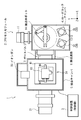
- FIG. 1 is a cross-sectional view schematically showing a configuration of a room temperature bonding apparatus 1 according to the first embodiment.
- an XYZ orthogonal coordinate system is used as necessary.
- the Z axis is defined in the vertical direction (vertical direction)
- the X axis is defined in a specific direction in a plane parallel to the horizontal plane
- the Y axis is defined in a direction perpendicular to the X axis and the Z axis.
- the room temperature bonding apparatus 1 includes a process module 2 that performs room temperature bonding and a control device (control panel) 3 that controls the process module 2.
- the process module 2 includes a load lock chamber 4 and a bonding chamber 5.
- the load lock chamber 4 is a chamber used for transferring a wafer between the external environment and the bonding chamber 5, and the bonding chamber 5 is a chamber in which the wafer is actually bonded.
- the process module 2 further includes a transfer passage 6 and a gate valve 7.
- the conveyance path 6 is interposed between the load lock chamber 4 and the bonding chamber 5, and connects the internal space of the bonding chamber 5 and the internal space of the load lock chamber 4.
- the gate valve 7 closes the transport passage 6 or opens the transport passage 6 under the control of the control device 3. That is, the gate valve 7 has a function of communicating or separating the internal space of the load lock chamber 4 with the internal space of the bonding chamber 5.
- the load lock chamber 4 includes a lid (not shown) and a vacuum exhaust device 11.
- the lid is operated by a user to close an opening (not shown) connecting the external environment and the inside of the load lock chamber 4 or open the opening.
- the vacuum exhaust device 11 exhausts gas from the inside of the load lock chamber 4 under the control of the control device 3.
- the load lock chamber 4 further accommodates cartridge bases 12 and 13 and a transfer robot 14 inside.
- Cartridges 31 and 32 holding wafers to be bonded are mounted on the cartridge bases 12 and 13, respectively.
- the cartridge 31 is a cartridge that holds a wafer positioned on the upper side (hereinafter also referred to as the upper wafer 33) when the wafers are bonded
- the cartridge 32 is a wafer positioned on the lower side (hereinafter referred to as the upper wafer 33).
- the transfer robot 14 transfers the cartridges 31 and 32 arranged on the cartridge bases 12 and 13 through the transfer path 6 to the inside of the bonding chamber 5 or the bonding chamber 5. Are transported to cartridge bases 12 and 13.
- the bonding chamber 5 includes a vacuum exhaust device 21.
- the vacuum exhaust device 21 exhausts gas from the inside of the bonding chamber 5 under the control of the control device 3.
- FIG. 2 is a cross-sectional view schematically showing the structure of the bonding chamber 5.
- the bonding chamber 5 further includes an ion gun 22, an upper stage mechanism 23, and a lower stage mechanism 24.
- the ion gun 22 emits an ion beam 22a used for activating the surface of the wafer. Irradiation with the ion beam 22 a activates the surfaces of the upper wafer 33 supported by the upper stage mechanism 23 and the lower wafer 34 supported by the lower stage mechanism 24.
- one ion gun 22 is used for activating the surface of the wafer, but a plurality of ion guns 22 may be used.
- other activating means for example, a neutral atom beam source
- the upper stage mechanism 23 is a mechanism for aligning the upper wafer 33, and includes an electrostatic chuck 25 and a pressure contact mechanism 26.
- the electrostatic chuck 25 functions as an upper wafer holding unit that holds the upper wafer 33.
- the electrostatic chuck 25 includes a dielectric layer, and has a flat surface substantially perpendicular to the vertical direction (Z-axis direction) at the lower end of the dielectric layer.
- the electrostatic chuck 25 further includes an internal electrode disposed inside the dielectric layer. The electrostatic chuck 25 applies a predetermined applied voltage to the internal electrode under the control of the control device 3 and holds the upper wafer 33 disposed in the vicinity of the flat surface of the dielectric layer by electrostatic force.
- the pressure contact mechanism 26 raises and lowers the electrostatic chuck 25 in the vertical direction (Z-axis direction) under the control of the control device 3. In one embodiment, the pressure contact mechanism 26 aligns the electrostatic chuck 25 at a desired position under the control of the control device 3. The pressure contact mechanism 26 further measures the position of the electrostatic chuck 25 (that is, the position of the upper wafer 33) under the control of the control device 3, and outputs data indicating the position to the control device 3. The pressure contact mechanism 26 further measures a load applied to the upper wafer 33 held by the electrostatic chuck 25 under the control of the control device 3, and outputs data indicating the load to the control device 3.
- the lower stage mechanism 24 is a mechanism for aligning the lower wafer 34, holds the cartridge 32 placed thereon, and thereby the lower wafer 34 held on the cartridge 32. Hold. Details of the lower stage mechanism 24 will be described later.
- the bonding chamber 5 further includes an alignment mechanism 27.
- the alignment mechanism 27 captures an image near the alignment mark provided on the surface of the upper wafer 33 held by the upper stage mechanism 23 and the lower wafer 34 placed on the lower stage mechanism 24.
- the captured image is sent to the control device 3 to be subjected to image processing, whereby the positional deviation in the XY plane and the positional deviation in the XY plane between the upper wafer 33 and the lower wafer 34 are detected. To detect. Details of the alignment mechanism 27 will be described later.
- the positional and orientation shift between the upper wafer 33 and the lower wafer 34 obtained by using the alignment mechanism 27 is used for controlling the lower stage mechanism 24.
- FIG. 3 is a block diagram schematically showing the configuration of the control device 3 in the present embodiment.
- the control device 3 is an information processing device exemplified by a computer, and includes a CPU (Central Processing Unit) 91, a memory 92, an input device 93, an output device 94, an interface 95, an external storage device 96, and a drive. 97.
- the CPU 91, the memory 92, the input device 93, the output device 94, the interface 95, the external storage device 96, and the drive 97 are connected to be communicable with each other.
- the CPU 91 expands the computer program 96 a installed in the external storage device 96 in the memory 92.
- the CPU 91 further executes the expanded computer program 96a to realize information processing of the computer program 96a while controlling hardware such as the input device 93, the output device 94, and the external storage device 96 as necessary. .
- the external storage device 96 records the computer program 96a and also records information used by the CPU 91 and information to be generated.
- a recording medium 98 on which the computer program 96a is recorded may be used.
- the computer program 96 a is read by the drive 97, and the read computer program 96 a is written to the external storage device 96.
- the input device 93 outputs information generated by being operated by the user to the CPU 91 and the external storage device 96.
- the output device 94 outputs information generated by the CPU 91 and information in the external storage device 96 so that the user can recognize it.
- the interface 95 is used for communication between each device of the process module 2 and the control device 3. Specifically, the interface 95 includes the gate valve 7, the transfer robot 14, the vacuum exhaust devices 11 and 21, the ion gun 22, the upper stage mechanism 23 (that is, the electrostatic chuck 25 and the pressure contact mechanism 26), and the lower stage mechanism 24. Control signals to be controlled are transmitted, and signals transmitted from these devices are received.
- the computer program 96a installed in the control device 3 includes a program code group for causing the control device 3 to realize a desired function.
- the program code group provides a function of controlling the process module 2 with respect to the transfer, installation and removal of the wafers 33 and 34. In this function, mainly control of the vacuum exhaust device 11 of the load lock chamber 4, control of opening / closing of the gate valve 7, control of transport of the cartridges 31 and 32 by the transport robot 14, control of the electrostatic chuck 25, and press-contact mechanism 26 Control is performed.
- the program code group provides a function of controlling the process module 2 with respect to the activation of the wafers 33 and 34.
- control of the vacuum exhaust device 21 of the bonding chamber 5, control of the pressure contact mechanism 26, and control of the ion gun 22 are mainly performed.
- the program code group provides a function of controlling the process module 2 with respect to the bonding of the wafers 33 and 34. In this function, control of the electrostatic chuck 25, control of the pressure contact mechanism 26, and control of the lower stage mechanism 24 are mainly performed.
- the lower stage mechanism 24 is configured to satisfy both requirements of precise alignment of the wafer and a large load resistance while being able to provide a sufficiently large stroke.
- the configuration of the lower stage mechanism 24 in the present embodiment will be described in detail.
- FIG. 4A is a schematic diagram schematically showing the configuration of the lower stage mechanism 24.
- the lower stage mechanism 24 includes a positioning stage 41, a carriage support base 42, a carriage 43, and an elastic guide 44.
- the positioning stage 41 and the carriage support 42 are supported by the bottom plate 5 a of the bonding chamber 5.
- the positioning stage 41 functions as a coarse movement stage that coarsely moves the lower wafer 34 with a large stroke.
- the carriage support base 42 has a smooth support surface 42a at its upper end.
- the support surface 42a is perpendicular to the vertical direction (Z-axis direction).
- the carriage 43 holds the cartridge 32 (and the lower wafer 34 placed on the cartridge 32) placed thereon.
- a function of a fine movement stage for finely moving the lower wafer 34 with a small stroke is incorporated in the carriage 43.
- the elastic guide 44 is formed of an elastic body and is joined to the side surface of the carriage 43.
- the carriage 43 is connected to the positioning stage 41 by an elastic guide 44.
- the elastic guide 44 supports the carriage 43 so that the lower surface 43 a of the carriage 43 does not come into contact with the support surface 42 a of the carriage support base 42 when no load is applied to the carriage 43.
- a gap of about 100 ⁇ m is provided between the lower surface 43 a of the carriage 43 and the support surface 42 a of the carriage support 42.
- the elastic guide 44 is elastically deformed so that the lower surface 43a of the carriage 43 contacts the support surface 42a of the carriage support base 42.
- the positioning stage 41 drives the elastic guide 44 and the carriage 43 connected to the elastic guide 44. More specifically, the positioning stage 41 moves in the X-axis direction and the Y-axis direction, and in the ⁇ -angle direction. It is configured to rotate.
- the positioning stage 41 incorporates a moving / rotating mechanism (not shown) using, for example, a ball screw, a linear guide, and a motor, and the positioning stage 41 functions as a coarse movement stage. If necessary, the carriage 43 is moved and / or rotated by the positioning stage 41, so that the cartridge 32 placed on the carriage 43 (and the lower wafer 34 placed on the cartridge 32) is moved and / or moved. It is rotated.
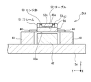
- FIG. 4B is a schematic diagram illustrating a structure of a portion related to the alignment mechanism 27 of the lower stage mechanism 24.
- the alignment mechanism 27 includes an infrared illumination 101 that generates infrared rays, a lens 102 that changes the direction of the infrared rays to a vertical direction, and a camera 103. Further, a transparent portion 104 is formed on the carriage support 42, and a transparent portion 105 is formed on the carriage 43 (more precisely, on the stage 52 of the carriage 43 as will be described later).
- the transparent portions 104 and 105 are both made of a material that is transparent to the infrared rays that the infrared illumination 101 irradiates.
- the transparent portion 105 of the carriage 43 is disposed in the vicinity of the transparent portion 104 of the carriage support base 42.
- the alignment mechanism 27 uses a transparent portion 106 provided on the cartridge 32 placed on the carriage 43, an alignment mark 107 provided on the upper wafer 33, and an alignment mark 108 provided on the lower wafer 34.
- the position and orientation deviation between the upper wafer 33 and the lower wafer 34 is detected.
- the transparent portion 106 is formed of a material that is transparent to the infrared rays irradiated by the infrared illumination 101.
- the lens 102 changes the direction of the infrared rays generated by the infrared illumination 101 to the vertical direction, and makes the infrared rays enter the upper wafer 33 and the lower wafer 34 through the transparent portions 104, 105, and 106.
- insulating materials eg, glass
- semiconductors eg, silicon
- the lens 102 further enters the camera 103 with reflected light generated by reflecting the infrared rays by the upper wafer 33 and the lower wafer 34.
- the camera 103 captures the reflected light that has passed through the lens 102 and obtains images of parts of the upper wafer 33 and the lower wafer 34 (that is, images near the alignment marks 107 and 108).
- the obtained image is sent to the control device 3, and the control device 3 performs image processing on the image. By this image processing, the position and the deviation of the upper wafer 33 and the lower wafer 34 are detected.
- a cavity (or hole) for allowing infrared light to pass through may be provided instead of providing the transparent portion 104 on the carriage support base 42.
- a cavity (or hole) for allowing infrared light to pass through may be provided instead of providing the transparent portions 105 and 106 in the carriage 43 and the cartridge 32.
- a cavity (or hole) for allowing infrared rays to pass therethrough may be provided.
- the carriage support base 42 may be provided with the transparent portion 104, and the carriage 43 and the cartridge 32 may be provided with a cavity for allowing infrared light to pass through.
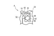
- FIG. 5A is a plan view showing the configuration of the carriage 43.
- the carriage 43 includes a frame 51 and a table 52.
- the frame 51 is connected to the positioning stage 41 by the elastic guide 44 described above.
- the table 52 is used as a lower wafer holding unit for holding the cartridge 32 (and the lower wafer 34 placed on the cartridge 32) placed thereon.
- the table 52 is formed with the transparent portion 105 described above.
- the table 52 of the carriage 43 may be provided with a cavity (or hole) for allowing infrared light to pass instead of the transparent portion 105.
- the table 52 is disposed so as to be surrounded by the frame 51, and is movably supported by the frame 51 by a plurality of hinge portions 53. In the present embodiment, four corners of the table 52 are connected to the frame 51 by four hinge portions 53.
- FIG. 5B is a plan view showing the configuration of the hinge portion 53.
- Each hinge portion 53 has small piece members 61 and 62.
- the small piece member 61 is connected to the table 52 by the narrowed portion 63 and is connected to the small piece member 62 by the narrowed portion 64.
- the small piece member 62 is connected to the frame 51 by a narrow portion 65.
- FIG. 5C is a perspective view showing the structure of the narrow portion 63.
- the narrow part 63 is configured as a narrow structure and can be bent.
- the narrow portions 64 and 65 are configured as a narrow structure and can be bent.
- the hinge 53 having such a structure connects the table 52 to the frame 51 so that the table 52 can be moved in the X-axis direction and the Y-axis direction and can be rotated in the ⁇ -angle direction.
- the ⁇ angle direction is an angle direction in the XY plane.
- the carriage 43 further includes three drive mechanisms 54 1 to 54 3 for driving the table 52.
- Drive mechanism 54 1, 54 2 drives the table 52 in the X-axis direction
- the driving mechanism 543 drives the table 52 in the Y-axis direction.
- the three drive mechanisms 54 1 to 54 3 are used as fine movement mechanisms for finely moving the table 52.
- the drive mechanism 54 1 includes a piezoelectric element 55 1 and a connecting portion 56 1 .
- the piezoelectric element 55 1 has one end connected to the frame 51, are connected to the connecting portion 56 1 and the other end.
- the piezoelectric element 55 1, the connecting portion 56 1 is moved in the X-axis direction in accordance with the supplied voltage to it.
- Connecting portion 56 1 has its one end connected to the piezoelectric element 55 1, and the other end is connected to the table 52.
- the connecting portions 56 1, two narrow portion 57 is provided, which is bendable in the narrow portion 57.
- Drive mechanism 542 also, the driving mechanism 54 1 is configured similarly to, and a piezoelectric element 55 2 and the connecting portion 56 2.
- the piezoelectric element 55 2 has one end connected to the frame 51, are connected to the connecting portion 56 2 and the other end.
- the piezoelectric element 55 2, the coupling portion 56 2 is moved in the X-axis direction in accordance with the supplied voltage to it.
- Connecting portion 56 2 has its one end connected to the piezoelectric element 55 2, and the other end is connected to the table 52.
- Connecting portion 56 2 the two are narrow portion is provided, it is bendable in said narrow portion.
- Such a structure table 52 by the drive mechanism 543 even when it is driven in the Y-axis direction can be absorbed by the curvature of the narrow portion of the displacement of the coupling portion 56 2 in the Y-axis direction of the table 52.
- the drive mechanism 543 also, except that the direction for driving the table 52 are different, it has the same configuration as the drive mechanism 54 1, 54 2.
- the drive mechanism 543 is provided with a connecting portion 56 3 and the piezoelectric element 55 3.
- the piezoelectric element 55 3 has one end connected to the frame 51, are connected to the connecting portion 56 3 and the other end.
- the piezoelectric element 55 3, a connecting portion 56 3 is moved in the Y-axis direction according to the voltage supplied thereto.
- Connecting portion 56 3 has its one end connected to the piezoelectric element 55 3, and the other end is connected to the table 52.
- Connecting portion 56 3, two have narrow portion is provided, it is bendable in said narrow portion.
- the carriage 43 having such a configuration functions as a fine stage that can move the table 52 in the X-axis direction and the Y-axis direction and that can rotate in the ⁇ -angle direction.
- the drive mechanism 54 1, 54 2 of the piezoelectric elements 55 1, 55 2 voltages such as a piezoelectric element 55 1, 55 2 have the same displacement is supplied. Accordingly, the table 52 can be moved to the desired position in the X-axis direction by appropriately adjusting the voltage supplied to the piezoelectric elements 55 1 and 55 2 .
- the drive mechanism 54 1, 54 2 of the piezoelectric elements 55 1, 55 2 when moving the Y-axis direction on the table 52, the drive mechanism 54 1, 54 2 of the piezoelectric elements 55 1, 55 2, voltages such as a piezoelectric element 55 1, 55 2 have the same displacement are provided . Accordingly, the table 52 can be moved to the desired position in the X-axis direction by appropriately adjusting the voltage supplied to the piezoelectric elements 55 1 and 55 2 . Furthermore, theta when rotating the table 52 in angular direction, the drive mechanism 54 1, 54 piezoelectric element 55 1 of 2, 55 2, voltages such as a piezoelectric element 55 1, 55 2 is different from the displacement is supplied. By appropriately adjusting the voltage supplied to the piezoelectric elements 55 1 and 55 2 , the table 52 can be rotated to a desired angle in the ⁇ angle direction.
- the carriage 43 for using a piezoelectric element 55 1, 55 2, 55 3 the movement of the table 52, the table 52 is moved at a high precision, or can be rotated. In other words, the carriage 43 can align the lower wafer 34 held by the cartridge 32 placed on the table 52 with high accuracy.
- the positioning stage 41 operates as a coarse movement stage mechanism, and the carriage 43 operates as a fine movement stage mechanism. That is, the positioning stage 41 operates as a stage mechanism that has a large stroke but a low accuracy compared to the carriage 43.
- the carriage 43 operates as a stage mechanism with a smaller stroke but higher accuracy than the positioning stage 41.
- the lower wafer 34 When the lower wafer 34 needs to be moved or rotated in at least one of the X axis direction, the Y axis direction, and the ⁇ angle direction with a small displacement, the lower wafer 34 is moved or rotated by the carriage 43. Is done. By such an operation, the lower stage mechanism 24 can realize a sufficiently large stroke and precise alignment of the wafer.
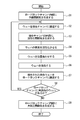
- FIG. 6 is a flowchart showing the room temperature bonding method in the present embodiment. This room temperature bonding method is performed using the room temperature bonding apparatus 1 described above.
- the lid of the load lock chamber 4 is closed, and a preliminary atmosphere is generated inside the load lock chamber 4 by the vacuum exhaust device 11 of the load lock chamber 4 (step S1).
- the preliminary atmosphere is an atmosphere of a degree of vacuum that allows the load lock chamber 4 and the joining chamber 5 to communicate with each other via the transfer passage 6 by opening the gate valve 7.
- one upper wafer 33 and one lower wafer 34 are transferred to the bonding chamber 5 (step S2). Specifically, first, the gate valve 7 is opened, and the transfer robot 14 moves the cartridge 31 on which the upper wafer 33 is placed from the cartridge base 12 of the load lock chamber 4 onto the table 52 of the carriage 43 of the bonding chamber 5. Be transported. Subsequently, the electrostatic chuck 25 is lowered by the pressure contact mechanism 26. The lowering of the electrostatic chuck 25 is stopped when the upper wafer 33 placed on the cartridge 31 comes into contact with the electrostatic chuck 25. Subsequently, the upper wafer 33 is held on the electrostatic chuck 25.
- the electrostatic chuck 25 is raised by the pressure contact mechanism 26 until it is positioned at a predetermined standby position. Subsequently, the cartridge 31 is transported from the carriage 43 to the cartridge base 12 by the transport robot 14. Thereafter, the transfer robot 14 transfers the cartridge 32 on which the lower wafer 34 is placed from the cartridge table 13 onto the table 52 of the carriage 43. Subsequently, the gate valve 7 is closed.
- step S3 an activation atmosphere is generated inside the bonding chamber 5 (step S3). More specifically, the degree of vacuum inside the bonding chamber 5 is adjusted to about 10 ⁇ 5 to 10 ⁇ 6 Pa by the control of the vacuum exhaust device 21.
- the surfaces of the upper wafer 33 and the lower wafer 34 are activated (step S4). Specifically, an ion beam 22 a is emitted from the ion gun 22, and the surfaces of the upper wafer 33 and the lower wafer 34 are irradiated with the ion beam 22 a. Thereby, the surfaces of the upper wafer 33 and the lower wafer 34 are etched. During irradiation with the ion beam 22a, the degree of vacuum inside the bonding chamber 5 is about 10 ⁇ 2 to 10 ⁇ 3 Pa.
- step S5 alignment of the upper wafer 33 and the lower wafer 34 is performed by the upper stage mechanism 23 and the lower stage mechanism 24 (step S5). Specifically, the electrostatic chuck 25 is lowered by the pressure contact mechanism 26 of the upper stage mechanism 23, and the electrostatic chuck 25 is disposed at a predetermined alignment position. At this time, the upper wafer 33 and the lower wafer 34 are separated by a predetermined alignment distance. Further, the lower wafer mechanism 34 is moved and / or rotated by the lower stage mechanism 24 to perform alignment with the upper wafer 33 in the horizontal plane.
- the alignment of the upper wafer 33 and the lower wafer 34 is performed according to the following procedure. First, using the alignment mechanism 27 provided in the bonding chamber 5, the displacement amount of the alignment marks 107 and 108 on the upper wafer 33 and the lower wafer 34 (deviation amount in the X-axis direction and deviation amount in the Y-axis direction). Then, a deviation amount in the direction (a deviation amount in the ⁇ angle direction) is calculated. The displacement amount of the position is calculated as a difference between the positions of the alignment marks 107 and 108, and the displacement amount of the direction is calculated as a difference between the angles of the alignment marks 107 and 108. When both the position of the alignment mark and the amount of misalignment are within the reference range determined for each, the alignment of the upper wafer 33 and the lower wafer 34 is completed.
- the lower stage mechanism 24 moves and moves the lower wafer 34 so as to eliminate this displacement amount. / Or rotate.
- the magnitude of the shift amount and direction of the deviation amount of the position of the alignment mark, and flutter lower wafer 34 by the positioning stage 41, the fine movement of the lower wafer 34 by the driving mechanism 54 1-54 3 the carriage 43 Is selectively performed.
- the carriage 43 is driven by the positioning stage 41, and the carriage 43 is moved and / or moved. Or rotated.
- both the shift amount and direction of deviation of the position of the alignment mark is less than a threshold value that is determined for each table 52 is driven by a drive mechanism 54 1-54 3 the carriage 43.
- the lower wafer 34 placed on the cartridge 32 held on the table 52 is driven so as to eliminate the displacement amount of the alignment mark and the displacement amount thereof.
- step S6 the upper wafer 33 and the lower wafer 34 are contacted, and the upper wafer 33 and the lower wafer 34 are bonded (step S6).
- the electrostatic chuck 25 is lowered by the pressure contact mechanism 26, and the surface of the upper wafer 33 is brought into contact with the surface of the lower wafer 34.
- the lowering of the electrostatic chuck 25 is stopped when the load applied to the electrostatic chuck 25 reaches a predetermined bonding load. That is, a bonding load is applied to the upper wafer 33 and the lower wafer 34.
- the upper wafer 33 and the lower wafer 34 are bonded to each other by applying a bonding load, and are formed into one bonded wafer. Application of the bonding load to the bonded wafer is continuously performed for a predetermined bonding time.
- a load is also applied to the table 52 of the carriage 43 in the vertically downward direction.
- the elastic guide 44 is elastically deformed, and the lower surface 43 a of the carriage 43 comes into contact with the support surface 42 a of the carriage support base 42.
- the load applied to the table 52 is mainly applied to the carriage support 42, and the load applied to the positioning stage 41 is reduced. This means that the load resistance of the lower stage mechanism 24 can be increased.
- the bonded wafer is transferred to the load lock chamber 4 (step S7). Specifically, after the bonded wafer is detached from the electrostatic chuck 25, the electrostatic chuck 25 is raised by the pressure contact mechanism 26. At this time, the bonded wafer is placed on the cartridge 32. Thereafter, when the gate valve 7 is opened, the transfer robot 14 transfers the cartridge 32 on which the bonded wafer is placed from the table 52 of the carriage 43 to the load lock chamber 4 and returns to the cartridge table 13.
- step S8 When the cartridge 31 on which the upper wafer 33 that has not yet been bonded and the cartridge 32 on which the lower wafer 34 that has not yet been bonded remain on the cartridge bases 12 and 13 (YES in step S8), The operations from step S2 to step S7 are executed again.
- step S8 when the bonding of all the upper wafers 33 and the lower wafers 34 has been completed (step S8, NO), the evacuation device 11 of the load lock chamber 4 is controlled, and the atmospheric pressure atmosphere is set inside the load lock chamber 4. Is generated (step S9).
- the user can open the lid of the load lock chamber 4 and take out the cartridge 32 on which the bonded wafer is placed and the cartridge 31 on which nothing is placed from the cartridge bases 12 and 13.
- the procedure for bonding the upper wafer 33 and the lower wafer 34 is completed.
- the above-described steps S1 to S9 are realized by executing the computer program 36a in the control device 3.
- the positioning stage 41 of the lower stage mechanism 24 operates as a coarse movement stage mechanism that coarsely moves the lower wafer 34, and the carriage 43 finely moves the lower wafer 34. Operates as a fine movement stage mechanism. By such an operation, the lower stage mechanism 24 can realize a sufficiently large stroke and precise alignment of the wafer.
- the elastic guide 44 that supports the carriage 43 is elastically deformed, and the lower surface 43a of the carriage 43 contacts the support surface 42a of the carriage support base 42. .
- the load is mainly applied to the carriage support base 42. Therefore, the load acting on the positioning stage 41 that functions as the coarse movement stage mechanism is reduced. According to such a structure, the load resistance of the lower stage mechanism 24 can be increased.
- FIG. 7 is a cross-sectional view schematically showing the configuration of the room temperature bonding apparatus 1 according to the second embodiment of the present invention, in particular, the configuration of the lower stage mechanism 24A.
- the configuration of the room temperature bonding apparatus 1 of the second embodiment is substantially the same as that of the room temperature bonding apparatus 1 of the first embodiment.
- the configuration of the lower stage mechanism 24A is different from the configuration of the lower stage mechanism 24 of the first embodiment.
- an alignment mechanism 27 may be incorporated in the lower stage 24A, but is not shown in FIG.
- the carriage 43A of the lower stage mechanism 24A includes a carriage plate 46 and a fine movement stage 47 mounted on the carriage plate 46.
- the carriage plate 46 is connected to the positioning stage 41 by an elastic guide 44.
- the positioning stage 41 functions as a coarse movement stage having a large stroke.
- the carriage plate 46 has a smooth upper surface and a smooth lower surface.
- the elastic guide 44 supports the carriage plate 46 so that the lower surface of the carriage plate 46 does not come into contact with the support surface 42a of the carriage support base 42 when no load is applied to the carriage 43A. At this time, a gap of about 100 ⁇ m is provided between the lower surface of the carriage plate 46 and the support surface 42 a of the carriage support base 42.
- the elastic guide 44 is elastically deformed so that the lower surface of the carriage plate 46 contacts the support surface 42a of the carriage support base 42.
- the fine movement stage 47 has the same configuration as the carriage 43 shown in FIGS. 5A to 5C (however, the frame 51 is not directly connected to the elastic guide 44).
- the fine movement stage 47 includes a frame 51 and a table 52.
- the table 52 is used as a lower wafer holding unit that holds the cartridge 32 (and the lower wafer 34 placed on the cartridge 32) placed thereon.
- the table 52 is disposed so as to be surrounded by the frame 51, and is movably supported by the frame 51 by four hinge portions 53.
- Fine movement stage 47 further includes three drive mechanisms 54 1 to 54 3 for driving table 52.
- Drive mechanism 54 1, 54 2 drives the table 52 in the X-axis direction
- the driving mechanism 543 drives the table 52 in the Y-axis direction.
- the frame 51 of the fine movement stage 47 and the lower surface of the table 52 are joined to the upper surface of the carriage plate 46.
- the positioning stage 41 of the lower stage mechanism 24A operates as a coarse movement stage mechanism that coarsely moves the lower wafer 34, while the fine movement stage 47 of the carriage 43A finely moves the lower wafer 34. Used. By such an operation, the lower stage mechanism 24 can realize a sufficiently large stroke and precise alignment of the wafer.
- the elastic guide 44 that supports the carriage plate 46 is elastically deformed, and the lower surface of the carriage plate 46 contacts the support surface 42a of the carriage support base 42. To do. As a result, the load is mainly applied to the carriage support base 42. Therefore, the load acting on the positioning stage 41 functioning as the coarse movement stage mechanism is reduced, and the load resistance of the lower stage mechanism 24 can be increased.
- FIG. 8 is a cross-sectional view schematically showing the configuration of the lower stage mechanism 24A in a modification of the room temperature bonding apparatus 1 of the second embodiment.
- the table 52 of the fine movement stage 47 is supported by the hinge portion 53 so as to be movable in the vertical direction (Z-axis direction).
- the table 52 is supported so that there is a gap between the lower surface of the table 52 and the upper surface of the carriage plate 46 when no load is applied to the table 52.
- the structure in which there is a gap between the lower surface of the table 52 and the upper surface of the carriage plate 46 prevents the table 52 from rubbing against the carriage plate 46 when the table 52 is moved. This is effective to prevent the accuracy from being reduced. Further, the generation of particles due to the table 52 rubbing against the carriage plate 46 can be suppressed.
- the hinge portion 53 that supports the table 52 is elastically deformed.
- the lower surface 52 a of the table 52 contacts the upper surface 46 a of the carriage plate 46.
- the carriage plate 46 is also pushed vertically downward, and the lower surface of the carriage plate 46 comes into contact with the support surface 42 a of the carriage support base 42.
- the load is mainly applied to the carriage support base 42.
- the load mainly acts on the carriage support base 42, whereby the load acting on the hinge portion 53 of the fine movement stage 47 is reduced, and the hinge portion 53 can be prevented from being damaged.
- FIG. 9 is a cross-sectional view schematically showing the configuration of the room temperature bonding apparatus 1 according to the third embodiment of the present invention, in particular, the configuration of the lower stage mechanism 24B.
- the configuration of the room temperature bonding apparatus 1 of the third embodiment is similar to that of the room temperature bonding apparatus 1 of the first and second embodiments.
- the configuration of the lower stage mechanism 24B is different from the configurations of the lower stage mechanism 24 of the first embodiment and the lower stage mechanism 24A of the second embodiment.
- the alignment mechanism 27 may be incorporated in the lower stage 24B, but is not illustrated in FIG.
- the lower stage mechanism 24B includes a positioning stage 41, a carriage support base 42, a fine movement stage 71, a carriage 72, and an elastic guide 73. Similar to the first and second embodiments, the positioning stage 41 functions as a coarse movement stage having a large stroke.
- the carriage support base 42 has a smooth support surface 42a at its upper end. The support surface 42a is perpendicular to the vertical direction (Z-axis direction).
- the fine movement stage 71 has the same configuration as the carriage 43 (fine movement stage 47) shown in FIGS. 5A to 5C.
- fine movement stage 71 includes a frame 51 and a table 52.
- the table 52 is used as a wafer holding unit that holds the cartridge 32 (and the lower wafer 34 placed on the cartridge 32) placed thereon.
- the table 52 is disposed so as to be surrounded by the frame 51, and is movably supported by the frame 51 by four hinge portions 53.
- Fine movement stage 47 further includes three drive mechanisms 54 1 to 54 3 for driving table 52.
- Drive mechanism 54 1, 54 2 drives the table 52 in the X-axis direction
- the driving mechanism 543 drives the table 52 in the Y-axis direction.
- the frame 51 of the fine movement stage 47 is joined to the upper surface of the positioning stage 41.
- the carriage 72 functions as a lower wafer holding unit that holds the cartridge 32 (and the lower wafer 34 placed on the cartridge 32) placed thereon.
- the elastic guide 73 is formed of an elastic body and is joined to the side surface of the carriage 72.
- the carriage 72 is connected to the table 52 of the fine movement stage 71 by an elastic guide 73.
- the elastic guide 73 supports the carriage 72 so that the lower surface 72a of the carriage 72 does not come into contact with the support surface 42a of the carriage support base 42 when no load is applied to the carriage 72. At this time, a gap of about 100 ⁇ m is provided between the lower surface 72 a of the carriage 72 and the support surface 42 a of the carriage support 42.
- the elastic guide 73 is elastically deformed so that the lower surface 72a of the carriage 72 contacts the support surface 42a of the carriage support base 42.
- the positioning stage 41 of the lower stage mechanism 24B operates as a coarse movement stage mechanism that coarsely moves the lower wafer 34. That is, the positioning stage 41 moves or rotates the fine movement stage 71 by driving the entire fine movement stage 71 when the lower wafer 34 is coarsely moved. Since the carriage 72 that holds the lower wafer 34 is connected to the table 52 of the fine movement stage 71 by the elastic guide 73, the lower wafer 34 can be moved by moving the entire fine movement stage 71.
- the fine movement stage 71 is used to finely move the lower wafer 34.
- the driving mechanisms 54 1 to 54 3 of the fine movement stage 71 move or rotate the table 52. Since the carriage 72 that holds the lower wafer 34 on the table 52 is connected by the elastic guide 73, the lower wafer 34 can be moved by moving the table 52. By such an operation, the lower stage mechanism 24B can realize a sufficiently large stroke and precise alignment of the wafer.
- the elastic guide 73 that supports the carriage 72 is elastically deformed, and the lower surface 72a of the carriage 72 contacts the support surface 42a of the carriage support base 42. .
- the load is mainly applied to the carriage support base 42.
- the effect of reducing the load acting on the fine movement stage 71 can also be obtained. This contributes to further increase in the load resistance of the lower stage mechanism 24B.
- the upper stage mechanism 23 has only a function of moving the electrostatic chuck 25 up and down, but the orientation of the electrostatic chuck (upper wafer holding unit) that holds the upper wafer 33 is adjusted.
- An angle adjusting mechanism that performs this may be incorporated into the upper stage mechanism.
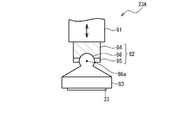
- FIG. 11 is a side view schematically showing the structure of the upper stage mechanism 23A having such a configuration.
- the upper stage mechanism 23 ⁇ / b> A has a lifting rod 81 that is lifted up and down, and holds the upper wafer 33 at the lower end of the lifting rod 81 via an angle adjustment mechanism 82.
- An electrostatic chuck 83 is attached.
- the angle adjustment mechanism 82 includes a ball seat 84 connected to the lower end of the lifting rod 81, a fixing flange 85, and a ball flange 86 attached to the electrostatic chuck 83.
- the spherical flange 86 has a support portion and a flange portion, and the support portion is joined to the electrostatic chuck 83.
- the flange portion is formed in a sphere centered on the point 86a.
- the ball seat 84 has a ball seat surface that is in close contact with the flange portion of the ball flange 86.
- the fixing flange 85 is joined to the ball seat 84 by a fastener exemplified by a bolt, and sandwiches the flange portion of the ball flange 86 so that the flange portion is brought into close contact with the ball seat surface of the ball seat 84.
- the flange portion of the ball flange 86 is slidably connected to the ball seat surface of the ball seat 84 by the fixing flange 85.
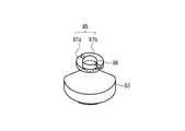
- FIG. 12 is a perspective view showing the structure of the fixing flange 85.
- the fixing flange 85 includes split rings 87a and 87b.
- Each of the split rings 87a and 87b has a shape that forms a part of the ring.
- Each of the split rings 87a and 87b is connected to the ball seat 84 by a fastener exemplified by a bolt.
- the split rings 87a and 87b are arranged so that the inner sides thereof are in contact with the flange portions of the spherical flange 86, and sandwich the flange portions.
- the upper wafer 33 and the lower wafer 34 are maintained while maintaining the parallelism between the upper wafer 33 and the lower wafer 34.
- the side wafer 34 can be bonded. This is effective for uniformly applying a large bonding load between the upper wafer 33 and the lower wafer 34.
Abstract
The normal temperature bonding device is equipped with a bonding chamber, an upper side stage mechanism whereby an upper side wafer is supported in such a way as to be vertically movable inside the bonding chamber, and a lower side stage mechanism whereby a lower side wafer is supported in such a way as to be movable within a horizontal plane inside the bonding chamber. The lower side stage mechanism comprises a carriage having a lower side wafer holding part for holding the lower side wafer, an elastic guide coupled to the carriage and supporting the carriage, a positioning stage for coarsely moving the lower side wafer holding part, a fine movement mechanism for finely moving the lower side wafer holding part, and a carriage support block. The elastic guide supports the carriage in such a manner that the carriage does not come into contact with the carriage support block when no load is being applied from the upper side stage mechanism onto the carriage, and elastically deforms so that the carriage comes into contact with the carriage support block when the upper side stage mechanism brings the upper side wafer into contact with the lower side wafer, thereby applying a vertical load onto the carriage.
Description
本発明は、常温接合装置に関する。
The present invention relates to a room temperature bonding apparatus.
2枚のウェハ(基板)を接合するための技術として、常温接合が知られている。常温接合とは、接合すべき2枚のウェハの表面を真空雰囲気で活性化し、活性化されたウェハ表面を接触させることで該2枚のウェハを接合する技術である。ウェハ表面を活性化する手法としては、例えば、イオンビームを用いる方法と中性原子ビームを用いる方法とが知られている。
Room temperature bonding is known as a technique for bonding two wafers (substrates). The room temperature bonding is a technique in which the surfaces of two wafers to be bonded are activated in a vacuum atmosphere, and the two wafers are bonded by bringing the activated wafer surfaces into contact with each other. As a method for activating the wafer surface, for example, a method using an ion beam and a method using a neutral atom beam are known.
常温接合における基礎技術の一つが、接合されるウェハの位置合わせである。近年では、デバイスの小型化、高精度化が進んでおり、接合されるウェハを精密に位置合わせすることが重要になってきている。ウェハの精密な位置合わせを実現する方法としては、圧電素子を用いて位置合わせを行う技術が知られている(例えば、特許第4822577号(特許文献1)、特許第4669766号(特許文献2)参照)。
One of the basic technologies in room temperature bonding is the alignment of wafers to be bonded. In recent years, miniaturization and high precision of devices have progressed, and it has become important to precisely align wafers to be bonded. As a method for realizing precise alignment of a wafer, techniques for performing alignment using a piezoelectric element are known (for example, Japanese Patent No. 4822577 (Patent Document 1) and Japanese Patent No. 4669766 (Patent Document 2)). reference).
圧電素子の使用は、精密な位置合わせに好適であるが、その一方で、十分に大きなストローク(可動範囲)を提供できないという問題がある。このような問題に対処する技術としては、粗動ステージと微動ステージの組み合わせを用いる技術が知られている(例えば、特開2005-288637号公報(特許文献3)、特開平5-160340号公報(特許文献4)参照)。
The use of piezoelectric elements is suitable for precise positioning, but there is a problem that a sufficiently large stroke (movable range) cannot be provided. As a technique for coping with such a problem, a technique using a combination of a coarse movement stage and a fine movement stage is known (for example, Japanese Patent Application Laid-Open No. 2005-288637 (Patent Document 3) and Japanese Patent Application Laid-Open No. 5-160340). (See Patent Document 4).
常温接合のウェハの位置合わせに関し、もう一つの重要な事項は、位置合わせに用いられるステージ機構の耐荷重である。常温接合においては、接合されるウェハに大きな接合圧力(例えば、最大、10トンの圧力)を作用させる必要があるので、ウェハの位置合わせに用いられるステージ機構を、大荷重に耐えられるように設計する必要がある。特許3970304号(特許文献5)は、ステージ機構の耐荷重を高めるための技術を開示している。この特許文献に開示されたステージ機構では、ウェハを保持するキャリッジが弾性案内によって位置決めステージに連結されている。更に、位置決めステージとは別にキャリッジ支持台が設けられている。キャリッジに荷重が印加されない状態では、キャリッジがキャリッジ支持台と接触しないように支持される。キャリッジに荷重が印加されると、弾性案内が弾性変形してキャリッジがキャリッジ支持台に接触され、キャリッジ支持台に荷重が分散される。これにより、位置決めステージに作用する荷重が低減されている。
に 関 し Another important issue regarding the alignment of wafers bonded at room temperature is the load resistance of the stage mechanism used for alignment. In room temperature bonding, it is necessary to apply a large bonding pressure (for example, a maximum pressure of 10 tons) to the wafer to be bonded, so the stage mechanism used for wafer alignment is designed to withstand heavy loads. There is a need to. Japanese Patent No. 3970304 (Patent Document 5) discloses a technique for increasing the load resistance of the stage mechanism. In the stage mechanism disclosed in this patent document, a carriage for holding a wafer is connected to a positioning stage by elastic guidance. In addition to the positioning stage, a carriage support is provided. When no load is applied to the carriage, the carriage is supported so as not to contact the carriage support. When a load is applied to the carriage, the elastic guide is elastically deformed, the carriage comes into contact with the carriage support base, and the load is distributed to the carriage support base. Thereby, the load which acts on the positioning stage is reduced.
しかしながら、上述された公知技術は、いずれも、十分に大きなストロークを有しながら、ウェハの精密な位置合わせとステージ機構の耐荷重の増大の要求をも満たすステージ機構を提供するものではない。
However, none of the above-described known techniques provide a stage mechanism that satisfies the requirements for precise wafer alignment and increased load resistance of the stage mechanism while having a sufficiently large stroke.
なお、本願に関連し得る技術として、試料台の向きを調節する角度調節機構が上側ステージに設けられた常温接合装置が、特許第4209457号(特許文献6)に開示されている。
As a technique that can be related to the present application, Japanese Patent No. 4209457 (Patent Document 6) discloses a room temperature bonding apparatus in which an angle adjustment mechanism for adjusting the orientation of a sample stage is provided on the upper stage.
したがって、本発明の目的は、大きなストロークを有しながら、ウェハの精密な位置合わせと大きな耐荷重の要求をも満たすステージ機構を備えた常温接合装置を提供することにある。
Therefore, an object of the present invention is to provide a room temperature bonding apparatus having a stage mechanism that satisfies the requirements of precise alignment of wafers and large load resistance while having a large stroke.
本発明の一の観点では、常温接合装置が、接合チャンバと、接合チャンバの内部で上側ウェハを上下方向に移動可能に支持する上側ステージ機構と、接合チャンバの内部で下側ウェハを水平面内で移動可能に支持する下側ステージ機構とを具備する。下側ステージ機構は、下側ウェハを保持する下側ウェハ保持部を有するキャリッジと、キャリッジに連結されてキャリッジを支持する弾性案内と、下側ウェハ保持部を粗動させる位置決めステージと、下側ウェハ保持部を微動させる微動機構と、キャリッジ支持台とを含む。弾性案内は、上側ステージ機構からキャリッジに荷重が印加されていないときにキャリッジがキャリッジ支持台に接触しないようにキャリッジを支持し、上側ステージ機構によって上側ウェハが下側ウェハに接触されてキャリッジに上下方向に荷重が印加されるとキャリッジがキャリッジ支持台に接触するように弾性変形する。
In one aspect of the present invention, a room temperature bonding apparatus includes a bonding chamber, an upper stage mechanism that supports the upper wafer so as to be movable in the vertical direction inside the bonding chamber, and the lower wafer within the horizontal plane within the bonding chamber. And a lower stage mechanism that is movably supported. The lower stage mechanism includes a carriage having a lower wafer holding unit for holding the lower wafer, an elastic guide connected to the carriage to support the carriage, a positioning stage for coarsely moving the lower wafer holding unit, and a lower side A fine movement mechanism for finely moving the wafer holding unit and a carriage support base are included. The elastic guide supports the carriage so that the carriage does not contact the carriage support when no load is applied to the carriage from the upper stage mechanism, and the upper stage mechanism makes the upper wafer contact the lower wafer and move up and down the carriage. When a load is applied in the direction, the carriage is elastically deformed so as to contact the carriage support.
一実施形態では、位置決めステージは、弾性案内を駆動することによって下側ウェハ保持部を粗動させ、微動機構が、キャリッジに組み込まれる。
In one embodiment, the positioning stage coarsely moves the lower wafer holder by driving the elastic guide, and the fine movement mechanism is incorporated in the carriage.
一実施形態では、キャリッジが、弾性案内が接合されたキャリッジプレートを含んでおり、下側ウェハ保持部がキャリッジプレートの上方に位置し、微動機構が、キャリッジプレートの上に設けられたフレームと、フレームに連結され下側ウェハ保持部を駆動する駆動機構とを含んでいてもよい。この場合、上側ステージ機構によって上側ウェハが下側ウェハに接触されてキャリッジに前記上下方向に荷重が印加されると、弾性案内は、キャリッジプレートがキャリッジ支持台に接触するように弾性変形する。
In one embodiment, the carriage includes a carriage plate to which elastic guides are joined, the lower wafer holding portion is located above the carriage plate, and the fine movement mechanism is a frame provided on the carriage plate; And a drive mechanism connected to the frame for driving the lower wafer holder. In this case, when the upper wafer is brought into contact with the lower wafer by the upper stage mechanism and a load is applied to the carriage in the vertical direction, the elastic guide is elastically deformed so that the carriage plate comes into contact with the carriage support.
このとき、フレームには、下側ウェハ保持部を上下方向に移動可能に支持する支持機構が設けられてもよい。一実施形態では、支持機構は、上側ステージ機構から下側ウェハ保持部に荷重が印加されていないときに下側ウェハ保持部がキャリッジプレートに接触しないように下側ウェハ保持部を支持し、上側ステージ機構によって上側ウェハが下側ウェハに接触されて下側ウェハ保持部に上下方向に荷重が印加されると下側ウェハ保持部がキャリッジプレートに接触するように弾性変形してもよい。
At this time, the frame may be provided with a support mechanism for supporting the lower wafer holding portion so as to be movable in the vertical direction. In one embodiment, the support mechanism supports the lower wafer holder so that the lower wafer holder does not contact the carriage plate when no load is applied from the upper stage mechanism to the lower wafer holder. When the upper wafer is brought into contact with the lower wafer by the stage mechanism and a load is applied in the vertical direction to the lower wafer holder, the lower wafer holder may be elastically deformed so as to come into contact with the carriage plate.
他の実施形態では、微動機構が、テーブルと、テーブルを駆動する駆動機構とを含み、弾性案内が、下側ウェハ保持部をテーブルに連結してもよい。この場合、位置決めステージは、微動機構の全体を駆動することによって下側ウェハ保持部を粗動させ、微動機構は、駆動機構によってテーブルを駆動することによって下側ウェハ保持部を微動させることが好ましい。
In another embodiment, the fine movement mechanism may include a table and a drive mechanism that drives the table, and the elastic guide may connect the lower wafer holding unit to the table. In this case, it is preferable that the positioning stage coarsely moves the lower wafer holding unit by driving the entire fine movement mechanism, and the fine movement mechanism finely moves the lower wafer holding unit by driving the table by the driving mechanism. .
上記の常温接合装置において、上側ステージ機構は、上側ウェハを保持する上側ウェハ保持部と、上側ウェハ保持部の向きを調節する角度調節機構とを具備していても良い。一実施形態では、上側ステージ機構が、上下方向に昇降される昇降ロッドを備える。この場合、角度調節機構は、上側ウェハ保持部に固定される球フランジと、昇降ロッドに固定される球座と、球座に固定され、球フランジを挟持して球フランジを球座に連結する固定フランジとを含むことが好ましい。
In the above room temperature bonding apparatus, the upper stage mechanism may include an upper wafer holding part that holds the upper wafer and an angle adjustment mechanism that adjusts the direction of the upper wafer holding part. In one embodiment, the upper stage mechanism includes an elevating rod that moves up and down. In this case, the angle adjusting mechanism includes a ball flange fixed to the upper wafer holding unit, a ball seat fixed to the elevating rod, and a ball seat, and the ball flange is clamped to connect the ball flange to the ball seat. It preferably includes a fixed flange.
上記実施形態によれば、大きなストロークを有しながら、ウェハの精密な位置合わせと大きな耐荷重の要求をも満たすステージ機構を備えた常温接合装置を提供することができる。
According to the above-described embodiment, it is possible to provide a room temperature bonding apparatus provided with a stage mechanism that satisfies the requirements for precise alignment of wafers and large load resistance while having a large stroke.
以下、添付図面を参照しながら本発明の実施形態について説明する。なお、以下の説明において、同一又は対応する構成要素は、同一又は対応する符号で参照されることに留意されたい。
Hereinafter, embodiments of the present invention will be described with reference to the accompanying drawings. It should be noted that in the following description, the same or corresponding components are referred to by the same or corresponding reference numerals.
(第1の実施形態)
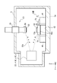
図1は、第1の実施形態の常温接合装置1の構成を示す模式的に示す断面図である。なお、以下の説明においては、必要に応じて、XYZ直交座標系が用いられる。Z軸は、上下方向(鉛直方向)に規定され、X軸は、水平面に平行な面内の特定方向に規定され、Y軸は、X軸、Z軸に垂直な方向に規定される。 (First embodiment)
FIG. 1 is a cross-sectional view schematically showing a configuration of a roomtemperature bonding apparatus 1 according to the first embodiment. In the following description, an XYZ orthogonal coordinate system is used as necessary. The Z axis is defined in the vertical direction (vertical direction), the X axis is defined in a specific direction in a plane parallel to the horizontal plane, and the Y axis is defined in a direction perpendicular to the X axis and the Z axis.
図1は、第1の実施形態の常温接合装置1の構成を示す模式的に示す断面図である。なお、以下の説明においては、必要に応じて、XYZ直交座標系が用いられる。Z軸は、上下方向(鉛直方向)に規定され、X軸は、水平面に平行な面内の特定方向に規定され、Y軸は、X軸、Z軸に垂直な方向に規定される。 (First embodiment)
FIG. 1 is a cross-sectional view schematically showing a configuration of a room
常温接合装置1は、常温接合を実施するプロセスモジュール2と、プロセスモジュール2を制御する制御装置(制御盤)3とを具備している。
The room temperature bonding apparatus 1 includes a process module 2 that performs room temperature bonding and a control device (control panel) 3 that controls the process module 2.
プロセスモジュール2は、ロードロックチャンバ4と接合チャンバ5とを具備している。ロードロックチャンバ4は、外部環境と接合チャンバ5との間のウェハの受け渡しに用いられるチャンバであり、接合チャンバ5は、ウェハの接合が実際に行われるチャンバである。
The process module 2 includes a load lock chamber 4 and a bonding chamber 5. The load lock chamber 4 is a chamber used for transferring a wafer between the external environment and the bonding chamber 5, and the bonding chamber 5 is a chamber in which the wafer is actually bonded.
プロセスモジュール2は、更に、搬送通路6とゲートバルブ7とを備えている。搬送通路6は、ロードロックチャンバ4と接合チャンバ5との間に介設され、接合チャンバ5の内部空間とロードロックチャンバ4の内部空間とを接続している。ゲートバルブ7は、制御装置3による制御の下、搬送通路6を閉鎖し、または、搬送通路6を開放する。即ち、ゲートバルブ7は、ロードロックチャンバ4の内部空間を、接合チャンバ5の内部空間と連通させ、又は、分離する機能を有している。
The process module 2 further includes a transfer passage 6 and a gate valve 7. The conveyance path 6 is interposed between the load lock chamber 4 and the bonding chamber 5, and connects the internal space of the bonding chamber 5 and the internal space of the load lock chamber 4. The gate valve 7 closes the transport passage 6 or opens the transport passage 6 under the control of the control device 3. That is, the gate valve 7 has a function of communicating or separating the internal space of the load lock chamber 4 with the internal space of the bonding chamber 5.
ロードロックチャンバ4は、蓋(図示されない)と真空排気装置11とを備えている。その蓋は、ユーザに操作されることにより、外部環境とロードロックチャンバ4の内部とを接続する開口部(図示されず)を閉鎖し、または、その開口部を開放する。真空排気装置11は、制御装置3による制御の下、ロードロックチャンバ4の内部から気体を排気する。
The load lock chamber 4 includes a lid (not shown) and a vacuum exhaust device 11. The lid is operated by a user to close an opening (not shown) connecting the external environment and the inside of the load lock chamber 4 or open the opening. The vacuum exhaust device 11 exhausts gas from the inside of the load lock chamber 4 under the control of the control device 3.
ロードロックチャンバ4は、さらに、カートリッジ台12、13と搬送ロボット14とを内部に収容している。カートリッジ台12、13には、それぞれ、接合されるウェハを保持するカートリッジ31、32が載せられる。ここで、カートリッジ31は、ウェハの接合の際に、上側に位置するウェハ(以下、上側ウェハ33ということがある)を保持するカートリッジであり、カートリッジ32は、下側に位置するウェハ(以下、下側ウェハ34ということがある)を保持するカートリッジである。搬送ロボット14は、ゲートバルブ7が開放されているときに、搬送通路6を介してカートリッジ台12、13に配置されたカートリッジ31、32を接合チャンバ5の内部に搬送し、または、接合チャンバ5の内部にあるカートリッジ31、32をカートリッジ台12、13に搬送する。
The load lock chamber 4 further accommodates cartridge bases 12 and 13 and a transfer robot 14 inside. Cartridges 31 and 32 holding wafers to be bonded are mounted on the cartridge bases 12 and 13, respectively. Here, the cartridge 31 is a cartridge that holds a wafer positioned on the upper side (hereinafter also referred to as the upper wafer 33) when the wafers are bonded, and the cartridge 32 is a wafer positioned on the lower side (hereinafter referred to as the upper wafer 33). A cartridge for holding the lower wafer 34). When the gate valve 7 is opened, the transfer robot 14 transfers the cartridges 31 and 32 arranged on the cartridge bases 12 and 13 through the transfer path 6 to the inside of the bonding chamber 5 or the bonding chamber 5. Are transported to cartridge bases 12 and 13.
接合チャンバ5は、真空排気装置21を備えている。真空排気装置21は、制御装置3による制御の下、接合チャンバ5の内部から気体を排気する。
The bonding chamber 5 includes a vacuum exhaust device 21. The vacuum exhaust device 21 exhausts gas from the inside of the bonding chamber 5 under the control of the control device 3.
図2は、接合チャンバ5の構造を模式的に示す断面図である。図2に図示されているように、接合チャンバ5は、さらにイオンガン22と、上側ステージ機構23と、下側ステージ機構24とを備えている。イオンガン22は、ウェハの表面の活性化に用いられるイオンビーム22aを出射する。イオンビーム22aが照射されることで、上側ステージ機構23に支持される上側ウェハ33と、下側ステージ機構24に支持される下側ウェハ34の表面の活性化が行われる。なお、本実施形態では、一つのイオンガン22がウェハの表面の活性化に使用されるが、複数のイオンガン22が使用されてもよい。また、イオンガン22の代わりに、他の活性化手段(例えば、中性原子ビーム源)がウェハの活性化に用いられても良い。
FIG. 2 is a cross-sectional view schematically showing the structure of the bonding chamber 5. As shown in FIG. 2, the bonding chamber 5 further includes an ion gun 22, an upper stage mechanism 23, and a lower stage mechanism 24. The ion gun 22 emits an ion beam 22a used for activating the surface of the wafer. Irradiation with the ion beam 22 a activates the surfaces of the upper wafer 33 supported by the upper stage mechanism 23 and the lower wafer 34 supported by the lower stage mechanism 24. In this embodiment, one ion gun 22 is used for activating the surface of the wafer, but a plurality of ion guns 22 may be used. Further, instead of the ion gun 22, other activating means (for example, a neutral atom beam source) may be used for activating the wafer.
上側ステージ機構23は、上側ウェハ33の位置合わせを行うための機構であり、静電チャック25と圧接機構26とを備えている。静電チャック25は、上側ウェハ33を保持する上側ウェハ保持部として機能する。詳細には、静電チャック25は、誘電体層を備えており、その誘電体層の下端に、上下方向(Z軸方向)に概ね垂直な平坦な面を有している。静電チャック25は、さらに、その誘電体層の内部に配置される内部電極を備えている。静電チャック25は、制御装置3による制御の下、その内部電極に所定の印加電圧を印加して、その誘電層の平坦な面の近傍に配置される上側ウェハ33を静電力によって保持する。
The upper stage mechanism 23 is a mechanism for aligning the upper wafer 33, and includes an electrostatic chuck 25 and a pressure contact mechanism 26. The electrostatic chuck 25 functions as an upper wafer holding unit that holds the upper wafer 33. Specifically, the electrostatic chuck 25 includes a dielectric layer, and has a flat surface substantially perpendicular to the vertical direction (Z-axis direction) at the lower end of the dielectric layer. The electrostatic chuck 25 further includes an internal electrode disposed inside the dielectric layer. The electrostatic chuck 25 applies a predetermined applied voltage to the internal electrode under the control of the control device 3 and holds the upper wafer 33 disposed in the vicinity of the flat surface of the dielectric layer by electrostatic force.
圧接機構26は、制御装置3による制御の下、上下方向(Z軸方向)に静電チャック25を昇降させる。一実施形態では、圧接機構26は、制御装置3による制御の下、静電チャック25を所望の位置に位置合わせする。圧接機構26は、さらに、制御装置3による制御の下、静電チャック25の位置(即ち、上側ウェハ33の位置)を測定し、その位置を示すデータを制御装置3に出力する。圧接機構26は、さらに、制御装置3による制御の下、静電チャック25により保持された上側ウェハ33に印加される荷重を測定し、その荷重を示すデータを制御装置3に出力する。
The pressure contact mechanism 26 raises and lowers the electrostatic chuck 25 in the vertical direction (Z-axis direction) under the control of the control device 3. In one embodiment, the pressure contact mechanism 26 aligns the electrostatic chuck 25 at a desired position under the control of the control device 3. The pressure contact mechanism 26 further measures the position of the electrostatic chuck 25 (that is, the position of the upper wafer 33) under the control of the control device 3, and outputs data indicating the position to the control device 3. The pressure contact mechanism 26 further measures a load applied to the upper wafer 33 held by the electrostatic chuck 25 under the control of the control device 3, and outputs data indicating the load to the control device 3.
下側ステージ機構24は、下側ウェハ34の位置合わせを行うための機構であり、その上に載せられたカートリッジ32を保持し、これにより、該カートリッジ32の上に保持された下側ウェハ34を保持する。下側ステージ機構24の詳細については後述する。
The lower stage mechanism 24 is a mechanism for aligning the lower wafer 34, holds the cartridge 32 placed thereon, and thereby the lower wafer 34 held on the cartridge 32. Hold. Details of the lower stage mechanism 24 will be described later.
接合チャンバ5は、更に、アライメント機構27を備えている。アライメント機構27は、上側ステージ機構23によって保持された上側ウェハ33及び下側ステージ機構24に載せられた下側ウェハ34の表面に設けられたアライメントマークの近傍の画像を撮像する。撮像した画像は、制御装置3に送られて画像処理が行われ、これにより、上側ウェハ33と下側ウェハ34の間のXY面内の位置のずれ、及び、XY面内における向きのずれを検出する。アライメント機構27の詳細については後述する。アライメント機構27を用いて得られた上側ウェハ33と下側ウェハ34の間の位置及び向きのずれは、下側ステージ機構24の制御に用いられる。
The bonding chamber 5 further includes an alignment mechanism 27. The alignment mechanism 27 captures an image near the alignment mark provided on the surface of the upper wafer 33 held by the upper stage mechanism 23 and the lower wafer 34 placed on the lower stage mechanism 24. The captured image is sent to the control device 3 to be subjected to image processing, whereby the positional deviation in the XY plane and the positional deviation in the XY plane between the upper wafer 33 and the lower wafer 34 are detected. To detect. Details of the alignment mechanism 27 will be described later. The positional and orientation shift between the upper wafer 33 and the lower wafer 34 obtained by using the alignment mechanism 27 is used for controlling the lower stage mechanism 24.
図3は、本実施形態における制御装置3の構成を模式的に示すブロック図である。制御装置3は、コンピュータに例示される情報処理装置であり、CPU(Central Processing Unit)91と、メモリ92と、入力装置93と、出力装置94と、インターフェース95と、外部記憶装置96と、ドライブ97とを備えている。CPU91、メモリ92、入力装置93、出力装置94、インターフェース95、外部記憶装置96及びドライブ97は、互いに通信可能に接続されている。
FIG. 3 is a block diagram schematically showing the configuration of the control device 3 in the present embodiment. The control device 3 is an information processing device exemplified by a computer, and includes a CPU (Central Processing Unit) 91, a memory 92, an input device 93, an output device 94, an interface 95, an external storage device 96, and a drive. 97. The CPU 91, the memory 92, the input device 93, the output device 94, the interface 95, the external storage device 96, and the drive 97 are connected to be communicable with each other.
CPU91は、外部記憶装置96にインストールされたコンピュータプログラム96aをメモリ92に展開する。CPU91は、更に、展開されたコンピュータプログラム96aを実行して、必要に応じて入力装置93、出力装置94、外部記憶装置96等のハードウェアを制御しながら、コンピュータプログラム96aの情報処理を実現する。
The CPU 91 expands the computer program 96 a installed in the external storage device 96 in the memory 92. The CPU 91 further executes the expanded computer program 96a to realize information processing of the computer program 96a while controlling hardware such as the input device 93, the output device 94, and the external storage device 96 as necessary. .
外部記憶装置96は、コンピュータプログラム96aを記録するとともに、CPU91が利用する情報や生成する情報を記録する。外部記憶装置96へのコンピュータプログラム96aのインストールには、例えば、コンピュータプログラム96aを記録した記録媒体98が用いられてもよい。ドライブ97によってコンピュータプログラム96aが読み込まれ、読み込まれたコンピュータプログラム96aが外部記憶装置96に書き込まれる。
The external storage device 96 records the computer program 96a and also records information used by the CPU 91 and information to be generated. For the installation of the computer program 96a in the external storage device 96, for example, a recording medium 98 on which the computer program 96a is recorded may be used. The computer program 96 a is read by the drive 97, and the read computer program 96 a is written to the external storage device 96.
入力装置93は、ユーザに操作されることにより生成される情報をCPU91や外部記憶装置96に出力する。出力装置94は、CPU91により生成された情報や外部記憶装置96の情報をユーザに認識可能に出力する。
The input device 93 outputs information generated by being operated by the user to the CPU 91 and the external storage device 96. The output device 94 outputs information generated by the CPU 91 and information in the external storage device 96 so that the user can recognize it.
インターフェース95は、プロセスモジュール2の各機器と制御装置3との間の通信に用いられる。具体的には、インターフェース95は、ゲートバルブ7、搬送ロボット14、真空排気装置11、21、イオンガン22、上側ステージ機構23(即ち、静電チャック25及び圧接機構26)及び下側ステージ機構24を制御する制御信号を送信し、また、これらの機器から送信される信号を受け取る。
The interface 95 is used for communication between each device of the process module 2 and the control device 3. Specifically, the interface 95 includes the gate valve 7, the transfer robot 14, the vacuum exhaust devices 11 and 21, the ion gun 22, the upper stage mechanism 23 (that is, the electrostatic chuck 25 and the pressure contact mechanism 26), and the lower stage mechanism 24. Control signals to be controlled are transmitted, and signals transmitted from these devices are received.
制御装置3にインストールされるコンピュータプログラム96aは、制御装置3に所望の機能を実現させるためのプログラムコード群を含んでいる。第1に、該プログラムコード群は、ウェハ33、34の搬送、設置および取り出しに関してプロセスモジュール2を制御する機能を提供する。この機能では、主として、ロードロックチャンバ4の真空排気装置11の制御、ゲートバルブ7の開閉の制御、搬送ロボット14によるカートリッジ31、32の搬送の制御、静電チャック25の制御及び圧接機構26の制御が行われる。第2に、該プログラムコード群は、ウェハ33、34の活性化に関してプロセスモジュール2を制御する機能を提供する。この機能では、主として、接合チャンバ5の真空排気装置21の制御、圧接機構26の制御、イオンガン22の制御が行われる。第3に、該プログラムコード群は、ウェハ33、34の接合に関してプロセスモジュール2を制御する機能を提供する。この機能では、主として、静電チャック25の制御及び圧接機構26の制御及び下側ステージ機構24の制御が行われる。
The computer program 96a installed in the control device 3 includes a program code group for causing the control device 3 to realize a desired function. First, the program code group provides a function of controlling the process module 2 with respect to the transfer, installation and removal of the wafers 33 and 34. In this function, mainly control of the vacuum exhaust device 11 of the load lock chamber 4, control of opening / closing of the gate valve 7, control of transport of the cartridges 31 and 32 by the transport robot 14, control of the electrostatic chuck 25, and press-contact mechanism 26 Control is performed. Second, the program code group provides a function of controlling the process module 2 with respect to the activation of the wafers 33 and 34. In this function, control of the vacuum exhaust device 21 of the bonding chamber 5, control of the pressure contact mechanism 26, and control of the ion gun 22 are mainly performed. Third, the program code group provides a function of controlling the process module 2 with respect to the bonding of the wafers 33 and 34. In this function, control of the electrostatic chuck 25, control of the pressure contact mechanism 26, and control of the lower stage mechanism 24 are mainly performed.
本実施形態の常温接合装置1の一つの特徴は、下側ステージ機構24の構成にある。本実施形態では、下側ステージ機構24が、十分に大きなストロークを提供可能でありながら、ウェハの精密な位置合わせと大きな耐荷重の両方の要求を満たすように構成されている。以下、本実施形態における下側ステージ機構24の構成について詳細に説明する。
One feature of the room temperature bonding apparatus 1 of the present embodiment is the configuration of the lower stage mechanism 24. In the present embodiment, the lower stage mechanism 24 is configured to satisfy both requirements of precise alignment of the wafer and a large load resistance while being able to provide a sufficiently large stroke. Hereinafter, the configuration of the lower stage mechanism 24 in the present embodiment will be described in detail.
図4Aは、下側ステージ機構24の構成を概略的に示す模式図である。下側ステージ機構24は、位置決めステージ41と、キャリッジ支持台42と、キャリッジ43と、弾性案内44とを備えている。位置決めステージ41及びキャリッジ支持台42は、接合チャンバ5の底板5aに支持されている。後述されるように、位置決めステージ41は、大きなストロークで下側ウェハ34を粗動させる粗動ステージとして機能する。キャリッジ支持台42は、その上端に平滑な支持面42aを有している。支持面42aは、上下方向(Z軸方向)に垂直である。
FIG. 4A is a schematic diagram schematically showing the configuration of the lower stage mechanism 24. The lower stage mechanism 24 includes a positioning stage 41, a carriage support base 42, a carriage 43, and an elastic guide 44. The positioning stage 41 and the carriage support 42 are supported by the bottom plate 5 a of the bonding chamber 5. As will be described later, the positioning stage 41 functions as a coarse movement stage that coarsely moves the lower wafer 34 with a large stroke. The carriage support base 42 has a smooth support surface 42a at its upper end. The support surface 42a is perpendicular to the vertical direction (Z-axis direction).
キャリッジ43は、その上に載せられたカートリッジ32(及びカートリッジ32に載せられた下側ウェハ34)を保持する。後に詳細に説明するように、本実施形態では、キャリッジ43に、下側ウェハ34を小さなストロークで微動させる微動ステージの機能が組み込まれる。弾性案内44は、弾性体から形成され、キャリッジ43の側面に接合されている。キャリッジ43は、弾性案内44によって位置決めステージ41に連結されている。弾性案内44は、キャリッジ43に荷重が印加されていない状態では、キャリッジ43の下面43aが、キャリッジ支持台42の支持面42aと接触しないようにキャリッジ43を支持する。このとき、キャリッジ43の下面43aとキャリッジ支持台42の支持面42aの間には、100μm程度の隙間が設けられる。一方、上側ステージ機構23によって荷重がキャリッジ43に鉛直下方向に印加されると、弾性案内44は、キャリッジ43の下面43aがキャリッジ支持台42の支持面42aに接触するように弾性変形する。
The carriage 43 holds the cartridge 32 (and the lower wafer 34 placed on the cartridge 32) placed thereon. As will be described in detail later, in the present embodiment, a function of a fine movement stage for finely moving the lower wafer 34 with a small stroke is incorporated in the carriage 43. The elastic guide 44 is formed of an elastic body and is joined to the side surface of the carriage 43. The carriage 43 is connected to the positioning stage 41 by an elastic guide 44. The elastic guide 44 supports the carriage 43 so that the lower surface 43 a of the carriage 43 does not come into contact with the support surface 42 a of the carriage support base 42 when no load is applied to the carriage 43. At this time, a gap of about 100 μm is provided between the lower surface 43 a of the carriage 43 and the support surface 42 a of the carriage support 42. On the other hand, when a load is applied vertically downward to the carriage 43 by the upper stage mechanism 23, the elastic guide 44 is elastically deformed so that the lower surface 43a of the carriage 43 contacts the support surface 42a of the carriage support base 42.
ここで、位置決めステージ41は、弾性案内44、及び、弾性案内44に連結されたキャリッジ43を駆動する、より具体的には、X軸方向、Y軸方向に移動し、且つ、θ角方向に回転するように構成されている。ここで、位置決めステージ41には、例えばボールねじ、リニアガイド、及びモータを用いた移動/回転機構(図示されない)が組み込まれており、位置決めステージ41は、粗動ステージとして機能する。必要がある場合、位置決めステージ41によってキャリッジ43が移動及び/又は回転され、これにより、キャリッジ43の上に載せられたカートリッジ32(及びカートリッジ32に載せられた下側ウェハ34)が移動及び/又は回転される。
Here, the positioning stage 41 drives the elastic guide 44 and the carriage 43 connected to the elastic guide 44. More specifically, the positioning stage 41 moves in the X-axis direction and the Y-axis direction, and in the θ-angle direction. It is configured to rotate. Here, the positioning stage 41 incorporates a moving / rotating mechanism (not shown) using, for example, a ball screw, a linear guide, and a motor, and the positioning stage 41 functions as a coarse movement stage. If necessary, the carriage 43 is moved and / or rotated by the positioning stage 41, so that the cartridge 32 placed on the carriage 43 (and the lower wafer 34 placed on the cartridge 32) is moved and / or moved. It is rotated.
下側ステージ機構24には、上述のアライメント機構27が組み込まれる。図4Bは、下側ステージ機構24のアライメント機構27に関連する部分の構造を示す模式図である。アライメント機構27は、赤外線を発生する赤外照明101と、該赤外線の向きを鉛直方向に変えるレンズ102と、カメラ103とを備えている。更に、キャリッジ支持台42に透明部位104が形成され、キャリッジ43に(より精密には、後述されるように、キャリッジ43のステージ52に)透明部位105が形成されている。透明部位104、105は、いずれも、赤外照明101が照射する赤外線に対して透明な材料で形成されている。キャリッジ43の透明部位105は、キャリッジ支持台42の透明部位104の近傍に配置されている。
The above-described alignment mechanism 27 is incorporated in the lower stage mechanism 24. FIG. 4B is a schematic diagram illustrating a structure of a portion related to the alignment mechanism 27 of the lower stage mechanism 24. The alignment mechanism 27 includes an infrared illumination 101 that generates infrared rays, a lens 102 that changes the direction of the infrared rays to a vertical direction, and a camera 103. Further, a transparent portion 104 is formed on the carriage support 42, and a transparent portion 105 is formed on the carriage 43 (more precisely, on the stage 52 of the carriage 43 as will be described later). The transparent portions 104 and 105 are both made of a material that is transparent to the infrared rays that the infrared illumination 101 irradiates. The transparent portion 105 of the carriage 43 is disposed in the vicinity of the transparent portion 104 of the carriage support base 42.
アライメント機構27は、キャリッジ43の上に乗せられるカートリッジ32に設けられた透明部位106、上側ウェハ33に設けられたアライメントマーク107、及び、下側ウェハ34に設けられたアライメントマーク108を用いて、上側ウェハ33と下側ウェハ34の位置及び向けのずれを検出する。ここで、透明部位106は、赤外照明101が照射する赤外線に対して透明な材料で形成されている。詳細には、レンズ102は、赤外照明101により生成される赤外線の向きを鉛直方向に代えて、赤外線を透明部位104、105、106を介して上側ウェハ33、下側ウェハ34に入射する。一般的にウェハに用いられる絶縁材料(例えば、ガラス)及び半導体(例えば、シリコン)は、赤外線を少なくとも一定程度は通過させる材料であることに留意されたい。レンズ102は、更に、該赤外線が上側ウェハ33及び下側ウェハ34によって反射されて生成された反射光を、カメラ103に入射する。カメラ103は、レンズ102を通過した反射光を撮像し、上側ウェハ33及び下側ウェハ34の一部分の画像(即ち、アライメントマーク107、108の近傍の画像)を得る。得られた画像は制御装置3に送られ、該画像に対して制御装置3によって画像処理が行われる。この画像処理により、上側ウェハ33と下側ウェハ34の位置及び向けのずれが検出される。
The alignment mechanism 27 uses a transparent portion 106 provided on the cartridge 32 placed on the carriage 43, an alignment mark 107 provided on the upper wafer 33, and an alignment mark 108 provided on the lower wafer 34. The position and orientation deviation between the upper wafer 33 and the lower wafer 34 is detected. Here, the transparent portion 106 is formed of a material that is transparent to the infrared rays irradiated by the infrared illumination 101. Specifically, the lens 102 changes the direction of the infrared rays generated by the infrared illumination 101 to the vertical direction, and makes the infrared rays enter the upper wafer 33 and the lower wafer 34 through the transparent portions 104, 105, and 106. Note that insulating materials (eg, glass) and semiconductors (eg, silicon) typically used for wafers are materials that allow infrared light to pass through at least to some extent. The lens 102 further enters the camera 103 with reflected light generated by reflecting the infrared rays by the upper wafer 33 and the lower wafer 34. The camera 103 captures the reflected light that has passed through the lens 102 and obtains images of parts of the upper wafer 33 and the lower wafer 34 (that is, images near the alignment marks 107 and 108). The obtained image is sent to the control device 3, and the control device 3 performs image processing on the image. By this image processing, the position and the deviation of the upper wafer 33 and the lower wafer 34 are detected.
なお、キャリッジ支持台42に透明部位104を設ける代わりに、赤外線を通過させるための空洞(又は穴)を設けてもよい。同様に、キャリッジ43及びカートリッジ32に透明部位105、106を設ける代わりに、赤外線を通過させるための空洞(又は穴)を設けてもよい。一実施形態では、キャリッジ支持台42に透明部位104が設けられ、キャリッジ43及びカートリッジ32に、赤外線を通過させるための空洞が設けられてもよい。
In addition, instead of providing the transparent portion 104 on the carriage support base 42, a cavity (or hole) for allowing infrared light to pass through may be provided. Similarly, instead of providing the transparent portions 105 and 106 in the carriage 43 and the cartridge 32, a cavity (or hole) for allowing infrared rays to pass therethrough may be provided. In one embodiment, the carriage support base 42 may be provided with the transparent portion 104, and the carriage 43 and the cartridge 32 may be provided with a cavity for allowing infrared light to pass through.
続いて、キャリッジ43の構造について詳細に説明する。図5Aは、キャリッジ43の構成を示す平面図である。キャリッジ43は、フレーム51と、テーブル52とを備えている。フレーム51は、上述の弾性案内44によって位置決めステージ41に連結される。
Subsequently, the structure of the carriage 43 will be described in detail. FIG. 5A is a plan view showing the configuration of the carriage 43. The carriage 43 includes a frame 51 and a table 52. The frame 51 is connected to the positioning stage 41 by the elastic guide 44 described above.
テーブル52は、その上に載せられたカートリッジ32(及びカートリッジ32に載せられた下側ウェハ34)を保持する下側ウェハ保持部として用いられる。テーブル52には、上述の透明部位105が形成されている。上述のように、キャリッジ43のテーブル52には透明部位105の代わりに赤外線を通過させるための空洞(又は穴)を設けてもよい。テーブル52は、フレーム51に囲まれて配置されており、複数のヒンジ部53により、フレーム51に可動に支持されている。本実施形態では、テーブル52の4隅が4つのヒンジ部53によってフレーム51に連結されている。
The table 52 is used as a lower wafer holding unit for holding the cartridge 32 (and the lower wafer 34 placed on the cartridge 32) placed thereon. The table 52 is formed with the transparent portion 105 described above. As described above, the table 52 of the carriage 43 may be provided with a cavity (or hole) for allowing infrared light to pass instead of the transparent portion 105. The table 52 is disposed so as to be surrounded by the frame 51, and is movably supported by the frame 51 by a plurality of hinge portions 53. In the present embodiment, four corners of the table 52 are connected to the frame 51 by four hinge portions 53.
図5Bは、ヒンジ部53の構成を示す平面図である。各ヒンジ部53は、小片部材61、62を有している。小片部材61は、狭隘部63によってテーブル52に連結されており、狭隘部64によって小片部材62に連結されている。また、小片部材62は、狭隘部65によってフレーム51に連結されている。図5Cは、狭隘部63の構造を示す斜視図である。狭隘部63は、幅が細い構造として構成されており、湾曲可能である。狭隘部64、65も同様に、幅が細い構造として構成されており、湾曲可能である。このような構造のヒンジ部53は、テーブル52を、X軸方向、Y軸方向に移動可能であり、且つ、θ角方向に回転可能であるようにフレーム51に連結している。ここで、θ角方向とは、XY平面内の角度方向である。
FIG. 5B is a plan view showing the configuration of the hinge portion 53. Each hinge portion 53 has small piece members 61 and 62. The small piece member 61 is connected to the table 52 by the narrowed portion 63 and is connected to the small piece member 62 by the narrowed portion 64. The small piece member 62 is connected to the frame 51 by a narrow portion 65. FIG. 5C is a perspective view showing the structure of the narrow portion 63. The narrow part 63 is configured as a narrow structure and can be bent. Similarly, the narrow portions 64 and 65 are configured as a narrow structure and can be bent. The hinge 53 having such a structure connects the table 52 to the frame 51 so that the table 52 can be moved in the X-axis direction and the Y-axis direction and can be rotated in the θ-angle direction. Here, the θ angle direction is an angle direction in the XY plane.
図5Aに戻り、キャリッジ43は、更に、テーブル52を駆動する3つの駆動機構541~543を備えている。駆動機構541、542は、テーブル52をX軸方向に駆動し、駆動機構543は、テーブル52をY軸方向に駆動する。3つの駆動機構541~543は、テーブル52を微動させる微動機構として用いられる。
Returning to FIG. 5A, the carriage 43 further includes three drive mechanisms 54 1 to 54 3 for driving the table 52. Drive mechanism 54 1, 54 2 drives the table 52 in the X-axis direction, the driving mechanism 543 drives the table 52 in the Y-axis direction. The three drive mechanisms 54 1 to 54 3 are used as fine movement mechanisms for finely moving the table 52.
詳細には、駆動機構541は、圧電素子551と連結部561とを備えている。圧電素子551は、その一端がフレーム51に連結されており、他端が連結部561に連結されている。圧電素子551は、それに供給された電圧に応じて連結部561をX軸方向に移動させる。連結部561は、その一端が圧電素子551に連結され、他端がテーブル52に連結されている。ここで、連結部561は、2つの狭隘部57が設けられ、狭隘部57において湾曲可能である。このような構造により、駆動機構543によってテーブル52がY軸方向に駆動された場合でも、テーブル52のY軸方向への変位を狭隘部57の湾曲によって吸収することができる。
Specifically, the drive mechanism 54 1 includes a piezoelectric element 55 1 and a connecting portion 56 1 . The piezoelectric element 55 1 has one end connected to the frame 51, are connected to the connecting portion 56 1 and the other end. The piezoelectric element 55 1, the connecting portion 56 1 is moved in the X-axis direction in accordance with the supplied voltage to it. Connecting portion 56 1 has its one end connected to the piezoelectric element 55 1, and the other end is connected to the table 52. Here, the connecting portions 56 1, two narrow portion 57 is provided, which is bendable in the narrow portion 57. This structure, by the drive mechanism 54 3 Table 52 even when it is driven in the Y-axis direction can be absorbed by the curvature of the constriction 57 the displacement in the Y-axis direction of the table 52.
駆動機構542も、駆動機構541と同様に構成されており、圧電素子552と連結部562とを備えている。圧電素子552は、その一端がフレーム51に連結されており、他端が連結部562に連結されている。圧電素子552は、それに供給された電圧に応じて連結部562をX軸方向に移動させる。連結部562は、その一端が圧電素子552に連結され、他端がテーブル52に連結されている。連結部562は、2つの狭隘部が設けられており、該狭隘部において湾曲可能である。このような構造により、駆動機構543によってテーブル52がY軸方向に駆動された場合でも、テーブル52のY軸方向への変位を連結部562の狭隘部の湾曲によって吸収することができる。
Drive mechanism 542 also, the driving mechanism 54 1 is configured similarly to, and a piezoelectric element 55 2 and the connecting portion 56 2. The piezoelectric element 55 2 has one end connected to the frame 51, are connected to the connecting portion 56 2 and the other end. The piezoelectric element 55 2, the coupling portion 56 2 is moved in the X-axis direction in accordance with the supplied voltage to it. Connecting portion 56 2 has its one end connected to the piezoelectric element 55 2, and the other end is connected to the table 52. Connecting portion 56 2, the two are narrow portion is provided, it is bendable in said narrow portion. Such a structure table 52 by the drive mechanism 543 even when it is driven in the Y-axis direction can be absorbed by the curvature of the narrow portion of the displacement of the coupling portion 56 2 in the Y-axis direction of the table 52.
更に駆動機構543も、テーブル52を駆動する方向が異なる点を除けば、駆動機構541、542と同様に構成されている。詳細には、駆動機構543は、圧電素子553と連結部563とを備えている。圧電素子553は、その一端がフレーム51に連結されており、他端が連結部563に連結されている。圧電素子553は、それに供給された電圧に応じて連結部563をY軸方向に移動させる。連結部563は、その一端が圧電素子553に連結され、他端がテーブル52に連結されている。連結部563は、2つの狭隘部が設けられており、該狭隘部において湾曲可能である。このような構造により、駆動機構541、542によってテーブル52がX軸方向に駆動された場合でも、テーブル52のX軸方向への変位を連結部563の狭隘部の湾曲によって吸収することができる。
Further the drive mechanism 543 also, except that the direction for driving the table 52 are different, it has the same configuration as the drive mechanism 54 1, 54 2. Specifically, the drive mechanism 543 is provided with a connecting portion 56 3 and the piezoelectric element 55 3. The piezoelectric element 55 3 has one end connected to the frame 51, are connected to the connecting portion 56 3 and the other end. The piezoelectric element 55 3, a connecting portion 56 3 is moved in the Y-axis direction according to the voltage supplied thereto. Connecting portion 56 3 has its one end connected to the piezoelectric element 55 3, and the other end is connected to the table 52. Connecting portion 56 3, two have narrow portion is provided, it is bendable in said narrow portion. This structure, driving mechanism 54 1, by 54 2 even when the table 52 is driven in the X-axis direction, be absorbed by the curvature of the narrow portion of the connecting portion 56 3 a displacement in the X-axis direction of the table 52 Can do.
このような構成のキャリッジ43は、テーブル52を、X軸方向、Y軸方向に移動可能であり、且つ、θ角方向に回転可能である微細ステージとして機能する。X軸方向にテーブル52を移動させる場合、駆動機構541、542の圧電素子551、552に、圧電素子551、552が同一の変位となるような電圧が供給される。これにより、圧電素子551、552に供給される電圧を適切に調節することで、所望の位置にX軸方向にテーブル52を移動させることができる。また、Y軸方向にテーブル52を移動させる場合、駆動機構541、542の圧電素子551、552に、圧電素子551、552が同一の変位となるような電圧が供給される。これにより、圧電素子551、552に供給される電圧を適切に調節することで、所望の位置にX軸方向にテーブル52を移動させることができる。更に、θ角方向にテーブル52を回転させる場合、駆動機構541、542の圧電素子551、552に、圧電素子551、552が異なる変位となるような電圧が供給される。圧電素子551、552に供給される電圧を適切に調節することで、θ角方向の所望の角度にテーブル52を回転させることができる。
The carriage 43 having such a configuration functions as a fine stage that can move the table 52 in the X-axis direction and the Y-axis direction and that can rotate in the θ-angle direction. When moving the X-axis direction on the table 52, the drive mechanism 54 1, 54 2 of the piezoelectric elements 55 1, 55 2, voltages such as a piezoelectric element 55 1, 55 2 have the same displacement is supplied. Accordingly, the table 52 can be moved to the desired position in the X-axis direction by appropriately adjusting the voltage supplied to the piezoelectric elements 55 1 and 55 2 . Also, when moving the Y-axis direction on the table 52, the drive mechanism 54 1, 54 2 of the piezoelectric elements 55 1, 55 2, voltages such as a piezoelectric element 55 1, 55 2 have the same displacement are provided . Accordingly, the table 52 can be moved to the desired position in the X-axis direction by appropriately adjusting the voltage supplied to the piezoelectric elements 55 1 and 55 2 . Furthermore, theta when rotating the table 52 in angular direction, the drive mechanism 54 1, 54 piezoelectric element 55 1 of 2, 55 2, voltages such as a piezoelectric element 55 1, 55 2 is different from the displacement is supplied. By appropriately adjusting the voltage supplied to the piezoelectric elements 55 1 and 55 2 , the table 52 can be rotated to a desired angle in the θ angle direction.
このような構成のキャリッジ43は、テーブル52の移動に圧電素子551、552、553を用いるため、テーブル52を高精度で移動させ、又は、回転させることができる。言い換えれば、キャリッジ43は、テーブル52に載せられたカートリッジ32に保持されている下側ウェハ34の位置合わせを高精度で行うことができる。
Such construction of the carriage 43, for using a piezoelectric element 55 1, 55 2, 55 3 the movement of the table 52, the table 52 is moved at a high precision, or can be rotated. In other words, the carriage 43 can align the lower wafer 34 held by the cartridge 32 placed on the table 52 with high accuracy.
このような構成の下側ステージ機構24による下側ウェハ34の位置決めにおいては、位置決めステージ41が粗動ステージ機構として動作し、キャリッジ43が微動ステージ機構として動作する。即ち、位置決めステージ41は、キャリッジ43と比較して、ストロークが大きいが精度が低いステージ機構として動作する。キャリッジ43は、位置決めステージ41と比較して、ストロークが小さいが精度が高いステージ機構として動作する。下側ウェハ34(及び、下側ウェハ34を保持するカートリッジ32)を大きな変位でX軸方向、Y軸方向、θ角方向の少なくとも一方向に移動させ、又は回転させる必要がある場合、位置決めステージ41によって下側ウェハ34が移動され、又は回転される。また、下側ウェハ34を小さな変位でX軸方向、Y軸方向、θ角方向の少なくとも一方向に移動させ、又は回転させる必要がある場合、キャリッジ43によって下側ウェハ34が移動され、又は回転される。このような動作により、下側ステージ機構24は、十分に大きなストロークと、ウェハの精密な位置合わせとを実現することができる。
In positioning of the lower wafer 34 by the lower stage mechanism 24 having such a configuration, the positioning stage 41 operates as a coarse movement stage mechanism, and the carriage 43 operates as a fine movement stage mechanism. That is, the positioning stage 41 operates as a stage mechanism that has a large stroke but a low accuracy compared to the carriage 43. The carriage 43 operates as a stage mechanism with a smaller stroke but higher accuracy than the positioning stage 41. When the lower wafer 34 (and the cartridge 32 that holds the lower wafer 34) needs to be moved or rotated in at least one of the X axis direction, the Y axis direction, and the θ angle direction with a large displacement, the positioning stage The lower wafer 34 is moved or rotated by 41. When the lower wafer 34 needs to be moved or rotated in at least one of the X axis direction, the Y axis direction, and the θ angle direction with a small displacement, the lower wafer 34 is moved or rotated by the carriage 43. Is done. By such an operation, the lower stage mechanism 24 can realize a sufficiently large stroke and precise alignment of the wafer.
加えて、キャリッジ43が上側ステージ機構23によって鉛直下方向に押された場合、キャリッジ43の下面43aがキャリッジ支持台42の支持面42aに接触し、荷重が主として、キャリッジ支持台42に作用される。したがって、粗動ステージとして機能する位置決めステージ41に作用する荷重が軽減される。このような構造によれば、下側ステージ機構24の耐荷重を増大させることができる。
In addition, when the carriage 43 is pushed vertically downward by the upper stage mechanism 23, the lower surface 43a of the carriage 43 comes into contact with the support surface 42a of the carriage support base 42, and a load is mainly applied to the carriage support base 42. . Therefore, the load acting on the positioning stage 41 that functions as the coarse movement stage is reduced. According to such a structure, the load resistance of the lower stage mechanism 24 can be increased.
続いて、本実施形態における常温接合方法(常温接合装置の動作)について説明する。
図6は、本実施形態における常温接合方法を示すフローチャートである。この常温接合方法は、上述された常温接合装置1を用いて実行される。 Subsequently, a room temperature bonding method (operation of a room temperature bonding apparatus) in the present embodiment will be described.
FIG. 6 is a flowchart showing the room temperature bonding method in the present embodiment. This room temperature bonding method is performed using the roomtemperature bonding apparatus 1 described above.
図6は、本実施形態における常温接合方法を示すフローチャートである。この常温接合方法は、上述された常温接合装置1を用いて実行される。 Subsequently, a room temperature bonding method (operation of a room temperature bonding apparatus) in the present embodiment will be described.
FIG. 6 is a flowchart showing the room temperature bonding method in the present embodiment. This room temperature bonding method is performed using the room
初期状態では、ユーザによって、上側ウェハ33が載せられたカートリッジ31がロードロックチャンバ4のカートリッジ台12に載せられ、下側ウェハ34が載せられたカートリッジ32がカートリッジ台13に載せられているとする。ここで、複数の上側ウェハ33と、それと同数の下側ウェハ34について常温接合が行われる場合には、複数のカートリッジ31がカートリッジ台12に載せられ、同数のカートリッジ32がカートリッジ台13に載せられてもよい。
In an initial state, it is assumed that the cartridge 31 on which the upper wafer 33 is placed is placed on the cartridge base 12 of the load lock chamber 4 and the cartridge 32 on which the lower wafer 34 is placed is placed on the cartridge base 13 by the user. . Here, when room temperature bonding is performed on the plurality of upper wafers 33 and the same number of lower wafers 34, a plurality of cartridges 31 are mounted on the cartridge base 12, and the same number of cartridges 32 are mounted on the cartridge base 13. May be.
まず、ロードロックチャンバ4の蓋が閉鎖され、ロードロックチャンバ4の真空排気装置11により、ロードロックチャンバ4の内部に予備雰囲気が生成される(ステップS1)。予備雰囲気とは、ゲートバルブ7が開放されてロードロックチャンバ4と接合チャンバ5とが搬送通路6を介して連通させることが可能な程度の真空度の雰囲気である。
First, the lid of the load lock chamber 4 is closed, and a preliminary atmosphere is generated inside the load lock chamber 4 by the vacuum exhaust device 11 of the load lock chamber 4 (step S1). The preliminary atmosphere is an atmosphere of a degree of vacuum that allows the load lock chamber 4 and the joining chamber 5 to communicate with each other via the transfer passage 6 by opening the gate valve 7.
続いて、1枚の上側ウェハ33及び1枚の下側ウェハ34が接合チャンバ5に搬送される(ステップS2)。具体的には、まず、ゲートバルブ7が開放され、搬送ロボット14により、上側ウェハ33を載せたカートリッジ31が、ロードロックチャンバ4のカートリッジ台12から接合チャンバ5のキャリッジ43のテーブル52の上に搬送される。続いて、圧接機構26によって静電チャック25が下降される。静電チャック25の下降は、カートリッジ31に載っている上側ウェハ33が静電チャック25に接触するタイミングで停止される。続いて、静電チャック25に上側ウェハ33が保持される。次に、圧接機構26により、静電チャック25が所定の待機位置に位置するまで上昇される。続いて、搬送ロボット14により、カートリッジ31がキャリッジ43からカートリッジ台12に搬送される。その後、搬送ロボット14により、下側ウェハ34が載せられたカートリッジ32がカートリッジ台13からキャリッジ43のテーブル52の上に搬送される。続いて、ゲートバルブ7が閉鎖される。
Subsequently, one upper wafer 33 and one lower wafer 34 are transferred to the bonding chamber 5 (step S2). Specifically, first, the gate valve 7 is opened, and the transfer robot 14 moves the cartridge 31 on which the upper wafer 33 is placed from the cartridge base 12 of the load lock chamber 4 onto the table 52 of the carriage 43 of the bonding chamber 5. Be transported. Subsequently, the electrostatic chuck 25 is lowered by the pressure contact mechanism 26. The lowering of the electrostatic chuck 25 is stopped when the upper wafer 33 placed on the cartridge 31 comes into contact with the electrostatic chuck 25. Subsequently, the upper wafer 33 is held on the electrostatic chuck 25. Next, the electrostatic chuck 25 is raised by the pressure contact mechanism 26 until it is positioned at a predetermined standby position. Subsequently, the cartridge 31 is transported from the carriage 43 to the cartridge base 12 by the transport robot 14. Thereafter, the transfer robot 14 transfers the cartridge 32 on which the lower wafer 34 is placed from the cartridge table 13 onto the table 52 of the carriage 43. Subsequently, the gate valve 7 is closed.
次に、接合チャンバ5の内部に活性化雰囲気が生成される(ステップS3)。より具体的には、真空排気装置21の制御により、接合チャンバ5の内部の真空度が10-5~10-6Pa程度に調節される。
Next, an activation atmosphere is generated inside the bonding chamber 5 (step S3). More specifically, the degree of vacuum inside the bonding chamber 5 is adjusted to about 10 −5 to 10 −6 Pa by the control of the vacuum exhaust device 21.
続いて、上側ウェハ33及び下側ウェハ34の表面が活性化される(ステップS4)。具体的には、イオンガン22からイオンビーム22aが出射され、イオンビーム22aが、上側ウェハ33及び下側ウェハ34の表面に照射される。これにより、上側ウェハ33及び下側ウェハ34の表面がエッチングされる。イオンビーム22aの照射中、接合チャンバ5の内部の真空度は、10-2~10-3Pa程度となる。
Subsequently, the surfaces of the upper wafer 33 and the lower wafer 34 are activated (step S4). Specifically, an ion beam 22 a is emitted from the ion gun 22, and the surfaces of the upper wafer 33 and the lower wafer 34 are irradiated with the ion beam 22 a. Thereby, the surfaces of the upper wafer 33 and the lower wafer 34 are etched. During irradiation with the ion beam 22a, the degree of vacuum inside the bonding chamber 5 is about 10 −2 to 10 −3 Pa.
次に、上側ステージ機構23と下側ステージ機構24とにより、上側ウェハ33と下側ウェハ34との位置合わせが行われる(ステップS5)。具体的には、上側ステージ機構23の圧接機構26によって静電チャック25が下降され、静電チャック25が所定のアライメント位置に配置される。このとき、上側ウェハ33と下側ウェハ34とは、所定の位置合わせ距離だけ離れている。更に、下側ステージ機構24によって下側ウェハ34が移動及び/又は回転され、上側ウェハ33との水平面内での位置合わせが行われる。
Next, alignment of the upper wafer 33 and the lower wafer 34 is performed by the upper stage mechanism 23 and the lower stage mechanism 24 (step S5). Specifically, the electrostatic chuck 25 is lowered by the pressure contact mechanism 26 of the upper stage mechanism 23, and the electrostatic chuck 25 is disposed at a predetermined alignment position. At this time, the upper wafer 33 and the lower wafer 34 are separated by a predetermined alignment distance. Further, the lower wafer mechanism 34 is moved and / or rotated by the lower stage mechanism 24 to perform alignment with the upper wafer 33 in the horizontal plane.
一実施形態では、上側ウェハ33と下側ウェハ34との位置合わせは、下記の手順で行われる。まず、接合チャンバ5に設けられたアライメント機構27を用いて、上側ウェハ33と下側ウェハ34のアライメントマーク107、108の位置のずれ量(X軸方向のずれ量及びY軸方向のずれ量)及び向きのずれ量(θ角方向のずれ量)が算出される。位置のずれ量は、アライメントマーク107、108の位置の差分として算出され、向きのずれ量は、アライメントマーク107、108の角度の差分として算出される。アライメントマークの位置及び向きのずれ量のいずれもが、それぞれに対して決められた基準範囲内である場合には、上側ウェハ33と下側ウェハ34との位置合わせは終了する。
In one embodiment, the alignment of the upper wafer 33 and the lower wafer 34 is performed according to the following procedure. First, using the alignment mechanism 27 provided in the bonding chamber 5, the displacement amount of the alignment marks 107 and 108 on the upper wafer 33 and the lower wafer 34 (deviation amount in the X-axis direction and deviation amount in the Y-axis direction). Then, a deviation amount in the direction (a deviation amount in the θ angle direction) is calculated. The displacement amount of the position is calculated as a difference between the positions of the alignment marks 107 and 108, and the displacement amount of the direction is calculated as a difference between the angles of the alignment marks 107 and 108. When both the position of the alignment mark and the amount of misalignment are within the reference range determined for each, the alignment of the upper wafer 33 and the lower wafer 34 is completed.
一方、アライメントマークの位置のずれ量と向きのずれ量の少なくとも一方が基準範囲外にある場合には、下側ステージ機構24は、このずれ量を解消するように、下側ウェハ34を移動及び/又は回転する。このとき、アライメントマークの位置のずれ量と向きのずれ量の大きさによって、位置決めステージ41による下側ウェハ34の粗動と、キャリッジ43の駆動機構541~543による下側ウェハ34の微動とが、選択的に行われる。詳細には、アライメントマークの位置のずれ量と向きのずれ量の少なくとも一方が、それぞれに対して決められた閾値よりも大きい場合、キャリッジ43が位置決めステージ41によって駆動され、キャリッジ43が移動及び/又は回転される。一方、アライメントマークの位置のずれ量と向きのずれ量の両方が、それぞれに対して決められた閾値よりも小さい場合、テーブル52がキャリッジ43の駆動機構541~543によって駆動される。これにより、テーブル52の上に保持されたカートリッジ32に載せられた下側ウェハ34が、アライメントマークの位置のずれ量と向きのずれ量の解消するように駆動される。キャリッジ43又はテーブル52が移動及び/又は回転された後、アライメントマークの位置及び向きの検出以降の手順が、アライメントマークの位置のずれ量及び向きのずれ量の両方が基準範囲内になるまで繰り返して行われる。
On the other hand, when at least one of the displacement amount of the alignment mark position and the displacement amount of the orientation is outside the reference range, the lower stage mechanism 24 moves and moves the lower wafer 34 so as to eliminate this displacement amount. / Or rotate. At this time, the magnitude of the shift amount and direction of the deviation amount of the position of the alignment mark, and flutter lower wafer 34 by the positioning stage 41, the fine movement of the lower wafer 34 by the driving mechanism 54 1-54 3 the carriage 43 Is selectively performed. Specifically, when at least one of the displacement amount and the displacement amount of the alignment mark is larger than a threshold value determined for each, the carriage 43 is driven by the positioning stage 41, and the carriage 43 is moved and / or moved. Or rotated. On the other hand, both the shift amount and direction of deviation of the position of the alignment mark is less than a threshold value that is determined for each table 52 is driven by a drive mechanism 54 1-54 3 the carriage 43. As a result, the lower wafer 34 placed on the cartridge 32 held on the table 52 is driven so as to eliminate the displacement amount of the alignment mark and the displacement amount thereof. After the carriage 43 or the table 52 is moved and / or rotated, the procedure after the detection of the alignment mark position and orientation is repeated until both the alignment mark position deviation amount and the orientation deviation amount are within the reference range. Done.
続いて、上側ウェハ33と下側ウェハ34とが接触され、上側ウェハ33と下側ウェハ34とが接合される(ステップS6)。具体的には、圧接機構26によって静電チャック25が下降され、上側ウェハ33の表面が下側ウェハ34の表面に接触される。静電チャック25の下降は、静電チャック25に印加される荷重が所定の接合荷重に到達するタイミングで停止される。すなわち、上側ウェハ33と下側ウェハ34とに接合荷重が印加される。上側ウェハ33と下側ウェハ34とは、接合荷重が印加されることによって接合され、1枚の接合ウェハに形成される。接合ウェハへの接合荷重の印加は、所定の接合時間だけ継続して行われる。
Subsequently, the upper wafer 33 and the lower wafer 34 are contacted, and the upper wafer 33 and the lower wafer 34 are bonded (step S6). Specifically, the electrostatic chuck 25 is lowered by the pressure contact mechanism 26, and the surface of the upper wafer 33 is brought into contact with the surface of the lower wafer 34. The lowering of the electrostatic chuck 25 is stopped when the load applied to the electrostatic chuck 25 reaches a predetermined bonding load. That is, a bonding load is applied to the upper wafer 33 and the lower wafer 34. The upper wafer 33 and the lower wafer 34 are bonded to each other by applying a bonding load, and are formed into one bonded wafer. Application of the bonding load to the bonded wafer is continuously performed for a predetermined bonding time.
このとき、キャリッジ43のテーブル52にも鉛直下向き方向に荷重が印加される。テーブル52に荷重が印加されると、弾性案内44が弾性変形し、キャリッジ43の下面43aがキャリッジ支持台42の支持面42aに接触する。この結果、テーブル52に印加された荷重が、主として、キャリッジ支持台42に作用され、位置決めステージ41に作用する荷重が軽減される。これは、下側ステージ機構24の耐荷重を増大させることができることを意味している。
At this time, a load is also applied to the table 52 of the carriage 43 in the vertically downward direction. When a load is applied to the table 52, the elastic guide 44 is elastically deformed, and the lower surface 43 a of the carriage 43 comes into contact with the support surface 42 a of the carriage support base 42. As a result, the load applied to the table 52 is mainly applied to the carriage support 42, and the load applied to the positioning stage 41 is reduced. This means that the load resistance of the lower stage mechanism 24 can be increased.
続いて、接合ウェハがロードロックチャンバ4に搬送される(ステップS7)。具体的には、接合ウェハが静電チャック25から離脱された後、圧接機構26により、静電チャック25が上昇される。このとき、接合ウェハは、カートリッジ32の上に載せられた状態になる。その後、ゲートバルブ7が開放されると、搬送ロボット14により、接合ウェハが載せられたカートリッジ32が、キャリッジ43のテーブル52からロードロックチャンバ4に搬送され、カートリッジ台13に戻される。
Subsequently, the bonded wafer is transferred to the load lock chamber 4 (step S7). Specifically, after the bonded wafer is detached from the electrostatic chuck 25, the electrostatic chuck 25 is raised by the pressure contact mechanism 26. At this time, the bonded wafer is placed on the cartridge 32. Thereafter, when the gate valve 7 is opened, the transfer robot 14 transfers the cartridge 32 on which the bonded wafer is placed from the table 52 of the carriage 43 to the load lock chamber 4 and returns to the cartridge table 13.
まだ接合されていない上側ウェハ33が載せられたカートリッジ31及びまだ接合されていない下側ウェハ34が載せられたカートリッジ32が、カートリッジ台12、13に残存している場合(ステップS8、YES)、ステップS2~ステップS7の動作が、再度、実行される。
When the cartridge 31 on which the upper wafer 33 that has not yet been bonded and the cartridge 32 on which the lower wafer 34 that has not yet been bonded remain on the cartridge bases 12 and 13 (YES in step S8), The operations from step S2 to step S7 are executed again.
一方、全ての上側ウェハ33及び下側ウェハ34の接合が完了している場合(ステップS8、NO)、ロードロックチャンバ4の真空排気装置11が制御され、ロードロックチャンバ4の内部に大気圧雰囲気が生成される(ステップS9)。これにより、ユーザは、ロードロックチャンバ4の蓋を開けて、接合ウェハが載せられたカートリッジ32及び何も載せられていないカートリッジ31を、カートリッジ台12、13から取り出すことができるようになる。以上で、上側ウェハ33と下側ウェハ34の接合の手順が完了する。なお、上述されたステップS1~S9は、制御装置3においてコンピュータプログラム36aが実行されることで実現される。
On the other hand, when the bonding of all the upper wafers 33 and the lower wafers 34 has been completed (step S8, NO), the evacuation device 11 of the load lock chamber 4 is controlled, and the atmospheric pressure atmosphere is set inside the load lock chamber 4. Is generated (step S9). As a result, the user can open the lid of the load lock chamber 4 and take out the cartridge 32 on which the bonded wafer is placed and the cartridge 31 on which nothing is placed from the cartridge bases 12 and 13. Thus, the procedure for bonding the upper wafer 33 and the lower wafer 34 is completed. The above-described steps S1 to S9 are realized by executing the computer program 36a in the control device 3.
以上に説明されているように、本実施形態では、下側ステージ機構24の位置決めステージ41が下側ウェハ34を粗動させる粗動ステージ機構として動作し、キャリッジ43が下側ウェハ34を微動させる微動ステージ機構として動作する。このような動作により、下側ステージ機構24は、十分に大きなストロークと、ウェハの精密な位置合わせとを実現することができる。
As described above, in this embodiment, the positioning stage 41 of the lower stage mechanism 24 operates as a coarse movement stage mechanism that coarsely moves the lower wafer 34, and the carriage 43 finely moves the lower wafer 34. Operates as a fine movement stage mechanism. By such an operation, the lower stage mechanism 24 can realize a sufficiently large stroke and precise alignment of the wafer.
加えて、キャリッジ43が上側ステージ機構23によって鉛直下方向に押された場合、キャリッジ43を支持する弾性案内44が弾性変形し、キャリッジ43の下面43aがキャリッジ支持台42の支持面42aに接触する。この結果、荷重が主として、キャリッジ支持台42に作用される。したがって、粗動ステージ機構として機能する位置決めステージ41に作用する荷重が軽減される。このような構造によれば、下側ステージ機構24の耐荷重を増大させることができる。
In addition, when the carriage 43 is pushed vertically downward by the upper stage mechanism 23, the elastic guide 44 that supports the carriage 43 is elastically deformed, and the lower surface 43a of the carriage 43 contacts the support surface 42a of the carriage support base 42. . As a result, the load is mainly applied to the carriage support base 42. Therefore, the load acting on the positioning stage 41 that functions as the coarse movement stage mechanism is reduced. According to such a structure, the load resistance of the lower stage mechanism 24 can be increased.
(第2の実施形態)
図7は、本発明の第2の実施形態における常温接合装置1の構成、特に、下側ステージ機構24Aの構成を模式的に示す断面図である。第2の実施形態の常温接合装置1の構成は、第1の実施形態の常温接合装置1とほぼ同様である。ただし、下側ステージ機構24Aの構成が、第1の実施形態の下側ステージ機構24の構成と異なっている。なお、第1の実施形態と同様に、下側ステージ24Aにはアライメント機構27が組み込まれてもよいが、図7には図示されていない。 (Second Embodiment)
FIG. 7 is a cross-sectional view schematically showing the configuration of the roomtemperature bonding apparatus 1 according to the second embodiment of the present invention, in particular, the configuration of the lower stage mechanism 24A. The configuration of the room temperature bonding apparatus 1 of the second embodiment is substantially the same as that of the room temperature bonding apparatus 1 of the first embodiment. However, the configuration of the lower stage mechanism 24A is different from the configuration of the lower stage mechanism 24 of the first embodiment. As in the first embodiment, an alignment mechanism 27 may be incorporated in the lower stage 24A, but is not shown in FIG.
図7は、本発明の第2の実施形態における常温接合装置1の構成、特に、下側ステージ機構24Aの構成を模式的に示す断面図である。第2の実施形態の常温接合装置1の構成は、第1の実施形態の常温接合装置1とほぼ同様である。ただし、下側ステージ機構24Aの構成が、第1の実施形態の下側ステージ機構24の構成と異なっている。なお、第1の実施形態と同様に、下側ステージ24Aにはアライメント機構27が組み込まれてもよいが、図7には図示されていない。 (Second Embodiment)
FIG. 7 is a cross-sectional view schematically showing the configuration of the room
詳細には、第2の実施形態では、下側ステージ機構24Aのキャリッジ43Aが、キャリッジプレート46とキャリッジプレート46の上に搭載された微動ステージ47とを備えている。キャリッジプレート46は、弾性案内44によって位置決めステージ41に連結されている。上述のように、位置決めステージ41は、ストロークが大きい粗動ステージとして機能する。キャリッジプレート46は、平滑な上面と平滑な下面とを有している。弾性案内44は、キャリッジ43Aに荷重が印加されていない状態では、キャリッジプレート46の下面が、キャリッジ支持台42の支持面42aと接触しないようにキャリッジプレート46を支持する。このとき、キャリッジプレート46の下面とキャリッジ支持台42の支持面42aの間には、100μm程度の隙間が設けられる。一方、上側ステージ機構23によって荷重がキャリッジ43Aに鉛直下方向に印加されると、弾性案内44は、キャリッジプレート46の下面がキャリッジ支持台42の支持面42aに接触するように弾性変形する。
Specifically, in the second embodiment, the carriage 43A of the lower stage mechanism 24A includes a carriage plate 46 and a fine movement stage 47 mounted on the carriage plate 46. The carriage plate 46 is connected to the positioning stage 41 by an elastic guide 44. As described above, the positioning stage 41 functions as a coarse movement stage having a large stroke. The carriage plate 46 has a smooth upper surface and a smooth lower surface. The elastic guide 44 supports the carriage plate 46 so that the lower surface of the carriage plate 46 does not come into contact with the support surface 42a of the carriage support base 42 when no load is applied to the carriage 43A. At this time, a gap of about 100 μm is provided between the lower surface of the carriage plate 46 and the support surface 42 a of the carriage support base 42. On the other hand, when a load is applied vertically downward to the carriage 43A by the upper stage mechanism 23, the elastic guide 44 is elastically deformed so that the lower surface of the carriage plate 46 contacts the support surface 42a of the carriage support base 42.
微動ステージ47は、図5A~図5Cに図示されているキャリッジ43と同一の構成を有している(ただし、フレーム51は、弾性案内44に直接には連結されていない)。微動ステージ47は、フレーム51と、テーブル52とを備えている。テーブル52は、その上に載せられたカートリッジ32(及びカートリッジ32に載せられた下側ウェハ34)を保持する下側ウェハ保持部として用いられる。テーブル52は、フレーム51に囲まれて配置されており、4つのヒンジ部53により、フレーム51に可動に支持されている。微動ステージ47は、更に、テーブル52を駆動する3つの駆動機構541~543を備えている。駆動機構541、542は、テーブル52をX軸方向に駆動し、駆動機構543は、テーブル52をY軸方向に駆動する。微動ステージ47のフレーム51及びテーブル52の下面は、キャリッジプレート46の上面に接合されている。
The fine movement stage 47 has the same configuration as the carriage 43 shown in FIGS. 5A to 5C (however, the frame 51 is not directly connected to the elastic guide 44). The fine movement stage 47 includes a frame 51 and a table 52. The table 52 is used as a lower wafer holding unit that holds the cartridge 32 (and the lower wafer 34 placed on the cartridge 32) placed thereon. The table 52 is disposed so as to be surrounded by the frame 51, and is movably supported by the frame 51 by four hinge portions 53. Fine movement stage 47 further includes three drive mechanisms 54 1 to 54 3 for driving table 52. Drive mechanism 54 1, 54 2 drives the table 52 in the X-axis direction, the driving mechanism 543 drives the table 52 in the Y-axis direction. The frame 51 of the fine movement stage 47 and the lower surface of the table 52 are joined to the upper surface of the carriage plate 46.
本実施形態の下側ステージ機構24Aの構成でも、第1の実施形態と同様に、十分に大きなストロークを提供可能でありながら、ウェハの精密な位置合わせと大きな耐荷重の要求をも満たすことができる。本実施形態においては、下側ステージ機構24Aの位置決めステージ41が下側ウェハ34を粗動させる粗動ステージ機構として動作する一方で、キャリッジ43Aの微動ステージ47が下側ウェハ34を微動させるために用いられる。このような動作により、下側ステージ機構24は、十分に大きなストロークと、ウェハの精密な位置合わせとを実現することができる。
Even in the configuration of the lower stage mechanism 24A of the present embodiment, it is possible to provide a sufficiently large stroke as well as the first embodiment, while satisfying requirements for precise alignment of the wafer and a large load resistance. it can. In the present embodiment, the positioning stage 41 of the lower stage mechanism 24A operates as a coarse movement stage mechanism that coarsely moves the lower wafer 34, while the fine movement stage 47 of the carriage 43A finely moves the lower wafer 34. Used. By such an operation, the lower stage mechanism 24 can realize a sufficiently large stroke and precise alignment of the wafer.
加えて、キャリッジ43Aが上側ステージ機構23によって鉛直下方向に押された場合、キャリッジプレート46を支持する弾性案内44が弾性変形し、キャリッジプレート46の下面がキャリッジ支持台42の支持面42aに接触する。この結果、荷重が主として、キャリッジ支持台42に作用される。したがって、粗動ステージ機構として機能する位置決めステージ41に作用する荷重が軽減され、下側ステージ機構24の耐荷重を増大させることができる。
In addition, when the carriage 43A is pushed vertically downward by the upper stage mechanism 23, the elastic guide 44 that supports the carriage plate 46 is elastically deformed, and the lower surface of the carriage plate 46 contacts the support surface 42a of the carriage support base 42. To do. As a result, the load is mainly applied to the carriage support base 42. Therefore, the load acting on the positioning stage 41 functioning as the coarse movement stage mechanism is reduced, and the load resistance of the lower stage mechanism 24 can be increased.
図8は、第2の実施形態の常温接合装置1の変形例における下側ステージ機構24Aの構成を模式的に示す断面図である。該変形例においては、微動ステージ47のテーブル52が、ヒンジ部53により、上下方向(Z軸方向)にも移動可能に支持される。ここで、テーブル52は、テーブル52に荷重が印加されていない場合に、テーブル52の下面とキャリッジプレート46の上面との間に隙間があるように支持される。テーブル52の下面とキャリッジプレート46の上面との間に隙間がある構造は、テーブル52の移動の際にテーブル52がキャリッジプレート46と擦れることがないため、微動ステージ47の動作をスムーズにでき、精度低下を防ぐために有効である。また、テーブル52がキャリッジプレート46と擦れることによるパーティクルの発生も抑制できる。
FIG. 8 is a cross-sectional view schematically showing the configuration of the lower stage mechanism 24A in a modification of the room temperature bonding apparatus 1 of the second embodiment. In this modification, the table 52 of the fine movement stage 47 is supported by the hinge portion 53 so as to be movable in the vertical direction (Z-axis direction). Here, the table 52 is supported so that there is a gap between the lower surface of the table 52 and the upper surface of the carriage plate 46 when no load is applied to the table 52. The structure in which there is a gap between the lower surface of the table 52 and the upper surface of the carriage plate 46 prevents the table 52 from rubbing against the carriage plate 46 when the table 52 is moved. This is effective to prevent the accuracy from being reduced. Further, the generation of particles due to the table 52 rubbing against the carriage plate 46 can be suppressed.
ここで、本変形例においては、微動ステージ47のテーブル52が上側ステージ機構23によって鉛直下方向に押されてテーブル52に荷重が印加されると、テーブル52を支持するヒンジ部53が弾性変形し、テーブル52の下面52aがキャリッジプレート46の上面46aに接触する。このとき、キャリッジプレート46も鉛直下方向に押され、キャリッジプレート46の下面が、キャリッジ支持台42の支持面42aに接触する。これにより、荷重が主として、キャリッジ支持台42に作用される。本変形例の構造では、荷重が主としてキャリッジ支持台42に作用することで、微動ステージ47のヒンジ部53に作用する荷重が軽減され、ヒンジ部53の破損を防ぐことができる。
Here, in this modification, when the table 52 of the fine movement stage 47 is pushed vertically downward by the upper stage mechanism 23 and a load is applied to the table 52, the hinge portion 53 that supports the table 52 is elastically deformed. The lower surface 52 a of the table 52 contacts the upper surface 46 a of the carriage plate 46. At this time, the carriage plate 46 is also pushed vertically downward, and the lower surface of the carriage plate 46 comes into contact with the support surface 42 a of the carriage support base 42. Thereby, the load is mainly applied to the carriage support base 42. In the structure of this modified example, the load mainly acts on the carriage support base 42, whereby the load acting on the hinge portion 53 of the fine movement stage 47 is reduced, and the hinge portion 53 can be prevented from being damaged.
(第3の実施形態)
図9は、本発明の第3の実施形態における常温接合装置1の構成、特に、下側ステージ機構24Bの構成を模式的に示す断面図である。第3の実施形態の常温接合装置1の構成は、第1及び第2の実施形態の常温接合装置1と類似している。ただし、下側ステージ機構24Bの構成が、第1の実施形態の下側ステージ機構24及び第2の実施形態の下側ステージ機構24Aの構成と異なっている。なお、第1の実施形態と同様に、下側ステージ24Bにはアライメント機構27が組み込まれてもよいが、図9には図示されていない。 (Third embodiment)
FIG. 9 is a cross-sectional view schematically showing the configuration of the roomtemperature bonding apparatus 1 according to the third embodiment of the present invention, in particular, the configuration of the lower stage mechanism 24B. The configuration of the room temperature bonding apparatus 1 of the third embodiment is similar to that of the room temperature bonding apparatus 1 of the first and second embodiments. However, the configuration of the lower stage mechanism 24B is different from the configurations of the lower stage mechanism 24 of the first embodiment and the lower stage mechanism 24A of the second embodiment. As in the first embodiment, the alignment mechanism 27 may be incorporated in the lower stage 24B, but is not illustrated in FIG.
図9は、本発明の第3の実施形態における常温接合装置1の構成、特に、下側ステージ機構24Bの構成を模式的に示す断面図である。第3の実施形態の常温接合装置1の構成は、第1及び第2の実施形態の常温接合装置1と類似している。ただし、下側ステージ機構24Bの構成が、第1の実施形態の下側ステージ機構24及び第2の実施形態の下側ステージ機構24Aの構成と異なっている。なお、第1の実施形態と同様に、下側ステージ24Bにはアライメント機構27が組み込まれてもよいが、図9には図示されていない。 (Third embodiment)
FIG. 9 is a cross-sectional view schematically showing the configuration of the room
第3の実施形態においては、下側ステージ機構24Bが、位置決めステージ41と、キャリッジ支持台42と、微動ステージ71と、キャリッジ72と、弾性案内73とを備えている。第1及び第2の実施形態と同様に、位置決めステージ41は、ストロークが大きい粗動ステージとして機能する。キャリッジ支持台42は、その上端に平滑な支持面42aを有している。支持面42aは、上下方向(Z軸方向)に垂直である。
In the third embodiment, the lower stage mechanism 24B includes a positioning stage 41, a carriage support base 42, a fine movement stage 71, a carriage 72, and an elastic guide 73. Similar to the first and second embodiments, the positioning stage 41 functions as a coarse movement stage having a large stroke. The carriage support base 42 has a smooth support surface 42a at its upper end. The support surface 42a is perpendicular to the vertical direction (Z-axis direction).
微動ステージ71は、図5A~図5Cに図示されたキャリッジ43(微動ステージ47)と同様の構成を有している。図10に図示されているように、微動ステージ71は、フレーム51と、テーブル52とを備えている。テーブル52は、その上に載せられたカートリッジ32(及びカートリッジ32に載せられた下側ウェハ34)を保持するウェハ保持部として用いられる。テーブル52は、フレーム51に囲まれて配置されており、4つのヒンジ部53により、フレーム51に可動に支持されている。微動ステージ47は、更に、テーブル52を駆動する3つの駆動機構541~543を備えている。駆動機構541、542は、テーブル52をX軸方向に駆動し、駆動機構543は、テーブル52をY軸方向に駆動する。微動ステージ47のフレーム51は、位置決めステージ41の上面に接合されている。
The fine movement stage 71 has the same configuration as the carriage 43 (fine movement stage 47) shown in FIGS. 5A to 5C. As shown in FIG. 10, fine movement stage 71 includes a frame 51 and a table 52. The table 52 is used as a wafer holding unit that holds the cartridge 32 (and the lower wafer 34 placed on the cartridge 32) placed thereon. The table 52 is disposed so as to be surrounded by the frame 51, and is movably supported by the frame 51 by four hinge portions 53. Fine movement stage 47 further includes three drive mechanisms 54 1 to 54 3 for driving table 52. Drive mechanism 54 1, 54 2 drives the table 52 in the X-axis direction, the driving mechanism 543 drives the table 52 in the Y-axis direction. The frame 51 of the fine movement stage 47 is joined to the upper surface of the positioning stage 41.
キャリッジ72は、その上に載せられたカートリッジ32(及びカートリッジ32に載せられた下側ウェハ34)を保持する下側ウェハ保持部として機能する。弾性案内73は、弾性体から形成され、キャリッジ72の側面に接合されている。キャリッジ72は、弾性案内73によって微動ステージ71のテーブル52に連結されている。弾性案内73は、キャリッジ72に荷重が印加されていない状態では、キャリッジ72の下面72aが、キャリッジ支持台42の支持面42aと接触しないようにキャリッジ72を支持する。このとき、キャリッジ72の下面72aとキャリッジ支持台42の支持面42aの間には、100μm程度の隙間が設けられる。一方、上側ステージ機構23によって荷重がキャリッジ72に鉛直下方向に印加されると、弾性案内73は、キャリッジ72の下面72aがキャリッジ支持台42の支持面42aに接触するように弾性変形する。
The carriage 72 functions as a lower wafer holding unit that holds the cartridge 32 (and the lower wafer 34 placed on the cartridge 32) placed thereon. The elastic guide 73 is formed of an elastic body and is joined to the side surface of the carriage 72. The carriage 72 is connected to the table 52 of the fine movement stage 71 by an elastic guide 73. The elastic guide 73 supports the carriage 72 so that the lower surface 72a of the carriage 72 does not come into contact with the support surface 42a of the carriage support base 42 when no load is applied to the carriage 72. At this time, a gap of about 100 μm is provided between the lower surface 72 a of the carriage 72 and the support surface 42 a of the carriage support 42. On the other hand, when a load is applied vertically downward to the carriage 72 by the upper stage mechanism 23, the elastic guide 73 is elastically deformed so that the lower surface 72a of the carriage 72 contacts the support surface 42a of the carriage support base 42.
本実施形態の下側ステージ機構24Bの構成でも、第1の実施形態と同様に、十分に大きなストロークを提供可能でありながら、ウェハの精密な位置合わせと大きな耐荷重の要求をも満たすことができる。本実施形態においては、下側ステージ機構24Bの位置決めステージ41が下側ウェハ34を粗動させる粗動ステージ機構として動作する。即ち、位置決めステージ41は、下側ウェハ34の粗動を行う場合、微動ステージ71の全体を駆動して前記微動ステージを移動し、又は、回転する。微動ステージ71のテーブル52に下側ウェハ34を保持するキャリッジ72が弾性案内73によって連結されているので、微動ステージ71の全体を動かすことにより、下側ウェハ34を動かすことができる。その一方で、微動ステージ71が下側ウェハ34を微動させるために用いられる。下側ウェハ34の微動を行う場合、微動ステージ71の駆動機構541~543が、テーブル52を移動し、又は、回転する。テーブル52に下側ウェハ34を保持するキャリッジ72が弾性案内73によって連結されているので、テーブル52を動かすことにより、下側ウェハ34を動かすことができる。このような動作により、下側ステージ機構24Bは、十分に大きなストロークと、ウェハの精密な位置合わせとを実現することができる。
Even in the configuration of the lower stage mechanism 24B of the present embodiment, it is possible to provide a sufficiently large stroke as well as the first embodiment, while satisfying requirements for precise alignment of the wafer and a large load resistance. it can. In the present embodiment, the positioning stage 41 of the lower stage mechanism 24B operates as a coarse movement stage mechanism that coarsely moves the lower wafer 34. That is, the positioning stage 41 moves or rotates the fine movement stage 71 by driving the entire fine movement stage 71 when the lower wafer 34 is coarsely moved. Since the carriage 72 that holds the lower wafer 34 is connected to the table 52 of the fine movement stage 71 by the elastic guide 73, the lower wafer 34 can be moved by moving the entire fine movement stage 71. On the other hand, the fine movement stage 71 is used to finely move the lower wafer 34. When fine movement of the lower wafer 34 is performed, the driving mechanisms 54 1 to 54 3 of the fine movement stage 71 move or rotate the table 52. Since the carriage 72 that holds the lower wafer 34 on the table 52 is connected by the elastic guide 73, the lower wafer 34 can be moved by moving the table 52. By such an operation, the lower stage mechanism 24B can realize a sufficiently large stroke and precise alignment of the wafer.
加えて、キャリッジ72が上側ステージ機構23によって鉛直下方向に押された場合、キャリッジ72を支持する弾性案内73が弾性変形し、キャリッジ72の下面72aがキャリッジ支持台42の支持面42aに接触する。この結果、荷重が主として、キャリッジ支持台42に作用される。ここで、本実施形態では、粗動ステージ機構として機能する位置決めステージ41に作用する荷重の軽減に加え、微動ステージ71に作用する荷重の軽減の効果も得られることに留意されたい。これは、下側ステージ機構24Bの耐荷重の一層の増大に寄与する。
In addition, when the carriage 72 is pushed vertically downward by the upper stage mechanism 23, the elastic guide 73 that supports the carriage 72 is elastically deformed, and the lower surface 72a of the carriage 72 contacts the support surface 42a of the carriage support base 42. . As a result, the load is mainly applied to the carriage support base 42. Here, it should be noted that in the present embodiment, in addition to reducing the load acting on the positioning stage 41 functioning as the coarse movement stage mechanism, the effect of reducing the load acting on the fine movement stage 71 can also be obtained. This contributes to further increase in the load resistance of the lower stage mechanism 24B.
(上側ステージ機構の変形例)
上記の各実施形態においては、上側ステージ機構23が静電チャック25を上下方向に昇降させる機能しか有していないが、上側ウェハ33を保持する静電チャック(上側ウェハ保持部)の向きを調節する角度調節機構が上側ステージ機構に組み込まれてもよい。図11は、このような構成の上側ステージ機構23Aの構造を模式的に示す側面図である。 (Modification of upper stage mechanism)
In each of the above embodiments, theupper stage mechanism 23 has only a function of moving the electrostatic chuck 25 up and down, but the orientation of the electrostatic chuck (upper wafer holding unit) that holds the upper wafer 33 is adjusted. An angle adjusting mechanism that performs this may be incorporated into the upper stage mechanism. FIG. 11 is a side view schematically showing the structure of the upper stage mechanism 23A having such a configuration.
上記の各実施形態においては、上側ステージ機構23が静電チャック25を上下方向に昇降させる機能しか有していないが、上側ウェハ33を保持する静電チャック(上側ウェハ保持部)の向きを調節する角度調節機構が上側ステージ機構に組み込まれてもよい。図11は、このような構成の上側ステージ機構23Aの構造を模式的に示す側面図である。 (Modification of upper stage mechanism)
In each of the above embodiments, the
図11に示されているように、上側ステージ機構23Aは、上下方向に昇降される昇降ロッド81を有しており、昇降ロッド81の下端に、角度調節機構82を介して上側ウェハ33を保持する静電チャック83が取り付けられている。角度調節機構82は、昇降ロッド81の下端に連結された球座84と、固定フランジ85と、静電チャック83に取り付けられた球フランジ86とを備えている。球フランジ86は、支持部分とフランジ部分とを有しており、該支持部分は、静電チャック83に接合されている。該フランジ部分は、点86aを中心とする球に形成されている。一方、球座84は、球フランジ86のフランジ部分に密着する球座面を有している。固定フランジ85は、ボルトに例示される締結具により球座84に接合されており、球フランジ86のフランジ部分を挟持して、該フランジ部分を球座84の球座面に密着させる。球フランジ86のフランジ部分は、固定フランジ85によって、球座84の球座面に摺動可能に連結されることになる。
As shown in FIG. 11, the upper stage mechanism 23 </ b> A has a lifting rod 81 that is lifted up and down, and holds the upper wafer 33 at the lower end of the lifting rod 81 via an angle adjustment mechanism 82. An electrostatic chuck 83 is attached. The angle adjustment mechanism 82 includes a ball seat 84 connected to the lower end of the lifting rod 81, a fixing flange 85, and a ball flange 86 attached to the electrostatic chuck 83. The spherical flange 86 has a support portion and a flange portion, and the support portion is joined to the electrostatic chuck 83. The flange portion is formed in a sphere centered on the point 86a. On the other hand, the ball seat 84 has a ball seat surface that is in close contact with the flange portion of the ball flange 86. The fixing flange 85 is joined to the ball seat 84 by a fastener exemplified by a bolt, and sandwiches the flange portion of the ball flange 86 so that the flange portion is brought into close contact with the ball seat surface of the ball seat 84. The flange portion of the ball flange 86 is slidably connected to the ball seat surface of the ball seat 84 by the fixing flange 85.
図12は、固定フランジ85の構造を示す斜視図である。固定フランジ85は、分割リング87a、87bを備えている。分割リング87a、87bは、それぞれ、リングの一部を形成するような形状を有している。分割リング87a、87bは、それぞれ、ボルトに例示される締結具により球座84に連結されている。分割リング87a、87bは、その内側が球フランジ86のフランジ部分に接触するように配置され、該フランジ部分を挟持する。
FIG. 12 is a perspective view showing the structure of the fixing flange 85. The fixing flange 85 includes split rings 87a and 87b. Each of the split rings 87a and 87b has a shape that forms a part of the ring. Each of the split rings 87a and 87b is connected to the ball seat 84 by a fastener exemplified by a bolt. The split rings 87a and 87b are arranged so that the inner sides thereof are in contact with the flange portions of the spherical flange 86, and sandwich the flange portions.
このような構造の角度調節機構82を用いて上側ウェハ33を保持する静電チャック83を支持することにより、上側ウェハ33と下側ウェハ34の間の平行度を維持しながら上側ウェハ33と下側ウェハ34とを接合することができる。これは、上側ウェハ33と下側ウェハ34の間に大きな接合荷重を均一に印加するために有効である。
By supporting the electrostatic chuck 83 that holds the upper wafer 33 using the angle adjusting mechanism 82 having such a structure, the upper wafer 33 and the lower wafer 34 are maintained while maintaining the parallelism between the upper wafer 33 and the lower wafer 34. The side wafer 34 can be bonded. This is effective for uniformly applying a large bonding load between the upper wafer 33 and the lower wafer 34.
以上には、本発明の実施形態が具体的に記載されているが、本発明は、上記の実施形態に限定されない。本発明が、様々な変更と共に実施され得ることは、当業者には自明的であろう。
Although the embodiment of the present invention has been specifically described above, the present invention is not limited to the above embodiment. It will be apparent to those skilled in the art that the present invention may be practiced with various modifications.
1 :常温接合装置
2 :プロセスモジュール
3 :制御装置
4 :ロードロックチャンバ
5 :接合チャンバ
5a :底板
6 :搬送通路
7 :ゲートバルブ
11 :真空排気装置
12 :カートリッジ台
13 :カートリッジ台
14 :搬送ロボット
21 :真空排気装置
22 :イオンガン
22a :イオンビーム
23、23A:上側ステージ機構
24、24A、24B:下側ステージ機構
25 :静電チャック
26 :圧接機構
27 :アライメント機構
27a :光学系
27b :撮像装置
27c :画像処理装置
31、32:カートリッジ
33 :上側ウェハ
34 :下側ウェハ
36a :コンピュータプログラム
41 :位置決めステージ
42 :キャリッジ支持台
42a :支持面
43、43A:キャリッジ
43a :下面
44 :弾性案内
46 :キャリッジプレート
46a :上面
47 :微動ステージ
51 :フレーム
52 :テーブル
52a :下面
53 :ヒンジ部
541、542、543:駆動機構
551、552、553:圧電素子
561、562、563:連結部
57 :狭隘部
61、62:小片部材
63、64、65:狭隘部
71 :微動ステージ
72 :キャリッジ
72a :下面
73 :弾性案内
81 :昇降ロッド
82 :角度調節機構
83 :静電チャック
84 :球座
85 :固定フランジ
86 :球フランジ
86a :点
87a、87b:分割リング
91 :CPU
92 :メモリ
93 :入力装置
94 :出力装置
95 :インターフェース
96 :外部記憶装置
96a :コンピュータプログラム
97 :ドライブ
98 :記録媒体
101 :赤外照明
102 :レンズ
103 :カメラ
104、105、106:透明部位
107、108:アライメントマーク DESCRIPTION OF SYMBOLS 1: Room temperature bonding apparatus 2: Process module 3: Control apparatus 4: Load lock chamber 5: Bonding chamber 5a: Bottom plate 6: Transfer path 7: Gate valve 11: Vacuum exhaust apparatus 12: Cartridge stage 13: Cartridge stage 14: Transfer robot 21: vacuum exhaust device 22: ion gun 22a: ion beam 23, 23A: upper stage mechanism 24, 24A, 24B: lower stage mechanism 25: electrostatic chuck 26: pressure contact mechanism 27: alignment mechanism 27a: optical system 27b: imaging device 27c: Image processing device 31, 32: Cartridge 33: Upper wafer 34: Lower wafer 36a: Computer program 41: Positioning stage 42: Carriage support base 42a: Support surface 43, 43A: Carriage 43a: Lower surface 44: Elastic guide 46 : Carriage plate 46a: Upper surface 47: Fine movement stage 51: Frame 52: Table 52a: Lower surface 53: Hinge portions 54 1 , 54 2 , 54 3 : Drive mechanisms 55 1 , 55 2 , 55 3 : Piezoelectric elements 56 1 , 56 2 , 56 3 : connecting part 57: narrow part 61, 62: small piece members 63, 64, 65: narrow part 71: fine movement stage 72: carriage 72a: lower surface 73: elastic guide 81: lifting rod 82: angle adjusting mechanism 83: static Electric chuck 84: Ball seat 85: Fixed flange 86: Ball flange 86a: Points 87a, 87b: Split ring 91: CPU
92: Memory 93: Input device 94: Output device 95: Interface 96:External storage device 96a: Computer program 97: Drive 98: Recording medium 101: Infrared illumination 102: Lens 103: Cameras 104, 105, 106: Transparent portion 107 108: Alignment mark
2 :プロセスモジュール
3 :制御装置
4 :ロードロックチャンバ
5 :接合チャンバ
5a :底板
6 :搬送通路
7 :ゲートバルブ
11 :真空排気装置
12 :カートリッジ台
13 :カートリッジ台
14 :搬送ロボット
21 :真空排気装置
22 :イオンガン
22a :イオンビーム
23、23A:上側ステージ機構
24、24A、24B:下側ステージ機構
25 :静電チャック
26 :圧接機構
27 :アライメント機構
27a :光学系
27b :撮像装置
27c :画像処理装置
31、32:カートリッジ
33 :上側ウェハ
34 :下側ウェハ
36a :コンピュータプログラム
41 :位置決めステージ
42 :キャリッジ支持台
42a :支持面
43、43A:キャリッジ
43a :下面
44 :弾性案内
46 :キャリッジプレート
46a :上面
47 :微動ステージ
51 :フレーム
52 :テーブル
52a :下面
53 :ヒンジ部
541、542、543:駆動機構
551、552、553:圧電素子
561、562、563:連結部
57 :狭隘部
61、62:小片部材
63、64、65:狭隘部
71 :微動ステージ
72 :キャリッジ
72a :下面
73 :弾性案内
81 :昇降ロッド
82 :角度調節機構
83 :静電チャック
84 :球座
85 :固定フランジ
86 :球フランジ
86a :点
87a、87b:分割リング
91 :CPU
92 :メモリ
93 :入力装置
94 :出力装置
95 :インターフェース
96 :外部記憶装置
96a :コンピュータプログラム
97 :ドライブ
98 :記録媒体
101 :赤外照明
102 :レンズ
103 :カメラ
104、105、106:透明部位
107、108:アライメントマーク DESCRIPTION OF SYMBOLS 1: Room temperature bonding apparatus 2: Process module 3: Control apparatus 4: Load lock chamber 5: Bonding chamber 5a: Bottom plate 6: Transfer path 7: Gate valve 11: Vacuum exhaust apparatus 12: Cartridge stage 13: Cartridge stage 14: Transfer robot 21: vacuum exhaust device 22: ion gun 22a: ion beam 23, 23A: upper stage mechanism 24, 24A, 24B: lower stage mechanism 25: electrostatic chuck 26: pressure contact mechanism 27: alignment mechanism 27a: optical system 27b: imaging device 27c: Image processing device 31, 32: Cartridge 33: Upper wafer 34: Lower wafer 36a: Computer program 41: Positioning stage 42: Carriage support base 42a: Support surface 43, 43A: Carriage 43a: Lower surface 44: Elastic guide 46 : Carriage plate 46a: Upper surface 47: Fine movement stage 51: Frame 52: Table 52a: Lower surface 53: Hinge portions 54 1 , 54 2 , 54 3 : Drive mechanisms 55 1 , 55 2 , 55 3 : Piezoelectric elements 56 1 , 56 2 , 56 3 : connecting part 57: narrow part 61, 62: small piece members 63, 64, 65: narrow part 71: fine movement stage 72: carriage 72a: lower surface 73: elastic guide 81: lifting rod 82: angle adjusting mechanism 83: static Electric chuck 84: Ball seat 85: Fixed flange 86: Ball flange 86a: Points 87a, 87b: Split ring 91: CPU
92: Memory 93: Input device 94: Output device 95: Interface 96:
Claims (7)
- 接合チャンバと、
前記接合チャンバの内部で上側ウェハを上下方向に移動可能に支持する上側ステージ機構と、
前記接合チャンバの内部で下側ウェハを水平面内で移動可能に支持する下側ステージ機構
とを具備し、
前記下側ステージ機構は、
前記下側ウェハを保持する下側ウェハ保持部を有するキャリッジと、
前記キャリッジに連結されて前記キャリッジを支持する弾性案内と、
前記下側ウェハ保持部を粗動させる位置決めステージと、
前記下側ウェハ保持部を微動させる微動機構と、
キャリッジ支持台
とを含み、
前記弾性案内は、前記上側ステージ機構から前記キャリッジに荷重が印加されていないときに前記キャリッジが前記キャリッジ支持台に接触しないように前記キャリッジを支持し、前記上側ステージ機構によって前記上側ウェハが前記下側ウェハに接触されて前記キャリッジに前記上下方向に荷重が印加されると前記キャリッジが前記キャリッジ支持台に接触するように弾性変形する
常温接合装置。 A bonding chamber;
An upper stage mechanism that supports the upper wafer to be movable in the vertical direction inside the bonding chamber;
A lower stage mechanism for supporting the lower wafer movably in a horizontal plane inside the bonding chamber;
The lower stage mechanism is
A carriage having a lower wafer holding portion for holding the lower wafer;
An elastic guide coupled to the carriage and supporting the carriage;
A positioning stage for coarsely moving the lower wafer holder;
A fine movement mechanism for finely moving the lower wafer holding unit;
A carriage support, and
The elastic guide supports the carriage so that the carriage does not come into contact with the carriage support when no load is applied to the carriage from the upper stage mechanism, and the upper wafer is lowered by the upper stage mechanism. A room temperature bonding apparatus that is elastically deformed so that the carriage comes into contact with the carriage support when a load is applied to the carriage in the up and down direction by contacting the side wafer. - 請求項1に記載の常温接合装置であって、
前記位置決めステージは、前記弾性案内を駆動することによって前記下側ウェハ保持部を粗動させ、
前記微動機構が、前記キャリッジに組み込まれた
常温接合装置。 The room temperature bonding apparatus according to claim 1,
The positioning stage coarsely moves the lower wafer holding unit by driving the elastic guide,
A room temperature bonding apparatus in which the fine movement mechanism is incorporated in the carriage. - 請求項2に記載の常温接合装置であって、
前記キャリッジは、前記弾性案内が接合されたキャリッジプレートを含み、
前記下側ウェハ保持部は、前記キャリッジプレートの上方に位置し、
前記微動機構は、
前記キャリッジプレートの上に設けられたフレームと、
前記フレームに連結され前記下側ウェハ保持部を駆動する駆動機構
とを含み、
前記上側ステージ機構によって前記上側ウェハが前記下側ウェハに接触されて前記キャリッジに前記上下方向に荷重が印加されると、前記弾性案内は、前記キャリッジプレートが前記キャリッジ支持台に接触するように弾性変形する
常温接合装置。 The room temperature bonding apparatus according to claim 2,
The carriage includes a carriage plate to which the elastic guide is joined,
The lower wafer holder is located above the carriage plate,
The fine movement mechanism is
A frame provided on the carriage plate;
A drive mechanism connected to the frame and driving the lower wafer holding unit,
When the upper wafer is brought into contact with the lower wafer by the upper stage mechanism and a load is applied to the carriage in the vertical direction, the elastic guide is elastic so that the carriage plate comes into contact with the carriage support. Deformation room temperature bonding equipment. - 請求項3に記載の常温接合装置であって、
前記フレームには、前記下側ウェハ保持部を前記上下方向に移動可能に支持する支持機構が設けられ、
前記支持機構は、前記上側ステージ機構から前記下側ウェハ保持部に荷重が印加されていないときに前記下側ウェハ保持部が前記キャリッジプレートに接触しないように前記下側ウェハ保持部を支持し、前記上側ステージ機構によって前記上側ウェハが前記下側ウェハに接触されて前記下側ウェハ保持部に前記上下方向に荷重が印加されると前記下側ウェハ保持部が前記キャリッジプレートに接触するように弾性変形する
常温接合装置。 The room temperature bonding apparatus according to claim 3,
The frame is provided with a support mechanism that supports the lower wafer holding portion so as to be movable in the vertical direction,
The support mechanism supports the lower wafer holding unit so that the lower wafer holding unit does not contact the carriage plate when no load is applied from the upper stage mechanism to the lower wafer holding unit; When the upper wafer is brought into contact with the lower wafer by the upper stage mechanism and a load is applied to the lower wafer holder in the vertical direction, the lower wafer holder is elastic so that it comes into contact with the carriage plate. Deformation room temperature bonding equipment. - 請求項1に記載の常温接合装置であって、
前記微動機構は、
テーブルと、
前記テーブルを駆動する駆動機構
とを含み、
前記弾性案内は、前記下側ウェハ保持部を前記テーブルに連結し、
前記位置決めステージは、前記微動機構の全体を駆動することによって前記下側ウェハ保持部を粗動させ、
前記微動機構は、前記駆動機構によって前記テーブルを駆動することによって前記下側ウェハ保持部を微動させる
常温接合装置。 The room temperature bonding apparatus according to claim 1,
The fine movement mechanism is
Table,
A drive mechanism for driving the table,
The elastic guide connects the lower wafer holder to the table,
The positioning stage coarsely moves the lower wafer holder by driving the entire fine movement mechanism,
The fine movement mechanism is a room temperature bonding apparatus that finely moves the lower wafer holding unit by driving the table by the driving mechanism. - 請求項1乃至5のいずれかに記載の常温接合装置であって、
前記上側ステージ機構は、
前記上側ウェハを保持する上側ウェハ保持部と、
前記上側ウェハ保持部の向きを調節する角度調節機構
とを具備する
常温接合装置。 A room temperature bonding apparatus according to any one of claims 1 to 5,
The upper stage mechanism is
An upper wafer holding unit for holding the upper wafer;
A room temperature bonding apparatus comprising an angle adjustment mechanism for adjusting a direction of the upper wafer holding unit; - 請求項6に記載の常温接合装置であって、
前記上側ステージ機構は、更に、前記上下方向に昇降される昇降ロッドを備え、
前記角度調節機構は、
前記上側ウェハ保持部に固定される球フランジと、
前記昇降ロッドに固定される球座と、
前記球座に固定され、前記球フランジを挟持して前記球フランジを前記球座に連結する固定フランジ
とを含む
常温接合装置。 The room temperature bonding apparatus according to claim 6,
The upper stage mechanism further includes a lifting rod that is lifted and lowered in the vertical direction,
The angle adjustment mechanism includes:
A spherical flange fixed to the upper wafer holder;
A ball seat fixed to the lifting rod;
A room temperature bonding apparatus comprising: a fixed flange fixed to the ball seat and sandwiching the ball flange to connect the ball flange to the ball seat.
Priority Applications (2)
| Application Number | Priority Date | Filing Date | Title |
|---|---|---|---|
| EP14878983.7A EP3062333B1 (en) | 2014-01-17 | 2014-12-26 | Normal temperature bonding device |
| US15/039,545 US20170162428A1 (en) | 2014-01-17 | 2014-12-26 | Room-temperature bonding apparatus |
Applications Claiming Priority (2)
| Application Number | Priority Date | Filing Date | Title |
|---|---|---|---|
| JP2014-006869 | 2014-01-17 | ||
| JP2014006869A JP6125443B2 (en) | 2014-01-17 | 2014-01-17 | Room temperature bonding equipment |
Publications (1)
| Publication Number | Publication Date |
|---|---|
| WO2015107855A1 true WO2015107855A1 (en) | 2015-07-23 |
Family
ID=53542755
Family Applications (1)
| Application Number | Title | Priority Date | Filing Date |
|---|---|---|---|
| PCT/JP2014/084495 WO2015107855A1 (en) | 2014-01-17 | 2014-12-26 | Normal temperature bonding device |
Country Status (4)
| Country | Link |
|---|---|
| US (1) | US20170162428A1 (en) |
| EP (1) | EP3062333B1 (en) |
| JP (1) | JP6125443B2 (en) |
| WO (1) | WO2015107855A1 (en) |
Families Citing this family (4)
| Publication number | Priority date | Publication date | Assignee | Title |
|---|---|---|---|---|
| EP2939265B1 (en) * | 2012-12-31 | 2018-10-31 | Flir Systems, Inc. | Wafer level packaging of microbolometer vacuum package assemblies |
| JP6165127B2 (en) * | 2014-12-22 | 2017-07-19 | 三菱重工工作機械株式会社 | Semiconductor device and manufacturing method of semiconductor device |
| JP6731805B2 (en) * | 2016-07-12 | 2020-07-29 | 東京エレクトロン株式会社 | Joining system |
| US10663661B1 (en) * | 2018-01-26 | 2020-05-26 | Partow Technologies, Llc. | Apparatus for bonding wafers and an optically-transparent thin film made from the same |
Citations (7)
| Publication number | Priority date | Publication date | Assignee | Title |
|---|---|---|---|---|
| JPH05160340A (en) | 1991-12-06 | 1993-06-25 | Mitsumasa Koyanagi | Three-dimensional lsi stacked apparatus |
| JP2005288637A (en) | 2004-03-31 | 2005-10-20 | Yamaguchi Prefecture | Grindstone and its manufacturing method |
| JP3970304B1 (en) | 2006-03-27 | 2007-09-05 | 三菱重工業株式会社 | Room temperature bonding equipment |
| JP4209457B1 (en) | 2008-02-29 | 2009-01-14 | 三菱重工業株式会社 | Room temperature bonding equipment |
| JP4669766B2 (en) | 2005-09-29 | 2011-04-13 | ボンドテック株式会社 | POSITIONING METHOD, PRESSURE METHOD AND POSITIONING DEVICE USING THE METHOD, PRESSURE DEVICE EQUIPPED WITH THE DEVICE |
| JP2011119293A (en) * | 2009-11-02 | 2011-06-16 | Bondtech Inc | Alignment device |
| JP4822577B2 (en) | 2000-08-18 | 2011-11-24 | 東レエンジニアリング株式会社 | Mounting method and apparatus |
Family Cites Families (4)
| Publication number | Priority date | Publication date | Assignee | Title |
|---|---|---|---|---|
| JP3938655B2 (en) * | 2000-08-25 | 2007-06-27 | 東レエンジニアリング株式会社 | Alignment device |
| TW588926U (en) * | 2003-06-13 | 2004-05-21 | Hon Hai Prec Ind Co Ltd | Heat sink clip |
| JP2005288673A (en) * | 2004-04-06 | 2005-10-20 | Mitsubishi Heavy Ind Ltd | Device for manufacturing micro-structure |
| FR2924274B1 (en) * | 2007-11-22 | 2012-11-30 | Saint Gobain | SUBSTRATE CARRYING AN ELECTRODE, ORGANIC ELECTROLUMINESCENT DEVICE INCORPORATING IT, AND MANUFACTURING THE SAME |
-
2014
- 2014-01-17 JP JP2014006869A patent/JP6125443B2/en active Active
- 2014-12-26 EP EP14878983.7A patent/EP3062333B1/en active Active
- 2014-12-26 WO PCT/JP2014/084495 patent/WO2015107855A1/en active Application Filing
- 2014-12-26 US US15/039,545 patent/US20170162428A1/en not_active Abandoned
Patent Citations (8)
| Publication number | Priority date | Publication date | Assignee | Title |
|---|---|---|---|---|
| JPH05160340A (en) | 1991-12-06 | 1993-06-25 | Mitsumasa Koyanagi | Three-dimensional lsi stacked apparatus |
| JP4822577B2 (en) | 2000-08-18 | 2011-11-24 | 東レエンジニアリング株式会社 | Mounting method and apparatus |
| JP2005288637A (en) | 2004-03-31 | 2005-10-20 | Yamaguchi Prefecture | Grindstone and its manufacturing method |
| JP4669766B2 (en) | 2005-09-29 | 2011-04-13 | ボンドテック株式会社 | POSITIONING METHOD, PRESSURE METHOD AND POSITIONING DEVICE USING THE METHOD, PRESSURE DEVICE EQUIPPED WITH THE DEVICE |
| JP3970304B1 (en) | 2006-03-27 | 2007-09-05 | 三菱重工業株式会社 | Room temperature bonding equipment |
| JP4209457B1 (en) | 2008-02-29 | 2009-01-14 | 三菱重工業株式会社 | Room temperature bonding equipment |
| JP2009208084A (en) * | 2008-02-29 | 2009-09-17 | Mitsubishi Heavy Ind Ltd | Cold joining device |
| JP2011119293A (en) * | 2009-11-02 | 2011-06-16 | Bondtech Inc | Alignment device |
Non-Patent Citations (1)
| Title |
|---|
| See also references of EP3062333A4 |
Also Published As
| Publication number | Publication date |
|---|---|
| US20170162428A1 (en) | 2017-06-08 |
| EP3062333A1 (en) | 2016-08-31 |
| EP3062333B1 (en) | 2019-06-12 |
| JP2015135903A (en) | 2015-07-27 |
| EP3062333A4 (en) | 2016-12-28 |
| JP6125443B2 (en) | 2017-05-10 |
Similar Documents
| Publication | Publication Date | Title |
|---|---|---|
| JP6952853B2 (en) | Joining system and joining method | |
| JP4887913B2 (en) | Substrate processing apparatus, substrate processing method, and storage medium | |
| TWI820161B (en) | Joining device and joining method | |
| JP6125443B2 (en) | Room temperature bonding equipment | |
| TWI576246B (en) | A device for manufacturing a bonded device | |
| JP6353374B2 (en) | Joining apparatus, joining system, and joining method | |
| TWI629706B (en) | Bonding device, bonding system and bonding method | |
| JP4942625B2 (en) | Proximity exposure apparatus and proximity exposure method | |
| JP6353373B2 (en) | Joining apparatus, joining system, and joining method | |
| JP6275632B2 (en) | Room temperature bonding apparatus and room temperature bonding method | |
| JP4726814B2 (en) | Substrate positioning device and positioning method | |
| JP4209456B1 (en) | Lamination bonding equipment jig | |
| JP4681241B2 (en) | Alignment method, joining method and joining apparatus using this method | |
| JP2022177274A (en) | Joining device, joining system, and joining method | |
| WO2016114073A1 (en) | Joining system and joining method | |
| JP5945211B2 (en) | Exposure equipment | |
| JP5495094B2 (en) | Contact exposure apparatus and contact exposure method | |
| JP2003255293A (en) | Substrate laminating device | |
| JP7182703B2 (en) | Joining device, joining system and joining method | |
| JP2014126762A (en) | Substrate bonding apparatus and method of bonding substrate | |
| KR20220095420A (en) | Substrate bonding apparatus and Substrate bonding method | |
| CN115039215A (en) | Substrate holding hand and substrate transfer robot | |
| KR20220094076A (en) | Pre-align device and pre-align method of Substrate bonding apparatus | |
| KR20210078355A (en) | Thin film deposition apparatus having camera tilting structure | |
| KR20210078354A (en) | Thin film deposition apparatus having substrate tilting structure using hexapod |
Legal Events
| Date | Code | Title | Description |
|---|---|---|---|
| 121 | Ep: the epo has been informed by wipo that ep was designated in this application |
Ref document number: 14878983 Country of ref document: EP Kind code of ref document: A1 |
|
| REEP | Request for entry into the european phase |
Ref document number: 2014878983 Country of ref document: EP |
|
| WWE | Wipo information: entry into national phase |
Ref document number: 2014878983 Country of ref document: EP |
|
| WWE | Wipo information: entry into national phase |
Ref document number: 15039545 Country of ref document: US |
|
| NENP | Non-entry into the national phase |
Ref country code: DE |