WO2015104920A1 - 電子制御ユニット - Google Patents
電子制御ユニット Download PDFInfo
- Publication number
- WO2015104920A1 WO2015104920A1 PCT/JP2014/081925 JP2014081925W WO2015104920A1 WO 2015104920 A1 WO2015104920 A1 WO 2015104920A1 JP 2014081925 W JP2014081925 W JP 2014081925W WO 2015104920 A1 WO2015104920 A1 WO 2015104920A1
- Authority
- WO
- WIPO (PCT)
- Prior art keywords
- electromagnetic coil
- switching element
- capacitor
- impedance element
- current
- Prior art date
- Legal status (The legal status is an assumption and is not a legal conclusion. Google has not performed a legal analysis and makes no representation as to the accuracy of the status listed.)
- Ceased
Links
Images









Classifications
-
- H—ELECTRICITY
- H01—ELECTRIC ELEMENTS
- H01F—MAGNETS; INDUCTANCES; TRANSFORMERS; SELECTION OF MATERIALS FOR THEIR MAGNETIC PROPERTIES
- H01F7/00—Magnets
- H01F7/06—Electromagnets; Actuators including electromagnets
- H01F7/08—Electromagnets; Actuators including electromagnets with armatures
- H01F7/18—Circuit arrangements for obtaining desired operating characteristics, e.g. for slow operation, for sequential energisation of windings, for high-speed energisation of windings
Definitions
- the present invention relates to an adjustment mechanism using an electromagnet and an electromagnetic coil drive control device used for an electric motor, and more particularly to an electromagnetic coil drive control device supplied with electric power from a DC power source.
- VTC ValveCTiming Control
- This valve timing control device is equipped with a hydraulic mechanism that rotates the camshaft relatively, and controls the opening of the hydraulic control valve using an electromagnet to adjust the oil amount of the hydraulic mechanism to open and close the intake valve and exhaust valve The timing is changed.
- a shift control valve used in an automatic transmission and an electronic throttle control device provided in an intake passage are used to improve fuel efficiency. These are mainly driven by an electromagnet or an electric motor, and these are driven and controlled by electric power supplied to an electromagnetic coil.
- the drive control apparatus of the electromagnetic coil which controls the electric power which flows into the electromagnet or the electromagnetic coil of an electric motor becomes an essential structure.
- Patent Document 1 As a drive control device for driving an electromagnetic coil, as disclosed in Japanese Patent Application Laid-Open No. 2006-35190 (Patent Document 1), a low-side switch is provided in the electromagnetic coil, and the electromagnetic coil is opened and closed by opening and closing this switch. The flowing current is controlled.
- Patent Document 1 describes a method of shortening the decay time of induced current generated in an electromagnetic coil for the purpose of suppressing the temperature rise of the electromagnetic coil.
- an electromagnetic coil drive control device that drives and controls an electromagnetic coil
- the electromagnetic coil when the electromagnetic coil is driven to an excited state or a non-excited state by turning on / off the current flowing through the electromagnetic coil, the electromagnetic coil is connected to the positive electrode of the DC power supply.
- conduction noise caused by on / off of a current flowing through an electromagnetic coil is generated in a wiring such as a cable and a substrate pattern.
- An object of the present invention is to provide an electromagnetic coil drive control device capable of efficiently suppressing conduction noise while reducing the capacitance of a capacitor in order to meet such a demand.
- a feature of the present invention is that a capacitor and an impedance element are arranged in series on a connection line connecting a positive electrode line and a negative electrode line of a DC power supply, and connected to a connection line between the capacitor and the impedance element and a positive electrode side of the DC power supply.
- Connect the opposite end of the electromagnetic coil via a freewheeling diode and connect the connecting line between the freewheeling diode and the end of the electromagnetic coil with the positive line or the negative line with a connecting line with a switching element. It is in place.
- the switching element when the switching element is connected to the positive line, it becomes a high-side switch, and when it is connected to the negative line, it becomes a low-side switch.
- the conduction noise caused by the drive current of the electromagnetic coil can be suppressed by the impedance element, and the capacitance of the capacitor can be reduced. Therefore, the drive control device for the electromagnetic coil can be downsized.
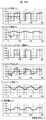
- FIG. 3 is an explanatory diagram showing changes in the electromagnetic coil voltage, current, freewheeling diode current, capacitor voltage, current, and power supply voltage for explaining the conduction noise of the electromagnetic coil drive control device shown in FIG. 1. is there. It is explanatory drawing which showed the noise spectrum for comparing with the drive control apparatus of the electromagnetic coil shown in FIG.
- reference numeral 1 is an electromagnetic coil drive control device targeted by the present invention, and a circuit element for controlling the current flowing through the electromagnetic coil 3 is provided therein.
- the electromagnetic coil 3 is used in various adjustment mechanisms.
- the electromagnetic coil of a hydraulic control valve used in the valve timing control device is shown.
- the hydraulic control valve is a control valve whose position linearly changes depending on the magnitude of current, and can control the position of the mover by an average current value that changes according to the on / off ratio (duty) of the drive current.
- this type of direct acting electric device is called a solenoid, and hence the electromagnetic coil 3 will be called a solenoid 3 hereinafter.
- circuit elements for driving the solenoid 3 are shown, and the description of other circuit elements is omitted.
- the electromagnetic coil drive control device 1 is provided with terminals T1, T2, and T3.
- the terminal T1 is connected to a DC power source 2, for example, a positive terminal of an in-vehicle battery, and the terminal T2 is connected to a negative terminal of the DC power source 2.
- the terminal T3 is connected to the positive terminal of the DC power source 2 through the solenoid 3.
- the solenoid 3 is a coil for constituting an electromagnet, and the position of the hydraulic control valve is changed by the current flowing through the solenoid 3, and the amount of oil in the hydraulic mechanism can be adjusted. This type of mechanism is well known and will not be described in detail here.
- the terminal T1 is connected to the positive electrode line L1 in the electromagnetic coil drive control device 1, and the terminal T2 is connected to the negative electrode line L5 in the electromagnetic coil drive control device 1.
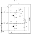
- the positive electrode line L1 and the negative electrode line L5 are connected by a connection line L3, and the impedance element 7 and the capacitor 6 are arranged and connected in series from the positive electrode line L1 to the negative electrode line L5 in the middle of the connection line L3.
- One end of the connection line L3 between the capacitor 6 and the impedance element 7 and the solenoid 3 is connected by a connection line L2, and a freewheeling diode 5 is disposed on the connection line L2.
- the cathode side of the return diode 5 is connected to a connection line L3 between the capacitor 6 and the impedance element 7, and the anode side of the return diode 5 is connected to one end of the solenoid 3.
- various capacitors including an electrolytic capacitor can be used as the capacitor 6, but a ceramic capacitor is used in this embodiment. This is because a ceramic capacitor has a small resistance value and is suitable for suppressing the generation of noise.
- connection line L4 the anode side of the reflux diode 5 and one end of the solenoid 3 and the negative line L5 are connected by a connection line L4, and a switching element 4 as a low-side switch is connected to the connection line L4.
- the switching element 4 is an FET, the drain side of the switching element 4 is connected between the anode side of the freewheeling diode 5 and one end of the solenoid 3, and the source side of the switching element 4 is connected to the negative electrode line L5.
- the positive side of the DC power supply 2 is connected to other circuits in the drive control device 1 of the electromagnetic coil via the positive line L1 and the GND side is connected to the other circuit in the electromagnetic coil drive control device 1 via the negative line L5. Since it is not related to the present invention, a detailed description is omitted.
- the switching element 4 when a predetermined control signal is given to the gate of the switching element 4, the switching element 4 is turned on, the drain voltage becomes 0V, and a current flows through the solenoid 3.
- the current flowing through the solenoid 3 is such that when the switching element 4 is in the ON state, the DC power source 2 and the solenoid 3 are in a closed circuit, and a drive current flows through the solenoid 3. This drive current increases with time, and electrical energy is stored in the inductance of the solenoid 3.
- the switching element 4 transitions to the OFF state, the solenoid 3, the freewheeling diode 5 and the impedance element 7 become a closed circuit and a free wheel current flows.
- the free wheel current flows so as to release the electrical energy stored in the inductance of the solenoid 3, and the current decreases with time.
- the freewheel current is a current that flows when the solenoid 3, the return diode 5, and the impedance element 7 are in a closed circuit when the switching element 4 is in the OFF state.
- the switching element 4 is in the ON state, the voltage on the anode side of the freewheeling diode 5 becomes 0V. As a result, the voltage on the cathode side becomes high, so that no freewheel current flows.
- FIG. 14 shows a conventional electromagnetic coil drive control device in which the impedance element 7 is not provided.
- the difference from the present embodiment is a portion surrounded by a rectangular dotted line.
- the conventional electromagnetic coil drive control device has a circuit configuration in which the connection point between the freewheeling diode 5 and the capacitor 6 is directly connected to the positive line L1 on the power supply side via the connection line L3. .
- the subject that the physique of the electronic control apparatus 1 became large as much as the capacity
- the ripple voltage can be suppressed by the impedance element 7 in this embodiment, the conduction noise can be efficiently suppressed and the capacity of the capacitor 6 can be reduced, so that the size of the electronic control device 1 can be reduced. become able to.
- 2A and 2B show the voltage of the DC power source 2 (in-vehicle battery is used in this embodiment), the inductance of the coil of the solenoid 3 is 15 mH, the resistance is 8 ⁇ , and the driving frequency of the switching element 4 is 10 kHz. In this example, the duty is 50%.
- FIG. 2A shows the conventional electromagnetic coil drive control device shown in FIG. 14 in which the capacity of the capacitor 6 is 220 ⁇ F
- FIG. 2B shows the electromagnetic coil drive control device shown in FIG.
- the impedance element 7 is a resistor having a resistance value of 6 ⁇ at 10 ⁇ F.
- the capacity of the capacitor 6 is 1/22.
- Solenoid voltage shown in FIGS. 2A and 2B The voltage of the solenoid 3 is a voltage on the drain side of the switching element 4. The on / off state when the driving frequency is 10 kHz and the duty is 50% is shown. When the switching element 4 is on, the drain voltage is about 0V and current flows through the solenoid 3, and when the switching element 4 is off, the drain voltage is about 14V and the current of the solenoid 3 is cut off.
- the solenoid current is a current on the drain side of the switching element 4.
- the DC power supply 2 and the solenoid 3 become a closed circuit, and a drive current flows through the solenoid 3.
- This drive current increases with time, and electrical energy is stored in the inductance of the solenoid 3.
- the solenoid 3 the return diode 5 and the impedance element 7 become a closed circuit, and free wheel current flows.
- the electric current stored in the inductance of the solenoid 3 is discharged, and the current decreases with time. Since the conventional electromagnetic coil drive control device does not include the impedance element 7, the charge of the capacitor 6 is not consumed as will be described later.
- the capacitor current is about 0.4 A
- the time is about 50 ⁇ s
- the capacitance is 220 ⁇ F
- the capacitor current is about 0.4 A
- the time is about 50 ⁇ s
- the capacitance is 10 ⁇ F
- the power supply voltage is the voltage of the positive line L1 or the terminal T1.
- the magnitude of the ripple voltage of the power source is obtained from the difference between the maximum voltage and the minimum voltage, and in this example is as small as several hundred mV.
- This is a circuit configuration in which the electric charge of the capacitor 6 is directly transmitted to the positive electrode line L1, but the voltage fluctuation is small because the capacitance of the capacitor 6 is set to be as large as 220 ⁇ F.
- the physique of the electromagnetic coil drive control device is increased, which is not preferable.
- the ripple voltage of the power source is as small as several hundred mV in the electromagnetic coil drive control device according to this embodiment of FIG. 2B.
- the reason for this is that even if the capacitance of the capacitor 6 is considerably reduced, since the impedance element 7 is disposed between the capacitor 6 and the positive electrode line L1, the voltage generated in the capacitor 6 (in this case, about 2.5V) This is because they are consumed by the impedance element 7 and thus do not appear on the positive line L1.
- the physique of the drive control apparatus of an electromagnetic coil can be made small.
- the impedance of the wiring between the DC power supply 2 and the impedance element 7 is 0 ⁇ , the voltage at the terminal T1 is fixed at 14V and the ripple voltage of the power supply becomes 0V.
- there is a slight impedance because there is a wiring inductance or a wiring resistance between the DC power source 2 and the impedance element 7.
- a voltage corresponding to the wiring impedance and the voltage dividing ratio of the impedance element 7 is observed at the terminal T1.
- the inductance of the wiring is 10 ⁇ H
- the wiring impedance (reactance) is about 0.6 ⁇ .
- the conventional electromagnetic coil drive control device has a configuration in which conduction noise is suppressed by the large-capacitance capacitor 6, and the conduction noise can be suppressed. There was a problem that the physique of became large.
- conduction noise is sufficiently suppressed by using the impedance element 7 and the capacitor 6, and the capacitance of the capacitor 6 can be considerably reduced. Can be reduced.
- CISPR25 “Interference wave limit value and measurement method for in-vehicle receiver protection” prepared by the International Radio Interference Special Committee (CISPR).
- the CISPR25 standard relates to radio interference in the frequency band of 150 kHz to 1,000 MHz and is applied to electronic components used in automobiles. The recommended value is determined to protect the receiver in the same car from the interference generated from the parts and modules in the car.
- the receivers to be protected are radio, television and radio equipment. is there.
- the noise spectrum of the example shown in FIG. 1 and the conventional example shown in FIG. 14 was measured.
- This noise spectrum is noise derived from the voltage of the power supply line between the terminal T1 and the DC power supply 2.
- the frequency ranged from 100 kHz to 500 kHz.
- the capacitance of the capacitor 6 is set to 220 ⁇ F, and in the present embodiment shown in FIG. 1, the capacitance of the capacitor 6 is set to 10 ⁇ F, the impedance element 7 is a resistor, and the resistance value is set to 6 ⁇ . .
- the noise level at a measurement frequency of 100 kHz is 69 dB ⁇ V in the conventional example (in the broken line (illustrated)) and 64 dB ⁇ V in the present example (in the solid line (illustrated)). Further, the noise level increases as the measured frequency increases. Although it becomes smaller, it can be understood that the noise level is always kept small in this embodiment as compared with the conventional example.
- the noise suppression effect is further promoted as indicated by the solid line, and the noise is reduced compared to the conventional example. You can see that the level is small.
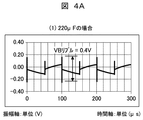
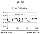
- FIG. 4A shows the magnitude of the ripple voltage of the conventional example shown in FIG. 14, and FIG. 4B shows the magnitude of the ripple voltage of this embodiment shown in FIG.
- the ripple voltage is reduced to 0.2 V, the magnitude of the ripple voltage is about half, and the noise level It can be seen that is effectively suppressed.
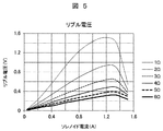
- FIG. 5 shows the relationship between the drive current flowing through the solenoid 3 and the ripple voltage with respect to the resistance value of the impedance element 7.
- this ripple voltage is observed as a voltage corresponding to the wiring impedance from the DC power supply 2 and the voltage dividing ratio of the impedance element 7. Therefore, it can be seen that the larger the value of the impedance element 7 is, the larger the voltage division ratio becomes, so that the ripple voltage becomes smaller.
- FIG. 6 shows the relationship between the drive current of the solenoid 3 and the loss of the impedance element 7 with respect to the resistance value of the impedance element 7. According to the present embodiment, it can be seen that the greater the resistance value of the impedance element 7, the greater the loss. Since the loss is caused by the impedance element 7 and the current flowing therethrough, it can be understood that if the solenoid current is the same, the loss is proportional to the resistance value of the impedance element 7.
- the ripple voltage and the loss of the impedance element 7 are in a contradictory relationship. That is, from the viewpoint of reducing conduction noise, it is desirable to increase the resistance of the impedance element 7, but from the viewpoint of loss, it is desirable to decrease the resistance of the impedance element 7. Therefore, the range of the value of the impedance element 7 is naturally determined from the allowable range of the ripple voltage and the allowable range of the loss of the impedance element 7. For example, when the maximum ripple voltage is 0.4 V or less and the loss of the impedance element is allowed up to 0.7 W, the resistance value of 6 ⁇ is selected, and the maximum ripple voltage is 1.4 V or less and the loss of the impedance element is 0. If up to 4W is allowed, 2 ⁇ should be selected.
- the resistance value of the impedance element 7 may be appropriately selected from the relationship between the ripple voltage and the loss according to the specification of the drive control device of the applied electromagnetic coil, and in short, the conduction noise is efficiently reduced.
- a resistance value that can reduce loss can be selected.
- the impedance element 7 has been described as a resistor, as shown in FIGS. 7A to 7F, a passive element other than a resistor, an active element, or a combination with a resistor may be used.
- a specific configuration of the impedance element 7 will be described with reference to FIGS. 7A to 7F.
- 7A to 7F propose a configuration in which a resistor is used as a basic configuration and other impedance elements are combined with this in order to efficiently reduce noise.
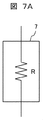
- FIG. 7A shows an example in which a single resistor is used as the impedance element 7.
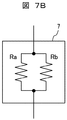
- FIG. 7B shows an example in which two resistors are used in parallel as the impedance element 7.
- the loss of the impedance element 7 is proportional to the square of the flowing current. Therefore, by dispersing the resistor Ra and the resistor Rb, it is effective to reduce the loss of each resistor by half.
- FIG. 7C shows an example in which the impedance element 7 includes a plurality of (here, two) resistors and a plurality of resistance adjusting elements for selecting them, that is, switching elements.
- the resistor Rx and the resistor Ry desirably have different resistance values. By doing so, a plurality of selections can be made by a combination of ON / OFF of the switch SWx and the switch SWy. For example, if one resistance value is increased and the other resistance value is decreased, conduction noise can be further suppressed when one resistance value is selected, and loss is further reduced when the other resistance value is selected. be able to.
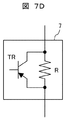
- FIG. 7D shows an example in which a resistor is connected in parallel between the collector and the emitter of the bipolar transistor TR having the function of a resistance adjusting element as the impedance element 7.
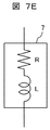
- FIG. 7E shows an example in which a resistor R and an inductance L are combined in series as the impedance element 7. This is effective when it is desired to further increase the impedance of the frequency in the high frequency band, that is, to further suppress high-frequency conduction noise.
- FIG. 7F shows an example in which a parallel resonant circuit of a resistor R, an inductance L, and a capacitor C is connected in series as the impedance element 7. This is effective when it is desired to increase impedance at a specific frequency, that is, to suppress specific conduction noise more.
- the impedance element 7 as shown in FIGS. 7E and 7F it is extremely easy to appropriately combine a resistor, an inductance, and a capacitor.
- An inductance or a capacitor is suitable as an impedance element because there is no loss.
- the impedance element 7 and the capacitor 6 are connected from the positive line L1 to the negative line L5 to the connection line L3 connecting the positive line L1 and the negative line L5 of the DC power supply.
- the anode side and one end of the solenoid 3 and the negative electrode line L3 are connected by a low-side switching element 4.
- the conduction noise caused by the drive current of the solenoid 3 can be suppressed by the impedance element 7, and the capacitance of the capacitor 6 can be further reduced. Therefore, the drive control device for the electromagnetic coil can be downsized. Is.
- the second embodiment uses two solenoids 3 and shows, for example, an electromagnetic coil of a hydraulic control valve used for each of an intake valve and an exhaust valve used in a valve timing control device.
- the embodiment shown in FIG. 8 is characterized in that two drive circuits shown in FIG. 1 are provided and the impedance element 7 and the capacitor 6 are commonly connected to the two drive circuits. Since the functions of the impedance element 7 and the capacitor 6 are substantially the same as those of the impedance element 7 and the capacitor 6 shown in FIG. 1, detailed description thereof will be omitted and the circuit configuration will be described.
- One drive circuit is composed of a solenoid 3a, a connection line L2a, a switching element 4a, and a reflux diode 5a
- the other drive circuit is composed of a solenoid 3n, a connection line L2n, a switching element 4n, and a reflux diode 5n.
- These basic connections are substantially the same as the circuit shown in FIG.
- the cathodes of the free-wheeling diode 5a and the free-wheeling diode 5n are connected to a connection line L3 between the impedance element 7 and the capacitor 6. According to this configuration, only one impedance element 7 and one capacitor 6 are required, which is effective in reducing the number of components. In this case, it is necessary that the capacitance of the capacitor 6 and the resistance value of the impedance element 7 be adapted to values according to the two drive circuits.
- FIG. 9 shows a modification of the embodiment shown in FIG. 8, and includes two drive circuits shown in FIG. 1, and an impedance element and a capacitor are also provided in each drive circuit correspondingly. It is what. Also in this embodiment, the functions of the impedance element 7 and the capacitor 6 are substantially the same as those of the impedance element 7 and the capacitor 6 shown in FIG.
- One drive circuit is composed of a solenoid 3a, a connection line L2a, a switching element 4a, and a reflux diode 5a
- the other drive circuit is composed of a solenoid 3n, a connection line L2n, a switching element 4n, and a reflux diode 5n.
- the cathode of the return diode 5a is connected to the line L3a together with the impedance element 7a and the capacitor 6a
- the cathode of the return diode 5n is connected to the line L3n together with the impedance element 7n and the capacitor 6n.
- the impedance elements 7a and 7n and the capacitors 6a and 6n exist independently in each of the two drive circuits, it is particularly effective for reducing the loss of the impedance element 7.
- the impedance element 7 since the impedance element 7 is commonly used for the two drive circuits, the resistance value thereof increases, and there is a possibility that the loss increases as shown in FIG.
- the impedance elements 7a and 7n are provided in the respective drive circuits, the resistance value can be reduced, so that the loss can be reduced.
- the impedance element 7 has been described as a resistor, an impedance element having a configuration as shown in FIGS. 7A to 7F can also be used.
- the capacitor 6 and the impedance element 7 can be arranged even in the drive circuit of the plurality of solenoids 3, the conduction noise is reduced.
- the capacitance of the capacitor By reducing the capacitance of the capacitor, the size of the electromagnetic coil drive control device can be reduced.
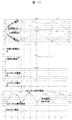
- FIG. 10 shows the timing at which the two drive circuits change simultaneously.
- the switching element 4a and the switching element 4n of the two drive circuits are turned off (illustration: circuit 1 off, circuit 2 off)
- the freewheeling diode 5a and the freewheeling diode 5n are forward biased (circuit 1 current (reflux)).
- the solenoid current recirculates (illustration: solenoid current 1, solenoid current 2)
- the voltage across the capacitor 6 increases with time (illustration: voltage across the capacitor).
- the current flowing through the impedance element 7n also rises and the point at which the switching element transitions from OFF to ON becomes the maximum current (illustration: impedance element current). Since the solenoid current from the two drive circuits circulates in the impedance element 7n, the current is about twice as large, and the loss increases from the square of R ⁇ I to about four times that in the case of one drive circuit. . According to the analysis result, it can be seen that the average loss is as large as about 1160 mW (illustration: impedance element loss).
- FIG. 11 shows a case where the phases of PWM drive of the two drive circuits are shifted by a half cycle.
- the switching element 4n is turned off (illustration: circuit 2 off)
- the freewheeling diode 5n is forward biased and the solenoid current recirculates (illustration: solenoid 2 current).
- the switching element 4a is in an on state (illustration: circuit 1 is on), the freewheeling diode 5n is reverse-biased and does not recirculate (illustration: solenoid 1 current).
- the VB ripple voltage shown in FIG. 10 (illustration: ripple voltage) and the VB ripple voltage shown in FIG. 11 (illustration: ripple voltage)
- the VB ripple voltage is greatly increased by shifting the PWM phase. The effect that it can be reduced can be seen.
- FIG. 15 shows the timing at which the two drive circuits change simultaneously.
- the switching element 4a of the two drive circuits is turned off (illustration: circuit 1 off)
- the freewheeling diode 5a becomes forward biased
- the solenoid current recirculates (illustration: solenoid 1 current)
- both ends of the capacitor 6a The voltage rises with time (illustration: voltage across the capacitor).
- the current flowing through the impedance element 7a also increases (illustration: impedance element current), and the point at which the switching element transitions from OFF to ON is the maximum current.
- the switching element 4n When the switching element 4n is turned off (illustration: circuit 2 off), the freewheeling diode 5n becomes forward biased, the solenoid current recirculates (illustration: solenoid 2 current), and the voltage across the capacitor 6n increases with time. (Figure: Voltage across capacitor). Then, it can be seen that the current flowing through the impedance element 7n also increases (illustration: impedance element current), and the point at which the switching element transitions from OFF to ON is the maximum current. According to the result of the analysis tool, it can be seen that the average loss is about 330 mW (illustration: impedance element loss).
- FIG. 16 shows a case where the phases of PWM drive of the two drive circuits are shifted by a half cycle.
- the switching element 4n is turned off (illustration: circuit 2 off)
- the freewheeling diode 5n is forward biased and the solenoid current recirculates (illustration: solenoid 2 current).
- the switching element 4a is in an on state (illustration: circuit 1 is on), the freewheeling diode 5n is reverse-biased and does not recirculate (illustration: solenoid 1 current).
- the point at which the switching element transitions from off to on is the maximum current (illustration: impedance element current).
- the average loss is 320 mW (illustration: impedance element loss).
- the VB ripple voltage (illustrated: ripple voltage) shown in FIG. 15 and the VB ripple voltage (illustrated: ripple voltage) shown in FIG. 16, the VB ripple voltage is also greatly reduced by shifting the phase of the PWM. You can see the effect of being able to do it.
- FIG. 12 and FIG. 13 show timing waveforms and block configurations when a timer module of a microcomputer is used, and an embodiment will be described.
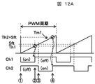
- FIG. 12 shows a control method in which the timing is shifted by a predetermined phase difference.
- FIG. 12A is a timing diagram
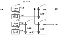
- FIG. 12B shows the block configuration and describes the flow of operation.
- the threshold register 12a is a PWM on-time setting value of the driving circuit 1
- the threshold register 12b is a PWM on-time setting value of the driving circuit 2
- the shift value register 14 is a phase difference (timing shift) time of the driving circuit 2.
- a setting value, and a half cycle of the PWM frequency will be described as an example of the setting value.
- this is a control method in which the timing is shifted by a predetermined phase difference.
- the phase difference has been described with a half cycle (PWM cycle / 2) when there are two drive circuits.
- PWM cycle / 2 when the number of drive circuits is increased, for example, three circuits are PWM cycles / 3, and four circuits are PWMs. Needless to say, the period / 4 is effective.
- FIG. 13 shows a control method in which the timing is shifted by starting the other timer using an end event of one timer as a trigger.
- FIG. 13A is a timing diagram, and the configuration is shown in FIG. 13B and the flow of operation will be described.
- the threshold register 12 a is a PWM on-time setting value of the drive circuit 1
- the threshold register 12 b is a PWM on-time setting value of the drive circuit 2.
- Ch2 becomes 0 and the drive circuit 2 is turned on (this time is the maximum current of the drive circuit 1 and the minimum current of the drive circuit 2).
- Ch the count permission EN of the fixed-cycle timer 11b is enabled, and the reference clock Clk is input to start counting up one by one.
- this is a control method in which the timing is shifted by starting the other timer using the end event of one timer as a trigger.
- the sum of the ON times of the two drive circuits must not exceed the PWM period (when the number of drive circuits is increased, for example, the same applies to three circuits and four circuits).
- SYMBOLS 1 Drive control apparatus of an electromagnetic coil, 2 ... DC power supply, 3, 3a, 3n ... Electromagnetic coil (solenoid) 4, 4a, 4n ... Switching element 5, 5a, 5n ... Freewheeling diode, 6, 6a, 6n ... Capacitors 7, 7a, 7n ... impedance elements, L1 ... positive line, L2, L3, L4 ... connection line, L5 ... negative line, L2a, L2n, L3a, L3n, L4a, L4n ... connection line. 11a, 11b ... fixed-cycle timer, 12a, 12b ... threshold register, 13a, 13b ... comparator, 14 ... shift value register, 15 ... adder
Landscapes
- Physics & Mathematics (AREA)
- Electromagnetism (AREA)
- Engineering & Computer Science (AREA)
- Power Engineering (AREA)
- Electronic Switches (AREA)
- Power Conversion In General (AREA)
Abstract
コンデンサの容量を低減しつつ、伝導ノイズを効率的に抑制することができる電磁コイルの駆動制御装置を提供することにある。直流電源の正極ラインと負極ラインを接続する接続ラインにコンデンサとインピーダンス素子を直列に配置し、コンデンサとインピーダンス素子の間の接続ラインと電磁コイルの一端とを還流ダイオードを介して接続し、更に還流ダイオードと電磁コイルの一端の間と正極ライン、或いは負極ラインの間をスイッチング素子で接続した。インピーダンス素子によって電磁コイルの駆動電流に起因した伝導ノイズを抑制でき、更にコンデンサの容量を小さくできるために、電磁コイルの駆動制御装置を小型化することが可能となる。さらに、スイッチング素子の駆動タイミングを制御することによって、インピーダンス素子の損失低減とリプル電圧低減が可能となる。
Description
本発明は電磁石を用いた調節機構や電動機に使用される電磁コイルの駆動制御装置に係り、特に直流電源から電力を供給される電磁コイルの駆動制御装置に関するものである。
例えば、自動車等においては、環境問題、排気ガス排出規制への対応はもとより、省エネルギー意識の高まりや資源枯渇の懸念から内燃機関の燃費(燃料消費量)を改善することが要請されている。そして、このためには内燃機関の燃焼効率を高めることによって少ない燃料で燃焼を行い、更に排気有害成分を低減するようにしている。
内燃機関の燃焼効率を高める例として、内燃機関の回転数や吸入空気量(負荷)に基づいて吸気バルブや排気バルブの開閉タイミングを最適化するバルブタイミング制御装置(VTC:Valve Timing Control)が知られている。このバルブタイミング制御装置はカムシャフトを相対的に回転させる油圧機構を備え、電磁石を使用した油圧制御弁の開度を制御することで油圧機構の油量を調整して吸気バルブや排気バルブの開閉タイミングを変えるようにしたものである。
このバルブタイミング制御装置の他にも、燃費を改善するために自動変速機に使用される変速制御弁や吸気通路に設けた電子スロットル制御装置等が使用されている。これらは電磁石や電動機を主たる駆動源としており、これらは電磁コイルに供給される電力によって駆動、制御されている。このように、自動車の機構部を操作するためには電磁石や電動機の電磁コイルに流れる電力を制御する電磁コイルの駆動制御装置が必須の構成となっている。
例えば、電磁コイルを駆動するための駆動制御装置としては、特開2006-35190号公報(特許文献1)にあるように、電磁コイルにローサイドスイッチを設け、このスイッチを開閉することで電磁コイルに流れる電流等を制御するようにしている。この特許文献1にいては電磁コイルの温度上昇を抑える目的で電磁コイルに発生する誘導電流の減衰時間を短くする方法が記載されている。
ところで、電磁コイルを駆動、制御する電磁コイルの駆動制御装置において、電磁コイルに流れる電流をオン/オフして電磁コイルを励起状態、或いは非励起状態に駆動する際に、直流電源の正極に繋がれたケーブルや基板パターン等の配線に電磁コイルに流れる電流のオン/オフに起因する伝導ノイズが発生するという現象がある。
従来の技術においては、大容量のコンデンサを配線に配置することで伝導ノイズを吸収する手法が一般的であった。しかしながら、近年、電磁コイルの駆動制御装置の小型化等の理由から大容量のコンデンサを小型化すると共に、伝導ノイズを効率的に抑制したいとの要請が強くなされてきている。
本発明の目的は、このような要請に応えるため、コンデンサの容量を低減しつつ、伝導ノイズを効率的に抑制することができる電磁コイルの駆動制御装置を提供することにある。
本発明の特徴は、直流電源の正極ラインと負極ラインとを接続する接続ラインにコンデンサとインピーダンス素子を直列に配置し、コンデンサとインピーダンス素子の間の接続ラインと直流電源の正極側に繋がれた電磁コイルの反対側の端部を還流ダイオードを介して接続し、更に還流ダイオードと電磁コイルの端部の間の接続線と正極ライン、或いは負極ラインの間をスイッチング素子を有した接続線で接続した、ところにある。ここで、スイッチング素子が正極ラインと接続された場合はハイサイドスイッチとなり、負極ラインと接続された場合はローサイドスイッチとなる。
本発明によれば、インピーダンス素子によって電磁コイルの駆動電流に起因した伝導ノイズを抑制でき、更にコンデンサの容量を小さくできるために、電磁コイルの駆動制御装置を小型化することが可能となる。
以下、本発明の実施形態について図面を用いて詳細に説明するが、本発明は以下の実施形態に限定されることなく、本発明の技術的な概念の中で種々の変形例や応用例をもその範囲に含むものである。
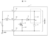
本発明の第1の実施形態について図1に基づき詳細に説明する。図1において、参照番号1は本発明が対象とする電磁コイルの駆動制御装置であって、内部に電磁コイル3に流れる電流を制御する回路素子が設けられている。電磁コイル3は種々の調整機構に用いられるが、本実施例においてはバルブタイミング制御装置に使用される油圧制御弁の電磁コイルを示している。油圧制御弁は電流の大きさによって位置が線形的に変わる制御弁であり、駆動電流のオン/オフ比率(デューティ)に応じて変化する平均電流値によって可動子の位置を制御できるものである。一般にこの種の直動式電気機器はソレノイドと呼ばれているので、以下、電磁コイル3をソレノイド3と称することにする。尚、この図においては、ソレノイド3を駆動する回路素子を示し、これ以外の回路素子は説明を省略している。
電磁コイルの駆動制御装置1には端子T1、T2、T3が設けられており、端子T1は直流電源2、例えば車載バッテリの正極端子と接続され、端子T2は直流電源2の負極端子と接続され、端子T3はソレノイド3を介して直流電源2の正極端子と接続されている。このソレノイド3が電磁石を構成するためのコイルであり、このソレノイド3に流れる電流によって油圧制御弁の位置が変わり、油圧機構の油量を調整することができるものである。この種の機構は良く知られているので、ここでは詳細な説明は省略する。
端子T1は電磁コイルの駆動制御装置1内で正極ラインL1と接続され、端子T2は電磁コイルの駆動制御装置1内で負極ラインL5と接続されている。正極ラインL1と負極ラインL5は接続ラインL3によって接続されており、この接続ラインL3の途中に正極ラインL1から負極ラインL5に向かってインピーダンス素子7とコンデンサ6とが直列に配置、接続されている。コンデンサ6とインピーダンス素子7の間の接続ラインL3とソレノイド3の一端は接続ラインL2によって接続され、この接続ラインL2には還流ダイオード5が配置されている。還流ダイオード5のカソード側はコンデンサ6とインピーダンス素子7の間の接続ラインL3に接続され、還流ダイオード5のアノード側はソレノイド3の一端と接続されている。
ここで、コンデンサ6は電解コンデンサ等を含め種々のコンデンサを使用することができるが、本実施例ではセラミックコンデンサを使用している。セラミックコンデンサの場合は抵抗値が小さいので、ノイズの発生を抑制するのに適しているからである。
更に、還流ダイオード5のアノード側とソレノイド3の一端の間と、負極ラインL5とは接続ラインL4によって接続され、この接続ラインL4にはローサイドスイッチとしてのスイッチング素子4が接続されている。このスイッチング素子4はFETであり、スイッチング素子4のドレイン側は還流ダイオード5のアノード側とソレノイド3の一端の間に接続され、スイッチング素子4のソース側は負極ラインL5と接続されている。
尚、直流電源2の正極側は正極ラインL1を介して、またGND側は負極ラインL5を介して電磁コイルの駆動制御装置1内の他の回路へ接続されて電力を供給するが、ここでは本発明に関係しないので詳細な説明は省略する。
以上において、所定の制御信号がスイッチング素子4のゲートに与えられると、スイッチング素子4がオン状態に遷移し、ドレイン電圧は0Vになってソレノイド3に電流が流れる。ソレノイド3に流れる電流は、スイッチング素子4がオン状態の時に直流電源2とソレノイド3が閉回路になってソレノイド3に駆動電流が流れるものである。この駆動電流は時間経過とともに増加し、ソレノイド3のインダクタンスに電気的なエネルギーが蓄積される。
一方、スイッチング素子4がオフ状態に遷移した時には、ソレノイド3、還流ダイオード5及びインピーダンス素子7が閉回路となってフリーホイール電流が流れる。フリーホイール電流はソレノイド3のインダクタンスに蓄えられた電気的なエネルギーを放出するように流れ、電流は時間経過とともに減少する。フリーホイール電流は、スイッチング素子4がオフ状態の時に、ソレノイド3、還流ダイオード5、インピーダンス素子7が閉回路になって流れる電流である。スイッチング素子4がオン状態の時には還流ダイオード5のアノード側の電圧が0Vになるために、この結果、カソード側の電圧が高くなることでフリーホイール電流は流れないものである。
また、これに加えてスイッチング素子4がオフ状態の時に、直流電源2、ソレノイド3、還流ダイオード5とコンデンサ6が閉回路になって、コンデンサ6に電荷が蓄えられる。逆にスイッチング素子4がオン状態の時には、還流ダイオード5に電流が流れないので、スイッチング素子4がオフ状態の時にコンデンサ6に蓄えられた電荷は、インピーダンス素子7に向かって流れ出るようになる。このコンデンサ6に蓄えられた電荷は正極ラインL1に加えられることになるが、本実施例ではコンデンサ6と正極ラインL1の間にインピーダンス素子7が配置されているので、コンデンサ6蓄えられた電荷はインピーダンス素子7によって消費されて、正極ラインL1に重畳されないようになる。これによって、正極ラインL1にはリプル電圧が発生するのが抑制され、伝導ノイズが低減できるようになるものである。このリプル電圧はソレノイド3のオン/オフに対応した高周波の伝導ノイズである。
本実施例と比較するため、図14にインピーダンス素子7を設けていない従来の電磁コイルの駆動制御装置を示している。図14からわかるように、本実施例と比較して異なるのは四角形の点線で囲まれた部分である。従来の電磁コイルの駆動制御装置では図14に示すように、還流ダイオード5とコンデンサ6の接続点が接続ラインL3を介して電源側の正極ラインL1と直接的に接続される回路構成であった。このため、リプル電圧を抑制するためにはコンデンサ6の容量を大きくする必要があった。したがって、コンデンサ6の容量が大きくなる分だけ電子制御装1の体格が大きくなるという課題が生じていた。
一方、本実施例においてはインピーダンス素子7によってリプル電圧を抑制できるようになるので、効率的に伝導ノイズを抑制し、かつコンデンサ6の容量を小さくできるので電子制御装1の体格を小さくすることができるようになる。
次に、図1に示す第1の実施形態になる電磁コイルの駆動制御装置と図14に示す従来の電磁コイルの駆動制御装置の動作を比較して説明することとする。図2A、図2Bは、直流電源2(本実施例では車載バッテリを用いている)の電圧が14V、ソレノイド3のコイルのインダクタンスが15mHでその抵抗値が8Ω、スイッチング素子4の駆動周波数が10kHzでデューティ=50%とした場合の例である。
図2Aは図14に示した従来の電磁コイルの駆動制御装置で、コンデンサ6の容量は220μFの場合を示し、図2Bは図1に記載の電磁コイルの駆動制御装置で、コンデンサ6の容量は10μFでインピーダンス素子7が6Ωの抵抗値を有する抵抗とした場合の例である。このように本実施例ではコンデンサ6の容量を1/22としている。以下、各回路素子の電流や電圧の挙動を説明する。
(1)図2A、図2Bに示すソレノイド電圧
ソレノイド3の電圧は、スイッチング素子4のドレイン側の電圧である。駆動周波数10kHz、デューティ=50%とした場合のオン/オフ状態を示している。スイッチング素子4がオン状態である時、ドレイン電圧は約0Vになってソレノイド3に電流が流れ、スイッチング素子4がオフ状態である時、ドレイン電圧は約14Vになってソレノイド3の電流が遮断される。
ソレノイド3の電圧は、スイッチング素子4のドレイン側の電圧である。駆動周波数10kHz、デューティ=50%とした場合のオン/オフ状態を示している。スイッチング素子4がオン状態である時、ドレイン電圧は約0Vになってソレノイド3に電流が流れ、スイッチング素子4がオフ状態である時、ドレイン電圧は約14Vになってソレノイド3の電流が遮断される。
(2)図2A、図2Bに示すソレノイド電流
ソレノイド電流は、スイッチング素子4のドレイン側の電流である。スイッチング素子4がオン状態の時に直流電源2とソレノイド3が閉回路になってソレノイド3に駆動電流が流れる。この駆動電流は時間経過とともに増加し、ソレノイド3のインダクタンスに電気的なエネルギーが蓄積される。また、スイッチング素子4がオフ状態の時にはソレノイド3と還流ダイオード5とインピーダンス素子7が閉回路となってフリーホイール電流が流れる。ソレノイド3のインダクタンスに蓄えられた電気的なエネルギーを放出するよう流れ、電流は時間経過とともに減少する。尚、従来の電磁コイルの駆動制御装置ではインピーダンス素子7が備えられていないので、後述するようにコンデンサ6の電荷の消費は行われない。
ソレノイド電流は、スイッチング素子4のドレイン側の電流である。スイッチング素子4がオン状態の時に直流電源2とソレノイド3が閉回路になってソレノイド3に駆動電流が流れる。この駆動電流は時間経過とともに増加し、ソレノイド3のインダクタンスに電気的なエネルギーが蓄積される。また、スイッチング素子4がオフ状態の時にはソレノイド3と還流ダイオード5とインピーダンス素子7が閉回路となってフリーホイール電流が流れる。ソレノイド3のインダクタンスに蓄えられた電気的なエネルギーを放出するよう流れ、電流は時間経過とともに減少する。尚、従来の電磁コイルの駆動制御装置ではインピーダンス素子7が備えられていないので、後述するようにコンデンサ6の電荷の消費は行われない。
(3)図2A、図2Bに示すフリーホイール電流
フリーホイール電流は、スイッチング素子4がオフ状態の時に、ソレノイド3、還流ダイオード5及びインピーダンス素子7が閉回路になって流れる電流であり、図では還流ダイオード5のカソード側の電流を示している。スイッチング素子4がオン状態の時には還流ダイオード5のアノード電圧が0Vになるために、カソード電圧が高くなるので流れないようになる。この場合も、従来の電磁コイルの駆動制御装置ではインピーダンス素子7が備えられていないので、後述するようにコンデンサ6の電荷の消費は行われない。
フリーホイール電流は、スイッチング素子4がオフ状態の時に、ソレノイド3、還流ダイオード5及びインピーダンス素子7が閉回路になって流れる電流であり、図では還流ダイオード5のカソード側の電流を示している。スイッチング素子4がオン状態の時には還流ダイオード5のアノード電圧が0Vになるために、カソード電圧が高くなるので流れないようになる。この場合も、従来の電磁コイルの駆動制御装置ではインピーダンス素子7が備えられていないので、後述するようにコンデンサ6の電荷の消費は行われない。
(4)図2A、図2Bに示すコンデンサ電流
スイッチング素子4がオフ状態の時に、直流電源2とソレノイド3、還流ダイオード5、コンデンサ6が閉回路になって、コンデンサ6に電荷が蓄えられる。スイッチング素子4がオン状態の時には還流ダイオード5に電流が流れないので、それまでに蓄えられた電荷はインピーダンス素子7に向かって流れ出るようになる。図ではコンデンサ6と、接続線L2と接続線L3の接続点(VCで(図示:)の間の電流を示している。従来の電磁コイルの駆動制御装置ではインピーダンス素子7が備えられていないので、正極ラインL1に向かってコンデンサ6の電荷は流れ出るようになる。
スイッチング素子4がオフ状態の時に、直流電源2とソレノイド3、還流ダイオード5、コンデンサ6が閉回路になって、コンデンサ6に電荷が蓄えられる。スイッチング素子4がオン状態の時には還流ダイオード5に電流が流れないので、それまでに蓄えられた電荷はインピーダンス素子7に向かって流れ出るようになる。図ではコンデンサ6と、接続線L2と接続線L3の接続点(VCで(図示:)の間の電流を示している。従来の電磁コイルの駆動制御装置ではインピーダンス素子7が備えられていないので、正極ラインL1に向かってコンデンサ6の電荷は流れ出るようになる。
(5)図2A、図2Bに示すコンデンサ電圧
コンデンサ6の電圧(VC点)は、定常時は直流電源2の14Vであり、コンデンサ電流によって変動した電圧分だけ重畳する。図では接続線L2と接続線L3の接続点(VCで(図示:)の電圧である。この電圧は一般にはQ=ITとQ=CVより、V=IT/Cで求められて、電流に比例し、容量に反比例することがわかる。ここで、Qは電荷、Cは容量、Vは電極間の電圧、Iは電極間を流れる電流、Tは時間である。
コンデンサ6の電圧(VC点)は、定常時は直流電源2の14Vであり、コンデンサ電流によって変動した電圧分だけ重畳する。図では接続線L2と接続線L3の接続点(VCで(図示:)の電圧である。この電圧は一般にはQ=ITとQ=CVより、V=IT/Cで求められて、電流に比例し、容量に反比例することがわかる。ここで、Qは電荷、Cは容量、Vは電極間の電圧、Iは電極間を流れる電流、Tは時間である。
図2Aに示す従来の電磁コイルの駆動制御装置では、コンデンサ電流が約0.4A、時間は約50μs、静電容量が220μFより、コンデンサ電圧は、
V=14+0.4×50/220=14+0.1=14.1(V)
となる。
V=14+0.4×50/220=14+0.1=14.1(V)
となる。
図2B示す本実施例になる電磁コイルの駆動制御装置では、コンデンサ電流が約0.4A、時間は約50μs、静電容量が10μFより、コンデンサ電圧は、
V=14+0.4×50/10=14+2.5V=16.5(V)
となる。
V=14+0.4×50/10=14+2.5V=16.5(V)
となる。
(6)図2A、図2Bに示す電源電圧
電源電圧は正極ラインL1或いは端子T1の電圧である。図2Aの従来の電磁コイルの駆動制御装置では、電源のリプル電圧の大きさは最大電圧と最低電圧の差から求められ、この例では数百mV程度と小さい。これは、コンデンサ6の電荷が正極ラインL1に直接伝わる回路構成であるが、コンデンサ6の容量が220μFと大きく設定されていることから電圧変動が少ないものである。しかしながら、このように、コンデンサ6を大きくすると電磁コイルの駆動制御装置の体格が大きくなり、好ましいものではなかった。
電源電圧は正極ラインL1或いは端子T1の電圧である。図2Aの従来の電磁コイルの駆動制御装置では、電源のリプル電圧の大きさは最大電圧と最低電圧の差から求められ、この例では数百mV程度と小さい。これは、コンデンサ6の電荷が正極ラインL1に直接伝わる回路構成であるが、コンデンサ6の容量が220μFと大きく設定されていることから電圧変動が少ないものである。しかしながら、このように、コンデンサ6を大きくすると電磁コイルの駆動制御装置の体格が大きくなり、好ましいものではなかった。
一方、図2Bの本実施例になる電磁コイルの駆動制御装置においても電源のリプル電圧が数百mV程度と小さいことがわかる。この理由は、コンデンサ6の容量をかなり小さくしても、インピーダンス素子7がコンデンサ6と正極ラインL1との間に配置されているため、コンデンサ6で発生した電圧(この場合は2.5V程度)はインピーダンス素子7によって消費されるために正極ラインL1には現れないからである。このため、伝導ノイズを抑制すると共に、コンデンサ6の容量を小さくできるので、電磁コイルの駆動制御装置の体格を小さくできるようになる。
仮に、直流電源2からインピーダンス素子7までの間の配線などのインピーダンスが0Ωである場合は、端子T1の電圧は14Vに固定され、電源のリプル電圧は0Vになる。しかしながら、実際には、直流電源2からインピーダンス素子7までの間に配線インダクタンスや配線抵抗があるため、若干のインピーダンスが存在することになる。その場合、端子T1には、その配線インピーダンスとインピーダンス素子7の分圧比に相当する電圧が観測される。例えば、配線のインダクタンスを10μHと仮定すると、配線インピーダンス(リアクタンス)は、約0.6Ωである。インピーダンス素子7が6Ω、コンデンサ6の電圧が2.5V変動した場合のリプル電圧は、V=2.5×0.6/(0.6+6)=0.2Vとなり、十分小さくすることができる。
以上、説明したように、従来の電磁コイルの駆動制御装置においては大容量のコンデンサ6によって伝導ノイズを抑える構成であり、伝導ノイズは抑制できるが、その容量が大きいことから電磁コイルの駆動制御装置の体格が大きくなるという課題があった。
これに対して、本実施例によれば、インピーダンス素子7とコンデンサ6を使用することで伝導ノイズをして十分抑制し、更にコンデンサ6の容量をかなり小さくできるので電磁コイルの駆動制御装置の体格を小さくできるようになる。
次に、伝導ノイズの基準について簡単に説明する。国際規格としては、国際無線障害特別委員会(CISPR)が作成した規格CISPR25(1995)「車載受信機保護のための妨害波の限度値及び測定法」がある。CISPR25の規格は、150kHz~1、000MHzの周波数帯の無線妨害波に関し、自動車内で使用する電子部品に適用される。その推奨値は、自動車内の部品やモジュールから発生する妨害波から、同じ車内の受信機を保護するために定めたものであり、保護対象となる受信機は、ラジオ及びテレビや無線機類である。
そして、この基準に基づいて図1に示した実施例と、図14に示した従来例のノイズスペクトルを測定した。このノイズスペクトルは端子T1と直流電源2の間の電源ラインの電圧に由来するノイズである。図3にあるように、周波数は100kHzから500kHzの範囲を示した。そして、図14に示す従来例ではコンデンサ6の容量を220μFに設定し、図1に示す本実施例ではコンデンサ6の容量を10μF、インピーダンス素子7が抵抗器で、その抵抗値を6Ωに設定した。測定周波数が100kHzにおけるノイズレベルは、従来例(破線で(図示:)では69dBμVであり、本実施例(実線で(図示:)では64dBμVであった。更に、測定周波数が高くなるにつれてノイズレベルは小さくなっていくが、従来例に比べて本実施例では常にノイズレベルを小さく維持していることが理解できる。
このように、従来例で達成していた破線で示すノイズ抑制効果(ノイズレベル)に対して、本実施例によれば実線で示すようにノイズ抑制効果がより促進され、従来例に比べてノイズレベルが小さいことがわかる。
更に、図4Aに図14に示す従来例のリプル電圧の大きさを示し、図4Bに図1に示す本実施例のリプル電圧の大きさを示している。従来例においては0.4Vであったリプル電圧に対して、本実施例によれば、リプル電圧が0.2Vまで低減されており、リプル電圧の大きさが約半分となっており、ノイズレベルが効率的に抑制されていることがわかる。
図5にインピーダンス素子7の抵抗値に対する、ソレノイド3に流れる駆動電流とリプル電圧の関係を示している。本実施例によれば、インピーダンス素子7の抵抗値が大きいほどリプル電圧の振幅を抑えることができることがわかる。先に説明したように、このリプル電圧は、直流電源2からの配線インピーダンスとインピーダンス素子7の分圧比に相当する電圧として観測される。したがって、インピーダンス素子7の値が大きいほど分圧比が大きくなるため、リプル電圧は小さくなることがわかる。
一方、図6にインピーダンス素子7の抵抗値に対する、ソレノイド3の駆動電流とインピーダンス素子7の損失の関係を示している。本実施例によれば、インピーダンス素子7の抵抗値が大きいほど損失が大きいことがわかる。インピーダンス素子7とこれに流れる電流による損失であるため、ソレノイド電流が同じとすると、インピーダンス素子7の抵抗値に比例した損失になることが理解できる。
以上のように、リプル電圧とインピーダンス素子7の損失は相反する関係にある。つまり、伝導ノイズの低減という観点では、インピーダンス素子7の抵抗を高くすることが望まれるが、損失の観点からはインピーダンス素子7の抵抗を低くすることが望まれる。したがって、リプル電圧の許される範囲、及びインピーダンス素子7の損失の許される範囲からインピーダンス素子7の値の範囲は、おのずと定まるのである。例えば、リプル電圧の最大値が0.4V以下でインピーダンス素子の損失が0.7Wまで許される場合は抵抗値6Ωを選択し、リプル電圧の最大値が1.4V以下でインピーダンス素子の損失が0.4Wまで許される場合は2Ωを選択すればよいことになる。
このように、インピーダンス素子7の抵抗値はリプル電圧と損失の関係からその適用される電磁コイルの駆動制御装置の仕様によって適切に選択されれば良いものであり、要は伝導ノイズを効率よく低減し、しかも損失を少なくできる抵抗値を選択すれば良いものである。
ここで、インピーダンス素子7は抵抗器で説明したが、図7A乃至図7Fに示すように、抵抗器以外の受動素子や能動素子、または抵抗器との組み合わせであっても良いものである。このようなインピーダンス素子7の具体的な構成を図7A乃至図7Fを用いて説明する。尚、図7A乃至図7Fにおいては、効率的にノイズを低減するために抵抗器を基本構成とし、これに他のインピーダンス素子を組み合わせる構成を提案している。
図7Aはインピーダンス素子7として、一本の抵抗器を使用した例である。抵抗器を一本に特定して使用することにより、回路の実装面積を削減でき、またコスト低減のために効果的である。
図7Bはインピーダンス素子7として、二本の抵抗器を並列に使用した例である。インピーダンス素子7の損失は流れる電流の2乗に比例する。そこで、抵抗器Raと抵抗器Rbとに分散することによって、各々の抵抗器の損失を半減させるために効果的である。
図7Cはインピーダンス素子7として、複数(ここでは二本)の抵抗器とそれらを選択するための複数の抵抗調整素子、すなわちスイッチング素子からなる例である。この例では各々2つずつ配置した場合を示している。尚、抵抗器Rxと抵抗器Ryは異なる抵抗値が望ましい。そうすることで、スイッチSWxとスイッチSWyのオン/オフの組み合わせにより、複数の選択を可能とするものである。例えば、一方の抵抗値を大きく、他方の抵抗値を小さくしておくと、一方の抵抗値を選択した場合は伝導ノイズをより抑制でき、他方の抵抗値を選択した場合は損失をより小さくすることができる。
図7Dはインピーダンス素子7として、抵抗調整素子の機能を備えるバイポーラトランジスタTRのコレクタ-エミッタ間に抵抗器を並列に接続した例である。バイポーラトランジスタTRのベース電流を制御することによって、コレクタ-エミッタ間のオン抵抗を変えると、抵抗器Rとの並列抵抗が形成できるため、無段階で抵抗値を変えることが可能となる。これによって、伝導ノイズの抑制と損失を適切に選択できる効果がある。また、バイポーラトランジスタTRがオフ状態で故障した場合では、抵抗Rを単独に使用できるのでフェールセーフ機能を備えることになる。
図7Eはインピーダンス素子7として、抵抗器RとインダクタンスLを直列に組み合わせた例である。高周波数帯域の周波数のインピーダンスをより高めたい、すなわち、高周波数の伝導ノイズをより抑えたい場合に効果的である。
図7Fはインピーダンス素子7として、抵抗器R、インダクタンスL、及びコンデンサCの並列共振回路を直列にした例である。これによれば、特定の周波数においてインピーダンスを高めたい、すなわち特定の伝導ノイズをより抑えたい場合に効果的である。
尚、図7E、図7Fのようなインピーダンス素子7を用いると、抵抗器、インダクタンス、コンデンサを適切に組み合わせることは極めて容易である。また、インダクタンスやコンデンサは損失が無いためにインピーダンス素子として好適である。
以上の述べたように、第1の実施例によれば、直流電源の正極ラインL1と負極ラインL5を接続する接続ラインL3に正極ラインL1から負極ラインL5に向けてインピーダンス素子7とコンデンサ6とを直列に配置し、インピーダンス素子7とコンデンサ6と間の接続ラインL3とソレノイド3の一端をフリーホイール電流がインピーダンス素子7とコンデンサ6に流れるように還流ダイオードを介して接続し、更に還流ダイオード5のアノード側とソレノイド3の一端の間と負極ラインL3の間をローサイドのスイッチング素子4で接続したものである。
この構成によれば、インピーダンス素子7によってソレノイド3の駆動電流に起因した伝導ノイズを抑制でき、更にコンデンサ6の容量を小さくできるために、電磁コイルの駆動制御装置を小型化することが可能となるものである。
次に本発明の第2の実施形態について、図8、図9を用いて詳細に説明する。第2の実施形態はソレノイド3を2個使用するものであり、例えば、バルブタイミング制御装置に使用される吸気バルブと排気バルブの夫々に使用される油圧制御弁の電磁コイルを示している。
図8に示す実施例は図1に記載の駆動回路を2つ備え、インピーダンス素子7とコンデンサ6を2つの駆動回路に共通に接続した点に特徴を有している。尚、インピーダンス素子7とコンデンサ6の機能は、図1に示すインピーダンス素子7とコンデンサ6と実質同じであるのでその詳細な説明は省略し回路構成について説明する。
1つの駆動回路は、ソレノイド3a、接続ラインンL2a、スイッチング素子4a及び還流ダイオード5aからなり、もう1つの駆動回路は、ソレノイド3n、接続ラインンL2n、スイッチング素子4n及び還流ダイオード5nからなる。これらの基本的な接続は図1に示す回路と実質同じである。そして、還流ダイオード5aと還流ダイオード5nの各々のカソードはインピーダンス素子7とコンデンサ6の間になる接続ラインL3に接続される。この構成によれば、インピーダンス素子7が1つとコンデンサ6が1つずつあれば良いので、部品数を削減するために効果的である。尚、この場合、コンデンサ6の容量及びインピーダンス素子7の抵抗値は2つの駆動回路に合わせた値に適合されることが必要である。
図9に示す実施例は図8に示す実施例の変形例を示しており、図1に記載の駆動回路を2つ備え、インピーダンス素子とコンデンサもこれに対応して夫々の駆動回路に備えられているものである。この実施例においても、インピーダンス素子7とコンデンサ6の機能は、図1に示すインピーダンス素子7とコンデンサ6と実質同じであるのでその詳細な説明は省略し回路構成について説明する。
1つの駆動回路は、ソレノイド3a、接続ラインンL2a、スイッチング素子4a及び還流ダイオード5aからなり、もう1つの駆動回路は、ソレノイド3n、接続ラインンL2n、スイッチング素子4n及び還流ダイオード5nからなる。還流ダイオード5aのカソードはインピーダンス素子7aとコンデンサ6aとともにラインL3aに接続され、還流ダイオード5nのカソードはインピーダンス素子7nとコンデンサ6nとともにラインL3nに接続されている。これらの基本的な接続は図1に示す回路と実質同じである。
この実施例によれば、インピーダンス素子7a、7nとコンデンサ6a、6nは2つの駆動回路の各々に独立して存在するため、特にインピーダンス素子7の損失を低減するために効果的である。図8の実施例ではインピーダンス素子7は2つの駆動回路に共通して用いられているため、その抵抗値が大きくなり、図6に示すように損失が大きくなる恐れがある。しかしながら、図9に示す実施例ではそれぞれの駆動回路にインピーダンス素子7a、7nを設けているため抵抗値を小さくできるので損失を少なくできるものである。尚、インピーダンス素子7は抵抗器で説明したが、図7A乃至図7Fに示すような構成のインピーダンス素子を用いることも可能である。
以上のように、図8、図9に記載の第2の実施例によれば、複数のソレノイド3の駆動回路であってもコンデンサ6とインピーダンス素子7を配置できるため、伝導ノイズを低減すると共に、コンデンサの容量を小さくすることで、電磁コイルの駆動制御装置の体格を小さくすることができる。
以下、実施例2の構成にて、インピーダンス素子の損失低減方法について説明する。
図10と図11にて、図8の実施例に示す2つの駆動回路がある構成におけるインピーダンス素子7nの損失を説明する。回路解析ツールによる解析波形と平均損失を示す。
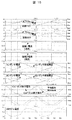
図10は2つの駆動回路が同時変化するタイミングである。図10では、2つの駆動回路のスイッチング素子4aとスイッチング素子4nをオフすると(図示:回路1オフ、回路2オフ)、還流ダイオード5aと還流ダイオード5nが順方向バイアスとなり(回路1電流(還流)、回路2電流(還流))、ソレノイド電流が還流して(図示:ソレノイド電流1、ソレノイド電流2)、コンデンサ6の両端電圧が時間経過とともに上昇する(図示:コンデンサ両端電圧)。そのため、インピーダンス素子7nに流れる電流も上昇して、スイッチング素子がオフからオンに遷移する点が最大電流となることが見てとれる(図示:インピーダンス素子電流)。インピーダンス素子7nには2つの駆動回路からのソレノイド電流が還流するため約2倍の電流となり、損失=R×Iの2乗より、損失は駆動回路が1つの場合の約4倍に増えてしまう。解析結果によれば、平均損失は約1160mWと大きいことが見てとれる(図示:インピーダンス素子損失)。
図11は、2つの駆動回路のPWM駆動の位相を半周期ずらした場合である。スイッチング素子4nをオフすると(図示:回路2オフ)、還流ダイオード5nが順方向バイアスとなり、ソレノイド電流が還流する(図示:ソレノイド2電流)。一方、スイッチング素子4aはオン状態にあり(図示:回路1オン)、還流ダイオード5nが逆方向バイアスとなり、還流はしない(図示:ソレノイド1電流)。このように、2つの駆動回路のうち一方が還流しないので(図示:回路1還流なし、回路2還流)、インピーダンス素子7nに流れる電流を低減することが出来る(図示:インピーダンス素子電流)。解析結果によれば、平均損失は約910mWまで抑えられることが見てとれる(図示:インピーダンス素子損失)。
さらには、図10で示すVBリプル電圧と(図示:リプル電圧)、図11に示すVBリプル電圧によれば(図示:リプル電圧)、PWMの位相をずらしたことにより、VBリプル電圧も大幅に低減出来るという効果が見てとれる。
図15と図16にて、図9の実施例に示す2つの駆動回路がある構成におけるインピーダンス素子7a、7nの損失を説明する。回路解析ツールによる解析波形と平均損失を示す。
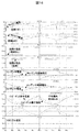
図15は2つの駆動回路が同時変化するタイミングである。図15は、2つの駆動回路のスイッチング素子4aをオフすると(図示:回路1オフ)、還流ダイオード5aが順方向バイアスとなり、ソレノイド電流が還流して(図示:ソレノイド1電流)、コンデンサ6aの両端電圧が時間経過とともに上昇する(図示:コンデンサ両端電圧)。そして、インピーダンス素子7aに流れる電流も上昇して(図示:インピーダンス素子電流)、スイッチング素子がオフからオンに遷移する点が最大電流となることが見てとれる。
また、スイッチング素子4nをオフすると(図示:回路2オフ)、還流ダイオード5nが順方向バイアスとなり、ソレノイド電流が還流して(図示:ソレノイド2電流)、コンデンサ6nの両端電圧が時間経過とともに上昇する(図示:コンデンサ両端電圧)。そして、インピーダンス素子7nに流れる電流も上昇して(図示:インピーダンス素子電流)、スイッチング素子がオフからオンに遷移する点が最大電流となることが見てとれる。解析ツールの結果によれば、平均損失は約330mWであることが見てとれる(図示:インピーダンス素子損失)。
また、スイッチング素子4nをオフすると(図示:回路2オフ)、還流ダイオード5nが順方向バイアスとなり、ソレノイド電流が還流して(図示:ソレノイド2電流)、コンデンサ6nの両端電圧が時間経過とともに上昇する(図示:コンデンサ両端電圧)。そして、インピーダンス素子7nに流れる電流も上昇して(図示:インピーダンス素子電流)、スイッチング素子がオフからオンに遷移する点が最大電流となることが見てとれる。解析ツールの結果によれば、平均損失は約330mWであることが見てとれる(図示:インピーダンス素子損失)。
図16は、2つの駆動回路のPWM駆動の位相を半周期ずらした場合である。スイッチング素子4nをオフすると(図示:回路2オフ)、還流ダイオード5nが順方向バイアスとなり、ソレノイド電流が還流する(図示:ソレノイド2電流)。一方、スイッチング素子4aはオン状態にあり(図示:回路1オン)、還流ダイオード5nが逆方向バイアスとなり、還流はしない(図示:ソレノイド1電流)。上記のように、両者共にスイッチング素子がオフからオンに遷移する点が最大電流となることが見てとれる(図示:インピーダンス素子電流)。 解析ツールの結果によれば、平均損失は320mWであることが見てとれる(図示:インピーダンス素子損失)。
このように、2つの駆動回路は各々にインピーダンス素子を配置することによって、両者の電流が合わさることがないため、損失が大きくなることがない。
このように、2つの駆動回路は各々にインピーダンス素子を配置することによって、両者の電流が合わさることがないため、損失が大きくなることがない。
以上の2つの形態から、インピーダンス素子を共用した場合における損失を改善するためには、電流のピーク時のタイミングをずらす手法が平均電流を下げることに繋がり、大きな損失削減の効果を得られることは明白である。
さらには、図15で示すVBリプル電圧(図示:リプル電圧)と図16に示すVBリプル電圧(図示:リプル電圧)によれば、PWMの位相をずらしたことにより、VBリプル電圧も大幅に低減出来るという効果が見てとれる。
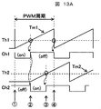
次に、実施例2に示す、2つの駆動回路がある構成における制御方法について説明する。図12と図13ともにマイコンのタイマモジュールを使用した場合のタイミング波形とブロック構成を示して実施例を説明する。
図12は、予め定めた位相差でタイミングをずらす制御方法である。図12Aはタイミング図であり、図12Bにブロック構成を示して動作の流れを説明する。
・(図12A1)定周期タイマ11aは、初期値はゼロである。基準クロックClkを入力して1つずつカウントアップを開始して、PWM周期毎にゼロクリアされるアップタイマである。Ch1=0は駆動回路1がオン状態、CH2=1は駆動回路2がオフ状態であることを示す。しきい値レジスタ12aは駆動回路1のPWMオン時間設定値、しきい値レジスタ12bは駆動回路2のPWMオン時間設定値、シフト値レジスタ14は、駆動回路2の位相差(タイミングずらし)の時間設定値であり、PWM周波数の半周期を設定値の例に説明する。
・(図12A1)定周期タイマ11aは、初期値はゼロである。基準クロックClkを入力して1つずつカウントアップを開始して、PWM周期毎にゼロクリアされるアップタイマである。Ch1=0は駆動回路1がオン状態、CH2=1は駆動回路2がオフ状態であることを示す。しきい値レジスタ12aは駆動回路1のPWMオン時間設定値、しきい値レジスタ12bは駆動回路2のPWMオン時間設定値、シフト値レジスタ14は、駆動回路2の位相差(タイミングずらし)の時間設定値であり、PWM周波数の半周期を設定値の例に説明する。
(図12A2)しきい値レジスタ12aの出力Th1は比較器13aに入力されて、定周期タイマ11aの出力Tm1より上回った時(A>Bが真)となり、Ch1が1となって駆動回路1がオフする。
(図12A3)定周期タイマ11aの値Tm1=シフト値レジスタ14の値Sftの時にCh2=0となって駆動回路2がオンする。
(図12A4)定周期タイマ11aの値Tm1>(シフト値レジスタ14の値Sft+しきい値レジスタ12bの値Th2)の時、比較器13bのCh2が1となって駆動回路2がオフする。
以上のように、予め定めた位相差でタイミングをずらす制御方法である。なお、位相差は、駆動回路が2つの場合として、半周期(PWM周期/2)で説明したが、駆動回路が増えた場合には、例えば、3回路ではPWM周期/3、4回路ではPWM周期/4が効果的であることは言うまでもない。
図13は、一方のタイマの終了イベントをトリガにして、もう一方のタイマを起動することでタイミングをずらす制御方法である。図13Aはタイミング図であり、図13Bに構成を示し、動作の流れを説明する。
(図13A1)定周期タイマ11aは、初期値はゼロである。基準クロックClkを入力して1つずつカウントアップを開始して、PWM周期毎にゼロクリアされるアップタイマである。Ch1=0は駆動回路1がオン状態、CH2=1は駆動回路2がオフ状態であることを表す。しきい値レジスタ12aは駆動回路1のPWMのオン時間設定値、しきい値レジスタ12bは駆動回路2のPWMのオン時間設定値である。
(図13A2)しきい値レジスタ12aの出力Th1は比較器13aに入力されて、定周期タイマ11aの出力Tm1より上回った時(A>Bが真)となり、Ch1が1となって駆動回路1がオフする。
同時に、Ch2が0となって駆動回路2をオンする(この時が、駆動回路1の電流最大で、駆動回路2の電流最小である。)。また、Chが1により、定周期タイマ11bのカウント許可ENがイネーブルとなり、基準クロックClkを入力して1つずつカウントアップを開始する。
(図12A3)定周期タイマ11bの値Tm2>しきい値レジスタ12bの値Th2の時、比較器13bのCh2が1となって駆動回路2がオフする。
以上のように、一方のタイマの終了イベントをトリガにして、もう一方のタイマを起動することでタイミングをずらす制御方法である。なお、本実施例では、2つの駆動回路のオン時間の総和が,PWM周期を超えてはならないことは(駆動回路が増えた場合、例えば、3回路、4回路でも同様である)、言うまでもない。
1…電磁コイルの駆動制御装置、2…直流電源、3、3a、3n…電磁コイル(ソレノイド)、4、4a、4n…スイッチング素子、5、5a、5n…還流ダイオード、6、6a、6n…コンデンサ、7、7a、7n…インピーダンス素子、L1…正極ライン、L2、L3、L4…接続ライン、L5…負極ライン、L2a、L2n、L3a、L3n、L4a、L4n…接続ライン。
11a、11b…定周期タイマ、12a、12b…しきい値レジスタ、
13a、13b…比較器、14…シフト値レジスタ、15…加算器
11a、11b…定周期タイマ、12a、12b…しきい値レジスタ、
13a、13b…比較器、14…シフト値レジスタ、15…加算器
Claims (6)
- 直流電源の正極側に一端が接続された第一の電磁コイルと、
前記第一の電磁コイルに流れる電流をオン/オフするため前記第一の電磁コイルの他端と接続された第一のスイッチング素子と、
前記第一のスイッチング素子がオフしたときに前記第一の電磁コイルに蓄えられた電気的なエネルギーをフリーホイール電流として還流させる第一の還流ダイオードを備え、
前記直流電源の正極ラインと負極ラインとを接続する接続ラインにコンデンサとインピーダンス素子を直列に配置し、前記コンデンサと前記インピーダンス素子の間の前記接続ラインと前記第一の電磁コイルの他端とを前記第一の還流ダイオードを介して接続し、
前記直流電源の正極側に一端が接続された第二の電磁コイルと、
前記第二の電磁コイルに流れる電流をオン/オフするため前記第二の電磁コイルの他端と接続された第二のスイッチング素子と、
前記第二のスイッチング素子がオフしたときに前記第二の電磁コイルに蓄えられた電気的なエネルギーをフリーホイール電流として還流させる第二の還流ダイオードを備え、
前記直流電源の正極ラインと負極ラインとを接続する接続ラインに前記コンデンサと前記インピーダンス素子を直列に配置し、前記コンデンサと前記インピーダンス素子の間の前記接続ラインと前記第二の電磁コイルの他端とを前記第二の還流ダイオードを介して接続し、
前記第一のスイッチング素子と前記第二のスイッチング素子の動作は、オンとオン、あるいはオフとオフの動作が同時に重ならないようにタイミングをずらして駆動されることを特徴とする電磁コイルの駆動制御装置。 - 直流電源の正極側に一端が接続された第一の電磁コイルと、
前記第一の電磁コイルに流れる電流をオン/オフするため前記第一の電磁コイルの他端と接続された第一のスイッチング素子と、
前記第一のスイッチング素子がオフしたときに前記第一の電磁コイルに蓄えられた電気的なエネルギーをフリーホイール電流として還流させる第一の還流ダイオードを備え、
前記直流電源の正極ラインと負極ラインとを接続する接続ラインに第一のコンデンサと第一のインピーダンス素子を直列に配置し、前記第一のコンデンサと前記第一のインピーダンス素子の間の前記接続ラインと前記第一の電磁コイルの他端とを前記第一の還流ダイオードを介して接続し、
前記直流電源の正極側に一端が接続された第二の電磁コイルと、
前記第二の電磁コイルに流れる電流をオン/オフするため前記第二の電磁コイルの他端と接続された第二のスイッチング素子と、
前記第二のスイッチング素子がオフしたときに前記第二の電磁コイルに蓄えられた電気的なエネルギーをフリーホイール電流として還流させる第二の還流ダイオードを備え、
前記直流電源の正極ラインと負極ラインとを接続する接続ラインに第二のコンデンサと第二のインピーダンス素子を直列に配置し、前記第二のコンデンサと前記第二のインピーダンス素子の間の前記接続ラインと前記第二の電磁コイルの他端とを前記第二の還流ダイオードを介して接続し、
前記第一のスイッチング素子と前記第二のスイッチング素子の動作は、オンとオン、あるいはオフとオフの動作が同時に重ならないようにタイミングをずらして駆動されることを特徴とする電磁コイルの駆動制御装置。 - 請求項1に記載の電磁コイルの駆動制御装置において、
前記第一のスイッチング素子と前記第二のスイッチング素子のオン/オフ動作タイミングをずらしてなる制御は、
前記第一のスイッチング素子と前記第二のスイッチング素子の一方がオンした後に、他方があらかじめ定めた位相差の後にオンするようにタイミングをずらす制御方法からなることを特徴とする電磁コイルの駆動制御装置。 - 請求項2に記載の電磁コイルの駆動制御装置において、
前記第一のスイッチング素子と前記第二のスイッチング素子のオン/オフ動作タイミングをずらしてなる制御は、
前記第一のスイッチング素子と前記第二のスイッチング素子の一方がオンした後に、他方があらかじめ定めた位相差の後にオンするようにタイミングをずらす制御方法からなることを特徴とする電磁コイルの駆動制御装置。 - 請求項1に記載の電磁コイルの駆動制御装置において、
前記第一のスイッチング素子と前記第二のスイッチング素子のオン/オフ動作タイミングをずらしてなる制御は、
前記第一のスイッチング素子と前記第二のスイッチング素子の一方のオフした後に、他方がオンするようにタイミングをずらす制御方法からなることを特徴とする電磁コイルの駆動制御装置。 - 請求項2に記載の電磁コイルの駆動制御装置において、
前記第一のスイッチング素子と前記第二のスイッチング素子のオン/オフ動作タイミングをずらしてなる制御は、
前記第一のスイッチング素子と前記第二のスイッチング素子の一方のオフした後に、他方がオンするようにタイミングをずらす制御方法からなることを特徴とする電磁コイルの駆動制御装置。
Applications Claiming Priority (2)
| Application Number | Priority Date | Filing Date | Title |
|---|---|---|---|
| JP2014002082A JP6240511B2 (ja) | 2014-01-09 | 2014-01-09 | 電子制御ユニット |
| JP2014-002082 | 2014-01-09 |
Publications (1)
| Publication Number | Publication Date |
|---|---|
| WO2015104920A1 true WO2015104920A1 (ja) | 2015-07-16 |
Family
ID=53523758
Family Applications (1)
| Application Number | Title | Priority Date | Filing Date |
|---|---|---|---|
| PCT/JP2014/081925 Ceased WO2015104920A1 (ja) | 2014-01-09 | 2014-12-03 | 電子制御ユニット |
Country Status (2)
| Country | Link |
|---|---|
| JP (1) | JP6240511B2 (ja) |
| WO (1) | WO2015104920A1 (ja) |
Cited By (1)
| Publication number | Priority date | Publication date | Assignee | Title |
|---|---|---|---|---|
| EP3190325A1 (en) * | 2016-01-08 | 2017-07-12 | Goodrich Actuation Systems Limited | Heating of solenoids |
Citations (3)
| Publication number | Priority date | Publication date | Assignee | Title |
|---|---|---|---|---|
| JPH1012436A (ja) * | 1996-06-18 | 1998-01-16 | Unisia Jecs Corp | 電磁アクチュエータ駆動制御回路 |
| JP2003049687A (ja) * | 2001-08-02 | 2003-02-21 | Mikuni Corp | ソレノイド駆動装置 |
| JP2013108476A (ja) * | 2011-11-24 | 2013-06-06 | Denso Corp | 燃料噴射制御装置用電磁弁駆動装置 |
Family Cites Families (2)
| Publication number | Priority date | Publication date | Assignee | Title |
|---|---|---|---|---|
| JP3422002B2 (ja) * | 1994-11-11 | 2003-06-30 | 株式会社小松製作所 | Dc−dcコンバータ回路およびこのdc−dcコンバータ回路を用いた誘導負荷駆動装置 |
| JP3058869B1 (ja) * | 1999-01-29 | 2000-07-04 | 株式会社タクミナ | ソレノイド駆動回路 |
-
2014
- 2014-01-09 JP JP2014002082A patent/JP6240511B2/ja not_active Expired - Fee Related
- 2014-12-03 WO PCT/JP2014/081925 patent/WO2015104920A1/ja not_active Ceased
Patent Citations (3)
| Publication number | Priority date | Publication date | Assignee | Title |
|---|---|---|---|---|
| JPH1012436A (ja) * | 1996-06-18 | 1998-01-16 | Unisia Jecs Corp | 電磁アクチュエータ駆動制御回路 |
| JP2003049687A (ja) * | 2001-08-02 | 2003-02-21 | Mikuni Corp | ソレノイド駆動装置 |
| JP2013108476A (ja) * | 2011-11-24 | 2013-06-06 | Denso Corp | 燃料噴射制御装置用電磁弁駆動装置 |
Cited By (3)
| Publication number | Priority date | Publication date | Assignee | Title |
|---|---|---|---|---|
| EP3190325A1 (en) * | 2016-01-08 | 2017-07-12 | Goodrich Actuation Systems Limited | Heating of solenoids |
| US10663078B2 (en) | 2016-01-08 | 2020-05-26 | Goodrich Actuation Systems Limited | Heating of solenoids |
| US11493143B2 (en) | 2016-01-08 | 2022-11-08 | Goodrich Actuation Systems Limited | Heating of solenoids |
Also Published As
| Publication number | Publication date |
|---|---|
| JP6240511B2 (ja) | 2017-11-29 |
| JP2015130454A (ja) | 2015-07-16 |
Similar Documents
| Publication | Publication Date | Title |
|---|---|---|
| JP3422002B2 (ja) | Dc−dcコンバータ回路およびこのdc−dcコンバータ回路を用いた誘導負荷駆動装置 | |
| US9391532B2 (en) | System and method for a switched-mode power converter | |
| EP2323245B1 (en) | Voltage conversion apparatus and electrical load drive apparatus | |
| EP1653066B1 (en) | Device for controlling fuel electro-injectors and electrovalves in an internal-combustion engine, and method of operating the same. | |
| WO2016136187A1 (ja) | 双方向コンバータ、コントローラ、および半導体装置 | |
| JP6066531B2 (ja) | 電磁コイルの駆動制御装置 | |
| CN102575603B (zh) | 用于多个感应负载的控制电路和用于控制感应负载的方法 | |
| JP6240511B2 (ja) | 電子制御ユニット | |
| EP2665186B1 (en) | Electronic control apparatus for controlling driving of load by mos fets | |
| JP2021064981A (ja) | Dcdcコンバータ | |
| JP4621767B2 (ja) | 電圧変換装置及び電気負荷駆動装置 | |
| EP3127398A1 (de) | Gargerätevorrichtung | |
| CN116633137A (zh) | 一种基于耦合电感具备连续输入输出电流的dc-dc变换器 | |
| US9281757B2 (en) | Voltage conversion device and electrical load driving device | |
| JP5841098B2 (ja) | ゼロカレントスイッチング回路及びフルブリッジ回路 | |
| CN109036962B (zh) | 一种继电器线圈节能的驱动电路 | |
| CN121429518A (zh) | 一种迟滞电流控制喷油电路及其控制方法 | |
| JP2024055468A (ja) | 電源装置 | |
| JPH07337085A (ja) | 電動モータの制御装置 | |
| CN114097169A (zh) | 用于供电网络的多相变压器和用于降低该供电网络的中间电路电压的方法 |
Legal Events
| Date | Code | Title | Description |
|---|---|---|---|
| 121 | Ep: the epo has been informed by wipo that ep was designated in this application |
Ref document number: 14877670 Country of ref document: EP Kind code of ref document: A1 |
|
| NENP | Non-entry into the national phase |
Ref country code: DE |
|
| 122 | Ep: pct application non-entry in european phase |
Ref document number: 14877670 Country of ref document: EP Kind code of ref document: A1 |