WO2015093038A1 - Semiconductor device - Google Patents
Semiconductor device Download PDFInfo
- Publication number
- WO2015093038A1 WO2015093038A1 PCT/JP2014/006244 JP2014006244W WO2015093038A1 WO 2015093038 A1 WO2015093038 A1 WO 2015093038A1 JP 2014006244 W JP2014006244 W JP 2014006244W WO 2015093038 A1 WO2015093038 A1 WO 2015093038A1
- Authority
- WO
- WIPO (PCT)
- Prior art keywords
- region
- igbt
- layer
- conductivity type
- diode
- Prior art date
Links
- 239000004065 semiconductor Substances 0.000 title claims abstract description 54
- 238000002347 injection Methods 0.000 claims abstract description 81
- 239000007924 injection Substances 0.000 claims abstract description 81
- 239000012535 impurity Substances 0.000 claims abstract description 74
- 230000009467 reduction Effects 0.000 claims abstract description 19
- 239000010410 layer Substances 0.000 claims description 135
- 239000000758 substrate Substances 0.000 claims description 26
- 239000002344 surface layer Substances 0.000 claims description 13
- 210000000746 body region Anatomy 0.000 claims 7
- 238000009792 diffusion process Methods 0.000 description 14
- 230000015572 biosynthetic process Effects 0.000 description 12
- 238000005468 ion implantation Methods 0.000 description 12
- 238000010586 diagram Methods 0.000 description 11
- 239000000969 carrier Substances 0.000 description 8
- 238000004519 manufacturing process Methods 0.000 description 6
- 239000011295 pitch Substances 0.000 description 6
- 238000000137 annealing Methods 0.000 description 5
- 238000009826 distribution Methods 0.000 description 5
- OAICVXFJPJFONN-UHFFFAOYSA-N Phosphorus Chemical compound [P] OAICVXFJPJFONN-UHFFFAOYSA-N 0.000 description 4
- 230000008859 change Effects 0.000 description 4
- 230000000694 effects Effects 0.000 description 4
- 238000000034 method Methods 0.000 description 4
- 229910052698 phosphorus Inorganic materials 0.000 description 4
- 239000011574 phosphorus Substances 0.000 description 4
- ZOXJGFHDIHLPTG-UHFFFAOYSA-N Boron Chemical compound [B] ZOXJGFHDIHLPTG-UHFFFAOYSA-N 0.000 description 2
- 229910052796 boron Inorganic materials 0.000 description 2
- 230000007547 defect Effects 0.000 description 2
- 239000007772 electrode material Substances 0.000 description 2
- 238000002474 experimental method Methods 0.000 description 2
- 239000011229 interlayer Substances 0.000 description 2
- 150000002500 ions Chemical class 0.000 description 2
- 229910021420 polycrystalline silicon Inorganic materials 0.000 description 2
- 230000008569 process Effects 0.000 description 2
- 230000007423 decrease Effects 0.000 description 1
- 230000006866 deterioration Effects 0.000 description 1
- 238000005530 etching Methods 0.000 description 1
- 230000005669 field effect Effects 0.000 description 1
- 238000010438 heat treatment Methods 0.000 description 1
- 238000009413 insulation Methods 0.000 description 1
- 238000005224 laser annealing Methods 0.000 description 1
- 230000003647 oxidation Effects 0.000 description 1
- 238000007254 oxidation reaction Methods 0.000 description 1
- 238000002161 passivation Methods 0.000 description 1
- 238000000059 patterning Methods 0.000 description 1
- 230000002093 peripheral effect Effects 0.000 description 1
- 229920005591 polysilicon Polymers 0.000 description 1
- 229920006395 saturated elastomer Polymers 0.000 description 1
- 238000004088 simulation Methods 0.000 description 1
Images


Classifications
-
- H—ELECTRICITY
- H01—ELECTRIC ELEMENTS
- H01L—SEMICONDUCTOR DEVICES NOT COVERED BY CLASS H10
- H01L27/00—Devices consisting of a plurality of semiconductor or other solid-state components formed in or on a common substrate
- H01L27/02—Devices consisting of a plurality of semiconductor or other solid-state components formed in or on a common substrate including semiconductor components specially adapted for rectifying, oscillating, amplifying or switching and having at least one potential-jump barrier or surface barrier; including integrated passive circuit elements with at least one potential-jump barrier or surface barrier
- H01L27/04—Devices consisting of a plurality of semiconductor or other solid-state components formed in or on a common substrate including semiconductor components specially adapted for rectifying, oscillating, amplifying or switching and having at least one potential-jump barrier or surface barrier; including integrated passive circuit elements with at least one potential-jump barrier or surface barrier the substrate being a semiconductor body
- H01L27/06—Devices consisting of a plurality of semiconductor or other solid-state components formed in or on a common substrate including semiconductor components specially adapted for rectifying, oscillating, amplifying or switching and having at least one potential-jump barrier or surface barrier; including integrated passive circuit elements with at least one potential-jump barrier or surface barrier the substrate being a semiconductor body including a plurality of individual components in a non-repetitive configuration
- H01L27/07—Devices consisting of a plurality of semiconductor or other solid-state components formed in or on a common substrate including semiconductor components specially adapted for rectifying, oscillating, amplifying or switching and having at least one potential-jump barrier or surface barrier; including integrated passive circuit elements with at least one potential-jump barrier or surface barrier the substrate being a semiconductor body including a plurality of individual components in a non-repetitive configuration the components having an active region in common
- H01L27/0705—Devices consisting of a plurality of semiconductor or other solid-state components formed in or on a common substrate including semiconductor components specially adapted for rectifying, oscillating, amplifying or switching and having at least one potential-jump barrier or surface barrier; including integrated passive circuit elements with at least one potential-jump barrier or surface barrier the substrate being a semiconductor body including a plurality of individual components in a non-repetitive configuration the components having an active region in common comprising components of the field effect type
- H01L27/0711—Devices consisting of a plurality of semiconductor or other solid-state components formed in or on a common substrate including semiconductor components specially adapted for rectifying, oscillating, amplifying or switching and having at least one potential-jump barrier or surface barrier; including integrated passive circuit elements with at least one potential-jump barrier or surface barrier the substrate being a semiconductor body including a plurality of individual components in a non-repetitive configuration the components having an active region in common comprising components of the field effect type in combination with bipolar transistors and diodes, or capacitors, or resistors
- H01L27/0716—Devices consisting of a plurality of semiconductor or other solid-state components formed in or on a common substrate including semiconductor components specially adapted for rectifying, oscillating, amplifying or switching and having at least one potential-jump barrier or surface barrier; including integrated passive circuit elements with at least one potential-jump barrier or surface barrier the substrate being a semiconductor body including a plurality of individual components in a non-repetitive configuration the components having an active region in common comprising components of the field effect type in combination with bipolar transistors and diodes, or capacitors, or resistors in combination with vertical bipolar transistors and diodes, or capacitors, or resistors
-
- H—ELECTRICITY
- H01—ELECTRIC ELEMENTS
- H01L—SEMICONDUCTOR DEVICES NOT COVERED BY CLASS H10
- H01L27/00—Devices consisting of a plurality of semiconductor or other solid-state components formed in or on a common substrate
- H01L27/02—Devices consisting of a plurality of semiconductor or other solid-state components formed in or on a common substrate including semiconductor components specially adapted for rectifying, oscillating, amplifying or switching and having at least one potential-jump barrier or surface barrier; including integrated passive circuit elements with at least one potential-jump barrier or surface barrier
- H01L27/04—Devices consisting of a plurality of semiconductor or other solid-state components formed in or on a common substrate including semiconductor components specially adapted for rectifying, oscillating, amplifying or switching and having at least one potential-jump barrier or surface barrier; including integrated passive circuit elements with at least one potential-jump barrier or surface barrier the substrate being a semiconductor body
- H01L27/06—Devices consisting of a plurality of semiconductor or other solid-state components formed in or on a common substrate including semiconductor components specially adapted for rectifying, oscillating, amplifying or switching and having at least one potential-jump barrier or surface barrier; including integrated passive circuit elements with at least one potential-jump barrier or surface barrier the substrate being a semiconductor body including a plurality of individual components in a non-repetitive configuration
- H01L27/07—Devices consisting of a plurality of semiconductor or other solid-state components formed in or on a common substrate including semiconductor components specially adapted for rectifying, oscillating, amplifying or switching and having at least one potential-jump barrier or surface barrier; including integrated passive circuit elements with at least one potential-jump barrier or surface barrier the substrate being a semiconductor body including a plurality of individual components in a non-repetitive configuration the components having an active region in common
- H01L27/0705—Devices consisting of a plurality of semiconductor or other solid-state components formed in or on a common substrate including semiconductor components specially adapted for rectifying, oscillating, amplifying or switching and having at least one potential-jump barrier or surface barrier; including integrated passive circuit elements with at least one potential-jump barrier or surface barrier the substrate being a semiconductor body including a plurality of individual components in a non-repetitive configuration the components having an active region in common comprising components of the field effect type
- H01L27/0727—Devices consisting of a plurality of semiconductor or other solid-state components formed in or on a common substrate including semiconductor components specially adapted for rectifying, oscillating, amplifying or switching and having at least one potential-jump barrier or surface barrier; including integrated passive circuit elements with at least one potential-jump barrier or surface barrier the substrate being a semiconductor body including a plurality of individual components in a non-repetitive configuration the components having an active region in common comprising components of the field effect type in combination with diodes, or capacitors or resistors
-
- H—ELECTRICITY
- H01—ELECTRIC ELEMENTS
- H01L—SEMICONDUCTOR DEVICES NOT COVERED BY CLASS H10
- H01L29/00—Semiconductor devices adapted for rectifying, amplifying, oscillating or switching, or capacitors or resistors with at least one potential-jump barrier or surface barrier, e.g. PN junction depletion layer or carrier concentration layer; Details of semiconductor bodies or of electrodes thereof ; Multistep manufacturing processes therefor
- H01L29/02—Semiconductor bodies ; Multistep manufacturing processes therefor
- H01L29/06—Semiconductor bodies ; Multistep manufacturing processes therefor characterised by their shape; characterised by the shapes, relative sizes, or dispositions of the semiconductor regions ; characterised by the concentration or distribution of impurities within semiconductor regions
- H01L29/08—Semiconductor bodies ; Multistep manufacturing processes therefor characterised by their shape; characterised by the shapes, relative sizes, or dispositions of the semiconductor regions ; characterised by the concentration or distribution of impurities within semiconductor regions with semiconductor regions connected to an electrode carrying current to be rectified, amplified or switched and such electrode being part of a semiconductor device which comprises three or more electrodes
- H01L29/083—Anode or cathode regions of thyristors or gated bipolar-mode devices
- H01L29/0834—Anode regions of thyristors or gated bipolar-mode devices, e.g. supplementary regions surrounding anode regions
-
- H—ELECTRICITY
- H01—ELECTRIC ELEMENTS
- H01L—SEMICONDUCTOR DEVICES NOT COVERED BY CLASS H10
- H01L29/00—Semiconductor devices adapted for rectifying, amplifying, oscillating or switching, or capacitors or resistors with at least one potential-jump barrier or surface barrier, e.g. PN junction depletion layer or carrier concentration layer; Details of semiconductor bodies or of electrodes thereof ; Multistep manufacturing processes therefor
- H01L29/66—Types of semiconductor device ; Multistep manufacturing processes therefor
- H01L29/68—Types of semiconductor device ; Multistep manufacturing processes therefor controllable by only the electric current supplied, or only the electric potential applied, to an electrode which does not carry the current to be rectified, amplified or switched
- H01L29/70—Bipolar devices
- H01L29/72—Transistor-type devices, i.e. able to continuously respond to applied control signals
- H01L29/739—Transistor-type devices, i.e. able to continuously respond to applied control signals controlled by field-effect, e.g. bipolar static induction transistors [BSIT]
- H01L29/7393—Insulated gate bipolar mode transistors, i.e. IGBT; IGT; COMFET
- H01L29/7395—Vertical transistors, e.g. vertical IGBT
- H01L29/7396—Vertical transistors, e.g. vertical IGBT with a non planar surface, e.g. with a non planar gate or with a trench or recess or pillar in the surface of the emitter, base or collector region for improving current density or short circuiting the emitter and base regions
- H01L29/7397—Vertical transistors, e.g. vertical IGBT with a non planar surface, e.g. with a non planar gate or with a trench or recess or pillar in the surface of the emitter, base or collector region for improving current density or short circuiting the emitter and base regions and a gate structure lying on a slanted or vertical surface or formed in a groove, e.g. trench gate IGBT
-
- H—ELECTRICITY
- H01—ELECTRIC ELEMENTS
- H01L—SEMICONDUCTOR DEVICES NOT COVERED BY CLASS H10
- H01L29/00—Semiconductor devices adapted for rectifying, amplifying, oscillating or switching, or capacitors or resistors with at least one potential-jump barrier or surface barrier, e.g. PN junction depletion layer or carrier concentration layer; Details of semiconductor bodies or of electrodes thereof ; Multistep manufacturing processes therefor
- H01L29/66—Types of semiconductor device ; Multistep manufacturing processes therefor
- H01L29/68—Types of semiconductor device ; Multistep manufacturing processes therefor controllable by only the electric current supplied, or only the electric potential applied, to an electrode which does not carry the current to be rectified, amplified or switched
- H01L29/76—Unipolar devices, e.g. field effect transistors
- H01L29/772—Field effect transistors
- H01L29/78—Field effect transistors with field effect produced by an insulated gate
-
- H—ELECTRICITY
- H01—ELECTRIC ELEMENTS
- H01L—SEMICONDUCTOR DEVICES NOT COVERED BY CLASS H10
- H01L29/00—Semiconductor devices adapted for rectifying, amplifying, oscillating or switching, or capacitors or resistors with at least one potential-jump barrier or surface barrier, e.g. PN junction depletion layer or carrier concentration layer; Details of semiconductor bodies or of electrodes thereof ; Multistep manufacturing processes therefor
- H01L29/02—Semiconductor bodies ; Multistep manufacturing processes therefor
- H01L29/06—Semiconductor bodies ; Multistep manufacturing processes therefor characterised by their shape; characterised by the shapes, relative sizes, or dispositions of the semiconductor regions ; characterised by the concentration or distribution of impurities within semiconductor regions
- H01L29/10—Semiconductor bodies ; Multistep manufacturing processes therefor characterised by their shape; characterised by the shapes, relative sizes, or dispositions of the semiconductor regions ; characterised by the concentration or distribution of impurities within semiconductor regions with semiconductor regions connected to an electrode not carrying current to be rectified, amplified or switched and such electrode being part of a semiconductor device which comprises three or more electrodes
- H01L29/107—Substrate region of field-effect devices
- H01L29/1075—Substrate region of field-effect devices of field-effect transistors
- H01L29/1079—Substrate region of field-effect devices of field-effect transistors with insulated gate
- H01L29/1087—Substrate region of field-effect devices of field-effect transistors with insulated gate characterised by the contact structure of the substrate region, e.g. for controlling or preventing bipolar effect
-
- H—ELECTRICITY
- H01—ELECTRIC ELEMENTS
- H01L—SEMICONDUCTOR DEVICES NOT COVERED BY CLASS H10
- H01L29/00—Semiconductor devices adapted for rectifying, amplifying, oscillating or switching, or capacitors or resistors with at least one potential-jump barrier or surface barrier, e.g. PN junction depletion layer or carrier concentration layer; Details of semiconductor bodies or of electrodes thereof ; Multistep manufacturing processes therefor
- H01L29/02—Semiconductor bodies ; Multistep manufacturing processes therefor
- H01L29/06—Semiconductor bodies ; Multistep manufacturing processes therefor characterised by their shape; characterised by the shapes, relative sizes, or dispositions of the semiconductor regions ; characterised by the concentration or distribution of impurities within semiconductor regions
- H01L29/10—Semiconductor bodies ; Multistep manufacturing processes therefor characterised by their shape; characterised by the shapes, relative sizes, or dispositions of the semiconductor regions ; characterised by the concentration or distribution of impurities within semiconductor regions with semiconductor regions connected to an electrode not carrying current to be rectified, amplified or switched and such electrode being part of a semiconductor device which comprises three or more electrodes
- H01L29/1095—Body region, i.e. base region, of DMOS transistors or IGBTs
-
- H—ELECTRICITY
- H01—ELECTRIC ELEMENTS
- H01L—SEMICONDUCTOR DEVICES NOT COVERED BY CLASS H10
- H01L29/00—Semiconductor devices adapted for rectifying, amplifying, oscillating or switching, or capacitors or resistors with at least one potential-jump barrier or surface barrier, e.g. PN junction depletion layer or carrier concentration layer; Details of semiconductor bodies or of electrodes thereof ; Multistep manufacturing processes therefor
- H01L29/02—Semiconductor bodies ; Multistep manufacturing processes therefor
- H01L29/30—Semiconductor bodies ; Multistep manufacturing processes therefor characterised by physical imperfections; having polished or roughened surface
- H01L29/32—Semiconductor bodies ; Multistep manufacturing processes therefor characterised by physical imperfections; having polished or roughened surface the imperfections being within the semiconductor body
-
- H—ELECTRICITY
- H01—ELECTRIC ELEMENTS
- H01L—SEMICONDUCTOR DEVICES NOT COVERED BY CLASS H10
- H01L29/00—Semiconductor devices adapted for rectifying, amplifying, oscillating or switching, or capacitors or resistors with at least one potential-jump barrier or surface barrier, e.g. PN junction depletion layer or carrier concentration layer; Details of semiconductor bodies or of electrodes thereof ; Multistep manufacturing processes therefor
- H01L29/02—Semiconductor bodies ; Multistep manufacturing processes therefor
- H01L29/36—Semiconductor bodies ; Multistep manufacturing processes therefor characterised by the concentration or distribution of impurities in the bulk material
-
- H—ELECTRICITY
- H01—ELECTRIC ELEMENTS
- H01L—SEMICONDUCTOR DEVICES NOT COVERED BY CLASS H10
- H01L29/00—Semiconductor devices adapted for rectifying, amplifying, oscillating or switching, or capacitors or resistors with at least one potential-jump barrier or surface barrier, e.g. PN junction depletion layer or carrier concentration layer; Details of semiconductor bodies or of electrodes thereof ; Multistep manufacturing processes therefor
- H01L29/66—Types of semiconductor device ; Multistep manufacturing processes therefor
- H01L29/86—Types of semiconductor device ; Multistep manufacturing processes therefor controllable only by variation of the electric current supplied, or only the electric potential applied, to one or more of the electrodes carrying the current to be rectified, amplified, oscillated or switched
- H01L29/861—Diodes
- H01L29/8613—Mesa PN junction diodes
Definitions
- the present disclosure relates to a semiconductor device in which both an insulated gate field effect transistor (hereinafter referred to as IGBT) and a free wheel diode (hereinafter simply referred to as a diode) are formed on one substrate.
- IGBT insulated gate field effect transistor
- diode free wheel diode
- Patent Document 1 proposes a semiconductor device in which an IGBT and a diode provided in a circuit such as an inverter are provided in parallel.
- lifetime control is performed by the following method.
- a semiconductor substrate in which an IGBT and a diode are both formed on one substrate is prepared. Then, ion implantation is performed from the substrate surface side to the IGBT and diode formation positions, and ion implantation is performed from the substrate rear surface side to the diode formation positions, followed by annealing. Thereby, a defect is formed in the portion where ion implantation has been performed, and lifetime control can be performed.
- lifetime control is generally performed by performing ion implantation from the back side of the substrate to the entire area where the IGBT and the diode are formed.
- the lifetime control of the IGBT and the diode is performed simultaneously, and the lifetime control of the IGBT and the diode cannot be individually optimized and performed.
- the present disclosure provides the characteristics of the IGBT and the diode separately without damaging the gate insulating film by ion implantation and minimizing lifetime control, preferably without performing lifetime control.
- An object is to provide a semiconductor device that can be optimized.
- a semiconductor device includes an IGBT portion in which a vertical IGBT is formed, and a diode portion provided along the IGBT portion and in which a diode is formed, a drift layer, a collector
- the region includes a region, a cathode region, a second conductivity type region, a trench, an emitter region, a hole injection reducing layer, a gate insulating film, a gate electrode, an upper electrode, and a lower electrode.
- the drift layer has the first conductivity type.
- the collector region has a second conductivity type, and is formed on the back surface side of the drift layer in the IGBT portion.
- the cathode region has a first conductivity type, and is formed on the back side of the drift layer in the diode portion.
- the second conductivity type region is formed in both the IGBT part and the diode part in the surface layer part on the surface side of the drift layer.
- a plurality of the trenches are arranged in the IGBT portion, are formed deeper than the second conductivity type region, and divide the second conductivity type region into a plurality of parts, so that at least a part of the second conductivity type region is formed. Configure the channel region.
- the emitter region has a first conductivity type, and is formed along a side surface of the trench in a surface layer portion of the channel region in the IGBT portion.
- the hole injection reducing layer has a first conductivity type, is formed in an upper layer portion of the drift layer in the diode portion, and is deeper and less impurity than an anode region constituted by the second conductivity type region in the diode portion. The impurity concentration is higher than that of the drift layer.
- the gate insulating film is formed on the surface of the trench.
- the gate electrode is formed on the surface of the gate insulating film.
- the upper electrode is electrically connected to the second conductivity type region in the IGBT portion and electrically connected to the anode region.
- the lower electrode is electrically connected to the collector region in the IGBT portion and electrically connected to the cathode region in the diode portion.
- the semiconductor device includes the hole injection reducing layer in the diode portion. For this reason, it becomes possible to reduce the holes injected through the diode part during the operation of the IGBT. As a result, AC loss during switching can be reduced. Further, AC loss and DC loss that is in a trade-off relationship with AC loss can be adjusted according to the impurity concentration of the hole injection reducing layer. Therefore, by providing the hole injection reducing layer in the diode portion, AC loss and DC loss can be set optimally, so that the characteristics of the IGBT and the diode can be optimized separately.
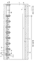
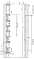
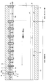
- FIG. 1 is a cross-sectional view of a semiconductor device including an IGBT and a diode according to the first embodiment of the present disclosure.
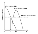
- FIG. 2 is a diagram showing the impurity concentration distribution of the p-type region and the hole injection reduction layer.
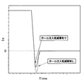
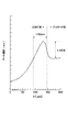
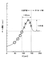
- FIG. 3 is a diagram showing a result of measuring a change in the collector current Ic when the IGBT is turned off.
- FIG. 4 is a diagram showing each concentration distribution when the impurity concentration peak of the hole injection reducing layer is changed.
- FIG. 1 is a cross-sectional view of a semiconductor device including an IGBT and a diode according to the first embodiment of the present disclosure.
- FIG. 2 is a diagram showing the impurity concentration distribution of the p-type region and the hole injection reduction layer.
- FIG. 3 is a diagram showing a result of measuring a change in the collector current Ic when the IGBT is turned off.
- FIG. 4 is a diagram showing each concentration distribution when the impurity concentration peak of the
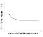
- FIG. 5 is a diagram showing the results of examining the AC loss and DC loss when the impurity concentration peak of the hole injection reducing layer is changed.
- FIG. 6 is a diagram showing the results of examining the relationship between AC loss and DC loss for each of the structure of the first embodiment provided with the hole injection reducing layer and the conventional structure not provided.
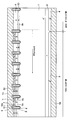
- FIG. 7 is a cross-sectional view of a semiconductor device including an IGBT and a diode according to the second embodiment of the present disclosure.
- FIG. 8 is a cross-sectional view of a semiconductor device including an IGBT and a diode according to the third embodiment of the present disclosure.
- FIG. 9 is a diagram showing a hole distribution when a hole injection reducing layer is not formed in the IGBT portion.
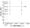
- FIG. 10 is a diagram showing the results of examining AC loss and DC loss when the amount of protrusion of the hole injection reducing layer is changed.
- FIG. 11 is a diagram showing the result of examining the total loss in the diode portion when the amount of protrusion of the hole injection reducing layer is changed.
- FIG. 12 is a cross-sectional view of a semiconductor device including an IGBT and a diode according to the fourth embodiment of the present disclosure.
- FIG. 13 is a cross-sectional view of a semiconductor device including an IGBT and a diode according to the fifth embodiment of the present disclosure.
- FIG. 14 is a diagram showing a comparison result of the hole distribution and the hole density of the IGBT part and the diode part when the hole injection reducing layer is not formed in the IGBT part.
- FIG. 15 is a diagram showing the relationship of the ratio L1 / T1 between the protrusion amount L1 and the plate thickness T1 with respect to the change in the impurity concentration in the body p-type region.
- FIG. 16 is a diagram showing the results of examining the relationship between the plate thickness T1 and the hole diffusion length by changing the impurity concentration in the body p-type region.
- the semiconductor device according to the present embodiment is configured by providing a vertical IGBT and a diode that allow current to flow in the substrate thickness direction on one substrate.
- the semiconductor device according to the present embodiment is configured as follows.
- the semiconductor device includes an IGBT unit 100 provided with an IGBT, and a diode unit 200 provided along the IGBT unit 100 and formed with a diode. ing.
- the IGBT unit 100 and the diode unit 200 are formed, for example, in a cell region in the center of the chip, and an outer peripheral pressure-resistant unit (not shown) is arranged on the outer periphery of the cell region, that is, on the outer edge of the chip.
- the semiconductor device concerning this is comprised.
- the IGBT and the diode are formed using a semiconductor substrate constituting the n ⁇ type drift layer 1.
- a field stop (hereinafter referred to as FS) layer 2 composed of an n-type layer is formed on the surface layer portion of n ⁇ -type drift layer 1 on the back surface side of n ⁇ -type drift layer 1.
- the FS layer 2 is formed from the back surface of the n ⁇ -type drift layer 1 to a relatively shallow position of a predetermined depth, and is configured by implanting an n-type impurity such as phosphorus (P).
- P n-type impurity
- the impurity concentration and diffusion depth of the FS layer 2 are set according to the required characteristics of the IGBT and diode.
- a collector region 3 composed of ap + -type impurity layer is formed in the surface layer portion of the FS layer 2.
- the collector region 3 is formed by implanting p-type impurities such as boron.
- a cathode region 4 composed of an n + -type impurity layer is formed in the surface layer portion of the FS layer 2.
- the cathode region 4 is formed by implanting n-type impurities such as phosphorus.
- the impurity concentration and diffusion depth of the collector region 3 and the cathode region 4 are set according to the required characteristics of the IGBT and the diode.
- p type region 5 is formed in the surface layer portion on the surface side of n ⁇ type drift layer 1.
- a plurality of trenches 6 are formed so as to penetrate the p-type region 5 and reach the n ⁇ -type drift layer 1, and the p-type region 5 is separated into a plurality of trenches 6.
- a plurality of trenches 6 are formed at a predetermined pitch (interval), and a stripe structure in which the trenches 6 extend in parallel in the direction perpendicular to the paper surface of FIG.
- An annular structure is formed by being drawn around the tip. In the case of an annular structure, for example, a plurality of annular structures formed by each trench 6 constitute a multiple ring structure.
- a portion formed in the IGBT portion 100 becomes a channel p-type region 5 a constituting the channel region.
- an emitter region 7 composed of an n + -type impurity layer is formed.
- the p-type region 5 it also functions as a contact portion of the channel p-type region 5 a between the surface layer portion of the channel p-type region 5 a, specifically between the emitter regions 7 arranged on both sides in the channel p-type region 5 a.
- a high-concentration body p-type region 5c is formed. For this reason, in the IGBT portion 100, the surface concentration of the p-type impurity concentration of the p-type region 5 is set high.
- the emitter region 7 has a higher impurity concentration than the n ⁇ type drift layer 1, terminates in the p-type region 5, and is disposed so as to be in contact with the side surface of the trench 6. More specifically, the structure extends in the shape of a rod along the longitudinal direction of the trench 6 and terminates inside the tip of the trench 6.
- the trenches 6 are deeper than the p-type region 5 and are arranged at a predetermined pitch in the cross section shown in FIG. 1 as described above.
- a gate insulating film 8 formed so as to cover the inner wall surface of each trench 6, and a gate electrode 9 constituted by doped Poly-Si or the like formed on the surface of the gate insulating film 8. And embedded by.
- the gate electrodes 9 formed in the IGBT section 100 are electrically connected to each other in a cross section different from that in FIG. 1 and are applied with a gate voltage having the same potential.
- the emitter region 7 and the channel p-type region 5a are electrically connected to the upper electrode 11 constituting the emitter electrode through a contact hole 10a formed in the interlayer insulating film 10.
- a passivation film is formed so as to protect the upper electrode 11 and the wiring.
- the lower electrode 12 constituting the collector electrode is formed on the back surface side of the collector region 3, whereby the IGBT is constituted.
- a portion formed in the diode portion 200 is an anode region 5b, and a contact region is formed by making the surface layer portion have a relatively high concentration.
- the above-described upper electrode 11 is also extended to the diode part 200, and functions as an anode electrode by being ohmically connected to the anode region 5b.
- the lower electrode 12 described above also extends to the diode portion 200 and functions as a cathode electrode by being in ohmic contact with the cathode region 4. With such a configuration, a diode is configured.
- the diode portion 200 configured as described above is provided with the hole injection reducing layer 20 formed of an n-type layer.
- the hole injection reduction layer 20 plays a role of reducing hole injection from the anode region 5 b in the upper layer portion of the n ⁇ -type drift layer 1, and is deeper than the anode region 5 b and shallower than the bottom of the trench 6. Is formed.
- the impurity concentration of the hole injection reducing layer 20 is higher than the impurity concentration of the n ⁇ type drift layer 1, and the impurity concentration peak value is set lower than the impurity concentration peak value of the anode region 5b as shown in FIG. ing.
- the impurity concentration of the n ⁇ type drift layer 1 is 7 ⁇ 10 13 to 8 ⁇ 10 14 cm ⁇ 3
- the impurity concentration of the hole injection reducing layer 20 is 1 ⁇ 10 16 to 1 ⁇ 10 17 cm ⁇ 3
- the anode region 5b Is set to 1 ⁇ 10 17 cm ⁇ 3 or more.
- the thickness of the hole injection reducing layer 20 is arbitrary, but is, for example, 1 to 2 ⁇ m.
- the bottom of the hole injection reducing layer 20 is shallower than the bottom of the trench 6, but may be deeper than the bottom of the trench 6.
- the semiconductor device including the IGBT and the diode according to the present embodiment is configured.
- the hole injection reduction layer 20 is provided in the diode portion 200. For this reason, it is possible to reduce holes injected through the diode part 200 during the IGBT operation. This makes it possible to reduce the amount of holes that must be extracted when the IGBT is turned off. As shown in FIG. 3, when the collector current Ic becomes 0 when the IGBT is turned off, the overshoot falls below 0. The amount of protrusion when doing this is small. Therefore, AC loss during switching can be reduced.
- the AC loss can be further reduced by increasing the impurity concentration peak of the hole injection reduction layer 20.
- the DC loss at the time of switching has a trade-off relationship with the AC loss, and the DC loss increases as the impurity concentration peak of the hole injection reduction layer 20 increases.
- FIG. 4 the relationship between AC loss and DC loss was examined by changing the impurity concentration peak of the hole injection reducing layer 20 in four stages, and the relationship shown in FIG. 5 was obtained.
- AC loss and DC loss can be optimally set by setting the impurity concentration peak of the hole injection reducing layer 20 in accordance with the required specifications.
- AC loss and DC loss can be set optimally, so that the characteristics of the IGBT and the diode can be optimized separately.
- the structure of this embodiment has improved DC loss when the AC loss is the same as that of the conventional structure, and the performance of the semiconductor device can be improved. Therefore, it is possible to improve the performance of the semiconductor device by providing the hole injection reducing layer 20 as in this embodiment.
- n-type impurities are ion-implanted into the formation position of the hole injection reducing layer 20 in the diode portion 200.
- p-type impurities are ion-implanted in the surface layer portion of n ⁇ -type drift layer 1 in order to form p-type region 5.
- p-type impurities and n-type impurities are ion-implanted into the formation positions of the body p-type region 5 c and the emitter region 7 in the IGBT portion 100, respectively.
- the implanted ions are thermally diffused to form the hole injection reducing layer 20, the p-type region 5, the body p-type region 5c, and the emitter region 7.
- a mask (not shown) having an opening where a trench gate structure is to be formed is disposed, and then the trench 6 is formed by performing anisotropic etching. Thereafter, a step of forming a gate insulating film 8 by thermal oxidation, a step of forming a gate electrode 9 by film formation and patterning of doped polysilicon are performed. And after forming the interlayer insulation film 10, the formation process of the contact hole 10a is performed, Furthermore, electrode materials, such as Al, are patterned, and the upper electrode 11 is formed. Thereby, the manufacturing process on the substrate surface side is completed.
- the back surface side of the semiconductor substrate constituting the n ⁇ type drift layer 1 is ground to a desired thickness, and then etched as necessary to flatten the surface.
- phosphorus ion implantation for forming the FS layer 2 boron ion implantation for forming the collector region 3, and phosphorus ion implantation for forming the cathode region 4 are performed.
- a local heat treatment that does not affect the surface side is performed by laser annealing or the like, and a diffusion process of implanted ions is performed.
- a process of forming the lower electrode 12 such as forming an electrode material such as Al is performed. Thereby, the manufacturing process on the back surface side of the substrate is completed, and the semiconductor device including the IGBT and the diode shown in FIG. 1 is completed.
- the characteristics of the diode can be optimized separately from the characteristics of the IGBT. Therefore, in the above manufacturing method, it is not necessary to perform ion implantation for lifetime control from the substrate surface side after forming the trench gate structure. Therefore, it is possible to optimize the characteristics of the IGBT and the diode separately without damaging the gate insulating film 8 by ion implantation and minimizing lifetime control, preferably without performing lifetime control. It becomes.
- the channel p-type region 5a As shown in FIG. 7, in the present embodiment, only a part of the p-type region 5 divided into a plurality by the adjacent trenches 6 is used as the channel p-type region 5a. That is, the emitter region 7 composed of the n + -type impurity is formed only in a part of the p-type region 5. The portion where the emitter region 7 is formed is the channel p-type region 5a, thereby forming an IGBT operation portion that is allowed to perform an IGBT operation. Further, the remaining part of the p-type region 5 where the emitter region 7 is not formed becomes a thinned-out portion, so that the IGBT operation is not performed.
- the diode unit 200 can have the same structure as that of the first embodiment even if the thinned unit is partially provided without using the entire IGBT unit 100 as the IGBT operating unit. . Even with such a configuration, the same effect as in the first embodiment can be obtained.
- FIG. 1 A third embodiment of the present disclosure will be described.
- the formation position of the hole injection reducing layer 20 is increased with respect to the first and second embodiments, and the others are the same as those in the first and second embodiments. Only parts different from the second embodiment will be described.
- the formation position of the hole injection reducing layer 20 is increased with respect to the second embodiment will be described here, the same configuration can be applied to the first embodiment.
- a part of the p-type region 5 is a thinned-out portion and is located in the vicinity of the diode portion 200 in the IGBT portion 100.
- the portion is also provided with a hole injection reduction layer 20. That is, the hole injection reducing layer 20 is formed so as to protrude to the IGBT part 100 side. Specifically, the hole injection reducing layer 20 is provided from the boundary position with the diode part 200 to a position of 60 ⁇ m or more in the IGBT part 100.
- the hole distribution in the case where the hole injection reducing layer 20 is not formed in the IGBT portion 100 as in the first embodiment, that is, the hole concentration at a depth of 10 ⁇ m from the surface of the p-type region 5 is shown in FIG. As a result.
- the thickness of the semiconductor substrate that is, the thickness of the n ⁇ type drift layer 1 before the formation of each diffusion layer (the n ⁇ type drift layer 1, collector region 3, The total thickness of the channel p-type region 5a and the emitter region 7) was 75 ⁇ m.
- the impurity concentration (peak value) of the body p-type region 5c was set to 3 ⁇ 10 15 cm ⁇ 3 . From this figure, it can be seen that the hole density is increased in a portion of the IGBT portion 100 located in the vicinity of the diode portion 200.
- hole injection reducing layer 20 in the diode part 200, it is possible to reduce holes injected through the diode part 200 during the IGBT operation and to reduce AC loss during switching.
- holes injected from the IGBT unit 100 also affect the AC loss, and hole injection from a portion located in the vicinity of the diode unit 200 in the IGBT unit 100 has a great effect.
- the hole injection reducing layer 20 is formed from the portion where the hole density is higher than that of the diode portion 200, that is, at least 60 ⁇ m from the boundary position with the diode portion 200 in the IGBT portion 100. Yes. Thereby, it is possible to suppress the holes injected from the IGBT unit 100 from affecting the AC loss, and it is possible to further reduce the AC loss.
- the AC loss and the DC loss when the amount of protrusion of the hole injection reducing layer 20 was changed were examined, and the total loss at the diode portion 200 was examined.
- the results shown in FIGS. 10 and 11 were obtained. From the result shown in FIG. 10, the performance was improved as the amount of protrusion increased (the amount of protrusion 1 ⁇ the amount of protrusion 2 ⁇ the amount of protrusion 3).
- the total loss in the diode section 200 is kept at a substantially constant value. From this, it can be said that it is possible to further improve the performance of the semiconductor device by forming the hole injection reducing layer 20 so as to protrude from a part of the IGBT portion 100.
- a fourth embodiment of the present disclosure will be described. This embodiment is different from the second and third embodiments because it has a hole stopper layer with respect to the second and third embodiments and is otherwise the same as the second and third embodiments. Only the part will be described. Although the case where the hole stopper layer is formed in the third embodiment will be described here, the same configuration can be applied to the second embodiment.
- a part of the p-type region 5 is used as a thinned-out portion, and a portion of the IGBT unit 100 located near the diode unit 200 is also used.
- a hole injection reduction layer 20 is provided.
- the hole stopper layer 30 is provided in the thinned portion.
- the hole stopper layer 30 is formed in the p-type region 5 in the thinned-out portion, and n for suppressing the holes injected into the n ⁇ -type drift layer 1 from escaping through the p-type region 5 in the thinned-out portion. It consists of a mold layer.
- the hole stopper layer 30 is formed so as to divide the p-type region 5 in the thinned portion vertically in the depth direction of the trench 6, and each of the vertically divided regions is separated in terms of potential. Has been.
- the hole stopper layer 30 may not be formed at a position in the vicinity of the diode portion 200 provided with the hole injection reducing layer 20 in the IGBT portion 100.
- (Fifth embodiment) A fifth embodiment of the present disclosure will be described.
- the formation position of the hole injection reducing layer 20 protruding to the IGBT part 100 side is specifically specified with respect to the first to fourth embodiments, and the others are the first to fourth embodiments. Therefore, only the differences from the first to fourth embodiments will be described.
- the case where the formation position of the hole injection reducing layer 20 is increased with respect to the first embodiment will be described, but the same configuration can be applied to the second to fourth embodiments.
- the body p-type region 5c and the emitter region 7 are formed in the surface layer portion of the p-type region 5 between the trench gate structures. All of these are the IGBT operation units.
- the hole injection reducing layer 20 is also provided in a portion of the IGBT unit 100 located in the vicinity of the diode unit 200. That is, the hole injection reducing layer 20 is formed so as to protrude from the IGBT portion 100.
- the IGBT substrate 100 includes a semiconductor substrate from the boundary position with the diode portion 200.
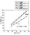
- the hole injection reducing layer 20 is provided up to a distance of 1.1 times or more the plate thickness.
- the formation position of the hole injection reduction layer 20 depends on the thickness of the semiconductor substrate and the impurity concentration of the body p-type region 5c when the impurity concentration of the body p-type region 5c is low, and the impurity concentration of the body p-type region 5c. It was confirmed that when the value of D was increased, the value depended on the thickness of the semiconductor substrate. Specifically, in a structure in which the hole injection reduction layer 20 is not provided, the impurity concentration Pa of the body p-type region 5c is changed to examine how much holes protrude to the IGBT portion 100 side.
- the region in which the IGBT unit 100 has a larger amount of carriers than the diode unit 200 is examined, and how much the protrusion amount L1 from the boundary position between the IGBT unit 100 and the diode unit 200 in the region to the IGBT unit 100 side is determined.
- simulation analysis was performed using the structure shown in FIG. 1 in which the hole injection reduction layer 20 is not provided, and the hole diffusion width was obtained.
- the portion of the IGBT portion 100 where the carrier (hole density) is larger than that of the diode portion 200 is represented as X, and the portion where the carrier is reduced is represented as O.
- the relationship between the ratio of L1 and the plate thickness T1 was examined. As a result, the relationship shown in FIG. 15 was obtained.
- the impurity concentration of the body p-type region 5c is 6 ⁇ 10 15 cm ⁇ 3 or less
- the ratio L1 / T1 of the plate thickness T1 changes. Specifically, as the impurity concentration Pa increases, the lower limit of the ratio L1 / T1 at which the IGBT unit 100 has fewer carriers than the diode unit 200 increases. That is, as the impurity concentration Pa increases, the number of carriers in the IGBT unit 100 does not become less than the number of carriers in the diode unit 200 unless the protrusion amount L1 increases.
- the impurity concentration of the body p-type region 5c is 1 ⁇ 10 ⁇ 16 cm ⁇ 3 or 3 ⁇ 10 ⁇ 16 cm ⁇ 3
- the ratio L1 / T1 between the protrusion amount L1 and the thickness T1 of the semiconductor substrate is 1.
- the protrusion amount L of the hole injection reducing layer 20 is set so as to satisfy the relationship of 1 time or more. That is, the protrusion amount L of the hole injection reducing layer 20 is set so as to be at least the length of the protrusion amount L1 of the hole to the IGBT portion 100 side. Thereby, it is possible to suppress the holes injected from the IGBT unit 100 from affecting the AC loss, and it is possible to further reduce the AC loss.
- the thickness T1 of the semiconductor substrate is 75 ⁇ m and the impurity concentration of the body p-type region 5c is 3 ⁇ 10 15 cm ⁇ 3 , which corresponds to the case of point A in FIG. is doing.
- This condition corresponds to the case where the impurity concentration of the body p-type region 5c is 6 ⁇ 10 15 cm ⁇ 3 or less, and the relationship between the protrusion amount L of the hole injection reducing layer 20 and the plate thickness T1 is the point in FIG. It only has to be A.
- the ratio of the protrusion amount L of the hole injection reducing layer 20 to the plate thickness T1 is 1.1 times or more. It was made to become.
- the relationship of the ratio L / T1 to the change in the impurity concentration of the body p-type region 5c in FIG. Based on the straight line, the protrusion amount L of the hole injection reducing layer 20 may be set. Specifically, in FIG.
- the hole density is low in the thinning portion, so that the hole density on the IGBT portion 100 side is higher than that on the diode portion 200 side. Becomes lower. Therefore, even if the ratio L / T1 between the protrusion amount L of the hole injection reducing layer 20 and the plate thickness T1 is lower than the relationship shown in FIG. 15, the IGBT part 100 can reduce carriers more than the diode part 200. Become.
- the ratio between the protrusion amount L of the hole injection reducing layer 20 and the plate thickness T1 If the ratio is 1.1 times or more, the above-described effect can be obtained even with a structure having a thinning portion.
- the impurity concentration of the hole injection reducing layer 20 may be set higher than the impurity concentration of the n ⁇ type drift layer 1 and the impurity concentration peak value may be set lower than the impurity concentration peak value of the anode region 5b.
- the hole injection reduction layer 20 can be appropriately changed according to the required AC loss and DC loss settings.
- the pitch of the trench 6 of the IGBT part 100 and the diode part 200 is changed, but the same pitch may be used. Moreover, in the IGBT part 100 and the diode part 200, the pitch of the trench 6 does not need to be constant, and there may be different pitches.
- the diode unit 200 may have a structure in which the emitter region 7 and the body p-type region 5c are formed in the p-type region 5 that is the anode region 5b.
- a semiconductor device including an n-channel type IGBT in which the first conductivity type is n-type and the second conductivity type is p-type has been described as an example. It is also possible to use a p-channel type IGBT in which is inverted.
Abstract
This semiconductor device has an IGBT section (100) in which a vertical IGBT is formed, and a diode section (200) which is provided along the IGBT section, and in which a diode is formed. In the diode section, a hole injection reduction layer (20) which has a first type of conduction is provided in the upper layer part of a drift layer (1), the hole injection reduction layer being deeper and having a lower impurity concentration than an anode region (5b) constituted by a second conduction type region (5) in the diode section, as well as having a higher impurity concentration than the drift layer.
Description
本開示は、2013年12月20日に出願された日本出願番号2013-264294号と、2014年12月8日に出願された日本出願番号2014-248139号に基づくもので、ここにその記載内容を援用する。
This disclosure is based on Japanese Application No. 2013-264294 filed on December 20, 2013 and Japanese Application No. 2014-248139 filed on December 8, 2014. Is used.
本開示は、絶縁ゲート型電界効果トランジスタ(以下、IGBTという)とフリーホイールダイオード(以下、単にダイオードという)とが共に1つの基板に形成された半導体装置に関するものである。
The present disclosure relates to a semiconductor device in which both an insulated gate field effect transistor (hereinafter referred to as IGBT) and a free wheel diode (hereinafter simply referred to as a diode) are formed on one substrate.
特許文献1において、インバータなどの回路に備えられるIGBTとダイオードとが並列して備えられた半導体装置が提案されている。特許文献1に示される半導体装置では、次のような手法によってライフタイム制御を行っている。
Patent Document 1 proposes a semiconductor device in which an IGBT and a diode provided in a circuit such as an inverter are provided in parallel. In the semiconductor device disclosed in Patent Document 1, lifetime control is performed by the following method.
具体的には、半導体プロセスを経てIGBTおよびダイオードを共に1つの基板に形成したものを用意する。そして、基板表面側からIGBTおよびダイオードの形成位置にイオン注入を行うと共に、基板裏面側からダイオードの形成位置にイオン注入を行い、さらにアニール処理を行う。これにより、イオン注入が行われた部分に欠陥が形成され、ライフタイム制御を行うことが可能となる。
Specifically, a semiconductor substrate in which an IGBT and a diode are both formed on one substrate is prepared. Then, ion implantation is performed from the substrate surface side to the IGBT and diode formation positions, and ion implantation is performed from the substrate rear surface side to the diode formation positions, followed by annealing. Thereby, a defect is formed in the portion where ion implantation has been performed, and lifetime control can be performed.
しかしながら、特許文献1に記載のライフタイム制御では、イオン注入が行われる位置にトレンチゲート構造を構成するトレンチが存在すると、トレンチ内壁面に形成されたゲート絶縁膜にイオン注入によるダメージを与えてしまう。このダメージは高温度でのアニール処理を行えば回復可能であるが、ライフタイム制御のために形成した欠陥が380℃以上のアニール処理で回復してしまうため、380℃以上のアニール処理を行うことができない。
However, in the lifetime control described in Patent Document 1, if a trench constituting a trench gate structure is present at a position where ion implantation is performed, damage to the gate insulating film formed on the inner wall surface of the trench is caused by ion implantation. . This damage can be recovered by annealing at a high temperature, but defects formed for lifetime control are recovered by annealing at 380 ° C. or higher, so that annealing at 380 ° C. or higher is performed. I can't.
これに対して、従来より、基板裏面側からIGBTおよびダイオードの形成位置の全域にイオン注入を行うことでライフタイム制御を行うことも一般的に行われている。しかしながら、このような手法では、IGBTとダイオードとが同時にライフタイム制御が行われることになり、IGBTとダイオードとのライフタイム制御を個別に最適化して行うことができない。特に、IGBTについては、ライフタイム制御を行うことによる特性劣化が懸念され、ライフタイム制御を最小限に抑える方が好ましい。
In contrast to this, conventionally, lifetime control is generally performed by performing ion implantation from the back side of the substrate to the entire area where the IGBT and the diode are formed. However, in such a method, the lifetime control of the IGBT and the diode is performed simultaneously, and the lifetime control of the IGBT and the diode cannot be individually optimized and performed. In particular, for IGBT, there is a concern about characteristic deterioration due to lifetime control, and it is preferable to minimize lifetime control.
本開示は上記点に鑑みて、ゲート絶縁膜にイオン注入によるダメージを与えることなく、かつ、ライフタイム制御を最小限、好ましくはライフタイム制御を行わなくても、IGBTとダイオードの特性を別々に最適化できる半導体装置を提供することを目的とする。
In view of the above points, the present disclosure provides the characteristics of the IGBT and the diode separately without damaging the gate insulating film by ion implantation and minimizing lifetime control, preferably without performing lifetime control. An object is to provide a semiconductor device that can be optimized.
本開示の一態様に係る半導体装置は、縦型のIGBTが形成されたIGBT部と、前記IGBT部に沿って備えられ、ダイオードが形成されたダイオード部と、を有し、ドリフト層と、コレクタ領域と、カソード領域と、第2導電型領域と、トレンチと、エミッタ領域と、ホール注入低減層と、ゲート絶縁膜と、ゲート電極と、上部電極と、下部電極とを備える。
A semiconductor device according to one embodiment of the present disclosure includes an IGBT portion in which a vertical IGBT is formed, and a diode portion provided along the IGBT portion and in which a diode is formed, a drift layer, a collector The region includes a region, a cathode region, a second conductivity type region, a trench, an emitter region, a hole injection reducing layer, a gate insulating film, a gate electrode, an upper electrode, and a lower electrode.
前記ドリフト層は第1導電型を有する。前記コレクタ領域は第2導電型を有し、前記IGBT部において、前記ドリフト層の裏面側に形成される。前記カソード領域は第1導電型を有し、前記ダイオード部において、前記ドリフト層の裏面側に形成される。前記第2導電型領域は、前記ドリフト層の表面側の表層部において、前記IGBT部および前記ダイオード部の双方に形成される。前記トレンチは、前記IGBT部において、複数本並べられ、前記第2導電型領域よりも深く形成されて前記第2導電型領域を複数に分けることで、前記第2導電型領域の少なくとも一部によってチャネル領域を構成する。前記エミッタ領域は、第1導電型を有し、前記IGBT部において、前記チャネル領域の表層部に前記トレンチの側面に沿って形成される。前記ホール注入低減層は第1導電型を有し、前記ダイオード部において前記ドリフト層の上層部に形成され、前記ダイオード部における前記第2導電型領域により構成されるアノード領域よりも深くて低不純物濃度とされ、かつ、前記ドリフト層よりも高不純物濃度とされる。前記ゲート絶縁膜は、前記トレンチの表面に形成される。前記ゲート電極は、前記ゲート絶縁膜の表面に形成される。前記上部電極は、前記IGBT部において前記第2導電型領域に電気的に接続されると共に、前記アノード領域に電気的に接続される。前記下部電極は、前記IGBT部において前記コレクタ領域に電気的に接続されると共に、前記ダイオード部において前記カソード領域と電気的に接続される。
The drift layer has the first conductivity type. The collector region has a second conductivity type, and is formed on the back surface side of the drift layer in the IGBT portion. The cathode region has a first conductivity type, and is formed on the back side of the drift layer in the diode portion. The second conductivity type region is formed in both the IGBT part and the diode part in the surface layer part on the surface side of the drift layer. A plurality of the trenches are arranged in the IGBT portion, are formed deeper than the second conductivity type region, and divide the second conductivity type region into a plurality of parts, so that at least a part of the second conductivity type region is formed. Configure the channel region. The emitter region has a first conductivity type, and is formed along a side surface of the trench in a surface layer portion of the channel region in the IGBT portion. The hole injection reducing layer has a first conductivity type, is formed in an upper layer portion of the drift layer in the diode portion, and is deeper and less impurity than an anode region constituted by the second conductivity type region in the diode portion. The impurity concentration is higher than that of the drift layer. The gate insulating film is formed on the surface of the trench. The gate electrode is formed on the surface of the gate insulating film. The upper electrode is electrically connected to the second conductivity type region in the IGBT portion and electrically connected to the anode region. The lower electrode is electrically connected to the collector region in the IGBT portion and electrically connected to the cathode region in the diode portion.
前記半導体装置は、前記ダイオード部に前記ホール注入低減層を備えている。このため、前記IGBTの動作中に前記ダイオード部を通じて注入されるホールを低減することが可能となる。これにより、スイッチング時のAC損失を低減することが可能となる。また、前記ホール注入低減層の不純物濃度に応じて、AC損失やAC損失とトレードオフの関係となるDC損失について調整できる。したがって、前記ダイオード部に前記ホール注入低減層を備えることによって、AC損失とDC損失を最適に設定できることから、前記IGBTと前記ダイオードの特性を別々に最適化することが可能となる。
The semiconductor device includes the hole injection reducing layer in the diode portion. For this reason, it becomes possible to reduce the holes injected through the diode part during the operation of the IGBT. As a result, AC loss during switching can be reduced. Further, AC loss and DC loss that is in a trade-off relationship with AC loss can be adjusted according to the impurity concentration of the hole injection reducing layer. Therefore, by providing the hole injection reducing layer in the diode portion, AC loss and DC loss can be set optimally, so that the characteristics of the IGBT and the diode can be optimized separately.
本開示における上記あるいは他の目的、構成、利点は、下記の図面を参照しながら、以下の詳細説明から、より明白となる。図面において、
図1は、本開示の第1実施形態にかかるIGBTとダイオードを備えた半導体装置の断面図である。
図2は、p型領域とホール注入低減層の不純物濃度分布を示した図である。
図3は、IGBTのオフ時にコレクタ電流Icの変化を測定した結果を示した図である。
図4は、ホール注入低減層の不純物濃度ピークを変化させたときの各濃度分布を示した図である。
図5は、ホール注入低減層の不純物濃度ピークを変化させたときのAC損失とDC損失について調べた結果を示す図である。
図6は、ホール注入低減層が備えられた第1実施形態の構造と備えられていない従来構造それぞれについてAC損失とDC損失の関係について調べた結果を示す図である。
図7は、本開示の第2実施形態にかかるIGBTとダイオードを備えた半導体装置の断面図である。
図8は、本開示の第3実施形態にかかるIGBTとダイオードを備えた半導体装置の断面図である。
図9は、IGBT部にホール注入低減層を形成していない場合におけるホール分布を示す図である。
図10は、ホール注入低減層のはみ出し量を変化させた場合のAC損失とDC損失とを調べた結果を示す図である。
図11は、ホール注入低減層のはみ出し量を変化させた場合のダイオード部での全損失を調べた結果を示す図である。
図12は、本開示の第4実施形態にかかるIGBTとダイオードを備えた半導体装置の断面図である。
図13は、本開示の第5実施形態にかかるIGBTとダイオードを備えた半導体装置の断面図である。
図14は、IGBT部にホール注入低減層を形成していない場合におけるホール分布とIGBT部とダイオード部のホール密度の比較結果を示した図である。
図15は、ボディp型領域の不純物濃度の変化に対するはみ出し量L1と板厚T1との比L1/T1の関係を示した図である。
図16は、板厚T1とホール拡散長との関係をボディp型領域の不純物濃度を変えて調べた結果を示す図である。
The above and other objects, configurations, and advantages of the present disclosure will become more apparent from the following detailed description with reference to the following drawings. In the drawing
FIG. 1 is a cross-sectional view of a semiconductor device including an IGBT and a diode according to the first embodiment of the present disclosure. FIG. 2 is a diagram showing the impurity concentration distribution of the p-type region and the hole injection reduction layer. FIG. 3 is a diagram showing a result of measuring a change in the collector current Ic when the IGBT is turned off. FIG. 4 is a diagram showing each concentration distribution when the impurity concentration peak of the hole injection reducing layer is changed. FIG. 5 is a diagram showing the results of examining the AC loss and DC loss when the impurity concentration peak of the hole injection reducing layer is changed. FIG. 6 is a diagram showing the results of examining the relationship between AC loss and DC loss for each of the structure of the first embodiment provided with the hole injection reducing layer and the conventional structure not provided. FIG. 7 is a cross-sectional view of a semiconductor device including an IGBT and a diode according to the second embodiment of the present disclosure. FIG. 8 is a cross-sectional view of a semiconductor device including an IGBT and a diode according to the third embodiment of the present disclosure. FIG. 9 is a diagram showing a hole distribution when a hole injection reducing layer is not formed in the IGBT portion. FIG. 10 is a diagram showing the results of examining AC loss and DC loss when the amount of protrusion of the hole injection reducing layer is changed. FIG. 11 is a diagram showing the result of examining the total loss in the diode portion when the amount of protrusion of the hole injection reducing layer is changed. FIG. 12 is a cross-sectional view of a semiconductor device including an IGBT and a diode according to the fourth embodiment of the present disclosure. FIG. 13 is a cross-sectional view of a semiconductor device including an IGBT and a diode according to the fifth embodiment of the present disclosure. FIG. 14 is a diagram showing a comparison result of the hole distribution and the hole density of the IGBT part and the diode part when the hole injection reducing layer is not formed in the IGBT part. FIG. 15 is a diagram showing the relationship of the ratio L1 / T1 between the protrusion amount L1 and the plate thickness T1 with respect to the change in the impurity concentration in the body p-type region. FIG. 16 is a diagram showing the results of examining the relationship between the plate thickness T1 and the hole diffusion length by changing the impurity concentration in the body p-type region.
以下、本開示の実施形態について図に基づいて説明する。なお、以下の各実施形態相互において、互いに同一もしくは均等である部分には、同一符号を付して説明を行う。
Hereinafter, embodiments of the present disclosure will be described with reference to the drawings. In the following embodiments, parts that are the same or equivalent to each other will be described with the same reference numerals.
(第1実施形態)
本開示の第1実施形態について説明する。図1に示すように、本実施形態にかかる半導体装置は、基板厚み方向に電流を流す縦型のIGBTとダイオードとが1つの基板に備えられることにより構成されている。具体的には、本実施形態にかかる半導体装置は以下のように構成されている。 (First embodiment)
A first embodiment of the present disclosure will be described. As shown in FIG. 1, the semiconductor device according to the present embodiment is configured by providing a vertical IGBT and a diode that allow current to flow in the substrate thickness direction on one substrate. Specifically, the semiconductor device according to the present embodiment is configured as follows.
図1に示されるように、本実施形態にかかる半導体装置は、IGBTが備えられるIGBT部100と、IGBT部100に沿って備えられ、ダイオードが形成されたダイオード部200とを有した構成とされている。これらIGBT部100やダイオード部200は、例えばチップの中央部のセル領域に形成されており、セル領域の外周、つまりチップの外縁部に図示しない外周耐圧部が配置されることにより、本実施形態にかかる半導体装置が構成されている。
As shown in FIG. 1, the semiconductor device according to the present embodiment includes an IGBT unit 100 provided with an IGBT, and a diode unit 200 provided along the IGBT unit 100 and formed with a diode. ing. The IGBT unit 100 and the diode unit 200 are formed, for example, in a cell region in the center of the chip, and an outer peripheral pressure-resistant unit (not shown) is arranged on the outer periphery of the cell region, that is, on the outer edge of the chip. The semiconductor device concerning this is comprised.
IGBTおよびダイオードは、n-型ドリフト層1を構成する半導体基板を用いて形成されている。IGBT部100およびダイオード部200において、n-型ドリフト層1の裏面側におけるn-型ドリフト層1の表層部には、n型層によって構成されるフィールドストップ(以下、FSという)層2が形成されている。FS層2は、n-型ドリフト層1の裏面から比較的浅い所定深さの位置まで形成され、リン(P)などのn型不純物が注入されることで構成されている。FS層2の不純物濃度や拡散深さについては、要求されるIGBTやダイオードの特性に応じて設定されている。
The IGBT and the diode are formed using a semiconductor substrate constituting the n − type drift layer 1. In IGBT portion 100 and diode portion 200, a field stop (hereinafter referred to as FS) layer 2 composed of an n-type layer is formed on the surface layer portion of n − -type drift layer 1 on the back surface side of n − -type drift layer 1. Has been. The FS layer 2 is formed from the back surface of the n − -type drift layer 1 to a relatively shallow position of a predetermined depth, and is configured by implanting an n-type impurity such as phosphorus (P). The impurity concentration and diffusion depth of the FS layer 2 are set according to the required characteristics of the IGBT and diode.
IGBT部100において、FS層2の表層部に、p+型不純物層にて構成されたコレクタ領域3が形成されている。コレクタ領域3は、ボロン等のp型不純物が注入されて形成されている。また、ダイオード部200において、FS層2の表層部に、n+型不純物層にて構成されたカソード領域4が形成されている。カソード領域4は、リン等のn型不純物が注入されて形成されている。これらコレクタ領域3やカソード領域4の不純物濃度や拡散深さについては、要求されるIGBTやダイオードの特性に応じて設定されている。
In the IGBT portion 100, a collector region 3 composed of ap + -type impurity layer is formed in the surface layer portion of the FS layer 2. The collector region 3 is formed by implanting p-type impurities such as boron. In the diode portion 200, a cathode region 4 composed of an n + -type impurity layer is formed in the surface layer portion of the FS layer 2. The cathode region 4 is formed by implanting n-type impurities such as phosphorus. The impurity concentration and diffusion depth of the collector region 3 and the cathode region 4 are set according to the required characteristics of the IGBT and the diode.
さらに、IGBT部100およびダイオード部200の両方において、n-型ドリフト層1の表面側の表層部にp型領域5が形成されている。このp型領域5を貫通してn-型ドリフト層1まで達するように複数個のトレンチ6が形成されており、このトレンチ6によってp型領域5が複数個に分離されている。具体的には、トレンチ6は複数個所定のピッチ(間隔)で形成されており、図1の紙面垂直方向において各トレンチ6が平行に延設されたストライプ構造、もしくは並行に延設されたのちその先端部において引き回されることで環状構造とされている。環状構造とされる場合、例えば各トレンチ6が構成する環状構造は複数本ずつを1組として多重リング構造が構成される。
Further, in both IGBT portion 100 and diode portion 200, p type region 5 is formed in the surface layer portion on the surface side of n − type drift layer 1. A plurality of trenches 6 are formed so as to penetrate the p-type region 5 and reach the n − -type drift layer 1, and the p-type region 5 is separated into a plurality of trenches 6. Specifically, a plurality of trenches 6 are formed at a predetermined pitch (interval), and a stripe structure in which the trenches 6 extend in parallel in the direction perpendicular to the paper surface of FIG. An annular structure is formed by being drawn around the tip. In the case of an annular structure, for example, a plurality of annular structures formed by each trench 6 constitute a multiple ring structure.
トレンチ6によって複数に分割されたp型領域5のうち、IGBT部100に形成された部分は、チャネル領域を構成するチャネルp型領域5aとなる。このチャネルp型領域5aの表層部に、n+型不純物層にて構成されたエミッタ領域7が形成されている。
Of the p-type region 5 divided into a plurality of portions by the trench 6, a portion formed in the IGBT portion 100 becomes a channel p-type region 5 a constituting the channel region. In the surface layer portion of the channel p-type region 5a, an emitter region 7 composed of an n + -type impurity layer is formed.
p型領域5のうち、チャネルp型領域5aの表層部、具体的にはチャネルp型領域5a内の両側に配置されたエミッタ領域7の間に、チャネルp型領域5aのコンタクト部としても機能する高濃度なボディp型領域5cが形成されている。このため、IGBT部100ではp型領域5のp型不純物濃度の表面濃度が高濃度とされている。
Of the p-type region 5, it also functions as a contact portion of the channel p-type region 5 a between the surface layer portion of the channel p-type region 5 a, specifically between the emitter regions 7 arranged on both sides in the channel p-type region 5 a. A high-concentration body p-type region 5c is formed. For this reason, in the IGBT portion 100, the surface concentration of the p-type impurity concentration of the p-type region 5 is set high.
エミッタ領域7は、n-型ドリフト層1よりも高不純物濃度で構成され、p型領域5内において終端しており、かつ、トレンチ6の側面に接するように配置されている。より詳しくは、トレンチ6の長手方向に沿って棒状に延設され、トレンチ6の先端よりも内側で終端した構造とされている。
The emitter region 7 has a higher impurity concentration than the n − type drift layer 1, terminates in the p-type region 5, and is disposed so as to be in contact with the side surface of the trench 6. More specifically, the structure extends in the shape of a rod along the longitudinal direction of the trench 6 and terminates inside the tip of the trench 6.
トレンチ6は、p型領域5よりも深くされており、上述したように図1に示す断面において所定のピッチで配置されている。また、各トレンチ6内は、各トレンチ6の内壁表面を覆うように形成されたゲート絶縁膜8と、このゲート絶縁膜8の表面に形成されたドープトPoly-Si等により構成されるゲート電極9とにより埋め込まれている。IGBT部100に形成されたゲート電極9は、図1とは別断面において互いに電気的に接続され、同電位のゲート電圧が印加されるようになっている。
The trenches 6 are deeper than the p-type region 5 and are arranged at a predetermined pitch in the cross section shown in FIG. 1 as described above. In each trench 6, a gate insulating film 8 formed so as to cover the inner wall surface of each trench 6, and a gate electrode 9 constituted by doped Poly-Si or the like formed on the surface of the gate insulating film 8. And embedded by. The gate electrodes 9 formed in the IGBT section 100 are electrically connected to each other in a cross section different from that in FIG. 1 and are applied with a gate voltage having the same potential.
さらに、エミッタ領域7およびチャネルp型領域5aは、層間絶縁膜10に形成されたコンタクトホール10aを通じて、エミッタ電極を構成する上部電極11と電気的に接続されている。また、図示しないが、上部電極11や配線などを保護するようにパッシベーション膜が形成されている。そして、コレクタ領域3の裏面側にコレクタ電極を構成する下部電極12が形成されることにより、IGBTが構成されている。
Furthermore, the emitter region 7 and the channel p-type region 5a are electrically connected to the upper electrode 11 constituting the emitter electrode through a contact hole 10a formed in the interlayer insulating film 10. Although not shown, a passivation film is formed so as to protect the upper electrode 11 and the wiring. Then, the lower electrode 12 constituting the collector electrode is formed on the back surface side of the collector region 3, whereby the IGBT is constituted.
トレンチ6によって複数に分割されたp型領域5のうち、ダイオード部200に形成された部分は、アノード領域5bとされ、表層部が比較的高濃度とされることでコンタクト領域が構成されている。上記した上部電極11はダイオード部200にも延設されており、アノード領域5bにオーミック接続されることでアノード電極としても機能する。さらに、上記した下部電極12もダイオード部200まで延設されており、カソード領域4にオーミック接触されられることでカソード電極としても機能する。このような構成により、ダイオードが構成されている。
そして、本実施形態では、上記のように構成されたダイオード部200にn型層にて構成されたホール注入低減層20が備えられている。ホール注入低減層20は、n-型ドリフト層1の上層部において、アノード領域5bからのホールの注入を低減させる役割を果たし、アノード領域5bよりも深く、かつ、トレンチ6の底部よりも浅い位置に形成されている。ホール注入低減層20の不純物濃度は、n-型ドリフト層1の不純物濃度よりも濃く、かつ、図2に示すように、不純物濃度ピーク値がアノード領域5bの不純物濃度ピーク値よりも低く設定されている。例えば、n-型ドリフト層1の不純物濃度が7×10¹³~8×1014cm-3、ホール注入低減層20の不純物濃度が1×10¹⁶~1×1017cm-3、アノード領域5bの不純物濃度が1×1017cm-3以上に設定される。ホール注入低減層20の厚みについては任意であるが、例えば1~2μmとされている。 Of the p-type region 5 divided into a plurality of portions by the trench 6, a portion formed in the diode portion 200 is an anode region 5b, and a contact region is formed by making the surface layer portion have a relatively high concentration. . The above-described upper electrode 11 is also extended to the diode part 200, and functions as an anode electrode by being ohmically connected to the anode region 5b. Further, the lower electrode 12 described above also extends to the diode portion 200 and functions as a cathode electrode by being in ohmic contact with the cathode region 4. With such a configuration, a diode is configured.
In the present embodiment, thediode portion 200 configured as described above is provided with the hole injection reducing layer 20 formed of an n-type layer. The hole injection reduction layer 20 plays a role of reducing hole injection from the anode region 5 b in the upper layer portion of the n − -type drift layer 1, and is deeper than the anode region 5 b and shallower than the bottom of the trench 6. Is formed. The impurity concentration of the hole injection reducing layer 20 is higher than the impurity concentration of the n − type drift layer 1, and the impurity concentration peak value is set lower than the impurity concentration peak value of the anode region 5b as shown in FIG. ing. For example, the impurity concentration of the n − type drift layer 1 is 7 × 10 13 to 8 × 10 14 cm −3 , the impurity concentration of the hole injection reducing layer 20 is 1 × 10 16 to 1 × 10 17 cm −3 , and the anode region 5b. Is set to 1 × 10 17 cm −3 or more. The thickness of the hole injection reducing layer 20 is arbitrary, but is, for example, 1 to 2 μm.
そして、本実施形態では、上記のように構成されたダイオード部200にn型層にて構成されたホール注入低減層20が備えられている。ホール注入低減層20は、n-型ドリフト層1の上層部において、アノード領域5bからのホールの注入を低減させる役割を果たし、アノード領域5bよりも深く、かつ、トレンチ6の底部よりも浅い位置に形成されている。ホール注入低減層20の不純物濃度は、n-型ドリフト層1の不純物濃度よりも濃く、かつ、図2に示すように、不純物濃度ピーク値がアノード領域5bの不純物濃度ピーク値よりも低く設定されている。例えば、n-型ドリフト層1の不純物濃度が7×10¹³~8×1014cm-3、ホール注入低減層20の不純物濃度が1×10¹⁶~1×1017cm-3、アノード領域5bの不純物濃度が1×1017cm-3以上に設定される。ホール注入低減層20の厚みについては任意であるが、例えば1~2μmとされている。 Of the p-
In the present embodiment, the
なお、本実施形態では、ホール注入低減層20の底部がトレンチ6の底部よりも浅くなる構成としたが、トレンチ6の底部よりも深くなる構成であっても構わない。
In the present embodiment, the bottom of the hole injection reducing layer 20 is shallower than the bottom of the trench 6, but may be deeper than the bottom of the trench 6.
以上のようにして、本実施形態にかかるIGBTおよびダイオードを備えた半導体装置が構成されている。このように構成された半導体装置では、ダイオード部200にホール注入低減層20が備えられている。このため、IGBT動作中にダイオード部200を通じて注入されるホールを低減することが可能となる。これにより、IGBTのオフ時に引き抜かなければならないホール量を少なくすることが可能となって、図3に示すように、IGBTのオフ時にコレクタ電流Icが0になるときに、0を下回ってオーバーシュートするときの突き出し量が小さくなる。よって、スイッチング時のAC損失を低減することが可能となる。
As described above, the semiconductor device including the IGBT and the diode according to the present embodiment is configured. In the semiconductor device configured as described above, the hole injection reduction layer 20 is provided in the diode portion 200. For this reason, it is possible to reduce holes injected through the diode part 200 during the IGBT operation. This makes it possible to reduce the amount of holes that must be extracted when the IGBT is turned off. As shown in FIG. 3, when the collector current Ic becomes 0 when the IGBT is turned off, the overshoot falls below 0. The amount of protrusion when doing this is small. Therefore, AC loss during switching can be reduced.
ホール注入量についてはホール注入低減層20の濃度を濃くすればするほど少なくなることから、ホール注入低減層20の不純物濃度ピークを高くすることで、よりAC損失を低減することが可能となる。ただし、スイッチング時のDC損失についてはAC損失とトレードオフの関係となっており、ホール注入低減層20の不純物濃度ピークが高くなるほど、DC損失が大きくなる。例えば、図4に示すように、ホール注入低減層20の不純物濃度ピークを4段階に変化させて、AC損失とDC損失の関係について調べたところ、図5に示す関係が得られた。
Since the hole injection amount decreases as the concentration of the hole injection reduction layer 20 is increased, the AC loss can be further reduced by increasing the impurity concentration peak of the hole injection reduction layer 20. However, the DC loss at the time of switching has a trade-off relationship with the AC loss, and the DC loss increases as the impurity concentration peak of the hole injection reduction layer 20 increases. For example, as shown in FIG. 4, the relationship between AC loss and DC loss was examined by changing the impurity concentration peak of the hole injection reducing layer 20 in four stages, and the relationship shown in FIG. 5 was obtained.
このように、AC損失とDC損失にはトレードオフの関係が有り、これらをホール注入低減層20の不純物濃度ピークに応じて調整できる。このため、要求される仕様に応じてホール注入低減層20の不純物濃度ピークを設定すれば、AC損失とDC損失を最適に設定できる。そして、ダイオード部200にホール注入低減層20を備えることによって、AC損失とDC損失を最適に設定できることから、IGBTとダイオードの特性を別々に最適化することが可能となる。
Thus, there is a trade-off relationship between AC loss and DC loss, and these can be adjusted according to the impurity concentration peak of the hole injection reducing layer 20. For this reason, AC loss and DC loss can be optimally set by setting the impurity concentration peak of the hole injection reducing layer 20 in accordance with the required specifications. And, by providing the hole injection reducing layer 20 in the diode part 200, AC loss and DC loss can be set optimally, so that the characteristics of the IGBT and the diode can be optimized separately.
また、本実施形態のようにホール注入低減層20が備えられた構造と備えられていない従来構造それぞれについてAC損失とDC損失の関係について調べたところ、図6に示す結果が得られた。このように、本実施形態の構造の方が従来構造と比較してAC損失を同じ値とした場合のDC損失が改善されており、半導体装置の性能が向上できていることが判る。したがって、本実施形態のように、ホール注入低減層20を備えることにより、半導体装置の性能向上を図ることが可能となる。
Further, when the relationship between the AC loss and the DC loss was examined for each of the structure provided with the hole injection reducing layer 20 and the conventional structure not provided as in the present embodiment, the result shown in FIG. 6 was obtained. Thus, it can be seen that the structure of this embodiment has improved DC loss when the AC loss is the same as that of the conventional structure, and the performance of the semiconductor device can be improved. Therefore, it is possible to improve the performance of the semiconductor device by providing the hole injection reducing layer 20 as in this embodiment.
続いて、このように構成される半導体装置の製造方法について説明する。ただし、本実施形態のような構造の半導体装置については、従来構造の半導体装置とほぼ同様の製造方法によって製造可能であるため、従来と異なる部分について主に説明する。
Subsequently, a manufacturing method of the semiconductor device configured as described above will be described. However, since the semiconductor device having the structure as in the present embodiment can be manufactured by a manufacturing method almost the same as that of the semiconductor device having the conventional structure, portions different from the conventional one will be mainly described.
まず、n-型ドリフト層1を構成する半導体基板を用意したのち、ダイオード部200におけるホール注入低減層20の形成位置にn型不純物をイオン注入する。また、IGBT部100およびダイオード部200において、n-型ドリフト層1の表層部にp型領域5の形成のためにp型不純物をイオン注入する。さらに、IGBT部100におけるボディp型領域5cやエミッタ領域7の形成位置にそれぞれp型不純物とn型不純物をイオン注入する。そして、アニール処理による熱拡散工程を行うことで、注入したイオンを熱拡散させ、ホール注入低減層20、p型領域5、ボディp型領域5cおよびエミッタ領域7を形成する。
First, after preparing a semiconductor substrate constituting the n − -type drift layer 1, n-type impurities are ion-implanted into the formation position of the hole injection reducing layer 20 in the diode portion 200. In IGBT portion 100 and diode portion 200, p-type impurities are ion-implanted in the surface layer portion of n − -type drift layer 1 in order to form p-type region 5. Further, p-type impurities and n-type impurities are ion-implanted into the formation positions of the body p-type region 5 c and the emitter region 7 in the IGBT portion 100, respectively. Then, by performing a thermal diffusion process by annealing, the implanted ions are thermally diffused to form the hole injection reducing layer 20, the p-type region 5, the body p-type region 5c, and the emitter region 7.
次に、IGBT部100およびダイオード部200において、トレンチゲート構造の形成予定位置が開口するマスク(図示せず)を配置したのち、異方性エッチングを行うことでトレンチ6を形成する。その後、熱酸化によるゲート絶縁膜8の形成工程、ドープトポリシリコンの成膜およびパターニングによるゲート電極9の形成工程を行う。そして、層間絶縁膜10を形成した後、コンタクトホール10aの形成工程を行い、さらにAlなどの電極材料をパターニングして上部電極11を形成する。これにより、基板表面側の製造工程が終了する。
Next, in the IGBT part 100 and the diode part 200, a mask (not shown) having an opening where a trench gate structure is to be formed is disposed, and then the trench 6 is formed by performing anisotropic etching. Thereafter, a step of forming a gate insulating film 8 by thermal oxidation, a step of forming a gate electrode 9 by film formation and patterning of doped polysilicon are performed. And after forming the interlayer insulation film 10, the formation process of the contact hole 10a is performed, Furthermore, electrode materials, such as Al, are patterned, and the upper electrode 11 is formed. Thereby, the manufacturing process on the substrate surface side is completed.
続いて、n-型ドリフト層1を構成する半導体基板の裏面側を所望厚さとなるまで研削してから必要に応じてエッチングして表面平坦化を行する。その後、FS層2の形成のためのリンのイオン注入、コレクタ領域3の形成のためのボロンのイオン注入およびカソード領域4の形成のためのリンのイオン注入を行う。そして、レーザアニール等によって表面側に影響を与えない局所的な熱処理を行い、注入されたイオンの拡散工程を行う。更に、Alなどの電極材料を成膜するなどの下部電極12の形成工程を行う。これにより、基板裏面側の製造工程が終了し、図1に示したIGBTおよびダイオードを備えた半導体装置が完成する。
Subsequently, the back surface side of the semiconductor substrate constituting the n − type drift layer 1 is ground to a desired thickness, and then etched as necessary to flatten the surface. Thereafter, phosphorus ion implantation for forming the FS layer 2, boron ion implantation for forming the collector region 3, and phosphorus ion implantation for forming the cathode region 4 are performed. Then, a local heat treatment that does not affect the surface side is performed by laser annealing or the like, and a diffusion process of implanted ions is performed. Further, a process of forming the lower electrode 12 such as forming an electrode material such as Al is performed. Thereby, the manufacturing process on the back surface side of the substrate is completed, and the semiconductor device including the IGBT and the diode shown in FIG. 1 is completed.
このような製造方法においては、ホール注入低減層20を備えることによってダイオードの特性をIGBTの特性と切り離して個別に最適化できる。このため、上記の製造方法においては、トレンチゲート構造を形成してから基板表面側からライフタイム制御のためのイオン注入を行う必要がなくなる。したがって、ゲート絶縁膜8にイオン注入によるダメージを与えることなく、かつ、ライフタイム制御を最小限、好ましくはライフタイム制御を行わなくても、IGBTとダイオードの特性を別々に最適化することが可能となる。
In such a manufacturing method, by providing the hole injection reduction layer 20, the characteristics of the diode can be optimized separately from the characteristics of the IGBT. Therefore, in the above manufacturing method, it is not necessary to perform ion implantation for lifetime control from the substrate surface side after forming the trench gate structure. Therefore, it is possible to optimize the characteristics of the IGBT and the diode separately without damaging the gate insulating film 8 by ion implantation and minimizing lifetime control, preferably without performing lifetime control. It becomes.
(第2実施形態)
本開示の第2実施形態について説明する。本実施形態は、第1実施形態に対してIGBT部100の構成を変更したものであり、その他については第1実施形態と同様であるため、第1実施形態と異なる部分についてのみ説明する。 (Second Embodiment)
A second embodiment of the present disclosure will be described. In the present embodiment, the configuration of theIGBT unit 100 is changed with respect to the first embodiment, and the other parts are the same as those in the first embodiment. Therefore, only different parts from the first embodiment will be described.
本開示の第2実施形態について説明する。本実施形態は、第1実施形態に対してIGBT部100の構成を変更したものであり、その他については第1実施形態と同様であるため、第1実施形態と異なる部分についてのみ説明する。 (Second Embodiment)
A second embodiment of the present disclosure will be described. In the present embodiment, the configuration of the
図7に示すように、本実施形態では、IGBT部100において、隣接するトレンチ6によって複数に分割されたp型領域5の一部のみをチャネルp型領域5aとしている。つまり、p型領域5の一部のみにn+型不純物にて構成されたエミッタ領域7を形成している。このエミッタ領域7が形成された部分がチャネルp型領域5aとされることでIGBT動作させられるIGBT動作部となる。また、p型領域5のうちのエミッタ領域7が形成されない残りの部分は間引き部となり、IGBT動作は行われないようになっている。
As shown in FIG. 7, in the present embodiment, in the IGBT unit 100, only a part of the p-type region 5 divided into a plurality by the adjacent trenches 6 is used as the channel p-type region 5a. That is, the emitter region 7 composed of the n + -type impurity is formed only in a part of the p-type region 5. The portion where the emitter region 7 is formed is the channel p-type region 5a, thereby forming an IGBT operation portion that is allowed to perform an IGBT operation. Further, the remaining part of the p-type region 5 where the emitter region 7 is not formed becomes a thinned-out portion, so that the IGBT operation is not performed.
このように、IGBT部100の全域をIGBT動作部とせずに、部分的に間引き部が備えられた構成とされていても、ダイオード部200について第1実施形態と同様の構造とすることができる。このような構成としても、第1実施形態と同様の効果を得ることができる。
As described above, the diode unit 200 can have the same structure as that of the first embodiment even if the thinned unit is partially provided without using the entire IGBT unit 100 as the IGBT operating unit. . Even with such a configuration, the same effect as in the first embodiment can be obtained.
(第3実施形態)
本開示の第3実施形態について説明する。本実施形態は、第1、第2実施形態に対してホール注入低減層20の形成位置を増加させたものであり、その他については第1、第2実施形態と同様であるため、第1、第2実施形態と異なる部分についてのみ説明する。なお、ここでは第2実施形態に対してホール注入低減層20の形成位置を増加させた場合について説明するが、第1実施形態に対しても同様の構成を適用できる。 (Third embodiment)
A third embodiment of the present disclosure will be described. In the present embodiment, the formation position of the holeinjection reducing layer 20 is increased with respect to the first and second embodiments, and the others are the same as those in the first and second embodiments. Only parts different from the second embodiment will be described. Although the case where the formation position of the hole injection reducing layer 20 is increased with respect to the second embodiment will be described here, the same configuration can be applied to the first embodiment.
本開示の第3実施形態について説明する。本実施形態は、第1、第2実施形態に対してホール注入低減層20の形成位置を増加させたものであり、その他については第1、第2実施形態と同様であるため、第1、第2実施形態と異なる部分についてのみ説明する。なお、ここでは第2実施形態に対してホール注入低減層20の形成位置を増加させた場合について説明するが、第1実施形態に対しても同様の構成を適用できる。 (Third embodiment)
A third embodiment of the present disclosure will be described. In the present embodiment, the formation position of the hole
図8に示すように、本実施形態では、第2実施形態と同様、p型領域5の一部が間引き部とされているのに加え、IGBT部100のうちダイオード部200の近傍に位置する部分にもホール注入低減層20を備えた構造としている。つまり、ホール注入低減層20をIGBT部100側にはみ出すように形成している。具体的には、IGBT部100のうち、ダイオード部200との境界位置から60μm以上の位置までホール注入低減層20を備えている。
As shown in FIG. 8, in the present embodiment, as in the second embodiment, a part of the p-type region 5 is a thinned-out portion and is located in the vicinity of the diode portion 200 in the IGBT portion 100. The portion is also provided with a hole injection reduction layer 20. That is, the hole injection reducing layer 20 is formed so as to protrude to the IGBT part 100 side. Specifically, the hole injection reducing layer 20 is provided from the boundary position with the diode part 200 to a position of 60 μm or more in the IGBT part 100.
第1実施形態のようにIGBT部100にホール注入低減層20を形成していない場合におけるホール分布、すなわちp型領域5の表面から10μmの深さでのホール濃度を調べると、図9に示される結果となった。ここでの実験では、半導体基板の板厚、つまり各拡散層を形成する前の状態におけるn-型ドリフト層1の厚み(各拡散層の形成後におけるn-型ドリフト層1、コレクタ領域3、チャネルp型領域5a、エミッタ領域7のトータルの厚み)を75μmとした。また、ボディp型領域5cの不純物濃度(ピーク値)を3×1015cm-3とした。この図より、IGBT部100の中でもダイオード部200の近傍に位置している部分においてホール密度が高まっていることが判る。
When the hole distribution in the case where the hole injection reducing layer 20 is not formed in the IGBT portion 100 as in the first embodiment, that is, the hole concentration at a depth of 10 μm from the surface of the p-type region 5, is shown in FIG. As a result. In the experiment here, the thickness of the semiconductor substrate, that is, the thickness of the n − type drift layer 1 before the formation of each diffusion layer (the n − type drift layer 1, collector region 3, The total thickness of the channel p-type region 5a and the emitter region 7) was 75 μm. Further, the impurity concentration (peak value) of the body p-type region 5c was set to 3 × 10 15 cm −3 . From this figure, it can be seen that the hole density is increased in a portion of the IGBT portion 100 located in the vicinity of the diode portion 200.
上記したように、ダイオード部200にホール注入低減層20を形成することによってIGBT動作中にダイオード部200を通じて注入されるホールを低減させ、スイッチング時のAC損失を低減させることが可能となる。しかしながら、実際にはIGBT部100から注入されるホールもAC損失に影響を与え、特にIGBT部100の中でもダイオード部200の近傍に位置する部分からのホール注入が大きな影響を与える。
As described above, by forming the hole injection reducing layer 20 in the diode part 200, it is possible to reduce holes injected through the diode part 200 during the IGBT operation and to reduce AC loss during switching. However, in fact, holes injected from the IGBT unit 100 also affect the AC loss, and hole injection from a portion located in the vicinity of the diode unit 200 in the IGBT unit 100 has a great effect.
このため、本実施形態では、ダイオード部200よりもホール密度が高くなっている部分、つまりIGBT部100のうち少なくともダイオード部200との境界位置から60μmの位置までホール注入低減層20を形成している。これにより、IGBT部100から注入されるホールがAC損失に影響を与えることを抑制することが可能となり、よりAC損失の低減を図ることが可能となる。
For this reason, in the present embodiment, the hole injection reducing layer 20 is formed from the portion where the hole density is higher than that of the diode portion 200, that is, at least 60 μm from the boundary position with the diode portion 200 in the IGBT portion 100. Yes. Thereby, it is possible to suppress the holes injected from the IGBT unit 100 from affecting the AC loss, and it is possible to further reduce the AC loss.
なお、参考として、ホール注入低減層20のはみ出し量を変化させた場合のAC損失とDC損失とを調べると共に、ダイオード部200での全損失を調べた。その結果、図10および図11に示す結果が得られた。図10に示す結果から、はみ出し量が大きくなる程(はみ出し量1<はみ出し量2<はみ出し量3)、性能向上が図れていた。ただし、図11に示すように、はみ出し量が一定量に至ると、ダイオード部200での全損失がほぼ一定値に収まっていた。このことから、ホール注入低減層20をIGBT部100の一部にはみ出すように形成することで、半導体装置の更なる性能向上を図ることが可能になると言える。
For reference, the AC loss and the DC loss when the amount of protrusion of the hole injection reducing layer 20 was changed were examined, and the total loss at the diode portion 200 was examined. As a result, the results shown in FIGS. 10 and 11 were obtained. From the result shown in FIG. 10, the performance was improved as the amount of protrusion increased (the amount of protrusion 1 <the amount of protrusion 2 <the amount of protrusion 3). However, as shown in FIG. 11, when the amount of protrusion reaches a certain amount, the total loss in the diode section 200 is kept at a substantially constant value. From this, it can be said that it is possible to further improve the performance of the semiconductor device by forming the hole injection reducing layer 20 so as to protrude from a part of the IGBT portion 100.
(第4実施形態)
本開示の第4実施形態について説明する。本実施形態は、第2、第3実施形態に対してホールストッパ層を備えたものであり、その他については第2、第3実施形態と同様であるため、第2、第3実施形態と異なる部分についてのみ説明する。なお、ここでは第3実施形態に対してホールストッパ層を形成した場合について説明するが、第2実施形態に対しても同様の構成を適用できる。 (Fourth embodiment)
A fourth embodiment of the present disclosure will be described. This embodiment is different from the second and third embodiments because it has a hole stopper layer with respect to the second and third embodiments and is otherwise the same as the second and third embodiments. Only the part will be described. Although the case where the hole stopper layer is formed in the third embodiment will be described here, the same configuration can be applied to the second embodiment.
図12に示すように、本実施形態でも、第3実施形態と同様、p型領域5の一部を間引き部としているのに加え、IGBT部100のうちダイオード部200の近傍に位置する部分にホール注入低減層20を備えている。さらに、本実施形態では間引き部にホールストッパ層30を備えている。
As shown in FIG. 12, in this embodiment as well as in the third embodiment, a part of the p-type region 5 is used as a thinned-out portion, and a portion of the IGBT unit 100 located near the diode unit 200 is also used. A hole injection reduction layer 20 is provided. Furthermore, in this embodiment, the hole stopper layer 30 is provided in the thinned portion.
ホールストッパ層30は、間引き部におけるp型領域5内に形成されており、n-型ドリフト層1に注入されたホールが間引き部におけるp型領域5を介して抜け出ることを抑制するためのn型層にて構成されている。ホールストッパ層30は、トレンチ6の深さ方向において、間引き部におけるp型領域5を上下に分割するように形成されており、この上下に分割された各領域が電位的に分離された構成とされている。
The hole stopper layer 30 is formed in the p-type region 5 in the thinned-out portion, and n for suppressing the holes injected into the n − -type drift layer 1 from escaping through the p-type region 5 in the thinned-out portion. It consists of a mold layer. The hole stopper layer 30 is formed so as to divide the p-type region 5 in the thinned portion vertically in the depth direction of the trench 6, and each of the vertically divided regions is separated in terms of potential. Has been.
このように、ホールストッパ層30を備えた構造とすることもできる。その場合、IGBT部100のうちホール注入低減層20が備えられているダイオード部200の近傍の位置においては、図10に示すように、ホールストッパ層30を形成していなくても構わない。
Thus, a structure provided with the hole stopper layer 30 can also be used. In that case, as shown in FIG. 10, the hole stopper layer 30 may not be formed at a position in the vicinity of the diode portion 200 provided with the hole injection reducing layer 20 in the IGBT portion 100.
(第5実施形態)
本開示の第5実施形態について説明する。本実施形態は、第1~第4実施形態に対してIGBT部100側にはみ出させたホール注入低減層20の形成位置を具体的に特定したものであり、その他については第1~4実施形態と同様であるため、第1~第4実施形態と異なる部分についてのみ説明する。なお、ここでは第1実施形態に対してホール注入低減層20の形成位置を増加させた場合について説明するが、第2~第4実施形態に対しても同様の構成を適用できる。 (Fifth embodiment)
A fifth embodiment of the present disclosure will be described. In the present embodiment, the formation position of the holeinjection reducing layer 20 protruding to the IGBT part 100 side is specifically specified with respect to the first to fourth embodiments, and the others are the first to fourth embodiments. Therefore, only the differences from the first to fourth embodiments will be described. Here, the case where the formation position of the hole injection reducing layer 20 is increased with respect to the first embodiment will be described, but the same configuration can be applied to the second to fourth embodiments.
本開示の第5実施形態について説明する。本実施形態は、第1~第4実施形態に対してIGBT部100側にはみ出させたホール注入低減層20の形成位置を具体的に特定したものであり、その他については第1~4実施形態と同様であるため、第1~第4実施形態と異なる部分についてのみ説明する。なお、ここでは第1実施形態に対してホール注入低減層20の形成位置を増加させた場合について説明するが、第2~第4実施形態に対しても同様の構成を適用できる。 (Fifth embodiment)
A fifth embodiment of the present disclosure will be described. In the present embodiment, the formation position of the hole
図13に示すように、本実施形態も、第1実施形態と同様、IGBT部100において、各トレンチゲート構造の間のp型領域5の表層部にボディp型領域5cおよびエミッタ領域7が形成され、すべてがIGBT動作部とされている。このような構造において、IGBT部100のうちダイオード部200の近傍に位置する部分にもホール注入低減層20を備えた構造としている。つまり、ホール注入低減層20をIGBT部100にはみ出すように形成している。具体的には、ボディp型領域5cの不純物濃度(ピーク値)が6×1016cm-3以上とされている構造において、IGBT部100のうち、ダイオード部200との境界位置から半導体基板の板厚の1.1倍以上の距離の位置までホール注入低減層20を備えている。
As shown in FIG. 13, in the present embodiment as well, in the IGBT portion 100, the body p-type region 5c and the emitter region 7 are formed in the surface layer portion of the p-type region 5 between the trench gate structures. All of these are the IGBT operation units. In such a structure, the hole injection reducing layer 20 is also provided in a portion of the IGBT unit 100 located in the vicinity of the diode unit 200. That is, the hole injection reducing layer 20 is formed so as to protrude from the IGBT portion 100. Specifically, in the structure in which the impurity concentration (peak value) of the body p-type region 5c is 6 × 10 16 cm −3 or more, the IGBT substrate 100 includes a semiconductor substrate from the boundary position with the diode portion 200. The hole injection reducing layer 20 is provided up to a distance of 1.1 times or more the plate thickness.
実験により、ホール注入低減層20の形成位置は、ボディp型領域5cの不純物濃度が薄いときには半導体基板の板厚とボディp型領域5cの不純物濃度に依存し、ボディp型領域5cの不純物濃度が濃くなると半導体基板の板厚に依存した値になることが確認された。具体的には、ホール注入低減層20を設けていない構造において、ボディp型領域5cの不純物濃度Paを変化させて、ホールがどの程度IGBT部100側にはみ出すかを調べた。つまり、IGBT部100の方がダイオード部200よりもキャリア量が多くなる領域を調べ、その領域のIGBT部100とダイオード部200との境界位置からIGBT部100側へのはみ出し量L1がどの程度になるかを調べた。ここでは、図1に示す構造のうちホール注入低減層20を設けない構造を用いてシミュレーション解析を行い、ホール拡散幅を求めた。そして、図14に示すように、IGBT部100のうちダイオード部200よりもキャリア(ホール密度)が多くなる部分をX、キャリアが少なくなる部分をOとして表して、不純物濃度Paの変化に対するはみ出し量L1と板厚T1との比との関係を調べた。その結果、図15に示す関係となった。
According to experiments, the formation position of the hole injection reduction layer 20 depends on the thickness of the semiconductor substrate and the impurity concentration of the body p-type region 5c when the impurity concentration of the body p-type region 5c is low, and the impurity concentration of the body p-type region 5c. It was confirmed that when the value of D was increased, the value depended on the thickness of the semiconductor substrate. Specifically, in a structure in which the hole injection reduction layer 20 is not provided, the impurity concentration Pa of the body p-type region 5c is changed to examine how much holes protrude to the IGBT portion 100 side. That is, the region in which the IGBT unit 100 has a larger amount of carriers than the diode unit 200 is examined, and how much the protrusion amount L1 from the boundary position between the IGBT unit 100 and the diode unit 200 in the region to the IGBT unit 100 side is determined. Investigate what will happen. Here, simulation analysis was performed using the structure shown in FIG. 1 in which the hole injection reduction layer 20 is not provided, and the hole diffusion width was obtained. As shown in FIG. 14, the portion of the IGBT portion 100 where the carrier (hole density) is larger than that of the diode portion 200 is represented as X, and the portion where the carrier is reduced is represented as O. The relationship between the ratio of L1 and the plate thickness T1 was examined. As a result, the relationship shown in FIG. 15 was obtained.
この図に示されるように、ボディp型領域5cの不純物濃度が6×1015cm-3以下のときには、不純物濃度Paに対してIGBT部100とダイオード部200のキャリアの大小が切り替わるはみ出し量L1と板厚T1との比L1/T1が変化する。具体的には、不純物濃度Paが多くなるほど、IGBT部100の方がダイオード部200よりもキャリアが少なくなる比L1/T1の下限値が大きくなる。つまり、不純物濃度Paが多くなるに連れて、はみ出し量L1が大きくならないとIGBT部100のキャリアがダイオード部200のキャリアより少なくならない。
As shown in this figure, when the impurity concentration of the body p-type region 5c is 6 × 10 15 cm −3 or less, the amount of protrusion L1 at which the magnitude of the carriers of the IGBT unit 100 and the diode unit 200 is switched with respect to the impurity concentration Pa. And the ratio L1 / T1 of the plate thickness T1 changes. Specifically, as the impurity concentration Pa increases, the lower limit of the ratio L1 / T1 at which the IGBT unit 100 has fewer carriers than the diode unit 200 increases. That is, as the impurity concentration Pa increases, the number of carriers in the IGBT unit 100 does not become less than the number of carriers in the diode unit 200 unless the protrusion amount L1 increases.
しかしながら、ボディp型領域5cの不純物濃度が6×1015cm-3以上になると、不純物濃度Paに対してIGBT部100とダイオード部200のキャリアの大小が切り替わるはみ出し量L1と板厚T1との比L1/T1が一定になる。具体的には、ボディp型領域5cの濃度にかかわらず、比L1/T1=1.1以上であれば、IGBT部100の方がダイオード部200よりもキャリアが少なくなる。
However, when the impurity concentration of the body p-type region 5c is 6 × 10 15 cm −3 or more, the protrusion amount L1 and the plate thickness T1 at which the magnitudes of the carriers of the IGBT unit 100 and the diode unit 200 are switched with respect to the impurity concentration Pa. The ratio L1 / T1 becomes constant. Specifically, regardless of the concentration of the body p-type region 5c, if the ratio L1 / T1 = 1.1 or more, the IGBT unit 100 has fewer carriers than the diode unit 200.
これは、ボディp型領域5cの不純物濃度が薄いときにはホールの拡散が小さくなるが、ある程度濃くなると半導体基板の板厚T1に依存してボディp型領域5cの不純物濃度に依らなくなるためである。図16に示すように、ボディp型領域5cの不純物濃度が3×10-15cm-3の際には、半導体基板の板厚T1の変化に伴ってホール拡散長が大きくなっているものの、板厚T1に対してホール拡散長が大きくなる割合は、正比例の関係から若干ずれる。これに対して、ボディp型領域5cの不純物濃度が1×10-16cm-3や3×10-16cm-3の際には、板厚T1に対してホール拡散長が大きくなる割合が正比例の関係となる。そして、いずれの濃度の場合でも、同じ近似直線(板厚をx、ホール拡散長をyとした場合にy=1.1238x-1.4286の直線)で示される線形の関係となっている。これは、ボディp型領域5cの不純物濃度が濃くなると、ホールの拡散が飽和するためである。このため、ホール拡散長が板厚T1に依存することになる。
This is because, when the impurity concentration of the body p-type region 5c is low, the diffusion of holes is small, but when the impurity concentration is somewhat high, it does not depend on the impurity concentration of the body p-type region 5c depending on the thickness T1 of the semiconductor substrate. As shown in FIG. 16, when the impurity concentration of the body p-type region 5c is 3 × 10 −15 cm −3 , the hole diffusion length increases with the change in the thickness T1 of the semiconductor substrate. The rate at which the hole diffusion length increases with respect to the plate thickness T1 is slightly deviated from the directly proportional relationship. On the other hand, when the impurity concentration of the body p-type region 5c is 1 × 10 −16 cm −3 or 3 × 10 −16 cm −3 , the ratio that the hole diffusion length becomes larger with respect to the plate thickness T1. It is a direct proportional relationship. At any concentration, the linear relationship is shown by the same approximate line (y = 1.1238x-1.4286 line when the plate thickness is x and the hole diffusion length is y). This is because the hole diffusion is saturated when the impurity concentration of the body p-type region 5c increases. For this reason, the hole diffusion length depends on the plate thickness T1.
よって、本実施形態では、ボディp型領域5cの不純物濃度が6×1016cm-3以上とされている構造において、はみ出し量L1と半導体基板の板厚T1との比L1/T1が1.1倍以上となる関係を満たすようにホール注入低減層20のはみ出し量Lを設定している。つまり、少なくともホールのIGBT部100側へのはみ出し量L1の長さとなるように、ホール注入低減層20のはみ出し量Lを設定している。これにより、IGBT部100から注入されるホールがAC損失に影響を与えることを抑制することが可能となり、よりAC損失の低減を図ることが可能となる。
Therefore, in this embodiment, in the structure in which the impurity concentration of the body p-type region 5c is 6 × 10 16 cm −3 or more, the ratio L1 / T1 between the protrusion amount L1 and the thickness T1 of the semiconductor substrate is 1. The protrusion amount L of the hole injection reducing layer 20 is set so as to satisfy the relationship of 1 time or more. That is, the protrusion amount L of the hole injection reducing layer 20 is set so as to be at least the length of the protrusion amount L1 of the hole to the IGBT portion 100 side. Thereby, it is possible to suppress the holes injected from the IGBT unit 100 from affecting the AC loss, and it is possible to further reduce the AC loss.
なお、第3実施形態では、半導体基板の板厚T1を75μmとし、ボディp型領域5cの不純物濃度を3×1015cm-3としているが、これは、図16における点Aの場合に相当している。この条件は、ボディp型領域5cの不純物濃度が6×1015cm-3以下の場合に相当し、ホール注入低減層20のはみ出し量Lと板厚T1の比の関係が図15中の点Aとなればよい。点Aでは、ホール注入低減層20のはみ出し量Lと板厚T1の比L/T1=0.8となっており、板厚T1=75μmのときであれば、ホール注入低減層20のはみ出し量L=60μmあれば良いことが分かる。したがって、第3実施形態では、ホール注入低減層20のはみ出し量Lを60μm以上としており、これによって上記効果を得ることを可能としている。
In the third embodiment, the thickness T1 of the semiconductor substrate is 75 μm and the impurity concentration of the body p-type region 5c is 3 × 10 15 cm −3 , which corresponds to the case of point A in FIG. is doing. This condition corresponds to the case where the impurity concentration of the body p-type region 5c is 6 × 10 15 cm −3 or less, and the relationship between the protrusion amount L of the hole injection reducing layer 20 and the plate thickness T1 is the point in FIG. It only has to be A. At point A, the ratio L / T1 = 0.8 of the protrusion amount L of the hole injection reducing layer 20 and the plate thickness T1 is 0.8, and the protrusion amount of the hole injection reducing layer 20 is obtained when the plate thickness T1 = 75 μm. It can be seen that L = 60 μm is sufficient. Therefore, in the third embodiment, the protrusion amount L of the hole injection reducing layer 20 is set to 60 μm or more, and this makes it possible to obtain the above effect.
また、ここでは、ボディp型領域5cの不純物濃度が6×1016cm-3以上とされている構造において、ホール注入低減層20のはみ出し量Lと板厚T1の比が1.1倍以上となるようにした。これに対して、ボディp型領域5cの不純物濃度が6×1016cm-3以下とされる構造において、図15におけるボディp型領域5cの不純物濃度の変化に対する比L/T1の関係を表す直線に基づいて、ホール注入低減層20のはみ出し量Lを設定しても良い。具体的には、図15において、ボディp型領域5cの不純物濃度をx[1×1015cm-3]、はみ出し量L1と板厚T1との比L1/T1をyとすると、y=0.1x+0.5の直線を示す関数式となる。したがって、ホール注入低減層20のはみ出し量Lと板厚T1との比L/T1がこの関数式に示されるy(=L1/T1)以上となるように、L/T1≧y=0.1x+0.5を満たすようにホール注入低減層20のはみ出し量Lを設定すれば良い。
Here, in the structure where the impurity concentration of the body p-type region 5c is 6 × 10 16 cm −3 or more, the ratio of the protrusion amount L of the hole injection reducing layer 20 to the plate thickness T1 is 1.1 times or more. It was made to become. On the other hand, in the structure in which the impurity concentration of the body p-type region 5c is 6 × 10 16 cm −3 or less, the relationship of the ratio L / T1 to the change in the impurity concentration of the body p-type region 5c in FIG. Based on the straight line, the protrusion amount L of the hole injection reducing layer 20 may be set. Specifically, in FIG. 15, if the impurity concentration of the body p-type region 5c is x [1 × 10 15 cm −3 ] and the ratio L1 / T1 between the protrusion amount L1 and the plate thickness T1 is y, y = 0 This is a functional expression showing a straight line of 1x + 0.5. Therefore, L / T1 ≧ y = 0.1x + 0 so that the ratio L / T1 of the protrusion amount L of the hole injection reducing layer 20 and the plate thickness T1 is not less than y (= L1 / T1) shown in this functional expression. .. 5 may be set so that the protrusion amount L of the hole injection reducing layer 20 is satisfied.
また、第2~第4実施形態で示したような間引き部を有する構造においては、間引き部においてホールが低注入となることから、よりIGBT部100側の方がダイオード部200側よりもホール密度が低くなる。したがって、図15に示した関係よりもホール注入低減層20のはみ出し量Lと板厚T1との比L/T1が低くても、IGBT部100の方がダイオード部200よりもキャリアを低減できることになる。よって、本実施形態で説明したように、ボディp型領域5cの不純物濃度が6×1016cm-3以上とされている構造において、ホール注入低減層20のはみ出し量Lと板厚T1の比が1.1倍以上となるようにすれば、間引き部を有する構造であっても、上記効果が得られる。
Further, in the structure having the thinning portion as shown in the second to fourth embodiments, the hole density is low in the thinning portion, so that the hole density on the IGBT portion 100 side is higher than that on the diode portion 200 side. Becomes lower. Therefore, even if the ratio L / T1 between the protrusion amount L of the hole injection reducing layer 20 and the plate thickness T1 is lower than the relationship shown in FIG. 15, the IGBT part 100 can reduce carriers more than the diode part 200. Become. Therefore, as described in the present embodiment, in the structure in which the impurity concentration of the body p-type region 5c is 6 × 10 16 cm −3 or more, the ratio between the protrusion amount L of the hole injection reducing layer 20 and the plate thickness T1 If the ratio is 1.1 times or more, the above-described effect can be obtained even with a structure having a thinning portion.
(他の実施形態)
本開示は上記した実施形態に限定されるものではなく、適宜変更が可能である。 (Other embodiments)
The present disclosure is not limited to the above-described embodiment, and can be modified as appropriate.
本開示は上記した実施形態に限定されるものではなく、適宜変更が可能である。 (Other embodiments)
The present disclosure is not limited to the above-described embodiment, and can be modified as appropriate.
例えば、上記実施形態においてホール注入低減層20を含む各部の不純物濃度や厚みの一例を挙げたが、ここに挙げた数値に限るものではなく、適宜変更可能である。つまり、ホール注入低減層20の不純物濃度について、n-型ドリフト層1の不純物濃度よりも濃く、かつ、不純物濃度ピーク値がアノード領域5bの不純物濃度ピーク値よりも低く設定されていれば良い。特に、ホール注入低減層20については、要求されるAC損失とDC損失との設定に応じて適宜変更され得る。
For example, in the above-described embodiment, an example of the impurity concentration and thickness of each part including the hole injection reduction layer 20 has been described. However, the present invention is not limited to the numerical values given here, and can be changed as appropriate. That is, the impurity concentration of the hole injection reducing layer 20 may be set higher than the impurity concentration of the n − type drift layer 1 and the impurity concentration peak value may be set lower than the impurity concentration peak value of the anode region 5b. In particular, the hole injection reduction layer 20 can be appropriately changed according to the required AC loss and DC loss settings.
また、上記実施形態では、IGBT部100とダイオード部200のトレンチ6のピッチを変えているが、同じピッチであっても良い。また、IGBT部100やダイオード部200内において、トレンチ6のピッチが一定である必要はなく、異なるピッチとされたものがあっても良い。
In the above embodiment, the pitch of the trench 6 of the IGBT part 100 and the diode part 200 is changed, but the same pitch may be used. Moreover, in the IGBT part 100 and the diode part 200, the pitch of the trench 6 does not need to be constant, and there may be different pitches.
また、ダイオード部200にもIGBT部100と同様に、アノード領域5bとされるp型領域5にエミッタ領域7やボディp型領域5cが形成された構造とされていても良い。
Also, like the IGBT unit 100, the diode unit 200 may have a structure in which the emitter region 7 and the body p-type region 5c are formed in the p-type region 5 that is the anode region 5b.
また、上記各実施形態では、第1導電型をn型、第2導電型をp型としたnチャネルタイプのIGBTを備えた半導体装置を例に挙げて説明したが、各構成要素の導電型を反転させたpチャネルタイプのIGBTとしても良い。
In each of the above embodiments, a semiconductor device including an n-channel type IGBT in which the first conductivity type is n-type and the second conductivity type is p-type has been described as an example. It is also possible to use a p-channel type IGBT in which is inverted.
Claims (11)
- 縦型のIGBTが形成されたIGBT部(100)と、前記IGBT部に沿って備えられ、ダイオードが形成されたダイオード部(200)と、を有する半導体装置であって、
第1導電型のドリフト層(1)と、
前記IGBT部において、前記ドリフト層の裏面側に形成された第2導電型のコレクタ領域(3)と、
前記ダイオード部において、前記ドリフト層の裏面側に形成された第1導電型のカソード領域(4)と、
前記ドリフト層の表面側の表層部において、前記IGBT部および前記ダイオード部の双方に形成された第2導電型領域(5)と、
前記IGBT部において、複数本並べられ、前記第2導電型領域よりも深く形成されて前記第2導電型領域を複数に分けることで、前記第2導電型領域の少なくとも一部によってチャネル領域(5a)を構成するトレンチ(6)と、
前記IGBT部において、前記チャネル領域の表層部に前記トレンチの側面に沿って形成された第1導電型のエミッタ領域(7)と、
前記ダイオード部において、前記ドリフト層の上層部に形成され、前記ダイオード部における前記第2導電型領域により構成されるアノード領域(5b)よりも深くて低不純物濃度とされ、かつ、前記ドリフト層よりも高不純物濃度とされた第1導電型のホール注入低減層(20)と、
前記トレンチの表面に形成されたゲート絶縁膜(8)と、
前記ゲート絶縁膜の表面に形成されたゲート電極(9)と、
前記IGBT部において前記第2導電型領域に電気的に接続されると共に、前記アノード領域に電気的に接続された上部電極(11)と、
前記IGBT部において前記コレクタ領域に電気的に接続されると共に、前記ダイオード部において前記カソード領域と電気的に接続された下部電極(12)と、を備えている半導体装置。 A semiconductor device having an IGBT part (100) in which a vertical IGBT is formed, and a diode part (200) provided along the IGBT part and in which a diode is formed,
A first conductivity type drift layer (1);
In the IGBT part, a collector region (3) of the second conductivity type formed on the back side of the drift layer;
In the diode portion, a cathode region (4) of a first conductivity type formed on the back side of the drift layer;
In the surface layer portion on the surface side of the drift layer, a second conductivity type region (5) formed in both the IGBT portion and the diode portion;
In the IGBT portion, a plurality of lines are arranged and formed deeper than the second conductivity type region to divide the second conductivity type region into a plurality of regions, whereby a channel region (5a) is formed by at least a part of the second conductivity type region. ) Forming a trench (6),
In the IGBT portion, a first conductivity type emitter region (7) formed along a side surface of the trench in a surface layer portion of the channel region;
In the diode portion, formed in an upper layer portion of the drift layer, deeper than the anode region (5b) configured by the second conductivity type region in the diode portion, and having a low impurity concentration, and from the drift layer A first conductivity type hole injection reducing layer (20) having a high impurity concentration;
A gate insulating film (8) formed on the surface of the trench;
A gate electrode (9) formed on the surface of the gate insulating film;
An upper electrode (11) electrically connected to the second conductivity type region in the IGBT portion and electrically connected to the anode region;
A semiconductor device comprising: a lower electrode (12) electrically connected to the collector region in the IGBT portion and electrically connected to the cathode region in the diode portion. - 前記IGBT部のうち前記ダイオード部に隣接している部分にも、前記ホール注入低減層が形成されている請求項1に記載の半導体装置。 The semiconductor device according to claim 1, wherein the hole injection reducing layer is also formed in a portion of the IGBT portion adjacent to the diode portion.
- 前記チャネル領域には、前記チャネル領域を前記上部電極と電気的に接続させる第2導電型のボディ領域(5c)が形成され、
前記ボディ領域の不純物濃度が6×1016cm-3以上とされており、
前記ドリフト層、前記コレクタ領域、前記チャネル領域および前記エミッタ領域のトータルの厚みを半導体基板の板厚T1、前記IGBT部と前記ダイオード部との境界位置からの前記IGBT部側への前記ホール注入低減層のはみ出し量をLとして、前記板厚T1に対する前記はみ出し量Lの比L/T1が1.1倍以上である請求項2に記載の半導体装置。 A body region (5c) of a second conductivity type that electrically connects the channel region to the upper electrode is formed in the channel region,
The impurity concentration of the body region is 6 × 10 16 cm −3 or more,
The total thickness of the drift layer, the collector region, the channel region and the emitter region is reduced to the thickness T1 of the semiconductor substrate, and the hole injection reduction from the boundary position between the IGBT portion and the diode portion to the IGBT portion side. 3. The semiconductor device according to claim 2, wherein a ratio L / T1 of the protrusion amount L to the plate thickness T1 is 1.1 times or more, where L is the protrusion amount of the layer. - 前記チャネル領域には、前記チャネル領域を前記上部電極と電気的に接続させる第2導電型のボディ領域(5c)が形成され、
前記ボディ領域の不純物濃度が6×1016cm-3以下とされており、
前記ドリフト層、前記コレクタ領域、前記チャネル領域および前記エミッタ領域のトータルの厚みを半導体基板の板厚T1、前記IGBT部と前記ダイオード部との境界位置からの前記IGBT部側への前記ホール注入低減層のはみ出し量をLとし、前記ボディ領域の不純物濃度をx[1×1015cm-3]として、前記板厚T1に対する前記はみ出し量Lの比L/T1≧0.1x+0.5以上である請求項2に記載の半導体装置。 A body region (5c) of a second conductivity type that electrically connects the channel region to the upper electrode is formed in the channel region,
The impurity concentration of the body region is 6 × 10 16 cm −3 or less,
The total thickness of the drift layer, the collector region, the channel region and the emitter region is reduced to the thickness T1 of the semiconductor substrate, and the hole injection reduction from the boundary position between the IGBT portion and the diode portion to the IGBT portion side. A ratio L / T1 ≧ 0.1x + 0.5 of the protrusion amount L with respect to the plate thickness T1 where L is the protrusion amount of the layer and x [1 × 10 15 cm −3 ] is the impurity concentration of the body region. The semiconductor device according to claim 2. - 前記チャネル領域には、前記チャネル領域を前記上部電極と電気的に接続させる第2導電型のボディ領域(5c)が形成され、
前記ボディ領域の不純物濃度が3×1016cm-3以上とされており、
前記ドリフト層、前記コレクタ領域、前記チャネル領域および前記エミッタ領域のトータルの厚みを半導体基板の板厚T1、前記IGBT部と前記ダイオード部との境界位置からの前記IGBT部側への前記ホール注入低減層のはみ出し量をLとして、前記板厚T1に対する前記はみ出し量Lの比L/T1が0.8倍以上である請求項2に記載の半導体装置。 A body region (5c) of a second conductivity type that electrically connects the channel region to the upper electrode is formed in the channel region,
The impurity concentration of the body region is 3 × 10 16 cm −3 or more,
The total thickness of the drift layer, the collector region, the channel region and the emitter region is reduced to the thickness T1 of the semiconductor substrate, and the hole injection reduction from the boundary position between the IGBT portion and the diode portion to the IGBT portion side. 3. The semiconductor device according to claim 2, wherein a ratio L / T1 of the protrusion amount L to the plate thickness T1 is 0.8 times or more, where L is the protrusion amount of the layer. - 前記板厚T1が75μmであり、前記はみ出し量Lが60μm以上である請求項5に記載の半導体装置。 6. The semiconductor device according to claim 5, wherein the plate thickness T1 is 75 μm, and the protrusion L is 60 μm or more.
- 前記IGBT部には、前記トレンチにて複数に分けられた前記第2導電型領域のうち前記チャネル領域ではない部分によって前記エミッタ領域が形成されていない間引き部が構成されている請求項1ないし6のいずれか1つに記載の半導体装置。 The thinned portion in which the emitter region is not formed by a portion that is not the channel region in the second conductivity type region divided into a plurality by the trench is formed in the IGBT portion. The semiconductor device according to any one of the above.
- 前記間引き部において、前記トレンチの深さ方向において前記第2導電型領域を上下に分割する第1導電型のホールストッパ層(30)が形成されている請求項7に記載の半導体装置。 The semiconductor device according to claim 7, wherein a first conductivity type hole stopper layer (30) for dividing the second conductivity type region vertically in the depth direction of the trench is formed in the thinning portion.
- 前記IGBT部には、前記トレンチにて複数に分けられた前記第2導電型領域のうち前記チャネル領域ではない部分によって前記エミッタ領域が形成されていない間引き部が構成されていると共に、前記間引き部において、前記トレンチの深さ方向において前記第2導電型領域を上下に分割する第1導電型のホールストッパ層(30)が形成されており、
前記ホールストッパ層は、前記間引き部のうち前記ホール注入低減層が形成されている部分には形成されておらず、前記ホール注入低減層が形成されていない部分に形成されている請求項2ないし6のいずれか1つに記載の半導体装置。 The IGBT portion includes a thinning portion in which the emitter region is not formed by a portion that is not the channel region in the second conductivity type region divided into a plurality of portions in the trench, and the thinning portion A hole stopper layer (30) of the first conductivity type that divides the second conductivity type region vertically in the depth direction of the trench is formed,
3. The hole stopper layer is not formed in a portion where the hole injection reducing layer is formed in the thinned portion, and is formed in a portion where the hole injection reducing layer is not formed. 6. The semiconductor device according to any one of 6. - 前記ホール注入低減層は、前記トレンチの底部よりも浅く形成されている請求項1ないし9のいずれか1つに記載の半導体装置。 10. The semiconductor device according to claim 1, wherein the hole injection reducing layer is formed shallower than a bottom portion of the trench.
- 前記ホール注入低減層の不純物濃度は1×10¹⁶~1×1017cm-3である請求項1ないし10のいずれか1つに記載の半導体装置。 11. The semiconductor device according to claim 1, wherein the impurity concentration of the hole injection reducing layer is 1 × 10 16 to 1 × 10 17 cm −3 .
Priority Applications (1)
| Application Number | Priority Date | Filing Date | Title |
|---|---|---|---|
| US15/105,664 US9721945B2 (en) | 2013-12-20 | 2014-12-16 | Semiconductor device with IGBT and diode |
Applications Claiming Priority (4)
| Application Number | Priority Date | Filing Date | Title |
|---|---|---|---|
| JP2013264294 | 2013-12-20 | ||
| JP2013-264294 | 2013-12-20 | ||
| JP2014-248139 | 2014-12-08 | ||
| JP2014248139A JP6421570B2 (en) | 2013-12-20 | 2014-12-08 | Semiconductor device |
Publications (1)
| Publication Number | Publication Date |
|---|---|
| WO2015093038A1 true WO2015093038A1 (en) | 2015-06-25 |
Family
ID=53402406
Family Applications (1)
| Application Number | Title | Priority Date | Filing Date |
|---|---|---|---|
| PCT/JP2014/006244 WO2015093038A1 (en) | 2013-12-20 | 2014-12-16 | Semiconductor device |
Country Status (3)
| Country | Link |
|---|---|
| US (1) | US9721945B2 (en) |
| JP (1) | JP6421570B2 (en) |
| WO (1) | WO2015093038A1 (en) |
Cited By (6)
| Publication number | Priority date | Publication date | Assignee | Title |
|---|---|---|---|---|
| JP2017022381A (en) * | 2015-07-14 | 2017-01-26 | インフィネオン テクノロジーズ アクチエンゲゼルシャフトInfineon Technologies AG | Semiconductor device with switchable and non-switchable diode regions |
| CN109075192A (en) * | 2016-10-17 | 2018-12-21 | 富士电机株式会社 | Semiconductor device |
| US10224322B2 (en) * | 2015-09-03 | 2019-03-05 | Denso Corporation | Semiconductor device |
| US10559663B2 (en) | 2016-10-14 | 2020-02-11 | Fuji Electric Co., Ltd. | Semiconductor device with improved current flow distribution |
| US10651299B2 (en) | 2016-11-17 | 2020-05-12 | Fuji Electric Co., Ltd. | Semiconductor device |
| CN111697061A (en) * | 2019-03-11 | 2020-09-22 | 英飞凌科技股份有限公司 | Semiconductor device having a semiconductor body made of silicon carbide |
Families Citing this family (26)
| Publication number | Priority date | Publication date | Assignee | Title |
|---|---|---|---|---|
| JP6185511B2 (en) * | 2015-05-26 | 2017-08-23 | トヨタ自動車株式会社 | Semiconductor device |
| JP6531589B2 (en) * | 2015-09-17 | 2019-06-19 | 株式会社デンソー | Semiconductor device |
| JP6299789B2 (en) * | 2016-03-09 | 2018-03-28 | トヨタ自動車株式会社 | Switching element |
| DE112017000079T5 (en) | 2016-03-10 | 2018-05-17 | Fuji Electric Co., Ltd. | SEMICONDUCTOR DEVICE |
| US9768285B1 (en) * | 2016-03-16 | 2017-09-19 | Semiconductor Components Industries, Llc | Semiconductor device and method of manufacture |
| JP6724993B2 (en) | 2016-08-12 | 2020-07-15 | 富士電機株式会社 | Semiconductor device and method of manufacturing semiconductor device |
| JP6702423B2 (en) | 2016-08-12 | 2020-06-03 | 富士電機株式会社 | Semiconductor device and method of manufacturing semiconductor device |
| CN106206679B (en) * | 2016-08-31 | 2019-08-23 | 电子科技大学 | A kind of inverse conductivity type IGBT |
| DE112017000727T5 (en) | 2016-09-14 | 2018-10-31 | Fuji Electric Co., Ltd. | RC-IGBT and manufacturing process for it |
| JP6733739B2 (en) * | 2016-10-17 | 2020-08-05 | 富士電機株式会社 | Semiconductor device |
| WO2018092738A1 (en) | 2016-11-17 | 2018-05-24 | 富士電機株式会社 | Semiconductor device |
| JP6939300B2 (en) * | 2016-11-17 | 2021-09-22 | 富士電機株式会社 | Semiconductor device |
| CN109219888B (en) | 2016-12-08 | 2022-03-29 | 富士电机株式会社 | Semiconductor device with a plurality of semiconductor chips |
| WO2018105744A1 (en) | 2016-12-08 | 2018-06-14 | 富士電機株式会社 | Semiconductor device |
| CN109891595B (en) | 2017-05-31 | 2022-05-24 | 富士电机株式会社 | Semiconductor device with a plurality of semiconductor chips |
| US10847617B2 (en) | 2017-12-14 | 2020-11-24 | Fuji Electric Co., Ltd. | Semiconductor device |
| CN110914999B (en) | 2018-01-17 | 2023-11-17 | 富士电机株式会社 | Semiconductor device with a semiconductor device having a plurality of semiconductor chips |
| JP6862381B2 (en) | 2018-03-02 | 2021-04-21 | 株式会社東芝 | Semiconductor device |
| JP2019160877A (en) * | 2018-03-08 | 2019-09-19 | トヨタ自動車株式会社 | Semiconductor device |
| JP7091204B2 (en) * | 2018-09-19 | 2022-06-27 | 株式会社東芝 | Semiconductor equipment |
| DE102019133030B4 (en) * | 2019-12-04 | 2023-05-04 | Infineon Technologies Austria Ag | INSULATED GATE BIPOLAR TRANSISTOR INCLUDING SEMICONDUCTOR DEVICE AND METHOD OF MANUFACTURE |
| US11296213B2 (en) * | 2020-03-20 | 2022-04-05 | Infineon Technologies Austria Ag | Reverse-conducting igbt having a reduced forward recovery voltage |
| DE112021000205T5 (en) | 2020-07-15 | 2022-08-18 | Fuji Electric Co., Ltd. | semiconductor device |
| JP2022114292A (en) * | 2021-01-26 | 2022-08-05 | 三菱電機株式会社 | Semiconductor device and manufacturing method of semiconductor device |
| JP7016437B2 (en) * | 2021-02-25 | 2022-02-04 | 三菱電機株式会社 | Semiconductor switching elements and their manufacturing methods |
| WO2023106152A1 (en) * | 2021-12-08 | 2023-06-15 | ローム株式会社 | Semiconductor device |
Citations (6)
| Publication number | Priority date | Publication date | Assignee | Title |
|---|---|---|---|---|
| JP2007134625A (en) * | 2005-11-14 | 2007-05-31 | Mitsubishi Electric Corp | Semiconductor device and its process for fabrication |
| JP2008053648A (en) * | 2006-08-28 | 2008-03-06 | Mitsubishi Electric Corp | Insulated-gate-type semiconductor device, and its manufacturing method |
| JP2008192737A (en) * | 2007-02-02 | 2008-08-21 | Denso Corp | Semiconductor device |
| JP2010118642A (en) * | 2008-10-14 | 2010-05-27 | Denso Corp | Semiconductor device |
| JP2011216825A (en) * | 2010-04-02 | 2011-10-27 | Toyota Central R&D Labs Inc | Semiconductor device |
| JP2013021304A (en) * | 2011-06-15 | 2013-01-31 | Denso Corp | Semiconductor device |
Family Cites Families (7)
| Publication number | Priority date | Publication date | Assignee | Title |
|---|---|---|---|---|
| JP4857948B2 (en) | 2006-06-26 | 2012-01-18 | 株式会社デンソー | Manufacturing method of semiconductor device |
| JP4957840B2 (en) * | 2010-02-05 | 2012-06-20 | 株式会社デンソー | Insulated gate semiconductor device |
| US8716746B2 (en) * | 2010-08-17 | 2014-05-06 | Denso Corporation | Semiconductor device |
| JP5321669B2 (en) | 2010-11-25 | 2013-10-23 | 株式会社デンソー | Semiconductor device |
| JP5594276B2 (en) | 2010-12-08 | 2014-09-24 | 株式会社デンソー | Insulated gate semiconductor device |
| JP5821320B2 (en) | 2011-06-23 | 2015-11-24 | トヨタ自動車株式会社 | diode |
| JP6127421B2 (en) | 2012-09-24 | 2017-05-17 | 株式会社デンソー | Semiconductor device |
-
2014
- 2014-12-08 JP JP2014248139A patent/JP6421570B2/en active Active
- 2014-12-16 US US15/105,664 patent/US9721945B2/en active Active
- 2014-12-16 WO PCT/JP2014/006244 patent/WO2015093038A1/en active Application Filing
Patent Citations (6)
| Publication number | Priority date | Publication date | Assignee | Title |
|---|---|---|---|---|
| JP2007134625A (en) * | 2005-11-14 | 2007-05-31 | Mitsubishi Electric Corp | Semiconductor device and its process for fabrication |
| JP2008053648A (en) * | 2006-08-28 | 2008-03-06 | Mitsubishi Electric Corp | Insulated-gate-type semiconductor device, and its manufacturing method |
| JP2008192737A (en) * | 2007-02-02 | 2008-08-21 | Denso Corp | Semiconductor device |
| JP2010118642A (en) * | 2008-10-14 | 2010-05-27 | Denso Corp | Semiconductor device |
| JP2011216825A (en) * | 2010-04-02 | 2011-10-27 | Toyota Central R&D Labs Inc | Semiconductor device |
| JP2013021304A (en) * | 2011-06-15 | 2013-01-31 | Denso Corp | Semiconductor device |
Cited By (11)
| Publication number | Priority date | Publication date | Assignee | Title |
|---|---|---|---|---|
| JP2017022381A (en) * | 2015-07-14 | 2017-01-26 | インフィネオン テクノロジーズ アクチエンゲゼルシャフトInfineon Technologies AG | Semiconductor device with switchable and non-switchable diode regions |
| US9941274B2 (en) | 2015-07-14 | 2018-04-10 | Infineon Technologies Ag | Semiconductor device with a switchable and a non-switchable diode region |
| US10153275B2 (en) | 2015-07-14 | 2018-12-11 | Infineon Technologies Ag | Method of operating an IGBT having switchable and non-switchable diode cells |
| US10224322B2 (en) * | 2015-09-03 | 2019-03-05 | Denso Corporation | Semiconductor device |
| US10559663B2 (en) | 2016-10-14 | 2020-02-11 | Fuji Electric Co., Ltd. | Semiconductor device with improved current flow distribution |
| US10991801B2 (en) | 2016-10-14 | 2021-04-27 | Fuji Electric Co., Ltd. | Semiconductor device with improved current flow distribution |
| CN109075192A (en) * | 2016-10-17 | 2018-12-21 | 富士电机株式会社 | Semiconductor device |
| CN109075192B (en) * | 2016-10-17 | 2021-10-26 | 富士电机株式会社 | Semiconductor device with a plurality of semiconductor chips |
| US10651299B2 (en) | 2016-11-17 | 2020-05-12 | Fuji Electric Co., Ltd. | Semiconductor device |
| CN111697061A (en) * | 2019-03-11 | 2020-09-22 | 英飞凌科技股份有限公司 | Semiconductor device having a semiconductor body made of silicon carbide |
| CN111697061B (en) * | 2019-03-11 | 2022-08-12 | 英飞凌科技股份有限公司 | Semiconductor device having a semiconductor body made of silicon carbide |
Also Published As
| Publication number | Publication date |
|---|---|
| US9721945B2 (en) | 2017-08-01 |
| JP6421570B2 (en) | 2018-11-14 |
| US20170025410A1 (en) | 2017-01-26 |
| JP2015135954A (en) | 2015-07-27 |
Similar Documents
| Publication | Publication Date | Title |
|---|---|---|
| JP6421570B2 (en) | Semiconductor device | |
| JP6365165B2 (en) | Manufacturing method of semiconductor device | |
| JP5728992B2 (en) | Silicon carbide semiconductor device and manufacturing method thereof | |
| US8981470B2 (en) | Semiconductor device and manufacturing method of the same | |
| US20140203356A1 (en) | Semiconductor device including vertical semiconductor element | |
| JP6226786B2 (en) | Semiconductor device and manufacturing method thereof | |
| JP5102411B2 (en) | Semiconductor device and manufacturing method thereof | |
| CN101375402B (en) | Transverse SOI semiconductor devices and manufacturing method thereof | |
| JP2009289904A (en) | Semiconductor device | |
| JP2012169384A (en) | Silicon carbide semiconductor device and method of manufacturing the same | |
| US10903202B2 (en) | Semiconductor device | |
| JP2009259896A (en) | Method for manufacturing silicon carbide semiconductor device | |
| JP2006210392A (en) | Semiconductor device and manufacturing method thereof | |
| JP6840611B2 (en) | Semiconductor devices and their manufacturing methods | |
| JP2010135677A (en) | Semiconductor device | |
| US20160149029A1 (en) | Semiconductor device and method for manufacturing semiconductor device | |
| JPWO2015104949A1 (en) | Silicon carbide semiconductor device | |
| JP2011243919A (en) | Semiconductor device and method for manufacturing the same | |
| US10032866B2 (en) | Semiconductor device and method of manufacturing semiconductor device | |
| US10886371B2 (en) | Silicon carbide semiconductor device | |
| JP6582762B2 (en) | Semiconductor device | |
| KR20110078621A (en) | Semiconductor device, and fabricating method thereof | |
| KR20120069417A (en) | Semiconductor device and method of manufacturing the same | |
| KR102251761B1 (en) | Power semiconductor device | |
| CN107026199A (en) | Metal oxide semiconductor device and its manufacture method with double traps |
Legal Events
| Date | Code | Title | Description |
|---|---|---|---|
| 121 | Ep: the epo has been informed by wipo that ep was designated in this application |
Ref document number: 14871006 Country of ref document: EP Kind code of ref document: A1 |
|
| WWE | Wipo information: entry into national phase |
Ref document number: 15105664 Country of ref document: US |
|
| NENP | Non-entry into the national phase |
Ref country code: DE |
|
| 122 | Ep: pct application non-entry in european phase |
Ref document number: 14871006 Country of ref document: EP Kind code of ref document: A1 |