WO2015087863A1 - 表示装置 - Google Patents
表示装置 Download PDFInfo
- Publication number
- WO2015087863A1 WO2015087863A1 PCT/JP2014/082518 JP2014082518W WO2015087863A1 WO 2015087863 A1 WO2015087863 A1 WO 2015087863A1 JP 2014082518 W JP2014082518 W JP 2014082518W WO 2015087863 A1 WO2015087863 A1 WO 2015087863A1
- Authority
- WO
- WIPO (PCT)
- Prior art keywords
- pixel
- subpixels
- angle
- opening
- orthogonal direction
- Prior art date
- Legal status (The legal status is an assumption and is not a legal conclusion. Google has not performed a legal analysis and makes no representation as to the accuracy of the status listed.)
- Ceased
Links
Images








Classifications
-
- G—PHYSICS
- G06—COMPUTING OR CALCULATING; COUNTING
- G06F—ELECTRIC DIGITAL DATA PROCESSING
- G06F3/00—Input arrangements for transferring data to be processed into a form capable of being handled by the computer; Output arrangements for transferring data from processing unit to output unit, e.g. interface arrangements
- G06F3/01—Input arrangements or combined input and output arrangements for interaction between user and computer
- G06F3/03—Arrangements for converting the position or the displacement of a member into a coded form
- G06F3/041—Digitisers, e.g. for touch screens or touch pads, characterised by the transducing means
- G06F3/044—Digitisers, e.g. for touch screens or touch pads, characterised by the transducing means by capacitive means
- G06F3/0446—Digitisers, e.g. for touch screens or touch pads, characterised by the transducing means by capacitive means using a grid-like structure of electrodes in at least two directions, e.g. using row and column electrodes
-
- G—PHYSICS
- G06—COMPUTING OR CALCULATING; COUNTING
- G06F—ELECTRIC DIGITAL DATA PROCESSING
- G06F2203/00—Indexing scheme relating to G06F3/00 - G06F3/048
- G06F2203/041—Indexing scheme relating to G06F3/041 - G06F3/045
- G06F2203/04103—Manufacturing, i.e. details related to manufacturing processes specially suited for touch sensitive devices
-
- G—PHYSICS
- G06—COMPUTING OR CALCULATING; COUNTING
- G06F—ELECTRIC DIGITAL DATA PROCESSING
- G06F2203/00—Indexing scheme relating to G06F3/00 - G06F3/048
- G06F2203/041—Indexing scheme relating to G06F3/041 - G06F3/045
- G06F2203/04111—Cross over in capacitive digitiser, i.e. details of structures for connecting electrodes of the sensing pattern where the connections cross each other, e.g. bridge structures comprising an insulating layer, or vias through substrate
Definitions
- the present invention relates to a display device with a touch panel.
- the projected capacitive touch panel has been mounted on various devices such as smartphones and tablet terminals.
- the projected capacitive touch panel has a drive line in which a plurality of drive electrodes are provided on the drive line and a sense line in which a plurality of sense electrodes are provided.
- Some projected capacitive touch panels include a conductive sheet in which drive electrodes and sense electrodes are formed by mesh-like metal wiring. Since the mesh-like metal wiring is not transparent, if it is not uniformly distributed in the surface of the touch panel, the metal wiring may stand out, and the visibility of the display surface provided under the touch panel may be significantly reduced.
- the mesh of the conductive sheet is formed by repeating a pattern having a certain angle and pitch. If the pitch of the mesh pattern on the conductive sheet interferes with the pitch of the pixels on the display surface, moire (interference fringes) is caused.
- Japanese Patent Application Laid-Open No. 2013-093014 proposes a technique for reducing the generation of moire (interference fringes) by wiring in a random mesh.
- the technique disclosed in Japanese Patent Application Laid-Open No. 2013-093014 can suppress the generation of moire by wiring in a random mesh.
- the inclination of the metal wiring of the mesh is an angle that is substantially orthogonal to the arrangement direction of the sub-pixels so as to cover a specific sub-pixel in the pixel on the display surface, The color may change, and it may be seen as a glare.
- An object of the present invention is to provide a technique for reducing a change in color of display of a pixel due to a mesh-like metal wiring in a touch panel and suppressing glare on a display surface.
- a display device is a display device including a display panel and a touch panel provided to face the display panel, and the display panel includes a plurality of sub-pixels corresponding to a plurality of colors.
- the touch panel includes a substrate, a first conductive portion provided on a first main surface of the substrate, and a second conductive portion provided on a second main surface of the substrate.
- Each of the first conductive portion and the second conductive portion includes a mesh-shaped metal wiring arranged such that a metal wire forms a polygonal opening, and the polygonal opening
- the side extends in an orthogonal direction orthogonal to the arrangement direction of the plurality of subpixels such that a line extending the side straddles at least two adjacent subpixels of the plurality of subpixels in the pixel of the display panel. At an angle to It is formed.
- At least some of the sides of the polygonal opening are arranged with respect to the orthogonal direction such that a line extending the side extends over all of the plurality of subpixels. It is formed at an angle.
- D is a sum of the widths of other sub-pixels excluding a minimum width among widths of the plurality of sub-pixels in the arrangement direction
- L is the plurality of sub-pixels. The width of the pixel in the orthogonal direction.
- the plurality of colors are R (red), G (green), and B (blue).
- the plurality of colors are R (red), G (green), B (blue), and Y (yellow).
- the configuration of the present invention it is possible to reduce a change in pixel display color due to the mesh-like metal wiring on the touch panel, and to suppress glare on the display surface.
- FIG. 1 is a schematic configuration diagram of a touch panel which is an example of a conductive sheet according to the first embodiment.
- FIG. 2 is an enlarged plan view of a part of the touch panel shown in FIG.
- FIG. 3 is a schematic diagram showing the touch panel and the display panel shown in FIG.
- FIG. 4 is a diagram schematically showing one pixel in the first embodiment.
- FIG. 5 is a schematic view illustrating a wiring pattern in the touch panel shown in FIG.
- FIG. 6 is a diagram illustrating angles that can be taken by the sides of the opening in the wiring pattern of the first embodiment.
- FIG. 7A is a schematic view illustrating the relationship between the angle of the side of the opening and the pixel.
- FIG. 1 is a schematic configuration diagram of a touch panel which is an example of a conductive sheet according to the first embodiment.
- FIG. 2 is an enlarged plan view of a part of the touch panel shown in FIG.
- FIG. 3 is a schematic diagram showing the touch panel and the display panel shown in
- FIG. 7B is a schematic view illustrating the relationship between the angle of the side of the opening and the pixel.
- FIG. 8A is a schematic diagram illustrating an example of a wiring pattern in the first conductive portion illustrated in FIG. 1.
- FIG. 8B is a schematic diagram illustrating an example of a wiring pattern in the second conductive portion illustrated in FIG. 1.
- FIG. 8C is a schematic diagram illustrating an example of a wiring pattern in the bridge region when FIGS. 8A and 8B are overlaid.
- FIG. 9 is a diagram schematically showing one pixel in the second embodiment.
- FIG. 10 is a diagram illustrating angles that can be taken by the sides of the opening in the wiring pattern of the second embodiment.
- FIG. 11A is a schematic view illustrating the relationship between the angle of the side of the opening and the pixel.
- FIG. 11B is a schematic view illustrating the relationship between the angle of the side of the opening and the pixel.
- FIG. 11C is a schematic view illustrating the relationship between the angle of the side of the opening and the pixel.
- FIG. 12 is a diagram illustrating the relationship between the angle of the side of the opening with respect to the orthogonal direction of the pixel and the saturation of the pixel in Modification 2.
- a display device is a display device including a display panel and a touch panel provided to face the display panel, and the display panel includes a plurality of colors corresponding to each of a plurality of colors.
- the touch panel includes a substrate, a first conductive portion provided on the first main surface of the substrate, and a second conductive provided on the second main surface of the substrate.
- Each of the first conductive portion and the second conductive portion includes a mesh-shaped metal wiring arranged so that a metal wire forms a polygonal opening, and the polygonal opening
- the side of the part is orthogonal to the arrangement direction of the plurality of subpixels such that a line extending the side straddles at least two adjacent subpixels of the plurality of subpixels in the pixel of the display panel. Angle to direction Forms a are formed (first configuration).
- the display device includes a display panel and a touch panel provided to face the display panel.
- the display panel includes a pixel including a plurality of subpixels corresponding to each of a plurality of colors.
- the touch panel includes a substrate, a first conductive portion provided on the first main surface of the substrate, and a second conductive portion provided on the second main surface of the substrate.
- the first conductive portion and the second conductive portion include mesh-shaped metal wirings arranged so that the metal wire forms a polygonal opening.
- the sides of the polygonal opening are orthogonal to the direction orthogonal to the arrangement direction of the subpixels so that the line extending the side extends over at least two subpixels of the plurality of subpixels in the display panel pixel.
- At least some of the sides of the polygonal opening are arranged with respect to the orthogonal direction so that a line extending the side extends over all of the plurality of subpixels. It may be formed at an angle.
- the sides of the polygonal opening are arranged on the display surface such that a line extending the side extends over all of the plurality of subpixels. Therefore, compared to the case where the side of the opening forms an angle with respect to the orthogonal direction so as to straddle only some of the sub-pixels in the pixel, the balance of the colors output to the pixel is less likely to be disrupted, and the display surface The glare in can be suppressed.
- D is a sum of the widths of other subpixels excluding a minimum width among the widths in the arrangement direction of the plurality of subpixels
- L is the plurality of subpixels. It is good also as the width
- the sides constituting the polygonal opening are arranged on the display surface at an angle larger than the angle ⁇ with respect to the orthogonal direction of the pixel, the sides of the opening are Compared with the case where the pixel is arranged at an angle ⁇ or less with respect to the orthogonal direction, the balance of colors output to the pixel is less likely to be lost, and glare on the display surface can be suppressed.
- the fourth configuration may be that in any of the first to third configurations, the plurality of colors are R (red), G (green), and B (blue).
- the plurality of colors are R (red), G (green), B (blue), and Y (yellow). Good.
- FIG. 1 is a schematic configuration diagram of a touch panel which is an example of a conductive sheet according to the first embodiment.
- FIG. 1 shows a plan view of the touch panel 1, an AA sectional view of the touch panel 1 cut in the X-axis direction, and a BB sectional view of the touch panel 1 cut in the Y-axis direction.
- FIG. 2 is an enlarged plan view of a part of the touch panel 1 shown in FIG.
- the touch panel 1 includes a substrate 10, a conductive portion 12, and a conductive portion 13.
- the substrate 10 has a substantially rectangular shape and is made of an insulating and permeable material.
- the material of the substrate 10 is, for example, a colorless and transparent resin, glass, plastic, PET (polyethylene terephthalate) or the like.
- the conductive portion 12 is provided on the first main surface 1a of the substrate 10 as shown in the AA sectional view and the BB sectional view of FIG. As shown in FIG. 1, the conductive portion 12 has N rows (N is a natural number) of conductive portions 12_1 to 12_N arranged in the Y-axis direction.
- each of the conductive portions 12_1 to 12_N is connected to a drive circuit (not shown) of the touch panel as a drive electrode, and is sequentially driven by drive pulses from the drive circuit.
- the conductive portion 12_n (n: natural number, 1 ⁇ n ⁇ N) includes a plurality of electrode portions 121a, 122a, 123a... Provided along the X-axis direction of the first main surface 1a. It has connection parts 121b, 122b ... which connect between adjacent electrode parts.
- electrode portions 120a when these electrode portions are not distinguished, they are referred to as electrode portions 120a, and when these connection portions are not distinguished, they are referred to as connection portions 120b.
- the conductive portion 13 is provided on the second main surface 1b of the substrate 10 as shown in the AA and BB sectional views of FIG.
- the conductive portion 13 has M rows (M is a natural number) of conductive portions 13_1 to 13_M arranged in the X-axis direction of the second main surface 1b.
- each of the conductive portions 13_1 to 13_M is connected as a sense electrode to a touch panel detection circuit (not shown). Current values or voltage values generated in the conductive portions 13_1 to 13_M are read by the detection circuit, and changes in the electric field between the conductive portions 12_1 to 12_N and the conductive portions 13_1 to 13_M are detected.
- the conductive portion 13_m (n; natural number, 1 ⁇ m ⁇ M) includes a plurality of electrode portions 131a, 132a, 133a,... Provided along the Y-axis direction of the second main surface 1b. It has connection parts 131b, 132b ... which connect between adjacent electrode parts.
- electrode portions 130a when these electrode portions are not distinguished, they are referred to as electrode portions 130a, and when these connection portions are not distinguished, they are referred to as connection portions 130b.
- a random mesh wiring pattern is formed on the electrode part 120a and the connection part 120b in the conductive part 12.
- a random mesh wiring pattern is formed on the electrode portion 130a and the connection portion 130b in the conductive portion 13. Details of the wiring pattern will be described later.
- the touch panel 1 is provided on a display panel 2 such as a liquid crystal panel as shown in FIG.
- the display panel 2 includes a counter substrate 21 and an active matrix substrate 22.
- gate lines and source lines are formed (both not shown), and pixels defined by the gate lines and source lines are formed.
- the counter substrate 21 includes R (red), G (green), and B (blue) color filters (not shown), and each color filter is provided corresponding to a pixel formed on the active matrix substrate 22. It is done.
- FIG. 4 is a diagram schematically showing one pixel in the present embodiment.
- one pixel PIX includes RGB sub-pixels 200 r, 200 g, and 200 b corresponding to the respective colors in the color filter of the counter substrate 21.
- the lengths of the R, G, and B subpixels 200r, 200g, and 200b in the X-axis direction are Wr, Wg, and Wb, respectively.
- the length in the X-axis direction of at least one subpixel of the subpixels 200r, 200g, and 200b is shorter than the length of the other subpixels.
- the width in the Y-axis direction of the sub-pixels 200r, 200g, and 200b is L.
- subpixels 200 when the subpixels 200r, 200g, and 200b are not distinguished, they are referred to as subpixels 200.
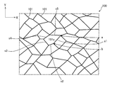
- FIG. 5 is a schematic view illustrating a wiring pattern of the conductive portion 12 and the conductive portion 13 in the touch panel 1.
- the wiring pattern 100 has a random mesh shape.
- the wiring pattern 100 has a plurality of polygonal openings surrounded by the thin metal wires 101.
- the conductive portion 12 of the touch panel 1 and the wiring pattern 100 of the conductive portion 13 are either one of the display panels 2 provided to face each other. It is arranged on the pixel PIX.
- all sides constituting the opening of the wiring pattern 100 are orthogonal to the arrangement direction (X-axis direction) of the sub-pixels 200 of the pixel PIX on the display surface of the display panel 2 (Y-axis direction). ) With an angle satisfying a predetermined condition.
- the Y-axis direction in FIG. 6 indicates the orthogonal direction of the pixel PIX.
- the angle formed with respect to the Y axis is such that the angle formed by the side and the Y axis is greater than ⁇ 1. is doing. That is, in FIG. 6, it is only necessary that the side of the opening is disposed within the range of ⁇ 1. For example, when the end b of the side s1 constituting the opening 101s shown in FIG.
- the side s1 has an ⁇ 1 larger than the angle ⁇ 1 with respect to the Y axis as shown in FIG. Make an angle within the range.
- the other sides s2 to s6 also form an angle in the range of ⁇ 1 that is larger than the angle ⁇ 1 with respect to the Y axis, similarly to the side s1.
- D1 is the sum of binary values excluding the minimum value of the lengths Wr, Wg, and Wb in the X-axis direction of the sub-pixels 200r, 200g, and 200b.
- FIG. 7A when a side sa of an opening forms an angle larger than the angle ⁇ 1 with respect to the Y-axis direction (orthogonal direction), the side sa of the opening is extended.
- the alternate long and short dash line straddles the three RGB sub-pixels 200.
- FIG. 7B when the side sb of an opening has an angle of ⁇ 1 or less with respect to the Y-axis direction (orthogonal direction), the side sb of the opening and one point obtained by extending it A chain line straddles one subpixel 200.
- the side sb of the opening is arranged as shown in FIG.
- FIG. 7B or when the side of the opening is arranged at an angle that straddles only two subpixels 200, illustration is omitted.
- the color balance is lost, causing display glare.
- the side of the opening is arranged at an angle that straddles all three sub-pixels 200, so that it is output to the pixel PIX as compared with the case where only a part of the sub-pixels 200 is arranged.
- the color balance is less likely to be lost, and display glare can be suppressed.
- the length of the side constituting the opening is, for example, 0.05 mm or more and 0.5 mm or less. It is preferable that the sides constituting the opening are arranged so as to cross the three subpixels 200 in one pixel PIX. However, the sides may not necessarily be arranged so as to cross the three subpixels 200. In other words, if the line extending the side constituting the opening forms an angle with respect to the orthogonal direction of the pixel PIX so as to straddle the three subpixels 200 in the pixel PIX, a part of the subpixel PIX It may be arranged across only the pixel 200.
- a mesh-like wiring pattern 100 is formed on the electrode portion 120 a in the conductive portion 12 and the electrode portion 130 a in the conductive portion 13.
- the portions 120b (R) and 130b (R) corresponding to the bridge region R of the connecting portion 130b in the portion 120b and the conductive portion 13 are not formed with the mesh-like wiring pattern 100 like the electrode portion 120a and the electrode portion 130a.
- the connecting portion 120b of the conductive portion 12 of FIG. 8A and the connecting portion 130b of the conductive portion 13 of FIG. 8B are overlapped, as shown in FIG. 8C, a bridge region R where the connecting portion 120b and the connecting portion 130b intersect is formed.
- a random mesh wiring pattern 100 is formed.
- the portion 120b (R) corresponding to the bridge region R of the connecting portion 120b in the conductive portion 12 forms a metal thin wire 101 connected in the X-axis direction as shown in FIG.
- a portion 130b (R) corresponding to the bridge region R of 130b, as shown in FIG. 8B a thin metal wire 101 connected in the Y-axis direction is formed.
- all the sides of the opening of the wiring pattern 100 formed in the conductive portion 12 and the conductive portion 13 are such that a line extending the side straddles the three subpixels 200 in the pixel PIX.
- An angle is formed with respect to the orthogonal direction of the pixel PIX.
- the side of the opening is output to the pixel PIX compared to the case where the side of the opening forms an angle with respect to the orthogonal direction of the pixel PIX so as to straddle some subpixels of the pixel PIX.
- the RGB color balance is less likely to be lost. As a result, a change in display color is reduced, and glare on the display surface is reduced.
- all the sides of the opening of the wiring pattern 100 have the sides of the opening with respect to the orthogonal direction of the pixel PIX so that the extended line straddles all the subpixels of the pixel PIX.
- all the sides of the opening are at an angle with respect to the orthogonal direction of the pixel PIX. It is not necessary to form ⁇ 1. In short, it is only necessary that at least a part of the side of the opening forms an angle ⁇ 1 with respect to the orthogonal direction of the pixel PIX.
- the counter substrate 21 of the display panel 2 includes R, G, B, and Y color filters.
- One pixel in the active matrix substrate 22 includes four subpixels corresponding to any color of the color filter in the counter substrate 21.
- FIG. 9 is a diagram schematically showing one pixel in the present embodiment.
- one pixel PIXa includes R, G, B, and Y sub-pixels 201r, 201g, 201b, and 201y corresponding to each color in the color filter of the counter substrate 21.
- the lengths in the X-axis direction of the R, G, B, and Y subpixels 201r, 201g, 201b, and 201y are Wr, Wg, Wb, and Wy, respectively.
- the length in the X-axis direction of at least one subpixel of the subpixels 201r, 201g, 201b, and 201y is shorter than the length of the other subpixels.
- the width in the Y-axis direction of the subpixels 201r, 201g, 201b, and 201y, that is, the length in the Y-axis direction of the pixel PIXa is L.
- subpixels 201r, 201g, 201b, and 201y are not distinguished, they are referred to as subpixels 201.
- the wiring pattern formed in the conductive part 12 and the conductive part 13 is omitted, like the wiring pattern 100, it is a random mesh-like wiring pattern.
- the sides constituting each opening in the wiring pattern are arranged so as to have an angle satisfying a predetermined condition with respect to the orthogonal direction (Y-axis direction) of the pixel PIXa.
- FIG. 10 is a diagram showing a possible range of an angle formed by the side of the opening of the wiring pattern with respect to the Y-axis direction (orthogonal direction) of the pixel PIX.
- the Y-axis direction in FIG. 10 indicates the orthogonal direction of the pixel PIXa.
- the angle formed by the side and the Y axis is larger than ⁇ 2. As long as it is at an angle. That is, in FIG. 10, it is only necessary that the side of the opening is disposed within the range of ⁇ 2.
- D2 is the sum of three values excluding the minimum value among the lengths Wr, Wg, Wb, and Wy in the X-axis direction of the subpixels 201r, 201g, 201b, and 201y.
- L2 is the length of the pixel PIXa in the Y-axis direction.
- the side sc of an opening when the side sc of an opening has an angle larger than the angle ⁇ 2 with respect to the Y-axis direction (orthogonal direction), the side sc of the opening is extended.
- the alternate long and short dash line straddles the four subpixels 201 of RGBY.
- FIG. 11B and FIG. 11C when the side sd, se of an opening has an angle of ⁇ 2 or less with respect to the Y-axis direction (orthogonal direction), the side sd
- the alternate long and short dash line extends over one subpixel 200r, and the alternate long and short dash line extends over two subpixels 201r and 201g. 11B and FIG.
- the side of the opening is arranged at an angle with respect to the Y-axis direction of the pixel PIXa so as to straddle the four sub-pixels 201, so that the color balance output to the pixel PIXa is balanced. Is less likely to collapse and display glare can be suppressed.
- the side which comprises an opening part is arrange
- the line extending the side forming the opening forms an angle with respect to the orthogonal direction of the pixel PIXa so as to straddle the four subpixels 201 in the pixel PIXa, a part of the subpixel PIXa It may be arranged across only the pixel 201.
- the glare of the display surface is likely to appear when a plurality of pixels arranged in the orthogonal direction of the pixels have the sides of the openings that are substantially parallel to the orthogonal direction. . Therefore, even when the side of the opening crosses only some of the subpixels 201 in one pixel PIXa, the angle formed by the line extending the side of the opening and the orthogonal direction of the pixels PIXa is equal to all the subpixels 201. If the angle crosses the pixel PIXa, even if the color of the pixel PIXa changes depending on the side of the opening, it is suppressed that the pixel PIXa is glaring and visually recognized.
- all the sides of the openings in the wiring patterns formed in the conductive portion 12 and the conductive portion 13 are such that lines extending from the sides straddle the four subpixels 201 of the pixel PIXa.
- An angle is formed with respect to the orthogonal direction of the pixel PIXa.
- the pixel PIXa has an angle with respect to the orthogonal direction of the pixel PIXa so that all the sides of the opening straddle some subpixels of the pixel PIXa.
- the output RGBY color balance is less likely to be lost. As a result, a change in display color is reduced, and glare on the display surface is reduced.
- all the sides of the opening portions of the wiring pattern in the first conductive portion 12 and the second conductive portion 13 are arranged so that the extended line straddles all the subpixels in the pixel PIXa.
- An example in which the angle is larger than the angle ⁇ 2 with respect to the orthogonal direction of PIXa has been described.
- the sides of the opening may not be arranged so that all the sides of the opening have an angle larger than the angle ⁇ 2 with respect to the orthogonal direction. In short, it is only necessary that at least a part of the side of the opening forms an angle ⁇ 2 with respect to the orthogonal direction of the pixel PIXa.
- the touch panel 1 (conductive sheet) of the first embodiment and the second embodiment may be manufactured by a roll-to-roll method.
- a roll-to-roll method an example of the manufacturing process will be described.
- substrate 10 is comprised with the material which has flexibility.
- a metal film is formed on the first main surface 1a of the substrate 10 by sputtering.
- a resist is applied on the metal film formed on the first main surface 1a of the substrate 10 and exposed using a photomask corresponding to the conductive portion 12 on which the wiring pattern 100 is formed.
- the substrate 10 after the second step is etched to remove the resist. Thereby, the electroconductive part 12 is formed in the 1st main surface 1a.
- the first step is performed on the second main surface 1b of the substrate 10, and after applying a resist in the second step, exposure is performed using a photomask corresponding to the conductive portion 13 on which the wiring pattern 100 is formed. To do.
- the third step is performed on the substrate 10 after the second step. Thereby, the conductive portion 13 is formed on the second main surface 1b of the substrate 10.
- the conductive portion (12 or 13) is formed on each side of the substrate 10 (the first main surface 1a or the second main surface 1b), but the first main surface 1a of the substrate 10 and The conductive portion 12 and the conductive portion 13 may be simultaneously formed on the second main surface 1b.
- the sides of the opening of the wiring pattern 100 formed in the conductive portion 12 and the conductive portion 13 are in the above-described orthogonal direction (Y-axis direction) of the pixels PIX and PIXa.
- the angle ⁇ 1 or the angle ⁇ 2 represented by the formula (1) or (2) is set.
- the sides of the openings are the pixels PIX and PIXa so that the lines extending the sides of the openings in the wiring pattern 100 straddle all the subpixels of the pixels PIX and PIXa. The example which made the angle with respect to the orthogonal direction was demonstrated.
- the glare of the display surface due to the side of the opening can be suppressed when the side of the opening is arranged so that the line extending the side of the opening crosses all the subpixels.
- the line extending the side of the opening is arranged at an angle with respect to the orthogonal direction (Y-axis direction) of the pixels PIX and PIXa so as to straddle at least two adjacent subpixels of the pixels PIX and PIXa. If so, glare can be suppressed to some extent. The reason will be described below.
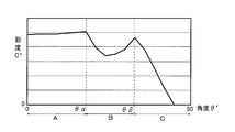
- FIG. 12 is a diagram showing a change in color saturation in a pixel when the side of the opening forms each angle within a range of 0 ° ⁇ ⁇ ⁇ 50 ° with respect to the orthogonal direction of the pixel.
- the angle range A (0 ⁇ ⁇ ⁇ ⁇ ⁇ ) is a range of angles formed by the sides of the opening with respect to the orthogonal direction of the pixel so as to straddle one subpixel in the pixel.
- the angle range B ( ⁇ ⁇ ⁇ ⁇ ) is a range of angles formed by the sides of the opening with respect to the orthogonal direction of the pixel so as to straddle two subpixels in the pixel.
- the angle range C ( ⁇ ⁇ ⁇ 50 °) is a range of angles formed by the sides of the opening with respect to the orthogonal direction of the pixel so as to straddle the three subpixels in the pixel.
- the widths Wr, Wg, Wb in the arrangement direction of the three sub-pixels are all the same, and the color of the metal line is less than a predetermined value.
- the result of simulating the saturation of is shown.
- the width of the side of the opening is set to Wr ⁇ 0.3.
- the saturation C * shown in FIG. 12 is obtained from the intersection of the a * axis and the b * axis when the color in the RGB color space is represented in the chromaticity diagram of the L * a * b * color system.
- This example shows the distance, and in this example, the saturation C * when white (R: 255, G: 255, B: 255) in the RGB color space is displayed on the pixel PIX is shown.
- the saturation C * 0 of the pixel PIX.
- the saturation C * of the pixel is larger than the angle ranges B and C, and is substantially constant.
- the saturation C * of the pixel increases as the angle of the angle range B is approached, but the saturation C * converges to 0 as the angle of the angle range B increases.
- the color balance is lost as compared to the case of straddling three subpixels.
- the saturation C * of the original color can be brought closer than when straddling subpixels, and glare due to the arrangement of the sides of the opening can be reduced.
- a display device with a touch panel may be realized by combining the touch panel 1 with the display panel 2 and a display panel driving unit that drives the display panel 2.
- each pixel in the display panel 2 has three subpixels of RGB or four subpixels of RGBY has been described. It is not limited to subpixels, and may be subpixels of five or more colors.
- the present invention can be industrially used as a display device with a touch panel.
Landscapes
- Engineering & Computer Science (AREA)
- General Engineering & Computer Science (AREA)
- Theoretical Computer Science (AREA)
- Human Computer Interaction (AREA)
- Physics & Mathematics (AREA)
- General Physics & Mathematics (AREA)
- Devices For Indicating Variable Information By Combining Individual Elements (AREA)
Abstract
本発明は、タッチパネルにおけるメッシュ状の金属配線による画素の表示の色味の変化を軽減し、表示面におけるぎらつきを抑制する技術を提供することを目的とする。表示装置は、表示パネルと、表示パネルに対向して設けられたタッチパネルとを備える。表示パネルは、複数の色のサブピクセルを含む画素を有する。タッチパネルは、基板と、基板の第1の主面に設けられた第1導電部と、基板の第2の主面に設けられた第2導電部とを備える。第1導電部と第2導電部の各々は、金属線が多角形状の開口部を形成するように配置されたメッシュ状の金属配線を含む。多角形状の開口部の辺saは、表示パネルの画素PIXにおける直交方向(Y軸方向)に対し、辺saを延長した線が少なくとも隣接する2つのサブピクセルを跨ぐように角度を成して形成されている。
Description
本発明は、タッチパネル付きの表示装置に関する。
近年、スマートフォンやタブレット端末等の様々な装置に、投影型静電容量式タッチパネルが搭載されている。投影型静電容量式タッチパネルは、ドライブラインに複数のドライブ電極が設けられたドライブラインと、複数のセンス電極が設けられたセンスラインとを有する。ドライブラインの複数のドライブ電極を順次駆動し、ドライブ電極とセンス電極の間の静電容量の変化を検出することにより、利用者の指やタッチペンが接触した位置を検出することができる。
投影型静電容量式タッチパネルには、メッシュ状のメタル配線によってドライブ電極とセンス電極とが形成された導電シートを備えるものがある。メッシュ状のメタル配線は透明ではないため、タッチパネルの面内に均一に分布していないと、メタル配線が際立ってしまい、タッチパネルの下に設けられる表示面の視認性を著しく低下させる場合がある。通常、導電シートのメッシュは、一定の角度とピッチを有するパターンの繰り返しによって形成されている。導電シートにおけるメッシュのパターンのピッチと、表示面の画素のピッチとが干渉するとモアレ(干渉縞)の原因となる。そこで、特開2013-093014号公報では、ランダムなメッシュとなるように配線することで、モアレ(干渉縞)の発生を軽減する技術を提案している。
特開2013-093014号公報の技術は、ランダムなメッシュとなるように配線することでモアレの発生を抑制することはできる。しかしながら、メッシュのメタル配線の傾きが、表示面における画素において、特定のサブピクセルに被さるように、サブピクセルの配列方向に対して略直交するような角度となっている場合、その画素における表示の色味が変化し、それがぎらつきとなって視認されることがある。
本発明は、タッチパネルにおけるメッシュ状の金属配線による画素の表示の色味の変化を軽減し、表示面におけるぎらつきを抑制する技術を提供することを目的とする。
第1の発明に係る表示装置は、表示パネルと、前記表示パネルに対向して設けられたタッチパネルとを備える表示装置であって、前記表示パネルは、複数の色の各々に対応する複数のサブピクセルを含む画素を有し、前記タッチパネルは、基板と、前記基板の第1の主面に設けられた第1導電部と、前記基板の第2の主面に設けられた第2導電部と、を備え、前記第1導電部と前記第2導電部の各々は、金属線が多角形状の開口部を形成するように配置されたメッシュ状の金属配線を含み、前記多角形状の開口部の辺は、当該辺を延長した線が、前記表示パネルの画素における前記複数のサブピクセルのうち少なくとも隣接する2つのサブピクセルを跨ぐように、前記複数のサブピクセルの配列方向に直交する直交方向に対して角度を成して形成されている。
第2の発明は、第1の発明において、前記多角形状の開口部の少なくとも一部の辺は、当該辺を延長した線が前記複数のサブピクセルの全てを跨ぐように前記直交方向に対して角度を成して形成されている。
第3の発明は、第1又は第2の発明において、前記直交方向に対して前記多角形状の開口部の辺が成す角度は、以下の式(1)で表される角度θより大きく、
θ=tan-1(D/L) ・・・式(1)
前記式(1)において、前記Dは、前記複数のサブピクセルの前記配列方向の幅のうち最小値の幅を除く他のサブピクセルの前記幅の和であり、前記Lは、前記複数のサブピクセルにおける前記直交方向の幅である。
θ=tan-1(D/L) ・・・式(1)
前記式(1)において、前記Dは、前記複数のサブピクセルの前記配列方向の幅のうち最小値の幅を除く他のサブピクセルの前記幅の和であり、前記Lは、前記複数のサブピクセルにおける前記直交方向の幅である。
第4の発明は、第1から第3のいずれかの発明において、前記複数の色は、R(赤)、G(緑)、及びB(青)である。
第5の発明は、第1から第3のいずれかの発明において、前記複数の色は、R(赤)、G(緑)、B(青)、及びY(黄)である。
本発明の構成によれば、タッチパネルにおけるメッシュ状の金属配線による画素の表示の色味の変化を軽減し、表示面におけるぎらつきを抑制することができる。
本発明の一実施形態に係る表示装置は、表示パネルと、前記表示パネルに対向して設けられたタッチパネルとを備える表示装置であって、前記表示パネルは、複数の色の各々に対応する複数のサブピクセルを含む画素を有し、前記タッチパネルは、基板と、前記基板の第1の主面に設けられた第1導電部と、前記基板の第2の主面に設けられた第2導電部と、を備え、前記第1導電部と前記第2導電部の各々は、金属線が多角形状の開口部を形成するように配置されたメッシュ状の金属配線を含み、前記多角形状の開口部の辺は、当該辺を延長した線が、前記表示パネルの画素における前記複数のサブピクセルのうち少なくとも隣接する2つのサブピクセルを跨ぐように、前記複数のサブピクセルの配列方向に直交する直交方向に対して角度を成して形成されている(第1の構成)。
第1の構成によれば、表示装置は、表示パネルと、表示パネルに対向して設けられたタッチパネルとを備える。表示パネルは、複数の色の各々に対応する複数のサブピクセルを含む画素を有する。タッチパネルは、基板と、基板の第1の主面に設けられた第1導電部と、基板の第2の主面に設けられた第2導電部とを備える。第1導電部と第2導電部は、金属線が多角形状の開口部を形成するように配置されたメッシュ状の金属配線を含む。多角形状の開口部の辺は、その辺を延長した線が、表示パネルの画素における複数のサブピクセルの少なくとも2つのサブピクセルを跨ぐように、サブピクセルの配列方向に直交する直交方向に対して角度を成して形成されている。そのため、1つのサブピクセルだけを跨ぐように開口部の辺が上記直交方向に対して角度を成している場合と比べ、画素における表示の色味の変化を軽減することができ、表示面におけるぎらつきを抑制することができる。
第2の構成は、第1の構成において、前記多角形状の開口部の少なくとも一部の辺は、当該辺を延長した線が前記複数のサブピクセルの全てを跨ぐように前記直交方向に対して角度を成して形成されている、こととしてもよい。
第2の構成によれば、多角形状の開口部の少なくとも一部の辺は、その辺を延長した線が複数のサブピクセルの全てを跨ぐように表示面に配置される。そのため、画素における一部のサブピクセルだけを跨ぐように開口部の辺が上記直交方向に対して角度を成している場合と比べ、画素に出力される色のバランスが崩れにくくなり、表示面におけるぎらつきを抑制することができる。
第3の構成は、第1又は第2の構成において、前記直交方向に対して前記多角形状の開口部の辺が成す角度は、以下の式(1)で表される角度θより大きく、
θ=tan-1(D/L) ・・・式(1)
前記式(1)において、前記Dは、前記複数のサブピクセルにおける前記配列方向の幅のうち最小値の幅を除く他のサブピクセルの前記幅の和であり、前記Lは、前記複数のサブピクセルにおける前記直交方向の幅である、こととしてもよい。
θ=tan-1(D/L) ・・・式(1)
前記式(1)において、前記Dは、前記複数のサブピクセルにおける前記配列方向の幅のうち最小値の幅を除く他のサブピクセルの前記幅の和であり、前記Lは、前記複数のサブピクセルにおける前記直交方向の幅である、こととしてもよい。
第3の構成によれば、多角形状の開口部を構成する辺は、画素の直交方向に対して角度θより大きい角度を成して表示面上に配置されるため、開口部の辺が、画素の上記直交方向に対して角度θ以下の角度を成して配置されている場合と比べ、画素に出力される色のバランスが崩れにくくなり、表示面におけるぎらつきを抑制することができる。
第4の構成は、第1から第3のいずれかの構成において、前記複数の色は、R(赤)、G(緑)、及びB(青)である、こととしてもよい。
第5の構成は、第1から第3のいずれかの構成において、前記複数の色は、R(赤)、G(緑)、B(青)、及びY(黄)である、こととしてもよい。
以下、図面を参照し、本発明の実施の形態を詳しく説明する。図中同一又は相当部分には同一符号を付してその説明は繰り返さない。
<第1実施形態>
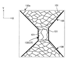
図1は、第1実施形態に係る導電シートの一例であるタッチパネルの概略構成図である。図1は、タッチパネル1の平面図、タッチパネル1をX軸方向に切断したA-A断面図、及びタッチパネル1をY軸方向に切断したB-B断面図を示している。また、図2は、図1に示すタッチパネル1の一部を拡大した平面図である。
図1は、第1実施形態に係る導電シートの一例であるタッチパネルの概略構成図である。図1は、タッチパネル1の平面図、タッチパネル1をX軸方向に切断したA-A断面図、及びタッチパネル1をY軸方向に切断したB-B断面図を示している。また、図2は、図1に示すタッチパネル1の一部を拡大した平面図である。
図1に示すように、タッチパネル1は、基板10と、導電部12及び導電部13とを備える。
基板10は、略矩形状を有し、絶縁性及び透過性を有する材料で構成される。基板10の材料は、例えば、無色透明な樹脂、ガラス、プラスチック、PET(polyethylene terephthalate)等である。
導電部12は、図1のA-A断面図及びB-B断面図に示すように、基板10の第1の主面1aに設けられる。図1に示すように、導電部12は、Y軸方向に配列されたN行(Nは自然数)の導電部12_1~12_Nを有する。本実施形態において、導電部12_1~12_Nの各々は、ドライブ電極としてタッチパネルの駆動回路(図示略)に接続され、駆動回路からの駆動パルスによって順次駆動される。
図2に示すように、導電部12_n(n:自然数、1≦n≦N)は、第1の主面1aのX軸方向に沿って複数設けられた電極部121a,122a,123a…と、隣接する電極部との間を接続する接続部121b,122b…とを有する。以下、これら電極部を区別しないときは、電極部120aと称し、これら接続部を区別しないときは、接続部120bと称する。
一方、導電部13は、図1のA-A断面図及びB-B断面図に示すように、基板10の第2の主面1bに設けられる。図1に示すように、導電部13は、第2の主面1bのX軸方向に配列されたM列(Mは自然数)の導電部13_1~13_Mを有する。本実施形態において、導電部13_1~13_Mの各々は、センス電極としてタッチパネルの検出回路(図示略)に接続される。導電部13_1~13_Mにおいて発生する電流値又は電圧値が検出回路で読み取られ、導電部12_1~12_Nと導電部13_1~13_Mの間の電界の変化が検出される。
図2に示すように、導電部13_m(n;自然数、1≦m≦M)は、第2の主面1bのY軸方向に沿って複数設けられた電極部131a,132a,133a…と、隣接する電極部との間を接続する接続部131b,132b…とを有する。以下、これら電極部を区別しないときは、電極部130aと称し、これら接続部を区別しないときは、接続部130bと称する。
導電部12における電極部120aと接続部120bには、ランダムなメッシュ状の配線パターンが形成されている。また、導電部13における電極部130aと接続部130bには、ランダムなメッシュ状の配線パターンが形成されている。配線パターンの詳細については後述する。
タッチパネル1は、図3に示すように、液晶パネル等の表示パネル2の上に設けられる。表示パネル2は、対向基板21とアクティブマトリクス基板22とを有する。アクティブマトリクス基板22には、ゲート線とソース線とが形成され(いずれも図示略)、ゲート線とソース線とで規定される画素が形成されている。対向基板21は、R(赤)、G(緑)、及びB(青)のカラーフィルタ(図示略)を備え、各々のカラーフィルタは、アクティブマトリクス基板22に形成された画素に対応して設けられる。
図4は、本実施形態における1つの画素を模式的に表した図である。図4に例示するように、1つの画素PIXは、対向基板21のカラーフィルタにおける各色に対応したRGBのサブピクセル200r,200g,200bを含む。この例において、R、G、及びBのサブピクセル200r,200g,200bのX軸方向の長さは、それぞれWr、Wg、Wbである。本実施形態では、サブピクセル200r,200g,200bの少なくとも1つのサブピクセルのX軸方向の長さは、他のサブピクセルのその長さよりも短い。また、サブピクセル200r,200g,200bのY軸方向の幅、つまり、画素PIXのY軸方向の長さはLである。以下、サブピクセル200r,200g,200bを区別しないときは、サブピクセル200と称する。
ここで、本実施形態における配線パターンの具体例について説明する。図5は、タッチパネル1における導電部12及び導電部13の配線パターンを例示した模式図である。図5に例示するように、配線パターン100は、ランダムなメッシュ状を有する。配線パターン100は、金属細線101によって囲まれた多角形状の開口部を複数有する。
図3に示すように、タッチパネル1は、表示パネル2の上に配置されるため、タッチパネル1の導電部12及び導電部13の配線パターン100は、対向して設けられる表示パネル2におけるいずれかの画素PIXの上に配置される。
本実施形態では、配線パターン100の開口部を構成する全ての辺は、表示パネル2の表示面において、画素PIXのサブピクセル200の配列方向(X軸方向)に直交する直交方向(Y軸方向)に対して所定の条件を満たす角度となるように配置されている。
ここで、配線パターン100の各開口部の辺が画素PIXのY軸方向(直交方向)に対して成す角度について図6を用いて説明する。図6におけるY軸方向は、画素PIXの直交方向を示している。本実施形態では、開口部を構成する辺の一端を図6における原点に配置したときに、その辺とY軸とが成す角度がθ1より大きい角度となるようにY軸に対して角度を成している。すなわち、図6において、α1の範囲内に開口部の辺が配置されていればよい。例えば、図5に示す開口部101sを構成する辺s1の端部bを図6の原点に配置すると、図6に示すように、辺s1は、Y軸に対して、角度θ1より大きいα1の範囲内の角度を成している。図示は省略するが、他の辺s2~s6についても辺s1と同様、Y軸に対して角度θ1より大きいα1の範囲内の角度を成している。
角度θ1は、θ1=tan-1(D1/L1)…式(1)で表される。D1は、サブピクセル200r,200g,200bのX軸方向の長さWr、Wg、Wbのうち最小値を除く2値の和である。L1は、画素PIXのY軸方向の長さである。例えば、サブピクセル200r,200g,200bのX軸方向の長さWr、Wg、Wbのうち、サブピクセル200bの長さWbが最小値である場合、角度θ1は、θ1=tan-1((Wr+Wg)/L)で表される。
つまり、図7Aに例示するように、ある開口部の辺saがY軸方向(直交方向)に対して角度θ1より大きい角度を成している場合には、開口部の辺saとそれを延長した一点鎖線はRGBの3つのサブピクセル200を跨ぐ。一方、図7Bに例示すように、ある開口部の辺sbがY軸方向(直交方向)に対して角度θ1以下の角度を成している場合、開口部の辺sbとそれを延長した一点鎖線は1つのサブピクセル200を跨ぐ。図7Bのように開口部の辺sbが配置される場合や、図示を省略するが、2つのサブピクセル200だけを跨ぐような角度で開口部の辺が配置される場合、画素PIXに出力される色のバランスが崩れ、表示のぎらつきの原因となる。図7Aのように、3つの全てのサブピクセル200を跨ぐような角度で開口部の辺が配置されることで、一部のサブピクセル200だけに配置される場合と比べ、画素PIXに出力される色のバランスが崩れにくくなり、表示のぎらつきを抑制することができる。
開口部を構成する辺の長さは、例えば、0.05mm以上、0.5mm以下である。開口部を構成する辺が1つの画素PIXにおける3つのサブピクセル200を横切るように配置されることが好ましいが、必ずしも、3つのサブピクセル200を横切るように配置されていなくてもよい。すなわち、開口部を構成する辺を延長した線が、画素PIXにおける3つのサブピクセル200を跨ぐように、画素PIXの直交方向に対して角度を成していれば、画素PIXの一部のサブピクセル200だけを横切って配置されてもよい。
開口部の辺によって色が変化した複数の画素が縦長に連なっている場合、それが、画素の直交方向にぎらつきとなって視認される。つまり、表示面のぎらつきは、画素の直交方向に配列された複数の画素において、その直交方向に略平行な開口部の辺が配置される場合に現れやすい。そのため、開口部の辺が1つの画素PIXにおける1又は2つのサブピクセル200しか横切っていない場合でも、開口部の辺を延長した線と画素PIXの直交方向とがなす角度が3つのサブピクセル200を跨ぐ角度であれば、開口部の辺によって画素PIXの色は変化しても、それがぎらつきとなって視認されることは抑制される。
本実施形態では、図8A及び図8Bに示すように、導電部12における電極部120aと導電部13における電極部130aには、メッシュ状の配線パターン100が形成されるが、導電部12における接続部120bと導電部13における接続部130bのブリッジ領域Rに対応する部分120b(R),130b(R)は、電極部120aと電極部130aのようなメッシュ状の配線パターン100が形成されていない。図8Aの導電部12の接続部120bと図8Bの導電部13の接続部130bとを重ね合せると、図8Cに示すように、接続部120bと接続部130bとが交差するブリッジ領域Rに、ランダムなメッシュ状の配線パターン100が形成されるようになっている。接続部120bと接続部130bに、電極部120aと電極部130aと同様のメッシュ状の配線パターン100を形成する場合、ブリッジ領域Rにおける接続部120bと接続部130bの配線パターン100のメッシュの位置を合せることが困難である。そのため、導電部12における接続部120bのブリッジ領域Rに対応する部分120b(R)は、図8Aに示すように、X軸方向に接続された金属細線101を形成し、導電部13における接続部130bのブリッジ領域Rに対応する部分130b(R)には、図8Bに示すように、Y軸方向に接続された金属細線101を形成している。
上述した第1実施形態では、導電部12及び導電部13に形成されている配線パターン100の開口部の全ての辺は、辺を延長した線が画素PIXにおける3つのサブピクセル200を跨ぐように画素PIXの直交方向に対して角度を成している。このように構成することにより、開口部の辺が、画素PIXの一部のサブピクセルを跨ぐように画素PIXの直交方向に対して角度を成している場合と比べ、画素PIXに出力されるRGBの色のバランスが崩れにくくなる。その結果、表示の色味の変化が軽減され、表示面のぎらつきが軽減される。
なお、上記第1実施形態では、配線パターン100の開口部の全ての辺は、その延長した線が画素PIXの全てのサブピクセルを跨ぐように、開口部の辺が画素PIXの直交方向に対して角度θ1より大きい角度を成して配置されている例を説明したが、表示面のぎらつきを許容可能な範囲であれば、開口部の全ての辺が画素PIXの直交方向に対して角度θ1を成していなくてもよい。要は、開口部の少なくとも一部の辺が画素PIXの直交方向に対して角度θ1を成していればよい。
<第2実施形態>
上述した第1実施形態では、表示パネル2における画素がRGBの3つのサブピクセル200を含む場合の例を説明したが、本実施形態では、1つの画素がR、G、B、及びY(黄)の4つのサブピクセルを含む場合ついて説明する。
上述した第1実施形態では、表示パネル2における画素がRGBの3つのサブピクセル200を含む場合の例を説明したが、本実施形態では、1つの画素がR、G、B、及びY(黄)の4つのサブピクセルを含む場合ついて説明する。
本実施形態では、表示パネル2の対向基板21は、R、G、B、及びYのカラーフィルタを備える。アクティブマトリクス基板22における1つの画素は、対向基板21におけるカラーフィルタのいずれかの色に対応する4つのサブピクセルを含む。
図9は、本実施形態における1つの画素を模式的に表した図である。図9に例示するように、1つの画素PIXaは、対向基板21のカラーフィルタにおける各色に対応したR、G、B、及びYのサブピクセル201r,201g,201b,201yを含む。この例において、R、G、B、及びYのサブピクセル201r,201g,201b,201yのX軸方向の長さは、それぞれWr、Wg、Wb、Wyである。本実施形態では、サブピクセル201r,201g,201b,201yの少なくとも1つのサブピクセルのX軸方向の長さは、他のサブピクセルのその長さよりも短い。また、サブピクセル201r,201g,201b,201yのY軸方向の幅、つまり、画素PIXaのY軸方向の長さはLである。以下、サブピクセル201r,201g,201b,201yを区別しないときは、サブピクセル201と称する。
本実施形態では、導電部12及び導電部13に形成される配線パターンの図示を省略するが、上記配線パターン100と同様、ランダムなメッシュ状の配線パターンである。配線パターンにおける各開口部を構成する辺は、画素PIXaの直交方向(Y軸方向)に対して所定の条件を満たす角度となるように配置されている。
図10は、配線パターンの開口部の辺が画素PIXのY軸方向(直交方向)に対して成す角度の取り得る範囲を示す図である。図10におけるY軸方向は、画素PIXaの直交方向を示している。上記第1実施形態と同様、開口部の全ての辺が、図10における原点に辺の一端を配置したときに、その辺とY軸とが成す角度がθ2より大きい角度となるようにY軸に対して角度を成していればよい。すなわち、図10において、α2の範囲内に開口部の辺が配置されていればよい。
なお、角度θ2は、θ2=tan-1(D2/L2)…式(2)で表される。D2は、サブピクセル201r,201g,201b,201yのX軸方向の長さWr、Wg、Wb、Wyのうち最小値を除く3値の和である。L2は、画素PIXaのY軸方向の長さである。例えば、サブピクセル201r,201g,201b,201yのX軸方向の長さWr、Wg、Wb、Wyのうち、サブピクセル200yの長さWyが最小値である場合、角度θ2は、θ2=tan-1((Wr+Wg+Wb)/L)で表される。
つまり、図11Aに例示するように、ある開口部の辺scがY軸方向(直交方向)に対して角度θ2より大きい角度を成している場合には、開口部の辺scとそれを延長した一点鎖線はRGBYの4つのサブピクセル201を跨ぐ。一方、例えば、図11B、図11Cに例示するように、ある開口部の辺sd、seがY軸方向(直交方向)に対して角度θ2以下の角度を成している場合には、辺sdを延長した一点鎖線は1つのサブピクセル200rを跨ぎ、辺seを延長した一点鎖線は2つのサブピクセル201r,201gを跨ぐ。図11B、図11Cのように開口部の辺を延長した線が1つ又は2つのサブピクセル201を跨ぐ場合、また、図示を省略するが、3つのサブピクセル201だけを跨ぐような場合、画素PIXaに出力される色のバランスが崩れ、表示のぎらつきの原因となる。図11Aのように、4つのサブピクセル201を跨ぐように、開口部の辺が画素PIXaのY軸方向に対して角度を成して配置されることにより、画素PIXaに出力される色のバランスが崩れにくくなり、表示のぎらつきを抑制することができる。
なお、開口部を構成する辺が1つの画素PIXaの全てのサブピクセル201を横切るように配置されることが好ましいが、必ずしも、全てのサブピクセル201を横切るように配置されていなくてもよい。すなわち、開口部を構成する辺を延長した線が、画素PIXaにおける4つのサブピクセル201を跨ぐように、画素PIXaの直交方向に対して角度を成していれば、画素PIXaの一部のサブピクセル201だけを横切って配置されてもよい。
上記第1実施形態でも述べたように、表示面のぎらつきは、画素の直交方向に配列された複数の画素において、その直交方向に略平行な開口部の辺が配置される場合に現れやすい。そのため、開口部の辺が1つの画素PIXaにおける一部のサブピクセル201しか横切っていない場合でも、開口部の辺を延長した線と画素PIXaの直交方向とがなす角度が、全てのサブピクセル201を跨ぐ角度であれば、開口部の辺によって画素PIXaの色は変化しても、それがぎらつきとなって視認されることは抑制される。
上述した第2実施形態では、導電部12及び導電部13に形成されている配線パターンにおける開口部の全ての辺は、辺を延長した線が画素PIXaの4つのサブピクセル201を跨ぐように、画素PIXaの直交方向に対して角度を成している。このように構成することにより、開口部の全ての辺が、画素PIXaの一部のサブピクセルを跨ぐように、画素PIXaの直交方向に対して角度を成している場合と比べ、画素PIXaに出力されるRGBYの色のバランスが崩れにくくなる。その結果、表示の色味の変化が軽減され、表示面のぎらつきが軽減される。
なお、上記第2実施形態では、第1導電部12及び第2導電部13における配線パターンの開口部の全ての辺が、その延長した線が画素PIXaにおける全てのサブピクセルを跨ぐように、画素PIXaの直交方向に対して角度θ2より大きい角度を成して配置されている例を説明した。しかしながら、表示面のぎらつきを許容可能な範囲であれば、開口部の全ての辺が直交方向に対し、角度θ2より大きい角度となるように開口部の辺が配置されていなくてもよい。要は、開口部の少なくとも一部の辺が画素PIXaの直交方向に対して角度θ2を成していればよい。
<導電シートの製造方法>
第1実施形態及び第2実施形態のタッチパネル1(導電シート)を、ロールツーロール(roll-to-roll)方式で製造してもよい。以下、その製造工程の一例について説明する。なお、ロールツーロール方式で製造する場合、基板10は、可撓性を有する材料で構成される。
第1実施形態及び第2実施形態のタッチパネル1(導電シート)を、ロールツーロール(roll-to-roll)方式で製造してもよい。以下、その製造工程の一例について説明する。なお、ロールツーロール方式で製造する場合、基板10は、可撓性を有する材料で構成される。
まず、第1工程において、基板10の第1の主面1aに、スパッタリングにより金属膜を成膜する。
第2工程において、基板10の第1の主面1aに形成された金属膜の上にレジストを塗布し、配線パターン100が形成された導電部12に対応するフォトマスクを用いて露光する。
第3工程において、第2工程後の基板10をエッチングし、レジストを除去する。これにより、第1の主面1aに導電部12が形成される。
同様にして、基板10の第2の主面1bにおいて上記第1工程を行い、上記第2工程においてレジストを塗布後、配線パターン100が形成された導電部13に対応するフォトマスクを用いて露光する。そして、第2工程後の基板10に対して上記第3工程を行う。これにより、基板10の第2の主面1bに導電部13が形成される。
上記した製造方法の例では、基板10の片面(第1の主面1a又は第2の主面1b)ずつ導電部(12又は13)を形成したが、基板10の第1の主面1aと第2の主面1bに導電部12と導電部13を各々同時に形成してもよい。
以上、本発明の実施の形態を説明したが、上述した実施の形態は本発明を実施するための例示に過ぎない。よって、本発明は上述した実施の形態に限定されることなく、その趣旨を逸脱しない範囲内で上述した実施の形態を適宜変形して実施することが可能である。以下、本発明の変形例について説明する。
<変形例1>
上述した第1実施形態及び第2実施形態では、画素PIX、PIXaにおけるサブピクセルのうち、少なくとも1つのサブピクセルのX軸方向の長さは他のサブピクセルのその長さより短い場合について説明したが、各サブピクセルのX軸方向の幅が略同等の長さであってもよい。この場合には、上記式(1)と式(2)におけるD1とD2は、いずれか1つのサブピクセルを除く他のサブピクセルのX軸方向の長さの和とすればよい。
上述した第1実施形態及び第2実施形態では、画素PIX、PIXaにおけるサブピクセルのうち、少なくとも1つのサブピクセルのX軸方向の長さは他のサブピクセルのその長さより短い場合について説明したが、各サブピクセルのX軸方向の幅が略同等の長さであってもよい。この場合には、上記式(1)と式(2)におけるD1とD2は、いずれか1つのサブピクセルを除く他のサブピクセルのX軸方向の長さの和とすればよい。
<変形例2>
上述した第1実施形態及び第2実施形態では、導電部12及び導電部13に形成される配線パターン100の開口部の辺が、画素PIX、PIXaの直交方向(Y軸方向)に対し、上記式(1)又は(2)で表される角度θ1又はθ2より大きい角度を成して配置されている例であった。すなわち、第1実施形態及び第2実施形態では配線パターン100における開口部の辺を延長した線が、画素PIX,PIXaの全てのサブピクセルを跨ぐように、開口部の辺が画素PIX,PIXaの直交方向に対して角度を成している例を説明した。
上述した第1実施形態及び第2実施形態では、導電部12及び導電部13に形成される配線パターン100の開口部の辺が、画素PIX、PIXaの直交方向(Y軸方向)に対し、上記式(1)又は(2)で表される角度θ1又はθ2より大きい角度を成して配置されている例であった。すなわち、第1実施形態及び第2実施形態では配線パターン100における開口部の辺を延長した線が、画素PIX,PIXaの全てのサブピクセルを跨ぐように、開口部の辺が画素PIX,PIXaの直交方向に対して角度を成している例を説明した。
開口部の辺を延長した線が全てのサブピクセルを跨ぐように開口部の辺が配置されている方が、開口部の辺による表示面のぎらつきを抑制することができる。しかしながら、開口部の辺を延長した線が、画素PIX,PIXaの少なくとも隣接する2つのサブピクセルを跨ぐように、画素PIX,PIXaにおける直交方向(Y軸方向)に対し角度を成して配置されていれば、ある程度ぎらつきを抑制することができる。以下、その理由について説明する。
図12は、開口部の辺が、画素の直交方向に対し、0°≦θ≦50°の範囲内の各々の角度を成す場合の画素における色の彩度の変化を表す図である。図12において、角度範囲A(0≦θ≦θα)は、画素における1つのサブピクセルを跨ぐように、画素の直交方向に対して開口部の辺が成す角度の範囲である。角度範囲B(θα<θ≦θβ)は、画素における2つのサブピクセルを跨ぐように、画素の直交方向に対して開口部の辺が成す角度の範囲である。角度範囲C(θβ<θ≦50°)は、画素における3つのサブピクセルを跨ぐように、画素の直交方向に対して開口部の辺が成す角度の範囲である。
また、図12では、図4に示した画素PIXにおいて、3つのサブピクセルの配列方向の幅Wr,Wg,Wbが全て同じであり、金属線の幅が所定値以下となる条件下で、色の彩度をシミュレーションした結果を示している。この例では、開口部の辺の幅は、Wr×0.3に設定されている。また、図12に示す彩度C*は、RGBの色空間における色を、L*a*b*表色系の色度図に表したときの、a*軸とb*軸の交点からの距離を示しており、この例では、画素PIXにRGBの色空間における白色(R:255,G:255,B:255)を表示した場合の彩度C*を表している。
画素PIXに金属細線が配置されていない場合、画素PIXの彩度C*=0である。図12に示すように、角度範囲Aでは、角度範囲B、Cよりも画素の彩度C*は大きくなり、略一定している。また、角度範囲Bでは、画素の彩度C*は元の白色の彩度C*(=0)に収束しないが、角度範囲Aよりも彩度C*の値は小さくなっている。角度範囲Cでは、角度範囲Bの角度に近づくほど、画素の彩度C*は大きくなるが、角度範囲Bの角度より大きくなるほど彩度C*は0に収束する。
つまり、開口部の辺が2つのサブピクセルを跨ぐように画素PIXの直交方向に対して角度を成している場合、3つのサブピクセルを跨ぐ場合と比べて色のバランスは崩れるが、1つのサブピクセルを跨ぐ場合よりも元の色の彩度C*に近づけることができ、開口部の辺の配置によるぎらつきを軽減することができる。
<変形例3>
上述した第1実施形態及び第2実施形態において、タッチパネル1に、表示パネル2及び表示パネル2を駆動する表示パネル駆動部を組み合わせ、タッチパネル付き表示装置を実現してもよい。
上述した第1実施形態及び第2実施形態において、タッチパネル1に、表示パネル2及び表示パネル2を駆動する表示パネル駆動部を組み合わせ、タッチパネル付き表示装置を実現してもよい。
<変形例4>
上述したタッチパネルの製造方法の工程の実行順序は、上記記載の順序に限定されるものではなく、発明の要旨を逸脱しない範囲で適宜実行順序を入れ替えてもよい。
上述したタッチパネルの製造方法の工程の実行順序は、上記記載の順序に限定されるものではなく、発明の要旨を逸脱しない範囲で適宜実行順序を入れ替えてもよい。
<変形例5>
上述した第1実施形態及び第2実施形態では、表示パネル2における各画素が、RGBの3色のサブピクセル又はRGBYの4色のサブピクセルを有する例を説明したが、3色又は4色のサブピクセルに限らず、5色以上のサブピクセルであってもよい。
上述した第1実施形態及び第2実施形態では、表示パネル2における各画素が、RGBの3色のサブピクセル又はRGBYの4色のサブピクセルを有する例を説明したが、3色又は4色のサブピクセルに限らず、5色以上のサブピクセルであってもよい。
<変形例6>
上述した実施形態及び変形例2では、開口部の辺を延長した線が少なくとも2つのサブピクセルを跨ぐように画素の直交方向に対して角度を成している例、つまり、開口部の辺が画素の直交方向に対して非平行である場合について説明したが、開口部の辺が画素の直交方向に対して略平行である場合には、開口部の辺の長さを規定することにより表示面のぎらつきを抑制してもよい。この場合には、例えば、画素の直交方向に対して略平行な金属線(開口部の辺)の長さを変えて画素に配置したときの画素の色の変化をシミュレーションした結果に基づき、ぎらつきの許容範囲内で開口部の辺の長さを規定してもよい。
上述した実施形態及び変形例2では、開口部の辺を延長した線が少なくとも2つのサブピクセルを跨ぐように画素の直交方向に対して角度を成している例、つまり、開口部の辺が画素の直交方向に対して非平行である場合について説明したが、開口部の辺が画素の直交方向に対して略平行である場合には、開口部の辺の長さを規定することにより表示面のぎらつきを抑制してもよい。この場合には、例えば、画素の直交方向に対して略平行な金属線(開口部の辺)の長さを変えて画素に配置したときの画素の色の変化をシミュレーションした結果に基づき、ぎらつきの許容範囲内で開口部の辺の長さを規定してもよい。
本発明は、タッチパネル付き表示装置として産業上の利用が可能である。
Claims (5)
- 表示パネルと、前記表示パネルに対向して設けられたタッチパネルとを備える表示装置であって、
前記表示パネルは、
複数の色の各々に対応する複数のサブピクセルを含む画素を有し、
前記タッチパネルは、
基板と、
前記基板の第1の主面に設けられた第1導電部と、
前記基板の第2の主面に設けられた第2導電部と、を備え、
前記第1導電部と前記第2導電部の各々は、金属線が多角形状の開口部を形成するように配置されたメッシュ状の金属配線を含み、
前記多角形状の開口部の辺は、当該辺を延長した線が、前記表示パネルの画素における前記複数のサブピクセルのうち少なくとも隣接する2つのサブピクセルを跨ぐように、前記複数のサブピクセルの配列方向に直交する直交方向に対して角度を成して形成されている、表示装置。 - 前記多角形状の開口部の少なくとも一部の辺は、当該辺を延長した線が前記複数のサブピクセルの全てを跨ぐように前記直交方向に対して角度を成して形成されている、請求項1に記載の表示装置。
- 前記直交方向に対して前記多角形状の開口部の辺が成す角度は、以下の式(1)で表される角度θより大きく、
θ=tan-1(D/L) ・・・式(1)
前記式(1)において、前記Dは、前記複数のサブピクセルの前記配列方向の幅のうち最小値の幅を除く他のサブピクセルの前記幅の和であり、前記Lは、前記複数のサブピクセルにおける前記直交方向の幅である、請求項1又は2に記載の表示装置。 - 前記複数の色は、R(赤)、G(緑)、及びB(青)である、請求項1から3のいずれか一項に記載の表示装置。
- 前記複数の色は、R(赤)、G(緑)、B(青)、及びY(黄)である、請求項1から3のいずれか一項に記載の表示装置。
Applications Claiming Priority (2)
| Application Number | Priority Date | Filing Date | Title |
|---|---|---|---|
| JP2013258338 | 2013-12-13 | ||
| JP2013-258338 | 2013-12-13 |
Publications (1)
| Publication Number | Publication Date |
|---|---|
| WO2015087863A1 true WO2015087863A1 (ja) | 2015-06-18 |
Family
ID=53371165
Family Applications (1)
| Application Number | Title | Priority Date | Filing Date |
|---|---|---|---|
| PCT/JP2014/082518 Ceased WO2015087863A1 (ja) | 2013-12-13 | 2014-12-09 | 表示装置 |
Country Status (1)
| Country | Link |
|---|---|
| WO (1) | WO2015087863A1 (ja) |
Cited By (1)
| Publication number | Priority date | Publication date | Assignee | Title |
|---|---|---|---|---|
| WO2017065085A1 (ja) * | 2015-10-16 | 2017-04-20 | 富士フイルム株式会社 | 導電性フィルム、及びこれを備える表示装置 |
Citations (2)
| Publication number | Priority date | Publication date | Assignee | Title |
|---|---|---|---|---|
| JP2013020785A (ja) * | 2011-07-11 | 2013-01-31 | Fujifilm Corp | 導電性積層体、タッチパネル及び表示装置 |
| JP2013037682A (ja) * | 2011-07-11 | 2013-02-21 | Fujifilm Corp | 導電シート、タッチパネル及び表示装置 |
-
2014
- 2014-12-09 WO PCT/JP2014/082518 patent/WO2015087863A1/ja not_active Ceased
Patent Citations (2)
| Publication number | Priority date | Publication date | Assignee | Title |
|---|---|---|---|---|
| JP2013020785A (ja) * | 2011-07-11 | 2013-01-31 | Fujifilm Corp | 導電性積層体、タッチパネル及び表示装置 |
| JP2013037682A (ja) * | 2011-07-11 | 2013-02-21 | Fujifilm Corp | 導電シート、タッチパネル及び表示装置 |
Cited By (3)
| Publication number | Priority date | Publication date | Assignee | Title |
|---|---|---|---|---|
| WO2017065085A1 (ja) * | 2015-10-16 | 2017-04-20 | 富士フイルム株式会社 | 導電性フィルム、及びこれを備える表示装置 |
| JP2017076336A (ja) * | 2015-10-16 | 2017-04-20 | 富士フイルム株式会社 | 導電性フィルム、及びこれを備える表示装置 |
| US10359896B2 (en) | 2015-10-16 | 2019-07-23 | Fujifilm Corporation | Conductive film and display device including the same |
Similar Documents
| Publication | Publication Date | Title |
|---|---|---|
| JP5900818B2 (ja) | 液晶表示装置 | |
| JP6266263B2 (ja) | タッチパネル及びタッチパネルを備えた液晶表示装置 | |
| US9626027B2 (en) | Touch sensor integrated type display device | |
| CN104009064B (zh) | 彩色显示面板的像素配置 | |
| US10521059B2 (en) | Touch panel, mutual capacitive touch screen, and touch display device | |
| CN105094409B (zh) | 触控显示面板 | |
| CN104360773B (zh) | 一种触控显示装置及电子设备 | |
| CN105845033A (zh) | 一种显示面板、其制作方法及显示装置 | |
| JP2014531640A (ja) | カラーフィルター基板とコンデンサ式タッチスクリーン | |
| WO2015045603A1 (ja) | 導電シート、タッチパネル装置、表示装置、および、導電シート製造方法 | |
| KR101527320B1 (ko) | 매트릭스 스위칭 타입 터치패널 | |
| JP2019028095A (ja) | 表示装置 | |
| CN105988613A (zh) | 触控感应电极层及显示装置 | |
| KR20160034020A (ko) | 터치 센서 패널 및 그의 제조 방법 | |
| CN106133657A (zh) | 带触摸面板的显示装置 | |
| JP2015132709A (ja) | 表示装置 | |
| CN107562249A (zh) | 触控显示装置 | |
| CN109683386B (zh) | 内嵌触控液晶显示器 | |
| CN104090415A (zh) | 彩膜基板及显示装置 | |
| JP6400935B2 (ja) | 表示装置 | |
| WO2015087863A1 (ja) | 表示装置 | |
| CN112116874B (zh) | 显示面板及显示装置 | |
| JP2015206829A (ja) | 表示装置 | |
| EP3688565B1 (en) | Touch control module and fabricating method thereof and touch control display apparatus | |
| CN115798336B (zh) | 显示面板和显示装置 |
Legal Events
| Date | Code | Title | Description |
|---|---|---|---|
| 121 | Ep: the epo has been informed by wipo that ep was designated in this application |
Ref document number: 14869849 Country of ref document: EP Kind code of ref document: A1 |
|
| NENP | Non-entry into the national phase |
Ref country code: DE |
|
| 122 | Ep: pct application non-entry in european phase |
Ref document number: 14869849 Country of ref document: EP Kind code of ref document: A1 |
|
| NENP | Non-entry into the national phase |
Ref country code: JP |