WO2015068599A1 - 光拡散部材、光拡散部材の検査装置、光拡散部材の製造装置及び製造方法 - Google Patents
光拡散部材、光拡散部材の検査装置、光拡散部材の製造装置及び製造方法 Download PDFInfo
- Publication number
- WO2015068599A1 WO2015068599A1 PCT/JP2014/078377 JP2014078377W WO2015068599A1 WO 2015068599 A1 WO2015068599 A1 WO 2015068599A1 JP 2014078377 W JP2014078377 W JP 2014078377W WO 2015068599 A1 WO2015068599 A1 WO 2015068599A1
- Authority
- WO
- WIPO (PCT)
- Prior art keywords
- light
- diffusing member
- light diffusing
- base material
- face
- Prior art date
- Legal status (The legal status is an assumption and is not a legal conclusion. Google has not performed a legal analysis and makes no representation as to the accuracy of the status listed.)
- Ceased
Links
Images











Classifications
-
- G—PHYSICS
- G02—OPTICS
- G02B—OPTICAL ELEMENTS, SYSTEMS OR APPARATUS
- G02B5/00—Optical elements other than lenses
- G02B5/02—Diffusing elements; Afocal elements
- G02B5/0273—Diffusing elements; Afocal elements characterized by the use
- G02B5/0278—Diffusing elements; Afocal elements characterized by the use used in transmission
-
- G—PHYSICS
- G02—OPTICS
- G02B—OPTICAL ELEMENTS, SYSTEMS OR APPARATUS
- G02B5/00—Optical elements other than lenses
- G02B5/02—Diffusing elements; Afocal elements
- G02B5/0205—Diffusing elements; Afocal elements characterised by the diffusing properties
- G02B5/0236—Diffusing elements; Afocal elements characterised by the diffusing properties the diffusion taking place within the volume of the element
-
- G—PHYSICS
- G02—OPTICS
- G02F—OPTICAL DEVICES OR ARRANGEMENTS FOR THE CONTROL OF LIGHT BY MODIFICATION OF THE OPTICAL PROPERTIES OF THE MEDIA OF THE ELEMENTS INVOLVED THEREIN; NON-LINEAR OPTICS; FREQUENCY-CHANGING OF LIGHT; OPTICAL LOGIC ELEMENTS; OPTICAL ANALOGUE/DIGITAL CONVERTERS
- G02F1/00—Devices or arrangements for the control of the intensity, colour, phase, polarisation or direction of light arriving from an independent light source, e.g. switching, gating or modulating; Non-linear optics
- G02F1/01—Devices or arrangements for the control of the intensity, colour, phase, polarisation or direction of light arriving from an independent light source, e.g. switching, gating or modulating; Non-linear optics for the control of the intensity, phase, polarisation or colour
- G02F1/13—Devices or arrangements for the control of the intensity, colour, phase, polarisation or direction of light arriving from an independent light source, e.g. switching, gating or modulating; Non-linear optics for the control of the intensity, phase, polarisation or colour based on liquid crystals, e.g. single liquid crystal display cells
- G02F1/1303—Apparatus specially adapted to the manufacture of LCDs
-
- G—PHYSICS
- G02—OPTICS
- G02F—OPTICAL DEVICES OR ARRANGEMENTS FOR THE CONTROL OF LIGHT BY MODIFICATION OF THE OPTICAL PROPERTIES OF THE MEDIA OF THE ELEMENTS INVOLVED THEREIN; NON-LINEAR OPTICS; FREQUENCY-CHANGING OF LIGHT; OPTICAL LOGIC ELEMENTS; OPTICAL ANALOGUE/DIGITAL CONVERTERS
- G02F1/00—Devices or arrangements for the control of the intensity, colour, phase, polarisation or direction of light arriving from an independent light source, e.g. switching, gating or modulating; Non-linear optics
- G02F1/01—Devices or arrangements for the control of the intensity, colour, phase, polarisation or direction of light arriving from an independent light source, e.g. switching, gating or modulating; Non-linear optics for the control of the intensity, phase, polarisation or colour
- G02F1/13—Devices or arrangements for the control of the intensity, colour, phase, polarisation or direction of light arriving from an independent light source, e.g. switching, gating or modulating; Non-linear optics for the control of the intensity, phase, polarisation or colour based on liquid crystals, e.g. single liquid crystal display cells
- G02F1/1306—Details
- G02F1/1309—Repairing; Testing
-
- G—PHYSICS
- G02—OPTICS
- G02F—OPTICAL DEVICES OR ARRANGEMENTS FOR THE CONTROL OF LIGHT BY MODIFICATION OF THE OPTICAL PROPERTIES OF THE MEDIA OF THE ELEMENTS INVOLVED THEREIN; NON-LINEAR OPTICS; FREQUENCY-CHANGING OF LIGHT; OPTICAL LOGIC ELEMENTS; OPTICAL ANALOGUE/DIGITAL CONVERTERS
- G02F1/00—Devices or arrangements for the control of the intensity, colour, phase, polarisation or direction of light arriving from an independent light source, e.g. switching, gating or modulating; Non-linear optics
- G02F1/01—Devices or arrangements for the control of the intensity, colour, phase, polarisation or direction of light arriving from an independent light source, e.g. switching, gating or modulating; Non-linear optics for the control of the intensity, phase, polarisation or colour
- G02F1/13—Devices or arrangements for the control of the intensity, colour, phase, polarisation or direction of light arriving from an independent light source, e.g. switching, gating or modulating; Non-linear optics for the control of the intensity, phase, polarisation or colour based on liquid crystals, e.g. single liquid crystal display cells
- G02F1/133—Constructional arrangements; Operation of liquid crystal cells; Circuit arrangements
- G02F1/1333—Constructional arrangements; Manufacturing methods
- G02F1/1335—Structural association of cells with optical devices, e.g. polarisers or reflectors
- G02F1/133504—Diffusing, scattering, diffracting elements
Definitions
- the present invention relates to a light diffusing member, a light diffusing member inspection apparatus, and a light diffusing member manufacturing apparatus and method.
- This application claims priority based on Japanese Patent Application No. 2013-229669 filed in Japan on November 5, 2013, the contents of which are incorporated herein by reference.
- Liquid crystal display devices are widely used as displays for portable electronic devices such as mobile phones, televisions, personal computers, and the like.
- the liquid crystal display device is generally excellent in visibility from the front side, but generally has a characteristic that a viewing angle is narrow. For this reason, in the liquid crystal display device, various devices for widening the viewing angle have been conventionally performed.
- a light diffusing member is arranged on the viewing side of the liquid crystal panel (display body), and light emitted from the viewing side of the liquid crystal panel is diffused using the light diffusing member. .
- a transparent base material, a light diffusing portion having a tapered side surface formed on one surface of the transparent base material, and a light diffusing member forming region on one surface of the transparent base material are formed in a region other than the region.
- a light diffusing member including the light shielding layer is disclosed.
- ultraviolet light UV light
- a transparent negative resist is patterned and the light-diffusion part which has the taper-shaped side surface mentioned above is formed.
- the light diffusion characteristics of the light diffusion member are greatly affected by the quality of the light diffusion portion. That is, in order to obtain a desired light diffusion characteristic, it is important that the shape and dimensions of the light diffusion portion are finished as originally designed.
- the light diffusing member has a desired light diffusing characteristic
- a method of confirming the display characteristic after actually bonding the light diffusing member to the viewing side of the liquid crystal panel must be used. Therefore, the light diffusion characteristics of the light diffusing member continuously produced by the roll-to-roll (RtoR) method could not be in-line tested.
- the light diffusing member can be easily and accurately inspected for the light diffusing member and can be used for in-line inspection. Another object is to provide a light diffusing member inspection apparatus, and a light diffusing member manufacturing apparatus and method using such an inspection apparatus.
- a light diffusing member includes a light-transmitting base material, a light diffusing portion formed at a predetermined height on one surface of the base material, and one surface of the base material.
- a light-shielding layer formed in a region other than the light diffusion portion with a thickness smaller than the height of the light diffusion portion, the light diffusion portion contacting the base material, and the light
- a light diffusing member that includes a light incident end surface that faces the light emitting end surface and has an area larger than the area of the light emitting end surface, and information is recorded in the member.
- the information may be defect information.
- the information may be information on the position and type of a defective portion.
- the recording position may be close to the position of the defective portion.
- the recording position may be in an area where a light diffusing portion is not provided in the substrate.
- the light diffusing member inspection apparatus includes a light-transmitting base material, a light diffusing portion formed on one surface of the base material at a predetermined height, and the base A light-shielding layer formed in a region other than the light diffusing portion with a thickness smaller than the height of the light diffusing portion in one surface of the material, and the light diffusing portion is in contact with the base material; A light incident end face facing the light exit end face and having an area larger than the area of the light exit end face, disposed on one side of the light diffuser member A light source unit for irradiating the light diffusing member with measurement light having different brightness depending on the direction, and light for detecting the measurement light transmitted through the light diffusing member, disposed on the other side of the light diffusing member. A detection unit, based on the detection result of the measurement light detected by the light detection unit Inspect the state of the light diffusing section and the light-shielding layer.
- the measurement light may have a polar angle luminance distribution in which the luminance with respect to the polar angle direction is different in a specific azimuth angle direction.
- the light diffusing member is a side surface formed between the light emitting end surface and the light incident end surface of the light diffusing portion.
- the light source unit is relatively strong in a specific azimuthal direction of the measurement light and the diffusibility of the measurement light of the light diffusing member.
- the measurement light may have a polar angle luminance distribution in which the luminance with respect to the polar angle direction is relatively low on the side toward the light detection unit.
- the light source unit has a normal line on a light emitting surface thereof oblique to a normal line of the light diffusing member. It may be arranged at an angle.
- the light detection unit may be arranged at a plurality of locations.
- the light detection unit may be movably arranged.
- the light source unit may emit visible light as the measurement light.
- the light source unit includes a plurality of light sources, and the plurality of light sources respectively emit measurement light having different wavelengths. You may irradiate with respect to a light-diffusion member.
- the light source unit includes a liquid crystal panel and an illumination device that irradiates illumination light to the liquid crystal panel, You may irradiate the light inject
- the light source unit includes: a light emitting element; and a light guide that emits light emitted from the light emitting element in a planar shape.
- a light diffuser that diffuses light from the light guide in different directions, and the measurement light may be irradiated with light diffused by the light diffuser.
- a light diffusing member manufacturing apparatus includes a light-transmitting base material, a light diffusing portion formed on one surface of the base material at a predetermined height, and the base A light-shielding layer formed in a region other than the light diffusing portion with a thickness smaller than the height of the light diffusing portion in one surface of the material, and the light diffusing portion is in contact with the base material;
- a light diffusing member manufacturing apparatus comprising: a light incident end surface facing the light emitting end surface and having an area larger than an area of the light emitting end surface; A processing device that performs various processes; a transport device that transports the original fabric sheet; and an inspection device that inspects the original fabric sheet, wherein the inspection device includes the items (6) to (16).
- the inspection apparatus for a light diffusing member according to any one of the above is included.
- the light diffusing member manufacturing apparatus may further include a recording device that records inspection information based on an inspection result of the inspection device on the raw sheet.
- a method for manufacturing a light diffusing member includes a light-transmitting base material, a light diffusing portion formed on one surface of the base material at a predetermined height, and the base A light-shielding layer formed in a region other than the light diffusing portion with a thickness smaller than the height of the light diffusing portion in one surface of the material, and the light diffusing portion is in contact with the base material; A light incident end face facing the light exit end face and having an area larger than the area of the light exit end face, with respect to the original sheet serving as the light diffuser member
- the processing steps (6) to (16) include various processing steps, a conveyance step for conveying the original sheet, and an inspection step for inspecting the original sheet.
- the inspection device for a light diffusing member described in any of the above is used.
- the method for manufacturing a light diffusing member according to (19) may include a recording step of recording inspection information based on the inspection result in the inspection step on the raw sheet.
- a light diffusing member and a light diffusing member inspection apparatus that can easily and accurately inspect a light diffusing member and can also be used for in-line inspection.
- FIG. 6 is a first schematic diagram for explaining the operation of the liquid crystal panel included in the liquid crystal display device.
- FIG. 6 is a second schematic diagram for explaining the operation of the liquid crystal panel included in the liquid crystal display device.
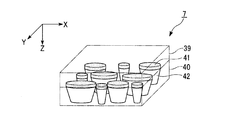
- It is a perspective view of the light-diffusion member with which a liquid crystal display device is provided.
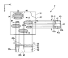
- It is a block diagram of a light diffusing member.
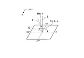
- FIG. 4 is a schematic diagram for explaining a relationship between a polar angle and an azimuth angle on a screen of a liquid crystal panel included in the liquid crystal display device.
- FIG. 3 is a schematic diagram showing azimuth angles between a horizontal direction and a vertical direction on a screen of a liquid crystal panel included in the liquid crystal display device.
- FIG. 4 is a schematic diagram showing a relationship between an azimuth angle direction where the diffusibility of the light diffusing member is relatively strong and the transmission axis of the polarizing plate. It is a side view which shows an example of the manufacturing apparatus of a light-diffusion member equally. It is a flowchart which shows the manufacturing process of a light-diffusion member similarly.
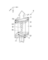
- FIG. 6 is another configuration diagram of the light diffusing member. It is a perspective view of the inspection apparatus shown as a 1st embodiment of the present invention.
- FIG. 1 is a cross-sectional view showing a schematic configuration of the liquid crystal display device 1.
- the liquid crystal display device 1 schematically includes a backlight 2, a first polarizing plate 3, a liquid crystal panel 4, a second polarizing plate 5, and a light diffusing member 7.
- the backlight 2, the first polarizing plate 3, the liquid crystal panel 4, and the second polarizing plate 5 constitute a liquid crystal display body 6.
- the light diffusing member 7 is bonded to the liquid crystal display body 6 on the second polarizing plate 5 side through the adhesive layer 8.
- the side on which the light diffusing member 7 is disposed is referred to as the viewing side
- the side on which the backlight 2 is disposed is referred to as the back side.
- the x-axis indicates the horizontal direction of the screen of the liquid crystal panel 4
- the y-axis indicates the vertical direction of the screen of the liquid crystal panel 4
- the z-axis indicates the thickness direction of the liquid crystal panel 4.
- the backlight 2 includes a light source 36 made of, for example, a light emitting diode or a cold cathode tube, and a light guide 37 that emits light toward the liquid crystal panel 4 using internal reflection of light emitted from the light source 36. Yes.
- the light source 36 is disposed on the end face of the light guide 37 (referred to as an edge light type).
- the light source 36 may be configured to be disposed directly below the light guide 37 (referred to as a direct type).
- the light guide 37 has a function of guiding light emitted from the light source 36 to the liquid crystal panel 4.
- a resin material such as acrylic resin is used.
- the light incident on the end surface of the light guide 37 from the light source 36 propagates while being totally reflected inside the light guide 37 and is emitted from the upper surface (light emission surface) of the light guide 37 with a substantially uniform intensity.
- a scattering sheet and a prism sheet are disposed on the upper surface of the light guide 37.
- the light emitted from the upper surface of the light guide 37 is scattered by the scattering sheet, then condensed by the prism sheet, and is emitted after being substantially parallelized.
- the prism sheet for example, BEF (trade name) manufactured by Sumitomo 3M is used.
- a backlight in which directivity is set moderately to some extent by controlling the light emission direction is suitably used as the backlight 2.
- the backlight 2 it does not necessarily prevent using what gave directionality (directional backlight).
- the first polarizing plate 3 functions as a polarizer and is disposed between the backlight 2 and the liquid crystal panel 4.
- the second polarizing plate 5 functions as an analyzer and is disposed between the liquid crystal panel 4 and the light diffusion member 7.
- the first polarizing plate 3 and the second polarizing plate 5 are arranged so that their polarization axes (transmission axes) are orthogonal (referred to as crossed Nicols).
- the liquid crystal panel 4 is a transmissive liquid crystal panel, for example. Further, the liquid crystal panel 4 is not limited to the transmissive type, and may be a transflective type (transmissive / reflective type) or a reflective type liquid crystal panel.
- the liquid crystal panel 4 is an active matrix type liquid crystal panel, and includes a thin film transistor (TFT) as a switching element for switching the operation of each pixel.
- TFT thin film transistor
- the liquid crystal panel 4 is not limited to the active matrix type, and may be a simple matrix type liquid crystal panel that does not include a switching element.
- the light diffusing member 7 expands the viewing angle by diffusing light emitted from the viewing side of the liquid crystal panel 4 (viewing angle widening film).
- the light emitted from the backlight 2 is modulated by the liquid crystal panel 4, and a predetermined image, characters, or the like is displayed by the modulated light. Further, when the light emitted from the liquid crystal panel 4 passes through the light diffusing member 7 and is emitted, the angular distribution of the emitted light becomes wider than before entering the light diffusing member 7. Thereby, the observer can visually recognize the display with a wide viewing angle.
- FIG. 2 is a cross-sectional view showing a schematic configuration of the liquid crystal panel 4.
- the liquid crystal panel 4 includes a TFT substrate (also referred to as an element substrate) 9, a color filter substrate (also referred to as a counter substrate) 10 disposed to face the TFT substrate 9, and a TFT substrate 9. And a liquid crystal layer 11 disposed between the color filter substrate 10 and the color filter substrate 10.
- a TFT substrate also referred to as an element substrate
- a color filter substrate also referred to as a counter substrate
- a liquid crystal layer 11 disposed between the color filter substrate 10 and the color filter substrate 10.
- the liquid crystal layer 11 seals the periphery between the TFT substrate 9 and the color filter substrate 10 with a seal member (not shown), and injects liquid crystal therebetween, thereby the TFT substrate 9 and the color filter substrate 10. Is sandwiched between.
- a spherical spacer 12 is disposed between the TFT substrate 9 and the color filter substrate 10 in order to keep the distance therebetween constant.
- the liquid crystal panel 4 of this embodiment performs display in, for example, a TN (TwistedistNematic) mode, and a TN liquid crystal is used for the liquid crystal layer 11.
- the display mode is not limited to the TN mode, and for example, a VA (Vertical Alignment) mode, an STN (Super Twisted Nematic) mode, an IPS (In-Plane Switching) mode, or the like can be used.
- the TFT substrate 9 has a plurality of pixels (not shown), which are the minimum unit areas for display, arranged in a matrix.
- a plurality of source bus lines (not shown) are formed on the TFT substrate 9 so as to extend in parallel with each other, and a plurality of gate bus lines (not shown) extend in parallel with each other. And formed so as to be orthogonal to the plurality of source bus lines. Therefore, on the TFT substrate 9, a plurality of source bus lines and a plurality of gate bus lines are formed in a lattice pattern, and a rectangular region partitioned by adjacent source bus lines and adjacent gate bus lines is one. One pixel.
- the source bus line is connected to the source electrode of the TFT described later, and the gate bus line is connected to the gate electrode of the TFT.
- a TFT 19 having a semiconductor layer 15, a gate electrode 16, a source electrode 17, a drain electrode 18, etc. is formed on the surface of the transparent substrate 14 constituting the TFT substrate 9 on the liquid crystal layer 11 side.
- a transparent substrate 14 for example, a glass substrate can be used.
- a semiconductor material such as CGS (Continuous Grain Silicon), LPS (Low-temperature Poly-Silicon), ⁇ -Si (Amorphous Silicon) is used.
- a semiconductor layer 15 is formed.
- a gate insulating film 20 is formed on the transparent substrate 14 so as to cover the semiconductor layer 15.
- a material of the gate insulating film 20 for example, a silicon oxide film, a silicon nitride film, or a laminated film thereof is used.
- a gate electrode 16 is formed on the gate insulating film 20 so as to face the semiconductor layer 15.
- a laminated film of W (tungsten) / TaN (tantalum nitride), Mo (molybdenum), Ti (titanium), Al (aluminum), or the like is used.
- a first interlayer insulating film 21 is formed on the gate insulating film 20 so as to cover the gate electrode 16.
- the material of the first interlayer insulating film 21 for example, a silicon oxide film, a silicon nitride film, or a laminated film thereof is used.
- a source electrode 17 and a drain electrode 18 are formed on the first interlayer insulating film 21.
- the source electrode 17 is connected to the source region of the semiconductor layer 15 through a contact hole 22 that penetrates the first interlayer insulating film 21 and the gate insulating film 20.
- the drain electrode 18 is connected to the drain region of the semiconductor layer 15 through a contact hole 23 that penetrates the first interlayer insulating film 21 and the gate insulating film 20.
- the same conductive material as that for the gate electrode 16 is used.
- a second interlayer insulating film 24 is formed on the first interlayer insulating film 21 so as to cover the source electrode 17 and the drain electrode 18.
- the same material as the first interlayer insulating film 21 described above or an organic insulating material is used.
- a pixel electrode 25 is formed on the second interlayer insulating film 24.
- the pixel electrode 25 is connected to the drain electrode 18 through a contact hole 26 that penetrates the second interlayer insulating film 24. That is, the pixel electrode 25 is connected to the drain region of the semiconductor layer 15 using the drain electrode 18 as a relay electrode.
- a transparent conductive material such as ITO (Indium Tin Oxide) or IZO (Indium Zinc Oxide) is used.
- an alignment film 27 is formed over the entire surface so as to cover the pixel electrode 25.
- This alignment film 27 has an alignment regulating force for vertically aligning liquid crystal molecules constituting the liquid crystal layer 11.
- the form of the TFT may be a top gate TFT shown in FIG. 2 or a bottom gate TFT.
- a black matrix 30, a color filter 31, a planarizing layer 32, a counter electrode 33, and an alignment film 34 are sequentially formed on the surface of the transparent substrate 29 constituting the color filter substrate 10 on the liquid crystal layer 11 side.
- the black matrix 30 has a function of blocking light transmission in the inter-pixel region, and is a photo in which metal such as Cr (chromium) or Cr / Cr oxide multilayer film or carbon particles are dispersed in a photosensitive resin. It is made of resist.
- the color filter 31 includes dyes of red (R), green (G), and blue (B), and one pixel electrode 25 on the TFT substrate 9 is any one of R, G, and B. Two color filters 31 are arranged to face each other.
- the color filter 31 may have a multicolor configuration of three or more colors of R, G, and B.
- the flattening layer 32 is made of an insulating film that covers the black matrix 30 and the color filter 31, and has a function of smoothing and flattening a step formed by the black matrix 30 and the color filter 31.
- a counter electrode 33 is formed on the planarization layer 32. As the material of the counter electrode 33, a transparent conductive material similar to that of the pixel electrode 25 is used. In addition, an alignment film 34 having a vertical alignment regulating force is formed on the entire surface of the counter electrode 33.
- FIG. 3A and 3B are schematic diagrams for explaining the operation of the liquid crystal panel 4.
- FIG. 3A is a diagram showing a state when no voltage is applied to the liquid crystal panel 4 (between the pixel electrode 25 and the counter electrode 33 shown in FIG. 2) (when no voltage is applied).
- FIG. 3B is a diagram illustrating a state when a certain voltage is applied to the liquid crystal panel 4 (when a voltage is applied).
- the symbol M is a liquid crystal molecule constituting the liquid crystal layer 11.
- the transmission axis P1 of the first polarizing plate 3 and the transmission axis of the second polarizing plate 5 are arranged in a crossed Nicols manner.
- the liquid crystal molecules M are twisted by 90 ° between the alignment film 27 and the alignment film 34 (see symbols H1 and H2).
- the polarization plane of the linearly polarized light LP1 transmitted through the first polarizing plate 3 having the transmission axis P1 in the 135 ° -315 ° direction is rotated by 90 ° due to the optical rotation of the liquid crystal layer 11.
- the linearly polarized light LP1 transmitted through the first polarizing plate 3 is transmitted through the second polarizing plate 5 having the transmission axis P2 in the 45 ° -225 ° direction.
- white display is obtained when no voltage is applied.
- the liquid crystal molecules M rise in a direction along the electric field between the alignment film 27 and the alignment film 34 as shown in FIG. 3B.
- the polarization plane of the linearly polarized light transmitted through the first polarizing plate 3 having the transmission axis P1 in the 135 ° -315 ° direction does not rotate.
- the linearly polarized light transmitted through the first polarizing plate 3 does not pass through the second polarizing plate 5 having the transmission axis P2 in the 45 ° -225 ° direction.
- black is displayed when a voltage is applied.
- the liquid crystal panel 4 can switch between white display and black display by controlling application / non-application of voltage for each pixel and display an image.
- the TFT substrate 9 and the color filter substrate 10 are respectively produced. Thereafter, the surface of the TFT substrate 9 on which the TFT 19 is formed and the surface of the color filter substrate 10 on which the color filter 31 is formed are arranged to face each other, and the TFT substrate 9 and the color filter substrate 10 are sealed. Paste through. Thereafter, liquid crystal is injected into a space surrounded by the TFT substrate 9, the color filter substrate 10, and the seal member. And the 1st polarizing plate 3 and the 2nd polarizing plate 5 are each bonded together on both surfaces of the liquid crystal panel 4 produced in this way using an optical adhesive agent.
- the liquid crystal display body 6 is manufactured through the above processes.
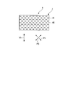
- FIG. 4 is a perspective view of the light diffusing member 7 viewed from the viewing side.
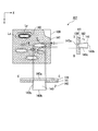
- FIG. 5 is a schematic diagram showing the configuration of the light diffusing member 7.
- the upper left side in FIG. 5 shows a plan view of the light diffusing member 7.
- the lower left side in FIG. 5 shows a cross-sectional view along the line AA in the plan view of the upper left side.
- the upper right side in FIG. 5 shows a cross-sectional view along the line BB in the plan view of the upper left side.
- the light diffusing member 7 includes a light-transmitting base material 39, a light diffusing portion 40 formed on one surface of the base material 39 (a surface opposite to the viewing side), and a light shielding layer (light absorbing portion) 41.
- the light-shielding layer 41 is separated into a plurality of regions and arranged in a region where the light diffusion portion 40 is formed.
- the base material 39 for example, a transparent resin film such as a triacetyl cellulose (TAC) film, polyethylene terephthalate (PET), polycarbonate (PC), polyethylene naphthalate (PEN), or polyethersulfone (PES) film is used.
- TAC triacetyl cellulose
- PET polyethylene terephthalate
- PC polycarbonate
- PEN polyethylene naphthalate
- PES polyethersulfone
- the base material 39 is a base for later forming the light shielding layer 41 and the light diffusing portion 40 in the manufacturing process described later, and needs to have heat resistance and mechanical strength in a heat treatment step during the manufacturing process. There is. Therefore, as the base material 39, a glass base material or the like may be used in addition to the resin base material. However, the thickness of the base material 39 is preferably as thin as possible without impairing the heat resistance and mechanical strength.
- the thickness of the base material 39 is increased, there is a possibility that display blur may occur.
- a transparent resin film having a thickness of 100 ⁇ m is used as an example of the base material 39.
- the total light transmittance of the substrate 39 is preferably 90% or more in accordance with JIS K7361-1. By setting the total light transmittance to 90% or more, sufficient transparency can be obtained.
- the light diffusing unit 40 is made of an organic material having light transmissivity and photosensitivity such as acrylic resin or epoxy resin.
- the total light transmittance of the light diffusing section 40 is preferably 90% or more as defined in JIS K7361-1. When the total light transmittance is 90% or more, sufficient transparency can be obtained.
- the light diffusing unit 40 has a light emitting end surface 40a, a light incident end surface 40b, and a side surface 40c.
- the light emission end surface 40 a is a surface in contact with the base material 39.
- the light incident end surface 40b is a surface facing the light emitting end surface 40a.
- the side surface 40c is a surface formed between the light emitting end surface 40a and the light incident end surface 40b.
- the area of the light incident end face 40b is larger than the area of the light emitting end face 40a. That is, the area of the horizontal cross section of the light diffusing portion 40 gradually increases from the base material 39 side to the side opposite to the base material 39. Therefore, the side surface 40c of the light diffusing portion 40 is an inclined surface inclined in a reverse taper shape from the base material 39 side toward the side opposite to the base material 39.
- the light diffusion part 40 is a part that contributes to the transmission of light in the light diffusion member 7. That is, the light incident from the light incident end face 40b of the light diffusing portion 40 is totally reflected by the side surface 40c of the light diffusing portion 40 and guided in a state of being substantially confined inside the light diffusing portion 40, and the light exit end face. Injected from 40a.
- the angle (hereinafter referred to as taper angle) formed by the side surface 40c with respect to the light incident end surface 40b is preferably 75 ° or more and 85 ° or less. In the present embodiment, the taper angle of the side surface 40c is 85 °. However, the taper angle of the side surface 40c is not particularly limited as long as it is an angle capable of sufficiently diffusing incident light when emitted from the light diffusion member 7. In the present embodiment, the taper angle of the side surface 40c is constant.
- the height from the light incident end surface 40 b to the light emitting end surface 40 a of the light diffusion portion 40 is set to be larger than the layer thickness of the light shielding layer 41.
- the layer thickness of the light shielding layer 41 is about 150 nm as an example.
- the height from the light incident end surface 40b of the light diffusing portion 40 to the light emitting end surface 40a is, for example, about 20 ⁇ m.
- the light shielding layer 41 is randomly arranged as viewed from the normal direction of the main surface of the base material 39.
- the light shielding layer 41 is made of, for example, a black resin containing carbon, an organic material having light absorption and photosensitivity such as black resist and black ink.
- a metal film such as Cr (chromium) or a Cr / Cr oxide multilayer film may be used.
- the light diffusion member 7 has a plurality of hollow portions 42.
- the hollow portion 42 is a portion surrounded by the side surface 40 c of the light diffusing portion 40 and the light shielding layer 41, and air exists in the hollow portion 42.
- the light diffusing part 40 is continuously provided in a part other than the plurality of hollow parts 42.
- the refractive index of the base material 39 and the refractive index of the light diffusing portion 40 are substantially equal.
- the reason is as follows. For example, consider a case where the refractive index of the base material 39 and the refractive index of the light diffusing portion 40 are greatly different. In this case, when light incident from the light incident end surface 40 b is emitted from the light emitting end surface 40 a, unnecessary light refraction or reflection may occur at the interface between the light diffusion portion 40 and the base material 39. In this case, there is a possibility that problems such as failure to obtain a desired viewing angle and a decrease in the amount of emitted light may occur.
- the light diffusion portion 40 is formed of, for example, a transparent acrylic resin
- the side surface 40c of the light diffusion portion 40 is an interface between the transparent acrylic resin and air.
- the hollow portion 42 may be filled with another low refractive index material.
- the difference in the refractive index at the interface between the inside and the outside of the light diffusing unit 40 is maximized when air is present rather than when any low refractive index material is present outside. Therefore, from Snell's law, in the configuration of the present embodiment, the critical angle is the smallest, and the incident angle range in which light is totally reflected by the side surface 40c of the light diffusing unit 40 is the widest. As a result, light loss is further suppressed, and high luminance can be obtained.
- the plurality of light shielding layers 41 are provided scattered on one surface of the base material 39.
- the planar shape of the light shielding layer 41 as viewed from the normal direction of the substrate 39 is an elongated ellipse. Further, a portion corresponding to the lower side of the light shielding layer 41 is an elliptic frustum-shaped hollow portion 42.
- the light shielding layer 41 has a major axis and a minor axis.
- the long axis is the longest axis in the planar shape of the light shielding layer 41 viewed from the normal direction of the base material 39.
- the short axis is the shortest axis in the planar shape of the light shielding layer 41 as viewed from the normal direction of the substrate 39.
- the ratio of the length of the short axis to the length of the long axis in each light shielding layer 41 is substantially equal.
- the major axis direction of the ellipse that forms the planar shape of each light shielding layer 41 (hereinafter, sometimes referred to as the major axis direction of the light shielding layer) is generally aligned in the X direction.
- the minor axis direction of the ellipse that forms the planar shape of each light shielding layer 41 (hereinafter sometimes referred to as the minor axis direction of the light shielding layer) is generally aligned in the Y direction.
- the ratio of the side surface 40c along the X direction in the side surface 40c of the light diffusing unit 40 is larger than the ratio of the side surface 40c along the Y direction. Therefore, the light Ly reflected by the side surface 40c along the X direction and diffused in the Y direction is larger than the light Lx reflected by the side surface 40c along the Y direction and diffused in the X direction. Therefore, the azimuthal direction in which the diffusibility of the light diffusing member 7 is the strongest is the Y direction that is the minor axis direction of the light shielding layer 41.
- the angle formed by the observer's line-of-sight direction F with respect to the normal direction E of the screen of the liquid crystal panel 4 included in the liquid crystal display device 1 is defined as a polar angle ⁇ .
- the angle formed by the direction of the line segment G when the line-of-sight direction F of the observer is projected on the screen with reference to the positive direction (0 ° direction) of the x-axis is defined as an azimuth angle ⁇ .
- FIG. 6 is a schematic diagram for explaining the relationship between the polar angle ⁇ and the azimuth angle ⁇ .
- the front shape of the screen of the liquid crystal panel 4 included in the liquid crystal display device 1 is a rectangle that is long in the left-right direction (horizontally long).
- the horizontal direction on this screen is defined as the direction of azimuth ⁇ : 0 ° -180 °.
- the direction of the azimuth angle ⁇ : 0 ° -180 ° is a horizontal direction (X direction) along an axis horizontal to the ground.
- the vertical direction on this screen is the azimuth angle ⁇ : 90 ° -270 °.
- the direction of the azimuth angle ⁇ : 90 ° -270 ° is the vertical direction (Y direction) along an axis perpendicular to the ground.
- FIG. 7 is a schematic diagram showing the horizontal direction and the vertical direction on the screen of the liquid crystal panel 4 included in the liquid crystal display device 1 by the azimuth angle ⁇ .
- FIG. 8 is a schematic diagram showing the relationship between the azimuth angle direction Vs in which the diffusibility of the light diffusing member 7 is relatively strong and the transmission axis P1 of the first polarizing plate 3 and the transmission axis P2 of the second polarizing plate 5.
- FIG. 8 the case where the some light shielding layer 41 is regularly arrange
- the azimuth angle direction Vs where the diffusibility of the light diffusing member 7 is relatively strong is the azimuth angle ⁇ on the screen of the liquid crystal panel 4: 90 ° -270.
- the direction is the ° direction (Y direction).
- the azimuth angle direction Vs where the diffusibility of the light diffusing member 7 becomes relatively strong the transmission axis P1 of the first polarizing plate 3 and the transmission of the second polarizing plate 5.
- the axis P2 is set so as to form an angle of approximately 45 °.
- the deviation in the rotational direction of the alignment between the liquid crystal panel and the polarizing plate is within about 5 °. Therefore, it can be said that the azimuth angle direction Vs in which the diffusibility of the light diffusing member 7 is relatively strong and the short side of the base material 39 are approximately parallel to each other are approximately parallel.
- the light diffusing member 7 is not necessarily limited to the above-described configuration in which the azimuth angle direction of the light diffusing portion 40 is aligned in one direction.
- the viewing angle characteristic improving direction of the liquid crystal panel 4 can be diversified by changing the azimuth angle direction of the azimuth anisotropy.
- the light diffusing member 7 having the above configuration is disposed on the viewing side of the liquid crystal display body 6 as shown in FIG. That is, the light diffusion portion 40 is bonded to the second polarizing plate 5 through the adhesive layer 8 with the base material 39 on the outermost surface facing the viewing side.
- FIG. 9 is a side view showing the configuration of the manufacturing apparatus 50 for the light diffusing member 7.
- FIG. 10 is a flowchart showing a manufacturing process of the light diffusing member 7.
- the manufacturing apparatus 50 includes a conveying device that conveys a long base sheet (raw sheet) 39 ⁇ / b> A that is a raw sheet of the base material 39 by roll-to-roll (RtoR), And a processing device for performing various processes.
- the manufacturing process of the light-diffusion member 7 using this manufacturing apparatus 50 includes the conveyance process which conveys the base material sheet 39A, and the process process which performs various processes while conveying the base material sheet 39A.
- the feeding roller 51 for feeding the base sheet 39A is provided on one end side, and the winding roller 52 for winding the base sheet 39A is provided on the other end side.
- the base sheet 39A is transported (moved) from the side toward the winding roller 52 side.
- a printing device 53, a bonding device 54, an exposure device 55, a developing device 56, and a drying device are arranged in the middle of the conveyance direction of the base sheet 39A from the sending roller 51 side to the winding roller 52 side.
- Various processing devices including a curing device 57 and a curing device 58, and an inspection device 60 are sequentially arranged.
- the printing device 53 forms a plurality of light shielding layers 41 on the base sheet 39A by gravure printing.
- the bonding apparatus 54 bonds a negative dry film resist (photosensitive resin layer) DFR on the base sheet 39A on which the plurality of light shielding layers 41 are formed.
- the exposure device 55 irradiates the exposure light F from the base material sheet 39A side to expose the dry film resist DFR.
- the developing device 56 develops the dry film resist DFR after exposure with the developer DL.
- the drying device 57 performs drying of the base sheet 39A on which the light diffusion portion 40 made of the dry film resist DFR after development is formed.
- the curing device 58 irradiates the base material sheet 39A on which the light diffusing unit 40 is formed with ultraviolet light (UV light) F 'to cure (post-cure) the light diffusing unit 40.
- the inspection device 60 inspects the state of the light diffusion portion 40 and the light shielding layer 41 formed on the base sheet 39A.
- step S1 shown in FIG. 10 a plurality of light shielding layers 41 are formed on one surface of the base sheet 39A by gravure printing.
- the light shielding layer 41 becomes a light shielding layer 41 while rotating the printing roller 53 a included in the printing device 53 on the surface of the base material sheet 39 ⁇ / b> A in the same direction as the transport direction of the base material sheet 39 ⁇ / b> A. Transfer the layer material.
- the some light shielding layer 41 can be collectively formed in one surface of 39 A of base material sheets.
- the planar shape of the light shielding layer 41 is elliptical, and the thickness of the light shielding layer 41 is 150 nm. Further, in the region other than the light shielding layer 41, an opening 41a corresponding to the formation region of the light diffusion portion 40 in the next process is formed.
- the arrangement of the intervals (pitch) between the adjacent light shielding layers 41 is neither regular nor periodic.
- the interval (pitch) between the light shielding layers 41 is preferably smaller than the interval (pitch, for example, 150 ⁇ m) between the pixels of the liquid crystal panel 2. Thereby, at least one light shielding layer 41 is formed in the pixel. Therefore, for example, when combined with a liquid crystal panel having a small pixel pitch used for a mobile device or the like, a wide viewing angle can be achieved.
- the light shielding layer 41 is formed using gravure printing.
- a printing method such as gravure offset printing may be used.
- the light shielding layer 41 may be formed by a photolithography method using a black negative resist. In this case, if a photomask in which the opening pattern and the light shielding pattern are reversed is used, a positive resist having a light absorption property can also be used.
- the light shielding layer 41 may be directly formed using a vapor deposition method, an inkjet method, or the like.
- a dry film resist DFR is bonded onto the base sheet 39A on which the plurality of light shielding layers 41 are formed.
- the dry film resist DFR is sent out from the feed roller 54 a included in the bonding device 54, and the bonding roller 54 b is rotated in the same direction as the conveyance direction of the base sheet 39 ⁇ / b> A,
- a dry film resist DFR having a thickness of about 20 ⁇ m is bonded.
- an intermediate body in which a plurality of light shielding layers 41 and a dry film resist (photosensitive resin layer) DFR covering the surface on which the light shielding layers 41 are formed are formed on one surface of the base material sheet 39A (base material 39). 100A can be obtained.
- the exposure light F suitable for exposing the dry film resist DFR.
- the dry film resist DFR is exposed radially so as to spread outward from the non-formation region (opening 41a) of the light shielding layer 41 by the diffused exposure light F.
- the side surface 40c of the light-diffusion part 40 can be made into the inclined surface inclined in reverse taper shape toward the opposite side to the base material 39 from the base material 39 side.
- strength of the exposure light F may change, for example, the intensity
- the emission angle of the exposure light F may gradually change as the base sheet 39A advances.
- the exposure light F may be light obtained by diffusing parallel light with a diffusion plate. Thereby, the taper angle of the side surface 40c of the light diffusion part 40 can be controlled to a desired angle.
- step S4 shown in FIG. 10 development is performed on the dry film resist DFR after exposure.
- the developing device 56 applies the developer DL to the dry film resist DFR after exposure.
- the unexposed part of the dry film resist DFR is removed, and the light diffusion part 40 is formed on one surface of the base sheet 39A.
- step S5 shown in FIG. 10 the base sheet 39A on which the light diffusion portion 40 is formed is dried.
- the drying device 57 blows hot air H of 100 ° C. from the light diffusion portion 40 side of the base sheet 39 ⁇ / b> A to dry (post-bake) the light diffusion portion 40.
- step S6 shown in FIG. 10 the light diffusion unit 40 is cured (post-cure). Specifically, as illustrated in FIG. 9, ultraviolet light (UV light) F ′ emitted from a plurality of light sources 58 a included in the curing device 58 is irradiated from the light diffusion portion 40 side of the base sheet 39 ⁇ / b> A to diffuse the light. The part 40 is cured.
- UV light ultraviolet light
- step S7 shown in FIG. 10 the state of the light diffusion portion 40 and the light shielding layer 41 formed on the base sheet 39A is inspected.
- the light source unit 60a is on one side (the upper side in FIG. 9) sandwiching the base sheet 39A. It arrange
- the light source unit 60a irradiates the measurement light ML to the base sheet 39A, and the light detection unit 60b detects the measurement light ML transmitted through the base sheet 39A. Then, based on the detection result of the measurement light ML detected by the light detection unit 60b, the states of the light diffusion unit 40 and the light shielding layer 41 are inspected.
- a step of recording inspection information for example, presence / absence of defect, position, type
- information regarding the position and type of a defective portion for example, a portion with low luminance
- a recording device for recording such inspection information on the base sheet 39A for example, a labeler (seal sticking device) for attaching a label on which defect information is written, or defect information is recorded by ejecting ink.
- An inkjet apparatus that performs the above, a laser marker that records defect information by laser irradiation, and the like can be used.
- the manufacturing apparatus 50 of the light diffusing member 7 not only when defect information is physically recorded on the base sheet 39A using the recording apparatus described above, but also based on the defect information detected by the inspection apparatus 60. You may make it control the processing apparatus which performs various processes with respect to the base material sheet 39A.
- the defect information detected by the inspection device 60 is temporarily stored (accumulated) in an information storage device such as a server. Thereafter, a control signal based on the defect information is transmitted to the target processing device. Thereby, the processing conditions for the base sheet 39A can be changed, and as a result, quality improvement and yield improvement can be achieved.
- the long light diffusion member 7 can be obtained through the above steps.
- the light diffusing member 7 is wound on the winding roller 52 by a predetermined amount, and then sent to the next step.
- the light diffusing portion 40 in the step of forming the light diffusing portion 40, since the exposure light F is irradiated using the light shielding layer 41 as a mask, the light diffusing portion 40 is self-aligned with the position of the opening 41a of the light shielding layer 41 ( It is formed in a self-aligned state. As a result, the light diffusing unit 40 and the light shielding layer 41 are in close contact with each other, so that no gap is formed between them, and the light transmittance can be reliably maintained. In addition, since precise alignment work is unnecessary, the time required for manufacturing can be shortened.
- a step of attaching an optical sheet to be the second polarizing plate 5 to the light diffusing member 7 obtained through the above steps may be provided.
- the light-diffusion member 7 can also be formed integrally with the second polarizing plate 5.
- the produced light diffusing member 7 is cut into a predetermined size according to the liquid crystal panel 4 and then bonded to the liquid crystal display body 6. That is, the light diffusing member 7 is attached to the second polarizing plate 5 via the adhesive layer 8 with the base material 39 facing the viewing side and the light diffusing portion 40 facing the second polarizing plate 5. Combined.
- the liquid crystal display device 1 can be manufactured through the steps as described above.
- the planar shape of the light shielding layer 41 may include various shapes such as a circle, a polygon, and a semicircle in addition to the above-described ellipse. Further, a part of the light shielding layer 41 may be formed to overlap.
- the light diffusing unit 140 may be divided into a plurality of regions in the region where the light shielding layer 141 is formed.
- the light diffusing unit 140 has a light emitting end surface 140a, a light incident end surface 140b, and a side surface 140c.
- a space 142 is formed between the light diffusion unit 140 and the light shielding layer 141, and an air layer exists in the space 142.
- the light incident from the light incident end surface 140 b of the light diffusing portion 140 is totally confined inside the light diffusing portion 140 while being totally reflected by the side surface 140 c of the light diffusing portion 140. And is emitted from the light exit end face 140a.
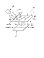
- FIG. 12 is a perspective view showing a schematic configuration of the inspection apparatus 160.
- the inspection device 160 inspects the state of the light diffusion portion 40 and the light shielding layer 41 of the light diffusion member 7, and can be applied to the inspection device 60 of the manufacturing apparatus 50 shown in FIG. 9 described above. That is, the inspection device 160 uses the light formed on the base sheet 39 ⁇ / b> A that becomes the raw sheet of the light diffusing member 7 when the light diffusing member 7 is produced by a roll-to-roll (RtoR) method. It is possible to inspect the states of the diffusing unit 40 and the light shielding layer 41.
- the inspection device 160 includes a light source unit 161 and a light detection unit 162 as shown in FIG.
- the light source unit 161 is disposed on one side of the light diffusion member 7 and irradiates the measurement light ML to the light diffusion member 7.
- the light detection unit 162 is disposed on the other side of the light diffusion member 7 and detects the measurement light ML transmitted through the light diffusion member 7.
- the light source unit 161 has a surface side (not shown in FIG. 12) facing the light diffusion unit 40 and the light shielding layer 41 (not shown in FIG. 12) formed on one surface of the base material 39 with the light diffusion member 7 interposed therebetween. 12 on the lower side). Further, the light detection unit 162 is disposed on the surface side (upper side in FIG. 12) facing the other surface of the base material 39 with the light diffusion member 7 interposed therebetween.
- the light source unit 161 is disposed on the upper side with the base sheet 39A interposed therebetween, and the light detection unit 162 is disposed on the lower side with the base sheet 39A interposed therebetween. What is necessary is just to arrange
- the light source unit 161 is disposed on the lower side with the base material sheet 39A interposed therebetween and the light detection unit 162 is disposed on the upper side with the light diffusion member 7 interposed therebetween, the light diffusion formed on the base material sheet 39A It is possible to inspect the state of the portion 40 and the light shielding layer 41.
- the light source unit 161 is configured by a surface light source device that irradiates the measurement light ML emitted in a planar shape.
- This surface light source device includes a TN liquid crystal panel 161a and an illumination device 161b that irradiates the liquid crystal panel 161a with illumination light, and irradiates the light diffusing member 7 with light emitted from the liquid crystal panel 161a as measurement light ML.
- a liquid crystal display device is used.
- the visible light may be, for example, short wavelength light such as red light, green light, or blue light, or multi-wavelength light such as white light.
- the light detection unit 162 is configured by a photodetector that detects the measurement light ML that has passed through the light diffusion member 7.
- a luminance meter that measures the luminance of the measurement light ML is used as the photodetector.
- Examples of the luminance meter include a color luminance meter and a spectral luminance meter.
- a light receiving element such as a photodiode (PD) or an image pickup element such as a CCD or CMOS can be used.
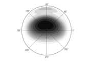
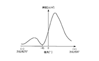
- FIG. 13 is a graph showing the luminance in the azimuth direction of the measurement light ML as an isoluminance curve.
- FIG. 14 is a graph showing a polar angle luminance distribution in a specific azimuth angle direction (azimuth angle 90 ° -270 ° direction) of the measurement light ML.
- the horizontal axis represents the polar angle [° (deg)]
- the vertical axis represents the standard when the luminance in the front direction of the light source unit 161 (polar angle 0 ° direction) is 1.
- the measurement light L has a polar angle luminance distribution in which the luminance with respect to the polar angle direction is different in a specific azimuth angle direction. Further, the measurement light ML has a polar angle luminance distribution in which the luminance with respect to the polar angle direction is relatively low on the side toward the light detection unit 162 (the side on which the polar angle is minus ( ⁇ )).
- the light diffusing member 7 measures the measurement light in the minor axis direction (azimuth angle 90 ° -270 ° direction) of the light shielding layer 41 rather than the long axis direction (azimuth angle 0 ° -180 ° direction) of the light shielding layer 41. It has azimuthal anisotropy that makes ML diffusibility relatively strong.
- the light source unit 161 has a specific azimuth angle direction (azimuth angle 90 ° -270 ° direction) of the measurement light ML and an azimuth angle at which the diffusibility of the measurement light ML of the light diffusing member 7 becomes relatively strong. It arrange
- the light detection unit 162 is arranged in a plane in the same direction as a specific azimuth angle direction (azimuth angle 90 ° -270 ° direction) of the measurement light ML. That is, the direction in which the light detection unit 162 is arranged coincides with the azimuth direction (the short axis direction of the light shielding layer 41) in which the diffusibility of the measurement light ML of the light diffusing member 7 is relatively strong. Further, the light detection unit 162 is disposed on the side where the luminance in the specific azimuth angle direction of the measurement light ML shown in FIG. 14 is relatively low (the side where the polar angle is minus ( ⁇ )).
- the light detection unit 162 has a predetermined value on the upstream side ( ⁇ 270 ° direction) in the transport direction within the plane along the transport direction MD of the light diffusion member 7 (azimuth angle 90 ° -270 ° direction). It is arranged inclined at an angle theta 2. That is, the normal line V 2 on the light receiving surface of the light detection unit 162 is inclined at a predetermined angle ⁇ 2 with respect to the normal line V 0 of the light diffusion member 7.
- the angle ⁇ 2 of the light receiving surface of the light detection unit 162 is preferably matched with the polar angle direction (valley position) where the luminance of the measurement light ML is minimum in the graph shown in FIG.
- the angle ⁇ 2 of the light receiving surface of the light detection unit 162 is set to 45 ° with respect to the normal line V 0 of the light diffusing member 7.
- the luminance of the measurement light ML in the polar angle ⁇ 45 ° direction is about 1/10 of the luminance in the polar angle 0 ° direction.
- the states of the light diffusion unit 40 and the light shielding layer 41 are inspected based on the detection result of the measurement light ML detected by the light detection unit 162.
- the light diffusing member 7 is transmitted from one surface side (lower side) to the other surface side (upper side) while the light diffusing member 7 is conveyed in the direction of 90 ° azimuth.
- the light detection unit 162 detects the measured light ML.
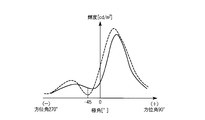
- FIG. 15 is a graph showing the luminance in the azimuth direction of the measurement light ML transmitted through the light diffusing member 7 as an isoluminance curve.
- FIG. 16 is a graph showing the polar angle luminance distribution in a specific azimuth angle direction (azimuth angle 90 ° -270 ° direction) of the measurement light ML transmitted through the light diffusing member 7.
- the luminance characteristics of the measurement light L change as it passes through the light diffusing member 7 as shown in FIGS. 15 and 16. Therefore, in the inspection of the light diffusing member 7 according to the present embodiment, the state of the light diffusing portion 40 (for example, the taper angle of the side surface 40c) or the state of the light blocking layer 41 (for example, the light blocking layer 41) is determined from the change in luminance characteristics. Etc.) can be inspected.
- the luminance of the measurement light ML transmitted through the light diffusing member 7 changes the most in the polar angle direction (valley position) at which the above-mentioned luminance is minimized. It is. That is, in this polar angle direction, the measurement light ML transmitted through the light diffusing member 7 greatly changes in the direction in which the luminance increases.
- the light diffusing member 7 is irradiated with the measurement light ML having different luminance depending on the direction, and the light detection unit 162 is disposed on the side where the luminance in the specific azimuth angle direction of the measurement light ML is relatively low.
- the detection angle and the detection accuracy of the measurement light ML can be greatly improved by aligning the angle ⁇ 2 of the light receiving surface of the light detection unit 162 with the polar angle direction in which the luminance of the measurement light ML is minimized. It is.
- the light diffusion characteristics of the light diffusing member 7 can be in-line inspected. It is possible to easily and accurately inspect the light diffusing member 7 while reducing labor and the like.
- the light diffusing member 7 is inspected according to the azimuthal anisotropy of the light diffusing member 7 described above, so that the liquid crystal panel 4 is actually visually recognized. It is possible to more directly grasp the light diffusion characteristics of the light diffusion member 7 required when the light diffusion member 7 is bonded to the side.
- the present invention is not necessarily limited to such a case.
- the case shown in FIGS. 17A and 17B may be used.
- FIG. 17A shows a case where the light diffusing member 7 in which the major axis direction of the light shielding layer 41 is coincident with the azimuth angle 90 ° -270 ° direction is conveyed in the azimuth angle 90 ° direction.
- the light source unit 161 has a specific azimuth angle direction (azimuth angle 0 ° -180 ° direction) of the measurement light ML and an azimuth angle direction (where the diffusibility of the measurement light ML of the light diffusion member 7 is relatively strong) What is necessary is just to arrange
- FIG. 17B shows a case where the light diffusing member 7 in which the major axis direction of the light shielding layer 41 coincides with the azimuth angle 135 ° -315 ° direction is conveyed in the azimuth angle 90 ° direction.
- the light source unit 161 has a specific azimuth angle direction (azimuth angle 45 ° -225 ° direction) of the measurement light ML and an azimuth angle direction (in which the diffusibility of the measurement light ML of the light diffusing member 7 becomes relatively strong ( What is necessary is just to arrange
- the light detection unit 162 is inclined in the upstream direction (azimuth angle 270 ° direction) in the transport direction within the plane of the light diffusion member 7 along the transport direction (azimuth angle 90 ° -270 ° direction).
- the present invention is not necessarily limited to the configuration arranged in this manner. That is, with respect to the direction in which the light detection unit 162 is arranged, the specific azimuth direction of the measurement light ML described above, or the azimuth direction in which the diffusibility of the measurement light ML of the light diffusion member 7 is relatively strong (light shielding layer). 41 in the direction of the minor axis) and can be set in any direction.
- the angle ⁇ 2 of the light receiving surface of the light detection unit 162 is not limited to the polar angle direction in which the luminance of the measurement light ML is minimized, and can be set to an arbitrary angle.
- the light detection unit 162 may be arranged to be movable in the azimuth angle direction or polar angle direction of the light diffusion member 7 described above.
- the light diffusing member 7 can be inspected from different azimuth and polar directions, and the light diffusing characteristics of the light diffusing member 7 can be inspected in more detail.
- the light detection part 162 may be arrange
- the light detectors 162 may be arranged at a plurality of locations in the azimuth angle direction or polar angle direction of the light diffusion member 7 described above.
- the light diffusing member 7 can be inspected simultaneously from different azimuth and polar directions, and the light diffusing characteristics of the light diffusing member 7 can be inspected in more detail and simultaneously.
- a plurality of the light detection units 162 may be arranged side by side in a direction that intersects the transport direction of the light diffusion member 7 described above. In this case, not only different positions in the surface of the light diffusing member 7 can be inspected simultaneously, but also variations in light diffusion characteristics in the surface of the light diffusing member 7 can be inspected simultaneously. Furthermore, even when the light detection units 162 are arranged at a plurality of locations, the plurality of light detection units 162 can be movable.
- FIG. 20 is a cross-sectional view illustrating a configuration of the light source unit 261 provided in the inspection apparatus 260.
- the inspection device 260 has basically the same configuration as the inspection device 160 except that the light source unit 261 is provided instead of the light source unit 161. Therefore, in the following description, the light source unit 261 illustrated in FIG. 20 is described.
- the light source unit 261 includes a light emitting element 262, a light guide 263 that emits light emitted from the light emitting element 262 in a planar shape, and a light diffusion that diffuses light from the light guide 263 in different directions.
- This is a surface light source device that irradiates the light diffusing member 7 with the light diffused by the light diffuser 264 as the measurement light ML.
- the light emitting element 262 for example, a light emitting diode (LED), a cold cathode tube (CCFL), or the like can be used.
- the light guide 263 is formed in a wedge shape, propagates light emitted from the light emitting element 262 attached to the proximal end surface thereof toward the distal side, and faces the light diffuser 264. By totally reflecting the light incident on the slope on the opposite side, the light is emitted from the surface facing the light diffuser 264 to the outside.
- the light diffusing body 264 includes a prism sheet in which a plurality of prism bodies 264 a are formed side by side on the surface facing the light guide 263.
- the light diffusing body 264 refracts the light from the light guide 263 by the plurality of prism bodies 264a, thereby emitting diffused light diffused in different directions from the surface opposite to the surface facing the light guide 263.
- the diffused light can be diffused in different directions by adjusting the angle of the inclined surface of the light guide 263 and the tip angle of the prism body 264 a of the light diffuser 264. Thereby, it is possible to obtain the measurement light ML whose luminance varies depending on the orientation described above.
- the light diffusing member 7 is inspected by the same procedure as the inspection apparatus 160 of the first embodiment except that the light source unit 261 is used instead of the light source unit 161. It can be carried out.
- the light diffusion characteristics of the light diffusing member 7 are in-line, similar to the inspection of the light diffusing member 7 by the inspection apparatus 160 of the first embodiment. Since it can be inspected, it is possible to easily and accurately inspect the light diffusing member 7 while reducing the time and labor required for the inspection of the light diffusing member 7.
- the light diffusing member 7 is inspected according to the azimuth anisotropy of the light diffusing member 7 described above, so that the liquid crystal panel 4 is actually visually recognized. It is possible to more directly grasp the light diffusion characteristics of the light diffusion member 7 required when the light diffusion member 7 is bonded to the side.
- 161 and 261 may be configured such that the normal line V 1 on the light emitting surface is inclined at a predetermined angle ⁇ 1 with respect to the normal line V 0 of the light diffusing member 7.
- the inspection device 160 and 260 by placing rotatably the light source unit 161, 261 about the axis of the normal V 1, or a variable specific azimuthal direction of the measurement light ML as described above, By arranging the light source units 161 and 261 to be tiltable, the angle ⁇ 1 of the measurement light ML incident on the light diffusing member 7 can be made variable.
- the technical scope of the present invention is not limited to the above embodiment, and various modifications can be made without departing from the spirit of the present invention.
- the light source unit may be configured by a plurality of light sources.
- the plurality of light sources may be configured to irradiate the light diffusing member 7 with measurement light having different wavelengths.
- each light source that emits red light, green light, and blue light
- the light diffusing member 7 can be inspected with different chromaticities.
- the present invention can be widely applied to a light diffusing member, a light diffusing member inspection apparatus, a manufacturing apparatus, and a manufacturing method that can be used in various display devices such as a liquid crystal display device, an organic electroluminescence display device, and a plasma display. is there.
Landscapes
- Physics & Mathematics (AREA)
- Nonlinear Science (AREA)
- General Physics & Mathematics (AREA)
- Optics & Photonics (AREA)
- Chemical & Material Sciences (AREA)
- Crystallography & Structural Chemistry (AREA)
- Engineering & Computer Science (AREA)
- Manufacturing & Machinery (AREA)
- Mathematical Physics (AREA)
- Optical Elements Other Than Lenses (AREA)
Abstract
光拡散部材は、光透過性を有する基材と、基材の一面に所定の高さで形成された光拡散部と、基材の一面のうち光拡散部以外の領域に光拡散部の高さよりも小さい厚みで形成された遮光層と、を有する。光拡散部が、基材に接する光射出端面と、光射出端面に対向し、光射出端面の面積よりも大きい面積を有する光入射端面と、を含む。光拡散部材内に情報が記録されている。
Description
本発明は、光拡散部材、光拡散部材の検査装置、並びに光拡散部材の製造装置及び製造方法に関する。
本願は、2013年11月5日に、日本に出願された特願2013-229669号に基づき優先権を主張し、その内容をここに援用する。
本願は、2013年11月5日に、日本に出願された特願2013-229669号に基づき優先権を主張し、その内容をここに援用する。
液晶表示装置は、例えば、携帯電話機等の携帯型電子機器や、テレビジョン、パーソナルコンピュータなどのディスプレイとして広く用いられている。ところで、液晶表示装置は、正面からの視認性に優れる反面、視野角が狭いといった特性を一般的に有している。
このため、液晶表示装置では、視野角を広げるための様々な工夫が従来より行われている。その工夫の一つとして、液晶パネル(表示体)の視認側に光拡散部材を配置し、この光拡散部材を用いて液晶パネルの視認側から射出される光を拡散させることが行われている。
このため、液晶表示装置では、視野角を広げるための様々な工夫が従来より行われている。その工夫の一つとして、液晶パネル(表示体)の視認側に光拡散部材を配置し、この光拡散部材を用いて液晶パネルの視認側から射出される光を拡散させることが行われている。
例えば下記特許文献1には、透明基材と、透明基材の一面に形成されたテーパー状の側面を有する光拡散部と、透明基材の一面における光拡散部材の形成領域以外の領域に形成された遮光層とを備えた光拡散部材が開示されている。この光拡散部材を製造する際は、遮光層が形成された透明基材の上に透明ネガレジストを塗布した後、遮光層をマスクとして透明基材側から紫外光(UV光)を照射する。これにより、透明ネガレジストをパターニングし、上述したテーパー状の側面を有する光拡散部が形成される。
ところで、光拡散部材の光拡散特性は、光拡散部の出来栄えに大きく影響を受ける。すなわち、所望の光拡散特性を得るためには、光拡散部の形状や寸法が当初の設計通りに仕上がっていることが重要である。
しかしながら、光拡散部材が所望の光拡散特性を有しているか否かについては、実際に液晶パネルの視認側に光拡散部材を貼り合わせた後、その表示特性を確認する方法を用いなければならず、ロール・ツー・ロール(RtoR)方式で連続的に製造される光拡散部材の光拡散特性をインラインで検査することができなかった。
本発明のいくつかの態様は、上記の課題を解決するためになされたものであり、光拡散部材の検査を容易に且つ正確に行うことができ、インラインによる検査にも対応可能な光拡散部材、光拡散部材の検査装置、並びにそのような検査装置を用いた光拡散部材の製造装置及び製造方法を提供することを目的の一つとする。
上記の目的を達成するために、本発明のいくつかの態様は以下の手段を採用した。
(1) 本発明の第1の態様に係る光拡散部材は、光透過性を有する基材と、前記基材の一面に所定の高さで形成された光拡散部と、前記基材の一面のうち前記光拡散部以外の領域に前記光拡散部の高さよりも小さい厚みで形成された遮光層と、を有し、前記光拡散部が、前記基材に接する光射出端面と、前記光射出端面に対向し、前記光射出端面の面積よりも大きい面積を有する光入射端面と、を含む光拡散部材であって、部材内に情報が記録されている。
(1) 本発明の第1の態様に係る光拡散部材は、光透過性を有する基材と、前記基材の一面に所定の高さで形成された光拡散部と、前記基材の一面のうち前記光拡散部以外の領域に前記光拡散部の高さよりも小さい厚みで形成された遮光層と、を有し、前記光拡散部が、前記基材に接する光射出端面と、前記光射出端面に対向し、前記光射出端面の面積よりも大きい面積を有する光入射端面と、を含む光拡散部材であって、部材内に情報が記録されている。
(2) 前記(1)に記載の光拡散部材において、前記情報が欠陥情報であってもよい。
(3) 前記(1)に記載の光拡散部材において、前記情報が不良箇所の位置や種類に関する情報であってもよい。
(4) 前記(1)に記載の光拡散部材において、前記記録の位置が不良箇所の位置と近接していてもよい。
(5) 前記(1)に記載の光拡散部材において、前記記録の位置が基材内の光拡散部が設けられていない領域にあってもよい。
(6) 本発明の第2の態様に係る光拡散部材の検査装置は、光透過性を有する基材と、前記基材の一面に所定の高さで形成された光拡散部と、前記基材の一面のうち前記光拡散部以外の領域に前記光拡散部の高さよりも小さい厚みで形成された遮光層と、を有し、前記光拡散部が、前記基材に接する光射出端面と、前記光射出端面に対向し、前記光射出端面の面積よりも大きい面積を有する光入射端面と、を含む光拡散部材の検査装置であって、前記光拡散部材を挟んだ一方側に配置されて、前記光拡散部材に対して方位によって輝度が異なる測定光を照射する光源部と、前記光拡散部材を挟んだ他方側に配置されて、前記光拡散部材を透過した測定光を検出する光検出部と、を備え、前記光検出部が検出した測定光の検出結果に基づいて、前記光拡散部及び前記遮光層の状態を検査する。
(7) 前記(6)に記載の光拡散部材の検査装置において、前記測定光は、特定の方位角方向において極角方向に対する輝度が異なった極角輝度分布を有していてもよい。
(8) 前記(7)に記載の光拡散部材の検査装置において、前記光拡散部材は、前記光拡散部の前記光射出端面と前記光入射端面との間に形成される側面のうち、その面積が大きくなる方位よりも、その面積が小さくなる方位において、前記測定光の拡散性が相対的に強くなる方位異方性を有し、前記光検出部は、前記測定光の特定の方位角方向と同一方向の面内に配置されていてもよい。
(9) 前記(8)に記載の光拡散部材の検査装置において、前記光源部は、前記測定光の特定の方位角方向と、前記光拡散部材の測定光の拡散性が相対的に強くなる方位角方向とを一致させた状態で配置され、前記測定光は、前記極角方向に対する輝度が前記光検出部に向かう側で相対的に低くなる極角輝度分布を有していてもよい。
(10) 前記(6)~(9)の何れかに記載の光拡散部材の検査装置において、前記光源部は、その発光面における法線が前記光拡散部材の法線に対して斜めとなる角度で配置されていてもよい。
(11) 前記(6)~(10)の何れかに記載の光拡散部材の検査装置において、前記光検出部は、複数箇所に配置されていてもよい。
(12) 前記(6)~(11)の何れかに記載の光拡散部材の検査装置において、前記光検出部は、移動自在に配置されていてもよい。
(13) 前記(6)~(12)の何れかに記載の光拡散部材の検査装置において、前記光源部は、前記測定光として可視域光を照射してもよい。
(14) 前記(6)~(12)の何れかに記載の光拡散部材の検査装置において、前記光源部は、複数の光源を有し、前記複数の光源がそれぞれ異なる波長の測定光を前記光拡散部材に対して照射してもよい。
(15) 前記(6)~(12)の何れかに記載の光拡散部材の検査装置において、前記光源部は、液晶パネルと、前記液晶パネルに照明光を照射する照明装置とを含み、前記測定光として、前記液晶パネルから射出された光を照射してもよい。
(16) 前記(6)~(12)の何れかに記載の光拡散部材の検査装置において、前記光源部は、発光素子と、前記発光素子が発する光を面状に発光させる導光体と、前記導光体からの光を異なる方位に拡散させる光拡散体と、を含み、前記測定光として、前記光拡散体により拡散された光を照射してもよい。
(17) 本発明の第3の態様に係る光拡散部材の製造装置は、光透過性を有する基材と、前記基材の一面に所定の高さで形成された光拡散部と、前記基材の一面のうち前記光拡散部以外の領域に前記光拡散部の高さよりも小さい厚みで形成された遮光層と、を有し、前記光拡散部が、前記基材に接する光射出端面と、前記光射出端面に対向し、前記光射出端面の面積よりも大きい面積を有する光入射端面と、を含む光拡散部材の製造装置であって、前記光拡散部材となる原反シートに対して各種の処理を行う処理装置と、前記原反シートの搬送を行う搬送装置と、前記原反シートに対する検査を行う検査装置と、を備え、前記検査装置が、前記(6)~(16)の何れかに記載の光拡散部材の検査装置を含む。
(18) 前記(17)に記載の光拡散部材の製造装置において、前記検査装置の検査結果に基づく検査情報を前記原反シートに記録する記録装置を備えていてもよい。
(19) 本発明の第4の態様に係る光拡散部材の製造方法は、光透過性を有する基材と、前記基材の一面に所定の高さで形成された光拡散部と、前記基材の一面のうち前記光拡散部以外の領域に前記光拡散部の高さよりも小さい厚みで形成された遮光層と、を有し、前記光拡散部が、前記基材に接する光射出端面と、前記光射出端面に対向し、前記光射出端面の面積よりも大きい面積を有する光入射端面と、を含む光拡散部材の製造方法であって、前記光拡散部材となる原反シートに対して各種の処理を行う処理工程と、前記前記原反シートの搬送を行う搬送工程と、前記原反シートに対する検査を行う検査工程と、を含み、前記検査工程において、前記(6)~(16)の何れかに記載の光拡散部材の検査装置を用いる。
(20) 前記(19)に記載の光拡散部材の製造方法において、前記検査工程での検査結果に基づく検査情報を前記原反シートに記録する記録工程を含んでいてもよい。
以上のように、本発明のいくつかの態様によれば、光拡散部材の検査を容易に且つ正確に行うことができ、インラインによる検査にも対応可能な光拡散部材、光拡散部材の検査装置、並びにそのような検査装置を用いた光拡散部材の製造装置及び製造方法を提供することが可能である。
以下、本発明の実施形態について、図面を参照して詳細に説明する。
なお、以下の全ての図面においては、各構成要素を見やすくするため、構成要素によって寸法の縮尺を異ならせて示すことがある。
なお、以下の全ての図面においては、各構成要素を見やすくするため、構成要素によって寸法の縮尺を異ならせて示すことがある。
(液晶表示装置)
先ず、本実施形態において検査対象となる光拡散部材を備えた液晶表示装置の一具体例として、例えば図1に示す液晶表示装置1について説明する。なお、図1は、液晶表示装置1の概略構成を示す断面図である。
先ず、本実施形態において検査対象となる光拡散部材を備えた液晶表示装置の一具体例として、例えば図1に示す液晶表示装置1について説明する。なお、図1は、液晶表示装置1の概略構成を示す断面図である。
液晶表示装置1は、図1に示すように、バックライト2と、第1の偏光板3と、液晶パネル4と、第2の偏光板5と、光拡散部材7とを概略備えている。このうち、バックライト2、第1の偏光板3、液晶パネル4及び第2の偏光板5は、液晶表示体6を構成している。光拡散部材7は、接着層8を介して液晶表示体6の第2の偏光板5側に貼合されている。
なお、以下の説明では、光拡散部材7が配置された側を視認側と称し、バックライト2が配置された側を背面側と称する。また、各図中に示すx軸は、液晶パネル4の画面の水平方向を示し、y軸は、液晶パネル4の画面の垂直方向を示し、z軸は液晶パネル4の厚さ方向を示すものとする。
バックライト2は、例えば発光ダイオードや冷陰極管等からなる光源36と、光源36から射出された光の内部反射を利用して液晶パネル4に向けて射出させる導光体37とを有している。光源36は、導光体37の端面に配置されている(エッジライト型という。)。また、光源36は、導光体37の直下に配置された構成であってもよい(直下型という。)。導光体37は、光源36から射出された光を液晶パネル4に導く機能を有する。
導光体37の材料としては、例えば、アクリル樹脂等の樹脂材料が用いられる。
導光体37の材料としては、例えば、アクリル樹脂等の樹脂材料が用いられる。
光源36から導光体37の端面に入射した光は、導光体37の内部を全反射しつつ伝播し、導光体37の上面(光射出面)から概ね均一な強度で射出される。図示はしないが、導光体37の上面には、散乱シート及びプリズムシートが配置されている。導光体37の上面から射出された光は、散乱シートにより散乱した後、プリズムシートによって集光され、概ね平行化されて射出される。プリズムシートとしては、例えば、住友3M社製のBEF(商品名)が用いられる。
本実施形態では、バックライト2として、光の射出方向を制御して、指向性がある程度緩やかに設定されたバックライト(低指向性バックライト)を好適に用いている。なお、バックライト2については、指向性を持たせたもの(指向性バックライト)を用いることを必ずしも妨げるものではない。
第1の偏光板3は、偏光子として機能するものであり、バックライト2と液晶パネル4との間に配置されている。一方、第2の偏光板5は、検光子として機能するものであり、液晶パネル4と光拡散部材7との間に配置されている。第1の偏光板3と第2の偏光板5とは、互いの偏光軸(透過軸)が直交(クロスニコルという。)するように配置されている。
液晶パネル4は、例えば透過型液晶パネルである。また、液晶パネル4には、透過型に限らず、半透過型(透過・反射兼用型)や反射型の液晶パネルを用いてもよい。液晶パネル4は、アクティブマトリクス型の液晶パネルであり、各画素の動作を切り替えるスイッチング素子として、薄膜トランジスタ(TFT:Thin Film Transistor)を備えている。
また、液晶パネル4は、アクティブマトリクス型に限らず、スイッチング素子を備えていない単純マトリクス型の液晶パネルであってもよい。
また、液晶パネル4は、アクティブマトリクス型に限らず、スイッチング素子を備えていない単純マトリクス型の液晶パネルであってもよい。
光拡散部材7は、液晶パネル4の視認側から射出される光を拡散させることによって、視野角を拡大させるもの(視野角拡大フィルム)であり、液晶パネル4の視認側(第2の偏光板5)に設けられている。
以上のような構成を有する液晶表示装置1では、バックライト2から射出された光を液晶パネル4で変調し、変調した光によって所定の画像や文字等を表示する。また、液晶パネル4から射出された光が光拡散部材7を透過して射出されるときに、この光拡散部材7に入射する前よりも射出光の角度分布が広がった状態となる。これにより、観察者は広い視野角を持って表示を視認することが可能である。
(液晶パネル)
次に、液晶パネル4の具体的な構成について図2を参照して説明する。なお、図2は、液晶パネル4の概略構成を示す断面図である。
次に、液晶パネル4の具体的な構成について図2を参照して説明する。なお、図2は、液晶パネル4の概略構成を示す断面図である。
液晶パネル4は、図2に示すように、TFT基板(素子基板ともいう。)9と、TFT基板9に対向して配置されたカラーフィルター基板(対向基板ともいう。)10と、TFT基板9とカラーフィルター基板10との間に配置された液晶層11とを概略備えている。
液晶層11は、TFT基板9とカラーフィルター基板10との間の周囲をシール部材(図示せず。)で封止し、その間に液晶を注入することによって、TFT基板9とカラーフィルター基板10との間に挟持されている。また、TFT基板9とカラーフィルター基板10との間には、その間の間隔を一定に保持するための球状のスペーサー12が配置されている。
本実施形態の液晶パネル4は、例えばTN(Twisted Nematic)モードで表示を行うものであり、液晶層11にはTN液晶が用いられる。なお、表示モードについては、TNモードに限らず、例えば、VA(Vertical Alignment, 垂直配向)モードや、STN(Super Twisted Nematic)モード、IPS(In-Plane Switching)モードなどを用いることができる。
TFT基板9には、表示の最小単位領域である画素(図示せず。)がマトリクス状に複数並んで配置されている。TFT基板9には、複数のソースバスライン(図示せず。)が、互いに平行に延在するように形成されると共に、複数のゲートバスライン(図示せず。)が、互いに平行に延在し、且つ、複数のソースバスラインと直交するように形成されている。したがって、TFT基板9上には、複数のソースバスラインと複数のゲートバスラインとが格子状に形成され、隣接するソースバスラインと隣接するゲートバスラインとによって区画された矩形状の領域が一つの画素となる。ソースバスラインは、後述するTFTのソース電極に接続され、ゲートバスラインは、TFTのゲート電極に接続されている。
TFT基板9を構成する透明基板14の液晶層11側の面には、半導体層15、ゲート電極16、ソース電極17、ドレイン電極18等を有するTFT19が形成されている。
透明基板14には、例えばガラス基板を用いることができる。透明基板14上には、例えばCGS(Continuous Grain Silicon:連続粒界シリコン)、LPS(Low-temperaturePoly-Silicon:低温多結晶シリコン)、α-Si(Amorphous Silicon:非結晶シリコン)等の半導体材料からなる半導体層15が形成されている。また、透明基板14上には、半導体層15を覆うようにゲート絶縁膜20が形成されている。ゲート絶縁膜20の材料としては、例えばシリコン酸化膜、シリコン窒化膜、若しくはこれらの積層膜等が用いられる。ゲート絶縁膜20上には、半導体層15と対向するようにゲート電極16が形成されている。ゲート電極16の材料としては、例えばW(タングステン)/TaN(窒化タンタル)の積層膜、Mo(モリブデン)、Ti(チタン)、Al(アルミニウム)等が用いられる。
透明基板14には、例えばガラス基板を用いることができる。透明基板14上には、例えばCGS(Continuous Grain Silicon:連続粒界シリコン)、LPS(Low-temperaturePoly-Silicon:低温多結晶シリコン)、α-Si(Amorphous Silicon:非結晶シリコン)等の半導体材料からなる半導体層15が形成されている。また、透明基板14上には、半導体層15を覆うようにゲート絶縁膜20が形成されている。ゲート絶縁膜20の材料としては、例えばシリコン酸化膜、シリコン窒化膜、若しくはこれらの積層膜等が用いられる。ゲート絶縁膜20上には、半導体層15と対向するようにゲート電極16が形成されている。ゲート電極16の材料としては、例えばW(タングステン)/TaN(窒化タンタル)の積層膜、Mo(モリブデン)、Ti(チタン)、Al(アルミニウム)等が用いられる。
ゲート絶縁膜20上には、ゲート電極16を覆うように第1の層間絶縁膜21が形成されている。第1の層間絶縁膜21の材料としては、例えばシリコン酸化膜、シリコン窒化膜、若しくはこれらの積層膜等が用いられる。第1の層間絶縁膜21上には、ソース電極17及びドレイン電極18が形成されている。ソース電極17は、第1の層間絶縁膜21とゲート絶縁膜20とを貫通するコンタクトホール22を介して半導体層15のソース領域に接続されている。同様に、ドレイン電極18は、第1の層間絶縁膜21とゲート絶縁膜20とを貫通するコンタクトホール23を介して半導体層15のドレイン領域に接続されている。ソース電極17及びドレイン電極18の材料としては、上述のゲート電極16と同様の導電性材料が用いられる。第1の層間絶縁膜21上には、ソース電極17及びドレイン電極18を覆うように第2の層間絶縁膜24が形成されている。第2の層間絶縁膜24の材料としては、上述の第1の層間絶縁膜21と同様の材料、若しくは有機絶縁性材料が用いられる。
第2の層間絶縁膜24上には、画素電極25が形成されている。画素電極25は、第2の層間絶縁膜24を貫通するコンタクトホール26を介してドレイン電極18に接続されている。すなわち、この画素電極25は、ドレイン電極18を中継用電極として半導体層15のドレイン領域に接続されている。画素電極25の材料としては、例えばITO(Indium Tin Oxide、インジウム錫酸化物)、IZO(Indium Zinc Oxide、インジウム亜鉛酸化物)等の透明導電性材料が用いられる。この構成により、ゲートバスラインを通じて走査信号が供給され、TFT19がオン状態となったときに、ソースバスラインを通じてソース電極17に供給された画像信号が、半導体層15、ドレイン電極18を経て画素電極25に供給される。また、第2の層間絶縁膜24上には、画素電極25を覆うように全面に亘って配向膜27が形成されている。この配向膜27は、液晶層11を構成する液晶分子を垂直配向させる配向規制力を有している。なお、TFTの形態としては、図2に示したトップゲート型のTFTであってもよいし、ボトムゲート型のTFTであってもよい。
一方、カラーフィルター基板10を構成する透明基板29の液晶層11側の面には、ブラックマトリクス30、カラーフィルター31、平坦化層32、対向電極33、配向膜34が順次形成されている。ブラックマトリクス30は、画素間領域において光の透過を遮断する機能を有しており、Cr(クロム)やCr/酸化Crの多層膜等の金属、若しくはカーボン粒子を感光性樹脂に分散させたフォトレジストで形成されている。カラーフィルター31には、赤色(R)、緑色(G)、青色(B)の各色の色素が含まれており、TFT基板9上の一つの画素電極25にR,G,Bのいずれか一つのカラーフィルター31が対向して配置されている。なお、カラーフィルター31は、R、G、Bの3色以上の多色構成としてもよい。平坦化層32は、ブラックマトリクス30及びカラーフィルター31を覆う絶縁膜で構成されており、ブラックマトリクス30及びカラーフィルター31によってできる段差を緩和して平坦化する機能を有している。平坦化層32上には、対向電極33が形成されている。対向電極33の材料としては、画素電極25と同様の透明導電性材料が用いられる。また、対向電極33上の全面には、垂直配向規制力を有する配向膜34が形成されている。
図3Aおよび図3Bは、液晶パネル4の動作を説明するための模式図である。
図3Aは、液晶パネル4(図2に示す画素電極25と対向電極33との間)に電圧が印加されていないとき(電圧無印加時)の状態を示す図である。図3Bは、液晶パネル4に一定の電圧を印加したとき(電圧印加時)の状態を示す図である。なお、図3Aおよび図3Bにおいて、符号Mは、液晶層11を構成する液晶分子である。また、第1の偏光板3の透過軸P1と第2の偏光板5の透過軸とは、クロスニコルの配置となっている。
図3Aは、液晶パネル4(図2に示す画素電極25と対向電極33との間)に電圧が印加されていないとき(電圧無印加時)の状態を示す図である。図3Bは、液晶パネル4に一定の電圧を印加したとき(電圧印加時)の状態を示す図である。なお、図3Aおよび図3Bにおいて、符号Mは、液晶層11を構成する液晶分子である。また、第1の偏光板3の透過軸P1と第2の偏光板5の透過軸とは、クロスニコルの配置となっている。
電圧無印加時には、図3Aに示すように、液晶分子Mは、配向膜27と配向膜34との間で、90°ツイストした状態となる(符号H1およびH2参照)。このとき、135°-315°方向の透過軸P1を有する第1の偏光板3を透過した直線偏光LP1の偏光面が、液晶層11の持つ旋光性により90°回転する。これにより、第1の偏光板3を透過した直線偏光LP1が、45°-225°方向の透過軸P2を有する第2の偏光板5を透過する。その結果、電圧無印加時には白表示となる。
電圧印加時には、図3Bに示すように、液晶分子Mは、配向膜27と配向膜34との間で、電界に沿った方向に立ち上がった状態となる。このとき、135°-315°方向の透過軸P1を有する第1の偏光板3を透過した直線偏光の偏光面は回転しない。そのため、第1の偏光板3を透過した直線偏光は、45°-225°方向の透過軸P2を有する第2の偏光板5を透過しない。その結果、電圧印加時には黒表示となる。
以上のように、液晶パネル4では、画素毎に電圧の印加/無印加を制御することにより白表示と黒表示とを切り替え、画像を表示することができる。
液晶表示体6の製造工程については、最初に、TFT基板9とカラーフィルター基板10をそれぞれ作製する。その後、TFT基板9のTFT19が形成された側の面とカラーフィルター基板10のカラーフィルター31が形成された側の面とを対向させて配置し、TFT基板9とカラーフィルター基板10とをシール部材を介して貼り合わせる。その後、TFT基板9とカラーフィルター基板10とシール部材とによって囲まれた空間内に液晶を注入する。そして、このようにしてできた液晶パネル4の両面に、光学接着剤等を用いて第1の偏光板3と第2の偏光板5とをそれぞれ貼り合わせる。以上のような工程を経ることによって、液晶表示体6が作製される。
なお、TFT基板9やカラーフィルター基板10の製造方法については、従来から公知の方法が用いられるため、その説明を省略するものとする。
(光拡散部材)
次に、光拡散部材7の具体的な構成について図4及び図5を参照して説明する。なお、図4は、光拡散部材7を視認側から見た斜視図である。図5は、光拡散部材7の構成を示す模式図である。図5中の左側上段は、光拡散部材7の平面図を示す。図5中の左側下段は、左側上段の平面図のA-A線に沿った断面図を示す。図5中の右側上段は、左側上段の平面図のB-B線に沿った断面図を示す。
次に、光拡散部材7の具体的な構成について図4及び図5を参照して説明する。なお、図4は、光拡散部材7を視認側から見た斜視図である。図5は、光拡散部材7の構成を示す模式図である。図5中の左側上段は、光拡散部材7の平面図を示す。図5中の左側下段は、左側上段の平面図のA-A線に沿った断面図を示す。図5中の右側上段は、左側上段の平面図のB-B線に沿った断面図を示す。
光拡散部材7は、光透過性を有する基材39と、基材39の一面(視認側と反対側の面)に形成された光拡散部40と、遮光層(光吸収部)41とを備え、光拡散部40が形成された領域内に、遮光層41が複数の領域に分離して配置された構造を有している。
基材39には、例えばトリアセチルセルロース(TAC)フィルム、ポリエチレンテレフタレート(PET)、ポリカーボネート(PC)、ポリエチレンナフタレート(PEN)、ポリエーテルサルホン(PES)フィルム等の透明樹脂フィルムを用いることが好ましい。基材39は、後述する製造プロセスにおいて、後で遮光層41や光拡散部40を形成する際の下地となるものであり、製造プロセス中の熱処理工程における耐熱性と機械的強度とを備える必要がある。したがって、基材39には、樹脂製の基材の他、ガラス製の基材等を用いてもよい。但し、基材39の厚さは、耐熱性や機械的強度を損なわない程度に薄い方が好ましい。その理由は、基材39の厚さが厚くなるほど、表示のボヤケが生じる虞があるからである。本実施形態では、基材39の一例として、厚さが100μmの透明樹脂フィルムを用いている。また、基材39の全光線透過率は、JIS K7361-1の規定で90%以上が好ましい。全光線透過率を90%以上とすることで、十分な透明性が得られる。
光拡散部40は、例えばアクリル樹脂やエポキシ樹脂等の光透過性及び感光性を有する有機材料で構成されている。また、光拡散部40の全光線透過率は、JIS K7361-1の規定で90%以上が好ましい。全光線透過率が90%以上であると、十分な透明性が得られる。
光拡散部40は、光射出端面40aと、光入射端面40bと、側面40cとを有している。光射出端面40aは、基材39に接する面である。光入射端面40bは、光射出端面40aと対向する面である。側面40cは、光射出端面40aと光入射端面40bとの間に形成された面である。光入射端面40bの面積は、光射出端面40aの面積よりも大きい。すなわち、この光拡散部40は、基材39側から基材39と反対側に向けて水平断面の面積が漸次拡大している。したがって、この光拡散部40の側面40cは、基材39側から基材39と反対側に向けて、逆テーパー状に傾斜した傾斜面となっている。
光拡散部40は、光拡散部材7において光の透過に寄与する部分である。すなわち、光拡散部40の光入射端面40bから入射した光は、光拡散部40の側面40cで全反射しつつ、光拡散部40の内部に略閉じこめられた状態で導光し、光射出端面40aから射出される。
側面40cが光入射端面40bに対して為す角度(以下、テーパー角という。)は、75°以上85°以下が好ましい。本実施形態では、側面40cのテーパー角が85°である。但し、側面40cのテーパー角は、光拡散部材7から射出する際に、入射光を十分に拡散することが可能な角度であれば、特に限定されない。本実施形態において、側面40cのテーパー角は一定になっている。
光拡散部40の光入射端面40bから光射出端面40aまでの高さは、遮光層41の層厚よりも大きく設定されている。本実施形態の場合、遮光層41の層厚は一例として150nm程度である。光拡散部40の光入射端面40bから光射出端面40aまでの高さは一例として20μm程度である。
遮光層41は、基材39の主面の法線方向から見てランダムに配置されている。遮光層41は、一例として、カーボンが含有された黒色樹脂や、ブラックレジスト、黒色インク等の光吸収性及び感光性を有する有機材料で構成されている。その他、Cr(クロム)やCr/酸化Crの多層膜等の金属膜を用いてもよい。
光拡散部材7は、複数の中空部42を有している。中空部42は、光拡散部40の側面40cと遮光層41とにより囲まれた部分であり、この中空部42には空気が存在している。一方、複数の中空部42以外の部分には、光拡散部40が連なって設けられている。
なお、基材39の屈折率と光拡散部40の屈折率とは略同等であることが望ましい。その理由は、以下による。例えば、基材39の屈折率と光拡散部40の屈折率とが大きく異なる場合を考える。この場合、光入射端面40bから入射した光が光射出端面40aから射出する際に、光拡散部40と基材39との界面で不要な光の屈折や反射が生じることがある。この場合、所望の視野角が得られない、射出光の光量が減少する、等の不具合が生じる虞があるからである。
本実施形態の場合、中空部42(光拡散部40の外部)には空気が介在している。このため、光拡散部40を例えば透明アクリル樹脂で形成したとすると、光拡散部40の側面40cは、透明アクリル樹脂と空気との界面となる。ここで、中空部42を他の低屈折率材料で充填してもよい。しかしながら、光拡散部40の内部と外部との界面の屈折率差は、外部にいかなる低屈折率材料が存在する場合よりも空気が存在する場合が最大となる。
したがって、Snellの法則より、本実施形態の構成においては臨界角が最も小さくなり、光拡散部40の側面40cで光が全反射する入射角範囲が最も広くなる。その結果、光の損失がより抑えられ、高い輝度を得ることができる。
したがって、Snellの法則より、本実施形態の構成においては臨界角が最も小さくなり、光拡散部40の側面40cで光が全反射する入射角範囲が最も広くなる。その結果、光の損失がより抑えられ、高い輝度を得ることができる。
複数の遮光層41は、基材39の一面に点在して設けられている。基材39の法線方向から見た遮光層41の平面形状は細長い楕円形である。また、遮光層41の下方に相当する部分が楕円錐台状の中空部42となっている。
遮光層41は、長軸と短軸とを有している。ここで、長軸とは、基材39の法線方向から見た遮光層41の平面形状において最も長さの長い軸とする。短軸とは、基材39の法線方向から見た遮光層41の平面形状において最も長さの短い軸とする。本実施形態の光拡散部材7では、それぞれの遮光層41において長軸の長さに対する短軸の長さの比が概ね等しい。
本実施形態の光拡散部材7では、それぞれの遮光層41の平面形状を為す楕円の長軸方向(以下、遮光層の長軸方向と称することがある)が概ねX方向に揃っている。それぞれの遮光層41の平面形状を為す楕円の短軸方向(以下、遮光層の短軸方向と称することがある)が概ねY方向に揃っている。このことから、光拡散部40の側面40cの向きを考えると、光拡散部40の側面40cのうち、X方向に沿った側面40cの割合はY方向に沿った側面40cの割合よりも多い。そのため、X方向に沿った側面40cで反射してY方向に拡散する光Lyは、Y方向に沿った側面40cで反射してX方向に拡散する光Lxよりも多くなる。したがって、光拡散部材7の拡散性が最も強くなる方位角方向は、遮光層41の短軸方向であるY方向となる。
ここで、図6に示すように、液晶表示装置1が備える液晶パネル4の画面の法線方向Eを基準とした観察者の視線方向Fのなす角度を極角θとする。x軸の正方向(0°方向)を基準とした観察者の視線方向Fを画面上に射影したときの線分Gの方向のなす角度を方位角φとする。なお、図6は、極角θと方位角φとの関係を説明するための模式図である。
また、図7に示すように、液晶表示装置1が備える液晶パネル4の画面における正面形状は、左右方向に長い(横長の)長方形である。この画面における水平方向を方位角φ:0°-180°方向とする。方位角φ:0°-180°方向は、端的にいうと地面に対して水平な軸に沿った左右方向(X方向)である。一方、この画面における垂直方向を方位角φ:90°-270°方向とする。方位角φ:90°-270°方向は、端的にいうと地面に対して垂直な軸に沿った上下方向(Y方向)である。なお、図7は、液晶表示装置1が備える液晶パネル4の画面における水平方向と垂直方向とを方位角φで示した模式図である。
図8は、光拡散部材7の拡散性が相対的に強くなる方位角方向Vsと、第1の偏光板3の透過軸P1及び第2の偏光板5の透過軸P2との関係を示す模式図である。なお、図8に示す光拡散部材7では、便宜上、複数の遮光層41がそれぞれ同じサイズで規則的に配置された場合を図示している。
本実施形態の液晶表示装置1では、図8に示すように、光拡散部材7の拡散性が相対的に強くなる方位角方向Vsを、液晶パネル4の画面における方位角φ:90°-270°方向(Y方向)とする。これにより、液晶表示装置1において上下方向の拡散強度が大きくなり、上下方向の視認性がより改善される。
また、本実施形態の液晶表示装置1では、光拡散部材7の拡散性が相対的に強くなる方位角方向Vsと、第1の偏光板3の透過軸P1及び第2の偏光板5の透過軸P2とが、概ね45°の角度をなすように設定されている。
なお、光拡散部材7の拡散性が相対的に強くなる方位角方向Vsと、基材39の短辺とは、完全に一致する(平行となる)必要はなく、概ね平行となっていればよい。一般に液晶表示装置の組立て工程において、液晶パネルと偏光板との位置合わせの回転方向のずれは5°程度以内と考えられる。したがって、光拡散部材7の拡散性が相対的に強くなる方位角方向Vsと、基材39の短辺とが5°程度ずれている場合も、概ね平行であると言える。
また、光拡散部材7は、上述した光拡散部40の方位角方向が一方向に揃った構成に必ずしも限定されるものではなく、例えば方位異方性の方位角方向が異なった光拡散部を有する構成であってもよい。この場合、方位異方性の方位角方向が異ならせることによって、液晶パネル4の視野角特性改善方向を多角化することができる。
以上のような構成を有する光拡散部材7は、図1に示すように、液晶表示体6の視認側に配置されている。すなわち、最表面にある基材39を視認側に向けた状態で、光拡散部40が接着層8を介して第2の偏光板5に貼合される。
(光拡散部材の製造方法)
次に、上記光拡散部材7の製造方法について、図9及び図10を参照して説明する。なお、図9は、光拡散部材7の製造装置50の構成を示す側面図である。図10は、光拡散部材7の製造工程を示すフローチャートである。
次に、上記光拡散部材7の製造方法について、図9及び図10を参照して説明する。なお、図9は、光拡散部材7の製造装置50の構成を示す側面図である。図10は、光拡散部材7の製造工程を示すフローチャートである。
製造装置50は、図9に示すように、基材39の原反となる長尺の基材シート(原反シート)39Aをロール・トゥー・ロール(RtoR)で搬送する搬送装置と、その間に各種の処理を行う処理装置とを備えている。また、この製造装置50を用いた光拡散部材7の製造工程は、基材シート39Aを搬送する搬送工程と、基材シート39Aを搬送する間に各種の処理を行う処理工程とを含む。
具体的に、この製造装置50は、基材シート39Aを送り出す送出ローラー51が一端側に設けられ、基材シート39Aを巻き取る巻取ローラー52が他端側に設けられることによって、送出ローラー51側から巻取ローラー52側に向けて基材シート39Aを搬送(移動)させる構成となっている。
基材シート39Aの搬送方向の中途部には、送出ローラー51側から巻取ローラー52側に向けて、印刷装置53と、貼合装置54と、露光装置55と、現像装置56と、乾燥装置57と、硬化装置58とを含む各種の処理装置と、検査装置60とが、順次配置されている。
印刷装置53は、基材シート39A上に複数の遮光層41をグラビア印刷により形成するものである。貼合装置54は、複数の遮光層41が形成された基材シート39A上にネガ型のドライフィルムレジスト(感光性樹脂層)DFRを貼合するものである。露光装置55は、基材シート39A側から露光光Fを照射し、ドライフィルムレジストDFRの露光を行うものである。現像装置56は、露光後のドライフィルムレジストDFRを現像液DLによって現像するものである。乾燥装置57は、現像後のドライフィルムレジストDFRからなる光拡散部40が形成された基材シート39Aの乾燥を行うものである。硬化装置58は、光拡散部40が形成された基材シート39Aに紫外光(UV光)F’を照射し、光拡散部40の硬化(ポストキュア)を行うものである。検査装置60は、基材シート39A上に形成された光拡散部40及び遮光層41の状態を検査するものである。
上記製造装置50を用いて光拡散部材7を製造する際は、先ず、図10に示すステップS1において、基材シート39Aの一面に、グラビア印刷により複数の遮光層41を形成する。具体的には、図9に示すように、印刷装置53が備える印刷ローラー53aを基材シート39Aの面上で基材シート39Aの搬送方向と同一方向に回転させながら、遮光層41となる遮光層材料を転写する。これにより、複数の遮光層41を基材シート39Aの一面に一括して形成することができる。
例えば、遮光層41の平面形状は楕円形状であり、遮光層41の膜厚は150nmである。また、遮光層41以外の領域は、次工程の光拡散部40の形成領域に対応した開口部41aを形成している。隣接する遮光層41の間隔(ピッチ)の配置は、規則的でもなく、周期的でもない。遮光層41の間隔(ピッチ)は液晶パネル2の画素の間隔(ピッチ、例えば150μm)よりも小さいことが望ましい。これにより、画素内に少なくとも1つの遮光層41が形成される。そのため、例えばモバイル機器等に用いる画素ピッチが小さい液晶パネルと組み合わせたときに広視野角化を図ることができる。
なお、本実施形態では、グラビア印刷を用いて遮光層41を形成したが、これに限らず、グラビアオフセット印刷などの印刷法を用いてもよい。この他にも、ブラックネガレジストを用いたフォトリソグラフィー法によって遮光層41を形成することもできる。この場合、開口パターンと遮光パターンとが反転したフォトマスクを用いれば、光吸収性を有するポジレジストを用いることもできる。若しくは、蒸着法やインクジェット法等を用いて遮光層41を直接形成してもよい。
次に、図10に示すステップS2において、複数の遮光層41が形成された基材シート39A上にドライフィルムレジストDFRを貼合する。具体的には、図9に示すように、貼合装置54が備える送出ローラー54aからドライフィルムレジストDFRを送り出し、貼合ローラー54bを基材シート39Aの搬送方向と同一方向に回転させながら、基材シート39Aの面上に、例えば厚みが20μm程度のドライフィルムレジストDFRを貼合する。
これにより、基材シート39A(基材39)の一面に複数の遮光層41と、遮光層41が形成された面上を覆うドライフィルムレジスト(感光性樹脂層)DFRとが形成された中間体100Aを得ることができる。
次に、図10に示すステップS3において、中間体100AのドライフィルムレジストDFRに対して露光を行う。具体的には、図9に示すように、露光装置55が備える複数の光源55aから出射された露光光Fを基材シート39A側から照射する。これにより、遮光層41をマスクとして、ドライフィルムレジストDFRに対する露光を行うことができる。このとき、露光光Fとして、紫外光(UV光)を用いる。本実施形態では、波長365nmのi線、波長404nmのh線、波長436nmのg線の混合線を用いた露光を行った。また、露光量は500mJ/cm2とした。
本実施形態では、ドライフィルムレジストDFRを露光するのに適した露光光Fとして拡散光を用いることが好ましい。ドライフィルムレジストDFRは、このような拡散された露光光Fにより遮光層41の非形成領域(開口部41a)から外側に広がるように放射状に露光される。これにより、光拡散部40の側面40cを、基材39側から基材39と反対側に向けて、逆テーパー状に傾斜した傾斜面とすることができる。
なお、露光光Fについては、基材シート39Aの進行に伴って、露光光Fの強度が徐々に弱くなる等、露光光Fの強度が変化してもよい。また、基材シート39Aの進行に伴って、露光光Fの射出角度が徐々に変化してもよい。また、露光光Fは、平行光を拡散板により拡散した光であってもよい。これにより、光拡散部40の側面40cのテーパー角を所望の角度に制御することができる。
次に、図10に示すステップS4において、露光後のドライフィルムレジストDFRに対して現像を行う。具体的には、図9に示すように、現像装置56が露光後のドライフィルムレジストDFRに対して現像液DLを塗布する。これにより、ドライフィルムレジストDFRの未露光部分が除去され、基材シート39Aの一面に光拡散部40が形成される。
次に、図10に示すステップS5において、光拡散部40が形成された基材シート39Aの乾燥を行う。具体的には、図9に示すように、乾燥装置57が100℃の熱風Hを基材シート39Aの光拡散部40側から吹き付けることにより、光拡散部40の乾燥(ポストベーク)を行う。なお、乾燥については、ホットプレートによる乾燥や、赤外線照射による乾燥を行ってもよい。
次に、図10に示すステップS6において、光拡散部40の硬化(ポストキュア)を行う。具体的には、図9に示すように、硬化装置58が備える複数の光源58aから出射された紫外光(UV光)F’を基材シート39Aの光拡散部40側から照射し、光拡散部40を硬化させる。
次に、図10に示すステップS7において、基材シート39A上に形成された光拡散部40及び遮光層41の状態を検査する。具体的には、図9に示すように、検査装置60が備える光源部60aと光検出部60bとのうち、光源部60aが基材シート39Aを挟んだ一方側(図9では上部側)に配置され、光検出部60bが基材シート39Aを挟んだ他方側(図9では下部側)に配置される。また、光源部60aが基材シート39Aに対して測定光MLを照射し、光検出部60bが基材シート39Aを透過した測定光MLを検出する。そして、この光検出部60bが検出した測定光MLの検出結果に基づいて、光拡散部40及び遮光層41の状態を検査する。
また、この検査工程の後には、本検査結果に基づく検査情報(例えば、欠陥の有無や位置、種類等)を基材シート39Aに記録装置を用いて記録する工程を設けてもよい。この場合、検査工程で見つかった不良箇所(例えば、輝度が低い箇所等)の位置や種類などに関する情報を基材シート39Aの端部(不使用領域)や不良箇所などに記録することができる。また、このような検査情報を基材シート39Aに対して記録する記録装置としては、例えば、欠陥情報が書き込まれたラベルを貼り付けるラベラー(シール貼付装置)や、インクの吐出により欠陥情報を記録するインクジェット装置、レーザーの照射により欠陥情報を記録するレーザーマーカーなどを用いることができる。
さらに、光拡散部材7の製造装置50では、上述した記録装置を用いて基材シート39Aに欠陥情報を物理的に記録する場合に限らず、検査装置60が検出した欠陥情報に基づいて、上述した基材シート39Aに対して各種の処理を行う処理装置を制御するようにしてもよい。この場合、検査装置60が検出した欠陥情報をサーバーなどの情報記憶装置に一旦記憶(蓄積)する。その後、この欠陥情報に基づく制御信号を対象となる処理装置に送信する。これにより、基材シート39Aに対する処理条件を変更することができ、その結果として、品質改善や歩留まりの向上などを図ることができる。
以上のような工程を経ることによって、長尺の光拡散部材7を得ることができる。この光拡散部材7は、巻取ローラー52に所定量だけ巻き取られた後、次工程へと送られる。
本実施形態では、上記光拡散部40を形成する工程において、遮光層41をマスクとして露光光Fを照射しているため、光拡散部40が遮光層41の開口部41aの位置に自己整合(セルフアライン)した状態で形成される。その結果、光拡散部40と遮光層41とが密着した状態となってこれらの間に隙間ができず、光透過率を確実に維持することができる。また、精密なアライメント作業が不要なため、製造に要する時間を短縮できる。
また、上記工程を経ることによって得られた光拡散部材7に対して、更に、第2の偏光板5となる光学シートを貼り合わせる工程を設けてもよい。これにより、光拡散部材7を第2の偏光板5とを一体に形成することもできる。
作製された光拡散部材7は、図1に示すように、液晶パネル4に合わせて所定の大きさに裁断された後、液晶表示体6に貼合される。すなわち、基材39を視認側に向けて、光拡散部40を第2の偏光板5に対向させた状態で、この光拡散部材7が接着層8を介して第2の偏光板5に貼合される。
以上のような工程を経ることによって、液晶表示装置1を作製することができる。
以上のような工程を経ることによって、液晶表示装置1を作製することができる。
なお、本実施形態において検査対象となる光拡散部材については、上記光拡散部材7の構成に限定されるものではなく、種々の変更を加えることができる。例えば、上記遮光層41の平面形状については、上述した楕円形の他にも、例えば、円形や多角形、半円形などの各種形状を挙げることができる。また、遮光層41の一部が重なって形成されていてもよい。
また、検査対象となる光拡散部材については、上記光拡散部材7のように、光拡散部40が形成された領域内に、遮光層41が複数の領域に分離して配置された構成に限らず、光拡散部40と遮光部41との形成領域が逆転している構成であってもよい。
すなわち、例えば図11に示す光拡散部材107のように、遮光層141が形成された領域内に、光拡散部140が複数の領域に分離して配置された構成であってもよい。光拡散部140は、光射出端面140aと、光入射端面140bと、側面140cとを有している。光拡散部140と遮光層141との間には、空間142が形成され、この空間142には、空気層が存在している。図11に示す光拡散部材107では、光拡散部140の光入射端面140bから入射した光が、光拡散部140の側面140cで全反射しつつ、光拡散部140の内部に略閉じこめられた状態で導光し、光射出端面140aから射出される。なお、図11に示す光拡散部材107において、上記光拡散部材7と同等の部位については、説明を省略すると共に、図面において同じ符号を付すものとする。また、光拡散部140の平面形状についても、上述した遮光層41の平面形状と同様に、各種の形状を採用することができる。
(光拡散部材の検査装置)
<第1の実施形態>
次に、本発明の第1の実施形態として図12に示す検査装置160について説明する。
なお、図12は、検査装置160の概略構成を示す斜視図である。
<第1の実施形態>
次に、本発明の第1の実施形態として図12に示す検査装置160について説明する。
なお、図12は、検査装置160の概略構成を示す斜視図である。
検査装置160は、上記光拡散部材7の光拡散部40及び遮光層41の状態を検査するものであり、上述した図9に示す製造装置50の検査装置60に適用することが可能である。すなわち、この検査装置160は、ロール・ツー・ロール(RtoR)方式で上記光拡散部材7を作製したときに、上記光拡散部材7の原反シートとなる基材シート39A上に形成された光拡散部40及び遮光層41の状態を検査することが可能である。
具体的に、この検査装置160は、図12に示すように、光源部161と、光検出部162とを備えている。光源部161は、光拡散部材7を挟んだ一方側に配置されて、光拡散部材7に対して測定光MLを照射する。光検出部162は、光拡散部材7を挟んだ他方側に配置されて、光拡散部材7を透過した測定光MLを検出する。
本実施形態では、光源部161が光拡散部材7を挟んで基材39の一面に形成された光拡散部40及び遮光層41(図12中において図示せず。)と対向する面側(図12中の下部側)に配置されている。また、光検出部162が光拡散部材7を挟んで基材39の他面と対向する面側(図12中の上部側)に配置されている。
なお、この検査装置50を製造装置50の検査装置60に適用する場合は、光源部161を基材シート39Aを挟んだ上部側に配置し、光検出部162を基材シート39Aを挟んだ下部側に配置すればよい。一方、光源部161を基材シート39Aを挟んだ下部側に配置し、光検出部162を光拡散部材7を挟んだ上部側に配置した場合でも、基材シート39A上に形成された光拡散部40及び遮光層41の状態を検査することは可能である。
光源部161は、面状に発光させた測定光MLを照射する面光源装置により構成されている。この面光源装置には、TN方式の液晶パネル161aと、液晶パネル161aに照明光を照射する照明装置161bとを含み、液晶パネル161aから射出された光を測定光MLとして光拡散部材7に照射する液晶表示装置を用いている。
光源部161では、測定光MLとして可視域光を照射することが好ましい。また、可視域光としては、例えば、赤色光、緑色光、青色光などの短波長の光であっても、白色光などの多波長の光であってもよい。
光検出部162は、光拡散部材7を透過した測定光MLを検出する光検出器により構成されている。光検出器には、測定光MLの輝度を計測する輝度計を用いている。輝度計としては、色彩輝度計や分光輝度計などを挙げることができる。また、光検出器としては、例えば、フォトダイオード(PD)などの受光素子や、CCDやCMOSなどの撮像素子を用いることができる。
光源部161は、方位によって輝度が異なる測定光MLを光拡散部材7に対して照射する。具体的に、光源部161から照射される測定光MLは、図13及び図14に示すような輝度特性を有している。
図13は、測定光MLの方位角方向における輝度を等輝度曲線で示すグラフである。図14は、測定光MLの特定の方位角方向(方位角90°-270°方向)における極角輝度分布を示すグラフである。なお、図14に示すグラフにおいて、横軸は、極角[°(deg)]を表し、縦軸は、光源部161の正面方向(極角0°方向)における輝度を1としたときの規格化輝度[cd/m2]を表す。
測定光Lは、図13及び図14に示すように、特定の方位角方向において極角方向に対する輝度が異なった極角輝度分布を有している。また、測定光MLは、極角方向に対する輝度が光検出部162に向かう側(極角がマイナス(-)となる側)で相対的に低くなる極角輝度分布を有している。
ここで、図12に示す検査装置160では、遮光層41の長軸方向を方位角0°-180°方向と一致させた光拡散部材7を方位角90°方向に搬送する場合を例示している。
光拡散部材7は、上述したように遮光層41の長軸方向(方位角0°-180°方向)よりも遮光層41の短軸方向(方位角90°-270°方向)において、測定光MLの拡散性が相対的に強くなる方位異方性を有している。
光拡散部材7は、上述したように遮光層41の長軸方向(方位角0°-180°方向)よりも遮光層41の短軸方向(方位角90°-270°方向)において、測定光MLの拡散性が相対的に強くなる方位異方性を有している。
これに合わせて、光源部161は、測定光MLの特定の方位角方向(方位角90°-270°方向)と、光拡散部材7の測定光MLの拡散性が相対的に強くなる方位角方向(遮光層41の短軸方向)とを一致させた状態で配置されている。また、光源部161の発光面における法線V1は、光拡散部材7の法線V0に対して平行である。
一方、光検出部162は、測定光MLの特定の方位角方向(方位角90°-270°方向)と同一方向の面内に配置されている。すなわち、光検出部162が配置される方向は、光拡散部材7の測定光MLの拡散性が相対的に強くなる方位角方向(遮光層41の短軸方向)と一致している。また、光検出部162は、図14に示す測定光MLの特定の方位角方向における輝度が相対的に低くなる側(極角がマイナス(-)となる側)に配置されている。
換言すると、光検出部162は、光拡散部材7の搬送方向MDに沿った方向(方位角90°-270°方向)の面内において、搬送方向の上流側(-270°方向)に所定の角度θ2で傾斜して配置されている。すなわち、光検出部162の受光面における法線V2は、光拡散部材7の法線V0に対して所定の角度θ2で傾いている。この光検出部162の受光面の角度θ2は、図14に示すグラフにおいて、測定光MLの輝度が最小となる極角方向(谷の位置)に合わせることが好ましい。本実施形態では、光検出部162の受光面の角度θ2が光拡散部材7の法線V0に対して45°に設定されている。なお、図14に示すグラフでは、測定光MLの極角-45°方向における輝度が極角0°方向における輝度の1/10程度となっている。
以上のような構成を有する検査装置160では、光検出部162が検出した測定光MLの検出結果に基づいて、光拡散部40及び遮光層41の状態を検査する。具体的に、この検査装置160では、光拡散部材7が方位角90°方向に搬送される間に、この光拡散部材7の一面側(下部側)から他面側(上部側)へと透過した測定光MLを光検出部162が検出する。
ここで、光拡散部材7を透過した測定光MLの輝度特性を図15及び図16に示す。図15は、光拡散部材7を透過した測定光MLの方位角方向における輝度を等輝度曲線で示すグラフである。図16は、光拡散部材7を透過した測定光MLの特定の方位角方向(方位角90°-270°方向)における極角輝度分布を示すグラフである。なお、図16には、上記図14に示す光拡散部材7を透過する前の測定光MLの極角輝度分布のグラフを併せて破線で示している。
測定光Lの輝度特性は、図15及び図16に示すように、光拡散部材7を透過することによって変化する。したがって、本実施形態による光拡散部材7の検査では、この輝度特性の変化から、光拡散部40の状態(例えば側面40cのテーパー角など。)や、遮光層41の状態(例えば遮光層41の形状など。)などを検査することが可能である。
特に、図16に示す測定光MLの極角輝度分布において、光拡散部材7を透過した測定光MLの輝度が最も変化するのは、上述した輝度が最小となる極角方向(谷の位置)である。すなわち、この極角方向では、光拡散部材7を透過した測定光MLの輝度が強まる方向に大きく変化している。
したがって、本実施形態では、光拡散部材7に対して方位によって輝度が異なる測定光MLを照射し、この測定光MLの特定の方位角方向における輝度が相対的に低くなる側に光検出部162を配置し、この光検出部162の受光面の角度θ2を測定光MLの輝度が最小となる極角方向に合わせることで、測定光MLの検出感度及び検出精度を大幅に高めることが可能である。
以上のように、本実施形態の検査装置160による光拡散部材7の検査では、光拡散部材7の光拡散特性をインラインで検査することができるため、この光拡散部材7の検査に要する時間や手間などを低減しつつ、光拡散部材7の検査を容易に且つ正確に行うことが可能である。
また、本実施形態の検査装置160による光拡散部材7の検査では、上述した光拡散部材7の方位異方性に合わせた光拡散部材7の検査を行うことで、実際に液晶パネル4の視認側に光拡散部材7を貼り合わせたときに求められる光拡散部材7の光拡散特性をより直接的に把握することが可能である。
なお、図12に示す検査装置160では、上述した遮光層41の長軸方向を方位角0°-180°方向と一致させた光拡散部材7を方位角90°方向に搬送する場合を例示しているが、このような場合に必ずしも限定されるものではなく、例えば図17A,図17Bに示す場合であってもよい。
具体的に、図17Aは、遮光層41の長軸方向を方位角90°-270°方向と一致させた光拡散部材7を方位角90°方向に搬送する場合である。この場合、光源部161は、測定光MLの特定の方位角方向(方位角0°-180°方向)と、光拡散部材7の測定光MLの拡散性が相対的に強くなる方位角方向(遮光層41の短軸方向)とを一致させた状態で配置すればよい。
一方、図17Bは、遮光層41の長軸方向を方位角135°-315°方向と一致させた光拡散部材7を方位角90°方向に搬送する場合である。この場合、光源部161は、測定光MLの特定の方位角方向(方位角45°-225°方向)と、光拡散部材7の測定光MLの拡散性が相対的に強くなる方位角方向(遮光層41の短軸方向)とを一致させた状態で配置すればよい。
また、光検出部162については、光拡散部材7の搬送方向に沿った方向(方位角90°-270°方向)の面内において、搬送方向の上流側(方位角270°方向)に傾斜して配置された構成に必ずしも限定されるものではない。すなわち、光検出部162が配置される方向については、上述した測定光MLの特定の方位角方向や、光拡散部材7の測定光MLの拡散性が相対的に強くなる方位角方向(遮光層41の短軸方向)に合わせて配置すればよく、任意の方向に設定することができる。また、光検出部162の受光面の角度θ2についても、測定光MLの輝度が最小となる極角方向に合わせる場合に限らず、任意の角度に設定することができる。
また、光検出部162は、例えば図18に示すように、上述した光拡散部材7の方位角方向や極角方向に移動自在に配置されていてもよい。この場合、光拡散部材7を異なる方位角方向や極角方向から検査することができ、光拡散部材7の光拡散特性をより詳細に検査することができる。また、光検出部162は、上述した光拡散部材7の搬送方向と交差する方向に移動自在に配置されていてもよい。この場合、光拡散部材7の面内における異なる位置を検査できるだけでなく、光拡散部材7の面内における光拡散特性のバラツキを検査することができる。
また、光検出部162は、例えば図19に示すように、上述した光拡散部材7の方位角方向や極角方向に複数箇所に配置されていてもよい。この場合、光拡散部材7を異なる方位角方向や極角方向から同時に検査することができ、光拡散部材7の光拡散特性をより詳細に且つ同時に検査することができる。また、光検出部162は、上述した光拡散部材7の搬送方向と交差する方向に複数並べて配置されていてもよい。この場合、光拡散部材7の面内における異なる位置を同時に検査できるだけでなく、光拡散部材7の面内における光拡散特性のバラツキを同時に検査することができる。さらに、光検出部162を複数箇所に配置した場合でも、これら複数の光検出部162を移動自在とすることも可能である。
<第2の実施形態>
次に、本発明の第2の実施形態として図20に示す検査装置260について説明する。
なお、図20は、検査装置260が備える光源部261の構成を示す断面図である。
次に、本発明の第2の実施形態として図20に示す検査装置260について説明する。
なお、図20は、検査装置260が備える光源部261の構成を示す断面図である。
検査装置260は、上記光源部161の代わりに光源部261を備える以外は、上記検査装置160と基本的に同じ構成を有している。したがって、以下の説明では、図20に示す光源部261について説明するものとする。
光源部261は、図20に示すように、発光素子262と、発光素子262が発する光を面状に発光させる導光体263と、導光体263からの光を異なる方位に拡散させる光拡散体264とを含み、光拡散体264により拡散された光を測定光MLとして光拡散部材7に照射する面光源装置である。
発光素子262には、例えば、発光ダイオード(LED)や冷陰極管(CCFL)などを用いることができる。導光体263は、楔形状に形成されて、その基端側の端面に取り付けられた発光素子262が発する光を先端側に向けて内部で伝搬させると共に、光拡散体264と対向する面とは反対側の斜面に入射した光を全反射させることによって、この光を光拡散体264と対向する面側から外部へと出射する。光拡散体264は、導光体263と対向する面に複数のプリズム体264aが並んで形成されたプリズムシートからなる。光拡散体264は、導光体263からの光を複数のプリズム体264aにより屈折させることによって、異なる方位に拡散された拡散光を導光体263と対向する面とは反対側の面から出射する。光源部261では、導光体263の斜面の角度や、光拡散体264のプリズム体264aの先端角を調整することによって、拡散光を異なる方位に拡散することができる。これにより、上述した方位によって輝度が異なる測定光MLを得ることが可能である。
以上のような構成を有する検査装置260では、上記光源部161の代わりに光源部261を用いる以外は、上記第1の実施形態の検査装置160と同様の手順により、光拡散部材7の検査を行うことができる。
したがって、本実施形態の検査装置260による光拡散部材7の検査では、上記第1の実施形態の検査装置160による光拡散部材7の検査と同様に、光拡散部材7の光拡散特性をインラインで検査することができるため、この光拡散部材7の検査に要する時間や手間などを低減しつつ、光拡散部材7の検査を容易に且つ正確に行うことが可能である。
また、本実施形態の検査装置260による光拡散部材7の検査では、上述した光拡散部材7の方位異方性に合わせた光拡散部材7の検査を行うことで、実際に液晶パネル4の視認側に光拡散部材7を貼り合わせたときに求められる光拡散部材7の光拡散特性をより直接的に把握することが可能である。
<その他の実施形態>
次に、本発明のその他の実施形態について説明する。
上記検査装置160,260では、上記光源部161,261の発光面における法線V1が光拡散部材7の法線V0に対して平行である場合を例示しているが、これらの光源部161,261は、図21に示すように、その発光面における法線V1が光拡散部材7の法線V0に対して所定の角度θ1で傾いている構成であってもよい。
次に、本発明のその他の実施形態について説明する。
上記検査装置160,260では、上記光源部161,261の発光面における法線V1が光拡散部材7の法線V0に対して平行である場合を例示しているが、これらの光源部161,261は、図21に示すように、その発光面における法線V1が光拡散部材7の法線V0に対して所定の角度θ1で傾いている構成であってもよい。
また、上記検査装置160,260では、上記光源部161,261を法線V1の軸回りに回動自在に配置することによって、上述した測定光MLの特定の方位角方向を可変としたり、上記光源部161,261を傾動自在に配置することによって、光拡散部材7に入射する測定光MLの角度θ1を可変としたりすることも可能である。
なお、本発明の技術範囲は、上記実施形態に限定されるものではなく、本発明の趣旨を逸脱しない範囲において種々の変更を加えることが可能である。
例えば、上記実施形態の検査装置では、光源部161,162が1つの面光源装置で構成された場合を例示したが、光源部が複数の光源によって構成されていてもよい。また、複数の光源は、それぞれ異なる波長の測定光を光拡散部材7に対して照射する構成としてもよい。この場合、例えば赤色光、緑色光、青色光を発する各光源を配置することによって、光拡散部材7の検査を色度を変えて行うことが可能である。
例えば、上記実施形態の検査装置では、光源部161,162が1つの面光源装置で構成された場合を例示したが、光源部が複数の光源によって構成されていてもよい。また、複数の光源は、それぞれ異なる波長の測定光を光拡散部材7に対して照射する構成としてもよい。この場合、例えば赤色光、緑色光、青色光を発する各光源を配置することによって、光拡散部材7の検査を色度を変えて行うことが可能である。
その他、光拡散部材の検査装置及び製造装置の具体的な構成については、上記実施形態で例示した以外に適宜変更が可能である。
本発明は、液晶表示装置、有機エレクトロルミネッセンス表示装置、プラズマディスプレイ等の各種表示装置に利用可能な光拡散部材、光拡散部材の検査装置、並びに製造装置及び製造方法に幅広く適用することが可能である。
1…液晶表示装置(表示装置) 6…液晶表示体(表示体) 7…光拡散部材 39…基材 39A…基材シート 40,140…光拡散部 40a,140a…光射出端面 40b,140b…光入射端面 40c,140c…側面 41,141…遮光層 42…中空部 142…空間 60,160,260…検査装置 60a,161,261…光源部 60b,162…光検出部 ML…測定光 262…発光素子 263…導光体 264…光拡散体
Claims (20)
- 光透過性を有する基材と、前記基材の一面に所定の高さで形成された光拡散部と、前記基材の一面のうち前記光拡散部以外の領域に前記光拡散部の高さよりも小さい厚みで形成された遮光層と、を有し、前記光拡散部が、前記基材に接する光射出端面と、前記光射出端面に対向し、前記光射出端面の面積よりも大きい面積を有する光入射端面と、を含む光拡散部材であって、部材内に情報が記録されている光拡散部材。
- 前記情報が欠陥情報である請求項1の光拡散部材。
- 前記情報が不良箇所の位置や種類に関する情報である請求項1の光拡散部材。
- 前記記録の位置が不良箇所の位置と近接している請求項1の光拡散部材。
- 前記記録の位置が基材内の光拡散部が設けられていない領域にある請求項1の光拡散部材。
- 光透過性を有する基材と、前記基材の一面に所定の高さで形成された光拡散部と、前記基材の一面のうち前記光拡散部以外の領域に前記光拡散部の高さよりも小さい厚みで形成された遮光層と、を有し、前記光拡散部が、前記基材に接する光射出端面と、前記光射出端面に対向し、前記光射出端面の面積よりも大きい面積を有する光入射端面と、を含む光拡散部材の検査装置であって、
前記光拡散部材を挟んだ一方側に配置されて、前記光拡散部材に対して方位によって輝度が異なる測定光を照射する光源部と、
前記光拡散部材を挟んだ他方側に配置されて、前記光拡散部材を透過した測定光を検出する光検出部と、を備え、
前記光検出部が検出した測定光の検出結果に基づいて、前記光拡散部及び前記遮光層の状態を検査する光拡散部材の検査装置。 - 前記測定光は、特定の方位角方向において極角方向に対する輝度が異なった極角輝度分布を有する請求項6に記載の光拡散部材の検査装置。
- 前記光拡散部材は、前記光拡散部の前記光射出端面と前記光入射端面との間に形成される側面のうち、その面積が大きくなる方位よりも、その面積が小さくなる方位において、前記測定光の拡散性が相対的に強くなる方位異方性を有し、
前記光検出部は、前記測定光の特定の方位角方向と同一方向の面内に配置される請求項7に記載の光拡散部材の検査装置。 - 前記光源部は、前記測定光の特定の方位角方向と、前記光拡散部材の測定光の拡散性が相対的に強くなる方位角方向とを一致させた状態で配置され、
前記測定光は、前記極角方向に対する輝度が前記光検出部に向かう側で相対的に低くなる極角輝度分布を有する請求項8に記載の光拡散部材の検査装置。 - 前記光源部は、その発光面における法線が前記光拡散部材の法線に対して斜めとなる角度で配置されている請求項6~9の何れか一項に記載の光拡散部材の検査装置。
- 前記光検出部は、複数箇所に配置されている請求項6~10の何れか一項に記載の光拡散部材の検査装置。
- 前記光検出部は、移動自在に配置されている請求項6~11の何れか一項に記載の光拡散部材の検査装置。
- 前記光源部は、前記測定光として可視域光を照射する請求項6~12の何れか一項に記載の光拡散部材の検査装置。
- 前記光源部は、複数の光源を有し、前記複数の光源がそれぞれ異なる波長の測定光を前記光拡散部材に対して照射する請求項6~12の何れか一項に記載の光拡散部材の検査装置。
- 前記光源部は、液晶パネルと、前記液晶パネルに照明光を照射する照明装置とを含み、前記測定光として、前記液晶パネルから射出された光を照射する請求項6~12の何れか一項に記載の光拡散部材の検査装置。
- 前記光源部は、発光素子と、前記発光素子が発する光を面状に発光させる導光体と、前記導光体からの光を異なる方位に拡散させる光拡散体と、を含み、前記測定光として、前記光拡散体により拡散された光を照射する請求項6~12の何れか一項に記載の光拡散部材の検査装置。
- 光透過性を有する基材と、前記基材の一面に所定の高さで形成された光拡散部と、前記基材の一面のうち前記光拡散部以外の領域に前記光拡散部の高さよりも小さい厚みで形成された遮光層と、を有し、前記光拡散部が、前記基材に接する光射出端面と、前記光射出端面に対向し、前記光射出端面の面積よりも大きい面積を有する光入射端面と、を含む光拡散部材の製造装置であって、
前記光拡散部材となる原反シートに対して各種の処理を行う処理装置と、
前記原反シートの搬送を行う搬送装置と、
前記原反シートに対する検査を行う検査装置と、を備え、
前記検査装置は、請求項6~16の何れか一項に記載の光拡散部材の検査装置を含む光拡散部材の製造装置。 - 前記検査装置の検査結果に基づく検査情報を前記原反シートに記録する記録装置を備える請求項17に記載の光拡散部材の製造装置。
- 光透過性を有する基材と、前記基材の一面に所定の高さで形成された光拡散部と、前記基材の一面のうち前記光拡散部以外の領域に前記光拡散部の高さよりも小さい厚みで形成された遮光層と、を有し、前記光拡散部が、前記基材に接する光射出端面と、前記光射出端面に対向し、前記光射出端面の面積よりも大きい面積を有する光入射端面と、を含む光拡散部材の製造方法であって、
前記光拡散部材となる原反シートに対して各種の処理を行う処理工程と、
前記前記原反シートの搬送を行う搬送工程と、
前記原反シートに対する検査を行う検査工程と、を含み、
前記検査工程において、請求項6~16の何れか一項に記載の光拡散部材の検査装置を用いる光拡散部材の製造方法。 - 前記検査工程での検査結果に基づく検査情報を前記原反シートに記録する記録工程を含む請求項19に記載の光拡散部材の製造方法。
Applications Claiming Priority (2)
| Application Number | Priority Date | Filing Date | Title |
|---|---|---|---|
| JP2013229669 | 2013-11-05 | ||
| JP2013-229669 | 2013-11-05 |
Publications (1)
| Publication Number | Publication Date |
|---|---|
| WO2015068599A1 true WO2015068599A1 (ja) | 2015-05-14 |
Family
ID=53041381
Family Applications (1)
| Application Number | Title | Priority Date | Filing Date |
|---|---|---|---|
| PCT/JP2014/078377 Ceased WO2015068599A1 (ja) | 2013-11-05 | 2014-10-24 | 光拡散部材、光拡散部材の検査装置、光拡散部材の製造装置及び製造方法 |
Country Status (1)
| Country | Link |
|---|---|
| WO (1) | WO2015068599A1 (ja) |
Citations (7)
| Publication number | Priority date | Publication date | Assignee | Title |
|---|---|---|---|---|
| JPH0854351A (ja) * | 1994-08-12 | 1996-02-27 | Sumitomo Chem Co Ltd | 透明シート状成形体の欠陥検査方法 |
| JPH09250908A (ja) * | 1996-03-14 | 1997-09-22 | Hitachi Ltd | 検査装置 |
| JP2005062165A (ja) * | 2003-07-28 | 2005-03-10 | Nitto Denko Corp | シート状製品の検査方法、検査システム、シート状製品、及び、画像表示装置 |
| JP2005114624A (ja) * | 2003-10-09 | 2005-04-28 | Nitto Denko Corp | シート状製品の検査方法及びシート状製品の検査システム及びシート状製品及び枚葉物 |
| JP2007033295A (ja) * | 2005-07-28 | 2007-02-08 | Dainippon Printing Co Ltd | 検査装置 |
| JP2007285934A (ja) * | 2006-04-18 | 2007-11-01 | Mitsubishi Rayon Co Ltd | 欠陥検査用ライトテーブル |
| WO2013146353A1 (ja) * | 2012-03-28 | 2013-10-03 | シャープ株式会社 | 光制御フィルム、表示装置、および光制御フィルムの製造方法 |
-
2014
- 2014-10-24 WO PCT/JP2014/078377 patent/WO2015068599A1/ja not_active Ceased
Patent Citations (7)
| Publication number | Priority date | Publication date | Assignee | Title |
|---|---|---|---|---|
| JPH0854351A (ja) * | 1994-08-12 | 1996-02-27 | Sumitomo Chem Co Ltd | 透明シート状成形体の欠陥検査方法 |
| JPH09250908A (ja) * | 1996-03-14 | 1997-09-22 | Hitachi Ltd | 検査装置 |
| JP2005062165A (ja) * | 2003-07-28 | 2005-03-10 | Nitto Denko Corp | シート状製品の検査方法、検査システム、シート状製品、及び、画像表示装置 |
| JP2005114624A (ja) * | 2003-10-09 | 2005-04-28 | Nitto Denko Corp | シート状製品の検査方法及びシート状製品の検査システム及びシート状製品及び枚葉物 |
| JP2007033295A (ja) * | 2005-07-28 | 2007-02-08 | Dainippon Printing Co Ltd | 検査装置 |
| JP2007285934A (ja) * | 2006-04-18 | 2007-11-01 | Mitsubishi Rayon Co Ltd | 欠陥検査用ライトテーブル |
| WO2013146353A1 (ja) * | 2012-03-28 | 2013-10-03 | シャープ株式会社 | 光制御フィルム、表示装置、および光制御フィルムの製造方法 |
Similar Documents
| Publication | Publication Date | Title |
|---|---|---|
| US8926157B2 (en) | Light diffusing member and method of manufacturing the same, and display device | |
| US10288781B2 (en) | Display device and light-diffusing member | |
| JP5921042B2 (ja) | 光拡散部材の製造方法 | |
| JP6136059B2 (ja) | 液晶表示装置、光制御フィルム、表示装置 | |
| JP5908089B2 (ja) | 光拡散タッチパネルおよびその製造方法、表示装置 | |
| WO2012081410A1 (ja) | 光拡散部材およびその製造方法、表示装置 | |
| US10185171B2 (en) | Light control member, method of manufacturing light control member, apparatus for manufacturing light control member, and display device | |
| US10168569B2 (en) | Display device, adhesive-layer-including light-diffusion member, and method of manufacturing the light-diffusion member | |
| JP6103377B2 (ja) | 表示装置及びその製造方法 | |
| JP2015081940A (ja) | 液晶表示装置及び電子装置 | |
| US10036837B2 (en) | Mother substrate, light-control member, method for manufacturing light-control member, and display device | |
| JP2010096948A (ja) | 光学フィルム、液晶装置の製造方法 | |
| WO2015002072A1 (ja) | 光拡散部材及び表示装置 | |
| JP2014106249A (ja) | 偏光子およびその製造方法、表示装置 | |
| JP6351217B2 (ja) | 光拡散部材の製造装置 | |
| WO2015068599A1 (ja) | 光拡散部材、光拡散部材の検査装置、光拡散部材の製造装置及び製造方法 | |
| WO2016158834A1 (ja) | 光配向部材、照明装置、液晶表示装置および光配向部材の製造方法 | |
| JP2014092662A (ja) | 表示装置および表示装置の製造方法 | |
| JP2008020706A (ja) | マスク及び液晶表示装置の製造方法 | |
| WO2015005284A1 (ja) | 光拡散部材及び表示装置 | |
| WO2015064493A1 (ja) | 光制御フィルム、光制御フィルムの原反ロール、表示装置 | |
| JP2015090485A (ja) | 光制御フィルムの製造装置、フィルム材、光制御フィルムの製造方法および表示装置 | |
| JP2007148256A (ja) | 半透過型液晶表示装置 | |
| JP2008020705A (ja) | 液晶表示装置の製造方法及び製造装置 |
Legal Events
| Date | Code | Title | Description |
|---|---|---|---|
| 121 | Ep: the epo has been informed by wipo that ep was designated in this application |
Ref document number: 14859997 Country of ref document: EP Kind code of ref document: A1 |
|
| NENP | Non-entry into the national phase |
Ref country code: DE |
|
| 122 | Ep: pct application non-entry in european phase |
Ref document number: 14859997 Country of ref document: EP Kind code of ref document: A1 |
|
| NENP | Non-entry into the national phase |
Ref country code: JP |