WO2015068552A1 - 表示装置 - Google Patents
表示装置 Download PDFInfo
- Publication number
- WO2015068552A1 WO2015068552A1 PCT/JP2014/077588 JP2014077588W WO2015068552A1 WO 2015068552 A1 WO2015068552 A1 WO 2015068552A1 JP 2014077588 W JP2014077588 W JP 2014077588W WO 2015068552 A1 WO2015068552 A1 WO 2015068552A1
- Authority
- WO
- WIPO (PCT)
- Prior art keywords
- voltage
- output
- converter
- input
- display device
- Prior art date
- Legal status (The legal status is an assumption and is not a legal conclusion. Google has not performed a legal analysis and makes no representation as to the accuracy of the status listed.)
- Ceased
Links
Images







Classifications
-
- G—PHYSICS
- G09—EDUCATION; CRYPTOGRAPHY; DISPLAY; ADVERTISING; SEALS
- G09G—ARRANGEMENTS OR CIRCUITS FOR CONTROL OF INDICATING DEVICES USING STATIC MEANS TO PRESENT VARIABLE INFORMATION
- G09G3/00—Control arrangements or circuits, of interest only in connection with visual indicators other than cathode-ray tubes
- G09G3/20—Control arrangements or circuits, of interest only in connection with visual indicators other than cathode-ray tubes for presentation of an assembly of a number of characters, e.g. a page, by composing the assembly by combination of individual elements arranged in a matrix no fixed position being assigned to or needed to be assigned to the individual characters or partial characters
- G09G3/2092—Details of a display terminals using a flat panel, the details relating to the control arrangement of the display terminal and to the interfaces thereto
- G09G3/2096—Details of the interface to the display terminal specific for a flat panel
-
- G—PHYSICS
- G09—EDUCATION; CRYPTOGRAPHY; DISPLAY; ADVERTISING; SEALS
- G09G—ARRANGEMENTS OR CIRCUITS FOR CONTROL OF INDICATING DEVICES USING STATIC MEANS TO PRESENT VARIABLE INFORMATION
- G09G3/00—Control arrangements or circuits, of interest only in connection with visual indicators other than cathode-ray tubes
- G09G3/20—Control arrangements or circuits, of interest only in connection with visual indicators other than cathode-ray tubes for presentation of an assembly of a number of characters, e.g. a page, by composing the assembly by combination of individual elements arranged in a matrix no fixed position being assigned to or needed to be assigned to the individual characters or partial characters
- G09G3/34—Control arrangements or circuits, of interest only in connection with visual indicators other than cathode-ray tubes for presentation of an assembly of a number of characters, e.g. a page, by composing the assembly by combination of individual elements arranged in a matrix no fixed position being assigned to or needed to be assigned to the individual characters or partial characters by control of light from an independent source
- G09G3/36—Control arrangements or circuits, of interest only in connection with visual indicators other than cathode-ray tubes for presentation of an assembly of a number of characters, e.g. a page, by composing the assembly by combination of individual elements arranged in a matrix no fixed position being assigned to or needed to be assigned to the individual characters or partial characters by control of light from an independent source using liquid crystals
- G09G3/3611—Control of matrices with row and column drivers
- G09G3/3696—Generation of voltages supplied to electrode drivers
-
- G—PHYSICS
- G09—EDUCATION; CRYPTOGRAPHY; DISPLAY; ADVERTISING; SEALS
- G09G—ARRANGEMENTS OR CIRCUITS FOR CONTROL OF INDICATING DEVICES USING STATIC MEANS TO PRESENT VARIABLE INFORMATION
- G09G2330/00—Aspects of power supply; Aspects of display protection and defect management
- G09G2330/02—Details of power systems and of start or stop of display operation
- G09G2330/021—Power management, e.g. power saving
-
- G—PHYSICS
- G09—EDUCATION; CRYPTOGRAPHY; DISPLAY; ADVERTISING; SEALS
- G09G—ARRANGEMENTS OR CIRCUITS FOR CONTROL OF INDICATING DEVICES USING STATIC MEANS TO PRESENT VARIABLE INFORMATION
- G09G2330/00—Aspects of power supply; Aspects of display protection and defect management
- G09G2330/02—Details of power systems and of start or stop of display operation
- G09G2330/028—Generation of voltages supplied to electrode drivers in a matrix display other than LCD
Definitions
- the present invention relates to a display device.
- a predetermined high voltage VGH and low voltage VGL are connected to the gate terminal of the TFT via a gate line.
- a gate voltage Vg having a value is supplied.
- the high voltage VGH and the low voltage VGL are generated by a DC / DC converter based on an input voltage Vin (for example, 3.3 V) input from the outside in a driving circuit of the liquid crystal display device.
- the source driver generates a write voltage composed of binary values of a high voltage and a low voltage as a voltage for driving the nonvolatile memory included in the source driver.
- the voltage value (VGH / VGL) required for the gate voltage Vg is defined by the TFT characteristics and the electrical characteristics of the liquid crystal cell, and the voltage value required for the write voltage is defined by the charge retention characteristics of the nonvolatile memory.
- the voltage values required for the gate voltage Vg and the write voltage are different from each other, and it is not preferable to generate the gate voltage Vg and the write voltage from the high voltage and the low voltage generated by using a single DC / DC converter. .
- a DC / DC converter that generates a high voltage and a low voltage for a gate voltage, and a high voltage and a low voltage for a write voltage are provided. It is conceivable to use a DC / DC converter to be generated.
- Patent Documents 1 to 3 describe a drive circuit including an internal power supply control circuit that generates a power supply voltage of a predetermined level required inside the circuit based on two types of input power supplies.
- the drive circuit of the display device of Patent Document 3 includes a level shifter circuit connected to a 12V power supply and a 40V power supply via a switch, and the level shifter circuit is provided between the gate driver drive circuit and the nonvolatile memory drive circuit. Shared on. As a result, the number of level shifter circuits can be reduced and the area of the drive circuit can be reduced.
- the display device of Patent Document 3 requires two input power sources. In addition, since two types of power supply voltages are input to one level shifter circuit, it is difficult to perform accurate output control in the level shifter circuit.
- the present invention has been made in view of the above problems, and can display a voltage used for generating a gate signal and a voltage used for driving a nonvolatile memory with a simple configuration. To provide an apparatus.
- a display device includes a scan line driver circuit that generates a gate signal for sequentially selecting pixels, and the pixel based on an image to be displayed.
- a signal line driving circuit for generating a data signal to be supplied wherein the signal line driving circuit is a display device including a nonvolatile memory, and an input voltage supplied from the outside is output with a different voltage value.
- a voltage conversion unit that converts the voltage into a voltage and outputs the voltage; and the voltage conversion unit converts the input voltage into a first output voltage used for driving the nonvolatile memory; and the input voltage. Is switched to a second state where the signal is converted into a second output voltage used for generating the gate signal.
- a display device includes a scan line driver circuit that generates a gate signal for sequentially selecting pixels, and the display device based on an image to be displayed.
- a signal line driver circuit that generates a data signal to be supplied to the pixel, and the signal line driver circuit includes a nonvolatile memory, and the input voltage supplied from the outside is applied to the nonvolatile memory.
- First voltage converter for converting and outputting the first output voltage used for driving the memory, and second voltage conversion for converting the input voltage to the second output voltage used for generating the gate signal
- the second voltage converter stops operating and the second voltage converter outputs the second output voltage during a period in which the first voltage converter outputs the first output voltage. In the output period,
- the voltage converter characterized in that it stops operating.
- a display device includes a scan line driver circuit that generates a gate signal for sequentially selecting pixels, and the display device based on an image to be displayed.
- a signal line driving circuit that generates a data signal to be supplied to the pixel, and the signal line driving circuit is a display device including a nonvolatile memory, and converts an input voltage supplied from the outside.
- a voltage converter that outputs one of a first output voltage used for driving the nonvolatile memory and a second output voltage used for generating the gate signal as an output voltage; A connection between an input terminal to which a second input voltage equal to the voltage value of the other one of the one output voltage and the second output voltage is supplied; the input terminal; and the scan line driver circuit or the nonvolatile memory.
- a switching element for controlling the state, and in a period in which the voltage conversion unit outputs the output voltage, the switch element is in a disconnected state, and in a period in which the voltage conversion unit does not output the output voltage, The switch element is in a connected state.
- a display device that can perform accurate display control using a simple configuration can be provided.
- FIG. 6 is a circuit diagram illustrating a configuration of a voltage dividing circuit according to a modification of the first embodiment. It is a block diagram which shows the structure of the liquid crystal display device of Embodiment 2 of this invention.
- Embodiment 1 Hereinafter, embodiments of the present invention will be described in detail with reference to FIGS.
- a liquid crystal display device will be described as an example of a display device to which the present invention is applied.
- the present invention can also be applied to other display devices of an active matrix driving system, such as an organic EL display device.
- FIG. 1 is a schematic diagram of the liquid crystal display device of the first embodiment.
- the liquid crystal display device 1 includes a liquid crystal panel 50 and a circuit board 10.
- the circuit board 10 and the liquid crystal panel 50 are connected to each other through a connection flexible cable 60.
- the liquid crystal panel 50 includes a display unit 51, a gate driver 52 (scanning line driving circuit), and a source driver 53 (signal line driving circuit).
- the display unit 51 is provided with a plurality of scanning signal lines (not shown) extending in the horizontal direction in the figure and a plurality of data signal lines (not shown) extending in the vertical direction in the figure.
- One end of the scanning signal line is connected to the gate driver 52, and one end of the data signal line is connected to the source driver 53.
- the display unit 51 includes a plurality of pixels that are regions surrounded by the scanning signal lines and the data signal lines.
- the display unit 51 is provided with a TFT (switch element) and a pixel electrode corresponding to each pixel.
- the gate terminal of the TFT is connected to the scanning signal line, the source terminal is connected to the data signal line, and the drain terminal is connected to the pixel electrode.
- the gate driver 52 generates a gate signal based on a signal supplied from the circuit board, and supplies the gate signal to each scanning signal line to sequentially select each pixel.
- the source driver 53 generates a data signal based on a signal supplied from the circuit board, and writes the data signal to the selected pixel via the data signal line and the TFT. Thereby, the display is performed on the display unit 51.
- the source driver 53 is equipped with a nonvolatile memory for storing various settings.
- the circuit board 10 generates various signals for driving the gate driver 52 and the source driver 53 based on the video signal supplied from the outside. Various signals are supplied to the gate driver 52 and the source driver 53 through the connection flexible 60.
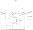
- FIG. 2 is a block diagram illustrating a configuration of the liquid crystal display device according to the first embodiment.
- the circuit board 10 includes an input terminal IN (connector), a DC / DC converter 20 (voltage conversion unit), a voltage dividing circuit 30 (reference resistor), a timing controller 40, and an output terminal. OUT is provided.
- the input terminal IN is supplied with a predetermined input voltage Vin from an external power source.
- the input voltage Vin is, for example, 3.3V.
- the timing controller 40 supplies each circuit with a reference signal for operating each circuit in synchronism based on a horizontal synchronization signal and a vertical synchronization signal input from a control unit (not shown). Specifically, a gate start pulse signal and a gate clock signal are supplied to the gate driver 52 based on the vertical synchronization signal. Based on the horizontal synchronizing signal, the source driver 53 is supplied with a source start pulse signal, a source latch strobe signal, a source clock signal, and a video signal corresponding to the input image.
- the timing controller 40 supplies an output control signal for controlling on / off of the operation of the DC / DC converter 20 to the DC / DC converter 20 to control on / off of the operation of the source driver 53.
- An operation control signal is supplied to the source driver 53, and a switch control signal for controlling ON / OFF of the FET 34 is supplied to the gate terminal of the FET 34.
- the DC / DC converter 20 converts the input voltage Vin supplied from the outside through the input terminal IN into an output voltage Vout having a different voltage value, and outputs the output voltage Vout.
- the output voltage Vout of the DC / DC converter 20 is supplied to the gate driver 52 and the source driver 53 via the output terminal OUT.
- the DC / DC converter 20 includes an operation control FET 21 and switches the output on and off according to the ON / OFF of the operation control FET 21.
- the voltage dividing circuit 30 includes a resistor 31 as an input-side resistor, and a resistor 32 (first resistor) and a resistor 33 (second resistor) connected in parallel as a ground-side resistor.
- an FET 34 is provided between the resistor 32 and the ground.
- the FET 34 has a gate terminal connected to the timing controller 40, a source terminal grounded, and a drain terminal connected to the resistor 32.
- the voltage dividing circuit 30 can change the resistance value of the ground-side resistance unit by controlling ON / OFF of the FET 34, and as a result, changes the output voltage (middle point potential) of the voltage dividing circuit 30. be able to.
- the voltage dividing circuit 30 receives the output voltage Vout of the DC / DC converter 20, and outputs a voltage corresponding to the resistance value of the input-side resistance unit and the resistance value of the ground-side resistance unit. The output voltage of the voltage dividing circuit 30 is supplied to the DC / DC converter 20.
- the DC / DC converter 20 refers to the output voltage of the voltage dividing circuit 30 as the reference voltage Vref, and feedback-controls the output voltage Vout so that the reference voltage Vref becomes a constant voltage.
- the timing controller 40 supplies the switch control signal to the gate terminal of the FET 34 and supplies the output control signal to the DC / DC converter 20.
- the present invention is not limited to this.
- the source driver 53 may supply a switch control signal and an output control signal.
- the DC / DC converter 20 of the present embodiment includes a first state in which an input voltage Vin supplied from the outside is converted into a voltage Vs (first output voltage) used for driving a nonvolatile memory, and generation of a gate signal.
- the voltage value of the output voltage Vout can be switched by switching the second state to be converted into the voltage Vg (second output voltage) used in the above. Details will be described below.
- the output voltage Vout in the first state is as follows.
- the resistance value of the resistor 31 is R1
- the resistance value of the resistor 32 is R2
- the resistance value of the resistor 33 is R3.
- Vout (1 + R1 / R3) ⁇ Vref It becomes.
- the DC / DC converter 20 can output the output voltage Vout in the first state and the output voltage Vout in the second state, and can switch and output two different types of voltages. it can.
- FIG. 3 is a table showing the relationship between ON / OFF (open / close) of the FET 32 and the output voltage of the DC / DC converter 20.
- the gate signal can be generated in the gate driver 52 by setting the output voltage Vout in the second state to ⁇ 13 V and supplying it to the gate driver 52.
- FIG. 4 is a block diagram for explaining switching of the output voltage of the DC / DC converter 20.
- Vg, Vs two different output voltages
- Vin a single input voltage Vin using a single DC / DC converter 20.
- the liquid crystal display device 1 can generate two types of output voltages Vout without using a plurality of DC / DC converters, the circuit board 10 can be reduced in size and consumption as compared with the conventional liquid crystal display device. Electricity and cost reduction can be realized.
- FIG. 5 is a circuit diagram showing a configuration of a voltage dividing circuit according to a modification.
- the voltage dividing circuit 30A includes a resistor 31 and a resistor 32 connected in parallel to each other as an input-side resistor, and a resistor 33 as a ground-side resistor. As described above, the voltage dividing circuit may be configured to change the resistance value of the input-side resistance unit.
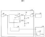
- FIG. 6 is a block diagram showing the configuration of the liquid crystal display device of the second embodiment.
- the source driver 153 in addition to the DC / DC converter 20 (first voltage conversion unit), the source driver 153 includes a DC / DC converter 154 (second voltage conversion unit).
- the DC / DC converter 20 converts the input voltage Vin into a voltage Vg (second output voltage) used for generating the gate signal, and the DC / DC converter 154 uses the input voltage Vin for driving the nonvolatile memory.
- Voltage Vs first output voltage
- the voltage Vg is ⁇ 13V and the voltage Vs is ⁇ 9V.
- the DC / DC converter 154 does not need to be provided inside the source driver 153, and may be provided outside the source driver 153.
- the DC / DC converter 20 is controlled to be turned on and off by an output control signal from the timing controller 40, and can be shut down with high impedance.
- the source driver 153 and the DC / DC converter 154 are controlled to be turned on and off by an operation control signal from the timing controller 40.
- the output of the DC / DC converter 20 is input to a voltage dividing circuit 130 including a resistor 131 and a resistor 132, and the output of the voltage dividing circuit is input to the DC / DC converter 20 as a reference voltage Vref.
- FIG. 7 is a table showing the relationship between the operation of the two DC / DC converters and the output voltage of the DC / DC converter.
- the liquid crystal display device is controlled by the timing controller 40 by stopping the operation of the DC / DC converter 20 (OFF) and operating the DC / DC converter 154 (ON) when the nonvolatile memory is driven.
- a voltage Vs is generated and supplied to the nonvolatile memory.
- the gate signal is generated (when the liquid crystal panel gate is driven)
- the operation of the DC / DC converter 154 is stopped (OFF) and the DC / DC converter 20 is operated (ON) under the control of the timing controller 40.
- a voltage Vg is generated and supplied to the gate driver 52.
- the liquid crystal display device of the present embodiment switches the operating DC / DC converter of the two DC / DC converters under the control of the timing controller 40.
- the DC / DC converter 20 stops operating during the period in which the DC / DC converter 154 outputs the voltage Vs, and the DC / DC converter 154 operates in the period during which the DC / DC converter 20 outputs the voltage Vg. Stop.
- the liquid crystal display device of this embodiment can output two types of voltages (Vg, Vs).
- FIG. 8 is a schematic diagram of the liquid crystal display device of the third embodiment.
- the liquid crystal display device 201 is supplied with a voltage for driving a nonvolatile memory from an external writing device 270 (external inspection device). Further, the writing device 270 checks whether or not a desired writing is performed in the nonvolatile memory after the writing to the nonvolatile memory or whether or not a correct display is performed on the display unit 51. To do.
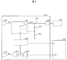
- FIG. 9 is a block diagram illustrating a configuration of the liquid crystal display device according to the third embodiment.
- the circuit board 210 of this embodiment is provided with an input terminal IN1 and an input terminal IN2.
- a predetermined input voltage Vin is supplied from an external power source to the input terminal IN1, and a predetermined input voltage Vcn is supplied from the external writing device 270 to the input terminal IN2.
- the input voltage Vin is, for example, 3.3V.
- the input voltage Vcn is, for example, equal to the voltage Vs for driving the nonvolatile memory, for example, ⁇ 9V.
- the input terminal IN2 is connected to the connector 241A (connection land PIN), and the input voltage Vcn is supplied to the source driver 253 via the connector 241A and the connector 241B.
- the connection between the connector 241A and the connector 241B is controlled by the timing controller 240.
- FIG. 10 is a circuit diagram showing a specific configuration of the connector.
- an FET 241 may be used as the connector 241A and the connector 241B.
- the source terminal of the FET 241 is connected to the input terminal VIN 2, and the drain terminal of the FET 241 is connected to the source driver 253.
- the gate terminal of the FET 241 is connected to the timing controller 240, and ON / OFF of the FET 241 is controlled by the timing controller 240.
- FIG. 11 is a table showing the relationship between the operation of the DC / DC converter, the FET, and the output voltage of the circuit board.
- the liquid crystal display device 201 of the present embodiment stops the operation of the DC / DC converter 20 under the control of the timing controller 240 (OFF), turns the FET 241 on (connected state), and sets the voltage Vs. Is supplied to the nonvolatile memory in the source driver 253.
- the FET 241 is turned off (not connected) and the DC / DC converter 20 is operated (ON) by the control of the timing controller 240, thereby causing the voltage Vg. Is supplied to the gate driver 52.
- the liquid crystal display device 201 of this embodiment switches ON / OFF of the operation of the DC / DC converter 20 and ON / OFF of the FET 241 under the control of the timing controller 240.
- the liquid crystal display device of this embodiment can output two types of voltages (Vg, Vs).
- the nonvolatile memory of the source driver 253 is driven using the input voltage Vcn supplied from the writing device 270 without going through the DC / DC converter. Therefore, a predetermined voltage value ( ⁇ 9V) can be accurately supplied to the nonvolatile memory of the source driver 253. Furthermore, since it is not necessary to drive a plurality of DC / DC converters at the same time, the control of the DC / DC converter is facilitated, and the risk of malfunction or damage can be reduced.
- the DC / DC converter 20 converts the input voltage Vin into the voltage Vg used for generating the gate signal, and supplies the input voltage Vcn to the source driver 253 as the voltage Vs used for driving the nonvolatile memory.
- the DC / DC converter 20 may convert the input voltage Vin into the voltage Vs used for driving the nonvolatile memory, and supply the input voltage Vcn to the gate driver 52 as the voltage Vg used for generating the gate signal.
- N-type FETs or P-type FETs may be used as the FET 34 and the FET 241 depending on the arrangement location.
- the display device includes a scanning line driving circuit (gate driver 52) that generates a gate signal for sequentially selecting pixels, and the above-described image based on an image to be displayed.
- a signal line driver circuit (source driver 53) for generating a data signal to be supplied to the pixel, and the signal line driver circuit is a display device including a nonvolatile memory, and is supplied from the outside.
- a voltage conversion unit (DC / DC converter 20) that converts the voltage (Vin) into an output voltage (Vout) having a different voltage value and outputs the output voltage (Vout), and the voltage conversion unit converts the input voltage into the nonvolatile memory; A first state for converting to a first output voltage (voltage Vs) used for driving, and a second state for converting the input voltage to a second output voltage (voltage Vg) used for generating the gate signal. Wherein the switching between.
- a plurality of DC / DC converters are used even when the first output voltage used for driving the nonvolatile memory is different from the second output voltage used for generating the gate signal.
- the first output voltage and the second output voltage can be generated.
- the display device further includes the voltage dividing circuit (30, 30A) in aspect 1, and the voltage dividing circuit includes an input-side resistance unit and a ground-side resistance unit as resistors.
- the output voltage is input to the voltage dividing circuit, the output of the voltage dividing circuit is input to the voltage conversion unit as a reference voltage (Vref), and the resistance value of the input side resistance unit or the ground side resistance unit
- Vref reference voltage
- the voltage converter may be switched between the first state and the second state based on the reference voltage.
- the output voltage of the voltage converter can be controlled with a simple configuration by referring to the output voltage of the voltage dividing circuit.
- the ground-side resistor unit includes a first resistor (32) and a second resistor (33) connected in parallel, and the first resistor May be configured to be grounded via a switch element (FET 34) and to change the resistance value of the ground-side resistance unit by controlling opening and closing of the switch element.
- FET 34 switch element
- the output voltage of the voltage dividing circuit can be switched by changing the resistance value of the voltage dividing circuit using the switch element.
- the output voltage of the voltage converter can be switched with reference to the output voltage of the voltage dividing circuit.
- the display device generates a scanning line driving circuit (52) that generates a gate signal for sequentially selecting pixels, and generates a data signal to be supplied to the pixel based on an image to be displayed.
- a signal line driving circuit (153) for performing display wherein the signal line driving circuit includes a nonvolatile memory, and an input voltage (Vin) supplied from the outside is applied to the nonvolatile memory.
- a first voltage converter (DC / DC converter 154) that converts and outputs the first output voltage (Vs) used for driving the output, and a second output voltage (Vg) used to generate the gate signal.
- a second voltage converter (DC / DC converter 20) that outputs the first output voltage during the period in which the first voltage converter outputs the first output voltage. Stop operation And, the second voltage converter is in a period for outputting the second output voltage, the first voltage converter is characterized by stopping the operation.
- the input voltage can be converted into two kinds of voltages using the first voltage converter and the second voltage converter. Further, since the first voltage conversion unit and the second voltage conversion unit are not driven at the same time, the voltage conversion unit can be easily controlled, and the risk of malfunction or damage can be reduced.
- the display device includes a scanning line driving circuit (gate driver 52) that generates a gate signal for sequentially selecting pixels, and the above-described image based on an image to be displayed.
- a signal line driver circuit (source driver 253) for generating a data signal to be supplied to the pixel, and the signal line driver circuit is a display device including a nonvolatile memory, An input voltage (Vin) supplied from the outside is converted, and the first output voltage (Vs) used for driving the nonvolatile memory and the second output voltage (Vg) used for generating the gate signal are converted.
- a voltage converter DC / DC converter 20 that outputs one of the voltages as an output voltage
- An input terminal IN2 to which a second input voltage (Vcn) equal to the voltage value of the other of the first output voltage and the second output voltage is supplied from the outside
- a switching element FET 241 for controlling a connection state between the input terminal and the scanning line driving circuit or the nonvolatile memory; The switch element is in a disconnected state during a period in which the voltage converter outputs the output voltage, and the switch element is in a connected state in a period in which the voltage converter does not output the output voltage.
- the nonvolatile memory can be driven and the gate signal can be generated based on the two input voltages.
- a second input voltage equal to the voltage value of the other one of the first output voltage and the second output voltage is supplied from the outside, writing or writing into the nonvolatile memory without going through the DC / DC converter A gate signal can be generated. Therefore, a predetermined voltage value ( ⁇ 9 V) can be accurately supplied to the nonvolatile memory of the source driver.
- a predetermined voltage value ⁇ 9 V
- the present invention can be suitably used for an active matrix drive type display device.
- 1,201 Liquid crystal display device 20 DC / DC converter (voltage converter, first voltage converter) 30, 30A voltage divider circuit 31 Resistance (input side resistance part) 32 resistor (ground side resistor, first resistor) 33 Resistor (Ground-side resistor, 2nd resistor) 52 Gate driver (scanning line drive circuit) 53, 153, 253 Source driver (signal line drive circuit) 154 DC / DC converter (second voltage converter) 34 FET (switch element) Vin input voltage Vcn input voltage Vout output voltage Vref reference voltage IN2 input terminal Vs voltage (first output voltage) Vg voltage (second output voltage)
Landscapes
- Engineering & Computer Science (AREA)
- Physics & Mathematics (AREA)
- Computer Hardware Design (AREA)
- General Physics & Mathematics (AREA)
- Theoretical Computer Science (AREA)
- Chemical & Material Sciences (AREA)
- Crystallography & Structural Chemistry (AREA)
- Control Of Indicators Other Than Cathode Ray Tubes (AREA)
- Liquid Crystal Display Device Control (AREA)
Abstract
簡易な構成を用いて、ゲート信号の生成に用いられる電圧および不揮発性メモリの駆動に用いられる電圧を正確に供給することができる表示装置を提供する。DC/DCコンバータ20は、入力電圧(Vin)を、不揮発性メモリの駆動に用いられる電圧(Vs)に変換する第1の状態と、ゲート信号の生成に用いられる電圧(Vg)に変換する第2の状態とで切り替わる。
Description
本発明は表示装置に関する。
アクティブマトリクス駆動方式の液晶表示装置において、各画素に設けられたTFTのオンおよびオフを制御するために、TFTのゲート端子には、ゲートラインを介して所定のハイ電圧VGHおよびロー電圧VGLの2値の値からなるゲート電圧Vgが供給される。ハイ電圧VGHおよびロー電圧VGLは、液晶表示装置の駆動回路において、外部から入力される入力電圧Vin(例えば3.3V)を元に、DC/DCコンバータによって生成される。
また、ソースドライバは、ソースドライバが備える不揮発性メモリを駆動するための電圧として、ハイ電圧およびロー電圧の2値の値からなる書込み電圧を生成する。
ゲート電圧Vgに要求される電圧値(VGH/VGL)は、TFT特性と液晶セルの電気特性により規定され、書込み電圧に要求される電圧値は、不揮発性メモリの電荷保持特性により規定される。
そのため、ゲート電圧Vgおよび書込み電圧に要求される電圧値は互いに異なり、単一のDC/DCコンバータを用いて生成したハイ電圧およびロー電圧から、ゲート電圧Vgおよび書込み電圧を生成することは好ましくない。
異なる2種類の電圧を供給するための一つの方法として、図12に示すように、ゲート電圧用のハイ電圧およびロー電圧を生成するDC/DCコンバータと、書込み電圧用のハイ電圧およびロー電圧を生成するDC/DCコンバータとをそれぞれ用いることが考えられる。
また、特許文献1~3には、2種類の入力電源に基づいて、回路内部で必要な所定レベルの電源電圧を生成する内部電源制御回路を備えた駆動回路が記載されている。特許文献3の表示装置の駆動回路は、スイッチを介して12Vの電源および40Vの電源に接続されたレベルシフタ回路を備えており、レベルシフタ回路は、ゲートドライバ駆動回路と不揮発性メモリ駆動回路との間で共有されている。これにより、レベルシフタ回路の数を減らし、駆動回路の面積を縮小することができる。
しかしながら、ゲート電圧および書込み電圧を生成するために2つのDC/DCコンバータを用いた場合、高コスト化および高消費電力化を招くため好ましくない。また、2つのDC/DCコンバータを並行して同時に駆動制御した場合、異なる出力電圧が同一の配線上に印加されるため、DC/DCコンバータの制御が困難になり、誤作動を生じたり、破損したりする。
特許文献3の表示装置は、2つの入力電源を必要とする。また、1つのレベルシフタ回路に2種類の電源電圧が入力されるため、レベルシフタ回路において正確な出力制御をすることが困難となる。
本発明は、上記の解題に鑑みなされたものであって、簡易な構成を用いて、ゲート信号の生成に用いられる電圧および不揮発性メモリの駆動に用いられる電圧を正確に供給することができる表示装置を提供することにある。
上記の課題を解決するために、本発明の一態様に係る表示装置は、画素を順次選択状態とするためのゲート信号を生成する走査線駆動回路と、表示すべき映像に基づいて上記画素に供給するデータ信号を生成する信号線駆動回路と、を備えており、上記信号線駆動回路は不揮発性メモリを備えている表示装置であって、外部から供給される入力電圧を異なる電圧値の出力電圧に変換して出力する電圧変換部を備えており、上記電圧変換部は、上記入力電圧を上記不揮発性メモリの駆動に用いられる第1出力電圧に変換する第1の状態と、上記入力電圧を上記ゲート信号の生成に用いられる第2出力電圧に変換する第2の状態とで切り替わることを特徴とする。
また、上記の課題を解決するために、本発明の一態様に係る表示装置は、画素を順次選択状態とするためのゲート信号を生成する走査線駆動回路と、表示すべき映像に基づいて上記画素に供給するデータ信号を生成する信号線駆動回路と、を備えており、上記信号線駆動回路は不揮発性メモリを備えている表示装置であって、外部から供給される入力電圧を、上記不揮発性メモリの駆動に用いられる第1出力電圧に変換して出力する第1電圧変換部と、当該入力電圧を上記ゲート信号の生成に用いられる第2出力電圧に変換して出力する第2電圧変換部とを備えており、上記第1電圧変換部が上記第1出力電圧を出力する期間では、上記第2電圧変換部は動作を停止し、上記第2電圧変換部が上記第2出力電圧を出力する期間では、上記第1電圧変換部は動作を停止することを特徴とする。
また、上記の課題を解決するために、本発明の一態様に係る表示装置は、画素を順次選択状態とするためのゲート信号を生成する走査線駆動回路と、表示すべき映像に基づいて上記画素に供給するデータ信号を生成する信号線駆動回路と、を備えており、上記信号線駆動回路は不揮発性メモリを備えている表示装置であって、外部から供給される入力電圧を変換して、上記不揮発性メモリの駆動に用いられる第1出力電圧および上記ゲート信号の生成に用いられる第2出力電圧のうちの何れか一方の電圧を出力電圧として出力する電圧変換部と、外部から、第1出力電圧および第2出力電圧のうちの何れか他方の電圧値に等しい第2入力電圧が供給される入力端子と、上記入力端子と、上記走査線駆動回路または上記不揮発性メモリとの接続状態を制御するスイッチ素子と、を備えており、上記電圧変換部が上記出力電圧を出力する期間では、上記スイッチ素子は非接続状態となり、上記電圧変換部が上記出力電圧を出力しない期間では、上記スイッチ素子は接続状態となることを特徴とする。
本発明の一態様によれば、簡易な構成を用いて正確な表示制御をすることができる表示装置を提供することができる。
〔実施形態1〕
以下、本発明の実施の形態について、図1~5に基づいて詳細に説明する。以下では、本発明を適用した表示装置の一例として液晶表示装置を挙げて説明するが、本発明はアクティブマトリクス駆動方式の他の表示装置、例えば有機EL表示装置などにも適用することができる。
以下、本発明の実施の形態について、図1~5に基づいて詳細に説明する。以下では、本発明を適用した表示装置の一例として液晶表示装置を挙げて説明するが、本発明はアクティブマトリクス駆動方式の他の表示装置、例えば有機EL表示装置などにも適用することができる。
図1は、実施形態1の液晶表示装置の概略図である。液晶表示装置1は、液晶パネル50と、回路基板10とを備えている。回路基板10と液晶パネル50とは、接続用フレキ60を介して接続されている。
<液晶パネル>
液晶パネル50は、表示部51と、ゲートドライバ52(走査線駆動回路)と、ソースドライバ53(信号線駆動回路)とを備えている。
液晶パネル50は、表示部51と、ゲートドライバ52(走査線駆動回路)と、ソースドライバ53(信号線駆動回路)とを備えている。
表示部51には、図中横方向に延びる複数の走査信号線(不図示)と、図中縦方向に延びる複数のデータ信号線(不図示)とが配されている。走査信号線の一端はゲートドライバ52に接続されており、データ信号線の一端はソースドライバ53に接続されている。
また、表示部51には、走査信号線とデータ信号線とによって囲まれた領域である画素が複数形成されている。表示部51には、各画素に対応して、TFT(スイッチ素子)と画素電極とが設けられている。
TFTのゲート端子は走査信号線に接続されており、ソース端子はデータ信号線に接続されており、ドレイン端子は画素電極に接続されている。
ゲートドライバ52は、回路基板から供給される信号に基づいてゲート信号を生成し、ゲート信号を各走査信号線に供給することによって、各画素を順次選択状態とする。ソースドライバ53は、回路基板から供給される信号に基づいてデータ信号を生成し、データ信号線およびTFTを介して選択状態の画素にデータ信号を書き込む。これにより、表示部51において表示が行われる。
なお、ソースドライバ53には、各種設定を記憶するための不揮発性メモリが搭載されている。
<回路基板>
回路基板10は、外部から供給される映像信号に基づいて、ゲートドライバ52およびソースドライバ53を駆動するための各種信号を生成する。各種信号は、接続用フレキ60を介してゲートドライバ52およびソースドライバ53に供給される。
回路基板10は、外部から供給される映像信号に基づいて、ゲートドライバ52およびソースドライバ53を駆動するための各種信号を生成する。各種信号は、接続用フレキ60を介してゲートドライバ52およびソースドライバ53に供給される。
図2は、実施形態1の液晶表示装置の構成を示すブロック図である。
図2に示すように、回路基板10には、入力端子IN(コネクター)と、DC/DCコンバータ20(電圧変換部)と、分圧回路30(リファレンス抵抗)と、タイミングコントローラ40と、出力端子OUTとが設けられている。
入力端子INには、外部の電源から所定の入力電圧Vinが供給される。入力電圧Vinは、例えば3.3Vである。
タイミングコントローラ40は、図示しないコントロール部から入力された水平同期信号及び垂直同期信号に基づき、各回路が同期して動作するための基準となる信号を各回路に対して供給する。具体的には、ゲートドライバ52には、垂直同期信号に基づいて、ゲートスタートパルス信号およびゲートクロック信号を供給する。ソースドライバ53には、水平同期信号に基づいて、ソーススタートパルス信号、ソースラッチストローブ信号、ソースクロック信号、および入力画像に応じた映像信号を供給する。
さらに、タイミングコントローラ40は、DC/DCコンバータ20の動作のオンおよびオフを制御するための出力制御信号をDC/DCコンバータ20に供給し、ソースドライバ53の動作のオンおよびオフを制御するための動作制御信号をソースドライバ53に供給し、FET34のON/OFFを制御するためのスイッチ制御信号をFET34のゲート端子に供給する。
DC/DCコンバータ20は、入力端子INを介して外部から供給される入力電圧Vinを、異なる電圧値の出力電圧Voutに変換して出力する。DC/DCコンバータ20の出力電圧Voutは、出力端子OUTを介して、ゲートドライバ52およびソースドライバ53に供給される。DC/DCコンバータ20は、動作制御用FET21を備えており、動作制御用FET21のON/OFFに応じて出力のオンおよびオフを切り替える。
分圧回路30は、入力側抵抗部としての抵抗31と、グランド側抵抗部として互いに並列接続された抵抗32(第1抵抗)および抵抗33(第2抵抗)と、を備えている。
また、抵抗32とグランドとの間には、FET34が設けられている。FET34は、ゲート端子がタイミングコントローラ40に接続されており、ソース端子が接地されており、ドレイン端子が抵抗32に接続されている。分圧回路30は、FET34のON/OFFを制御することによって、グランド側抵抗部の抵抗値を変化させることができ、その結果、分圧回路30の出力電圧(中点の電位)を変化させることができる。
分圧回路30は、DC/DCコンバータ20の出力電圧Voutが入力され、入力側抵抗部の抵抗値とグランド側抵抗部の抵抗値に応じた電圧を出力する。分圧回路30の出力電圧は、DC/DCコンバータ20に供給される。
DC/DCコンバータ20は、分圧回路30の出力電圧を参照電圧Vrefとして参照し、参照電圧Vrefが一定の電圧となるよう、出力電圧Voutをフィードバック制御する。
なお、上記の説明では、タイミングコントローラ40が、FET34のゲート端子にスイッチ制御信号を供給し、DC/DCコンバータ20に出力制御信号を供給する構成について説明したが、これに限られない。タイミングコントローラ40に代えてソースドライバ53が、スイッチ制御信号および出力制御信号を供給する構成であってもよい。
<出力電圧Vout>
本実施形態のDC/DCコンバータ20は、外部から供給される入力電圧Vinを、不揮発性メモリの駆動に用いられる電圧Vs(第1出力電圧)に変換する第1の状態と、ゲート信号の生成に用いられる電圧Vg(第2出力電圧)に変換する第2の状態とを切り替えることによって、出力電圧Voutの電圧値を切り替えることができる。以下、詳細に説明する。
本実施形態のDC/DCコンバータ20は、外部から供給される入力電圧Vinを、不揮発性メモリの駆動に用いられる電圧Vs(第1出力電圧)に変換する第1の状態と、ゲート信号の生成に用いられる電圧Vg(第2出力電圧)に変換する第2の状態とを切り替えることによって、出力電圧Voutの電圧値を切り替えることができる。以下、詳細に説明する。
第1の状態では、タイミングコントローラ40からFET34のゲート端子にロー電位の信号が供給され、FET34はオフ状態となる。上述したように、DC/DCコンバータ20は、参照電圧Vrefが一定の電圧となるよう、出力電圧Voutをフィードバック制御する。そのため、第1の状態における出力電圧Voutは、抵抗31の抵抗値をR1、抵抗32の抵抗値をR2、抵抗33の抵抗値をR3とすると、
Vout=(1+R1/R3)×Vref
となる。
Vout=(1+R1/R3)×Vref
となる。
一方、第2の状態では、タイミングコントローラ40からFET34のゲート端子にハイ電位の信号が供給され、FET34はオン状態となる。そのため、第1の状態における出力電圧Voutは、R2とR3の合成抵抗(R2//R3)をR23とすると、
Vout=(1+R1/R23)×Vref
となる。
Vout=(1+R1/R23)×Vref
となる。
以上のように、DC/DCコンバータ20は、第1の状態における出力電圧Voutと、第2の状態における出力電圧Voutとを出力することができ、異なる2種類の電圧を切り替えて出力することができる。
図3は、FET32のON/OFF(開閉)と、DC/DCコンバータ20の出力電圧の関係を示す表である。
図3に示すように、例えば、第1の状態における出力電圧Voutを±9Vに設定し、ソースドライバ53に供給することによって、ソースドライバ53の内部の不揮発性メモリを駆動し、不揮発性メモリへのデータ書込みおよびデータ消去をすることができる。また、第2の状態における出力電圧Voutを±13Vに設定し、ゲートドライバ52に供給することによって、ゲートドライバ52においてゲート信号を生成することができる。
図4は、DC/DCコンバータ20の出力電圧の切り替えを説明するためのブロック図である。図4に示すように、本実施形態の液晶表示装置1によれば、単一のDC/DCコンバータ20を用いて、単一の入力電圧Vinから、異なる2種類の出力電圧Vout(Vg、Vs)を生成し、ゲートドライバ52およびソースドライバ53に供給することができる。
そのため、液晶表示装置1は、複数のDC/DCコンバータを用いることなく2種類の出力電圧Voutを生成することができるため、従来の液晶表示装置に比べて、回路基板10の小型化および低消費電力化、さらに低コスト化を実現することができる。
<変形例>
なお、分圧回路30の回路構成は、図2に示す構成に限られない。図5は、変形例に係る分圧回路の構成を示す回路図である。
なお、分圧回路30の回路構成は、図2に示す構成に限られない。図5は、変形例に係る分圧回路の構成を示す回路図である。
変形例に係る分圧回路30Aは、入力側抵抗部として互いに並列に接続された抵抗31および抵抗32と、グランド側抵抗部としての抵抗33と、を備えている。このように、分圧回路は、入力側抵抗部の抵抗値を変化させることができる構成であってもよい。
〔実施形態2〕
本発明の他の実施形態について、図6~図7に基づいて説明すれば、以下のとおりである。なお、説明の便宜上、前記実施形態にて説明した部材と同じ機能を有する部材については、同じ符号を付記し、その説明を省略する。
本発明の他の実施形態について、図6~図7に基づいて説明すれば、以下のとおりである。なお、説明の便宜上、前記実施形態にて説明した部材と同じ機能を有する部材については、同じ符号を付記し、その説明を省略する。
図6は、実施形態2の液晶表示装置の構成を示すブロック図である。
本実施形態の液晶表示装置は、DC/DCコンバータ20(第1電圧変換部)に加えて、ソースドライバ153にDC/DCコンバータ154(第2電圧変換部)が搭載されている。
DC/DCコンバータ20は、入力電圧Vinを、ゲート信号の生成に用いられる電圧Vg(第2出力電圧)に変換し、DC/DCコンバータ154は、入力電圧Vinを、不揮発性メモリの駆動に用いられる電圧Vs(第1出力電圧)に変換する。例えば、電圧Vgは±13Vであり、電圧Vsは±9Vである。なお、DC/DCコンバータ154は、ソースドライバ153の内部に設けられている必要はなく、ソースドライバ153の外部に設けられていてもよい。
DC/DCコンバータ20は、タイミングコントローラ40からの出力制御信号により、動作のオンおよびオフを制御され、ハイインピーダンスでシャットダウンをすることができる。ソースドライバ153およびDC/DCコンバータ154は、タイミングコントローラ40からの動作制御信号により、動作のオンおよびオフを制御される。
また、DC/DCコンバータ20の出力は、抵抗131および抵抗132からなる分圧回路130に入力され、分圧回路の出力は参照電圧VrefとしてDC/DCコンバータ20に入力される。
図7は、2つのDC/DCコンバータの動作と、DC/DCコンバータの出力電圧の関係を示す表である。
本実施形態の液晶表示装置は、タイミングコントローラ40の制御により、不揮発性メモリの駆動時には、DC/DCコンバータ20の動作を停止し(OFF)、DC/DCコンバータ154を動作させる(ON)ことによって電圧Vsを生成し、不揮発性メモリに供給する。一方で、ゲート信号生成時時(液晶パネルゲート駆動時)には、タイミングコントローラ40の制御により、DC/DCコンバータ154の動作を停止し(OFF)、DC/DCコンバータ20を動作させる(ON)ことによって電圧Vgを生成し、ゲートドライバ52に供給する。
すなわち、本実施形態の液晶表示装置は、タイミングコントローラ40の制御により、2つのDC/DCコンバータのうちの動作するDC/DCコンバータを切り替える。
これにより、DC/DCコンバータ154が電圧Vsを出力する期間では、DC/DCコンバータ20は動作を停止し、DC/DCコンバータ20が電圧Vgを出力する期間では、DC/DCコンバータ154は動作を停止する。
以上の構成によれば、本実施形態の液晶表示装置は、2種類の電圧(Vg、Vs)を出力することができる。
なお、複数のソースドライバ153に内蔵された不揮発性メモリには、データを1つ1つ時系列で書き込むことができるため、複数のDC/DCコンバータを同時に駆動する必要はない。そのため、DC/DCコンバータの制御が容易になり、誤作動を生じたり、破損したりする危険性を低減することができる。
〔実施形態3〕
本発明の他の実施形態について、図8~図10に基づいて説明すれば、以下のとおりである。なお、説明の便宜上、前記実施形態にて説明した部材と同じ機能を有する部材については、同じ符号を付記し、その説明を省略する。
本発明の他の実施形態について、図8~図10に基づいて説明すれば、以下のとおりである。なお、説明の便宜上、前記実施形態にて説明した部材と同じ機能を有する部材については、同じ符号を付記し、その説明を省略する。
図8は、実施形態3の液晶表示装置の概略図である。
液晶表示装置201は、外部の書込み装置270(外部検査装置)から不揮発性メモリを駆動するための電圧を供給される。さらに、書込み装置270は、不揮発性メモリへの書込みが行われたあとに、不揮発性メモリに所望の書込みが行なわれたかどうか、あるいは表示部51において正しい表示が行われているかどうか、などを検査する。
図9は、実施形態3の液晶表示装置の構成を示すブロック図である。
本実施形態の回路基板210には、入力端子IN1と、入力端子IN2とが設けられている。
入力端子IN1には、外部の電源から所定の入力電圧Vinが供給され、入力端子IN2には、外部の書込み装置270から所定の入力電圧Vcnが供給される。入力電圧Vinは、例えば3.3Vである。入力電圧Vcnは、例えば、不揮発性メモリを駆動するための電圧Vsと等しく、例えば±9Vである。
入力端子IN2は、コネクタ241A(接続ランドPIN)に接続されており、入力電圧Vcnはコネクタ241Aおよびコネクタ241Bを介してソースドライバ253に供給される。コネクタ241Aとコネクタ241Bとの接続は、タイミングコントローラ240によって制御される。
図10は、コネクタの具体的構成を示す回路図である。図10に示すように、コネクタ241Aおよびコネクタ241Bとして、FET241を用いてもよい。FET241のソース端子は入力端子VIN2に接続されており、FET241のドレイン端子はソースドライバ253に接続されている。FET241のゲート端子はタイミングコントローラ240に接続されており、FET241のON/OFFはタイミングコントローラ240によって制御される。
図11は、DC/DCコンバータの動作およびFETと、回路基板の出力電圧の関係を示す表である。
本実施形態の液晶表示装置201は、不揮発性メモリの駆動時には、タイミングコントローラ240の制御により、DC/DCコンバータ20の動作を停止し(OFF)、FET241をON状態(接続状態)とし、電圧Vsをソースドライバ253内の不揮発性メモリに供給する。一方で、ゲート信号生成時(液晶パネルゲート駆動時)には、タイミングコントローラ240の制御により、FET241をOFF状態(非接続状態)とし、DC/DCコンバータ20を動作させる(ON)ことによって電圧Vgを生成し、ゲートドライバ52に供給する。
すなわち、本実施形態の液晶表示装置201は、タイミングコントローラ240の制御により、DC/DCコンバータ20の動作のON/OFFと、FET241のON/OFFとを切り替える。
以上の構成によれば、本実施形態の液晶表示装置は、2種類の電圧(Vg、Vs)を出力することができる。
また、本実施形態の液晶表示装置において、ソースドライバ253の不揮発性メモリの駆動は、DC/DCコンバータを介することなく、書込み装置270から供給される入力電圧Vcnを用いて行われる。そのため、所定の電圧値(±9V)を正確にソースドライバ253の不揮発性メモリに供給することができる。さらに、複数のDC/DCコンバータを同時に駆動する必要がないため、DC/DCコンバータの制御が容易になり、誤作動を生じたり、破損したりする危険性を低減することができる。
なお、上記の説明では、DC/DCコンバータ20が入力電圧Vinをゲート信号の生成に用いられる電圧Vgに変換し、入力電圧Vcnを不揮発性メモリの駆動に用いられる電圧Vsとしてソースドライバ253に供給する例について説明したが、これに限られない。
すなわち、DC/DCコンバータ20が入力電圧Vinを不揮発性メモリの駆動に用いられる電圧Vsに変換し、入力電圧Vcnをゲート信号の生成に用いられる電圧Vgとしてゲートドライバ52に供給してもよい。
なお、上記の説明において、FET34およびFET241としては、配置箇所に応じて、N型FETを用いてもよいし、P型FETを用いてもよい。
〔まとめ〕
本発明の態様1に係る表示装置(液晶表示装置1)は、画素を順次選択状態とするためのゲート信号を生成する走査線駆動回路(ゲートドライバ52)と、表示すべき映像に基づいて上記画素に供給するデータ信号を生成する信号線駆動回路(ソースドライバ53)と、を備えており、上記信号線駆動回路は不揮発性メモリを備えている表示装置であって、外部から供給される入力電圧(Vin)を異なる電圧値の出力電圧(Vout)に変換して出力する電圧変換部(DC/DCコンバータ20)を備えており、上記電圧変換部は、上記入力電圧を上記不揮発性メモリの駆動に用いられる第1出力電圧(電圧Vs)に変換する第1の状態と、上記入力電圧を上記ゲート信号の生成に用いられる第2出力電圧(電圧Vg)に変換する第2の状態とで切り替わることを特徴とする。
本発明の態様1に係る表示装置(液晶表示装置1)は、画素を順次選択状態とするためのゲート信号を生成する走査線駆動回路(ゲートドライバ52)と、表示すべき映像に基づいて上記画素に供給するデータ信号を生成する信号線駆動回路(ソースドライバ53)と、を備えており、上記信号線駆動回路は不揮発性メモリを備えている表示装置であって、外部から供給される入力電圧(Vin)を異なる電圧値の出力電圧(Vout)に変換して出力する電圧変換部(DC/DCコンバータ20)を備えており、上記電圧変換部は、上記入力電圧を上記不揮発性メモリの駆動に用いられる第1出力電圧(電圧Vs)に変換する第1の状態と、上記入力電圧を上記ゲート信号の生成に用いられる第2出力電圧(電圧Vg)に変換する第2の状態とで切り替わることを特徴とする。
上記の構成によれば、不揮発性メモリの駆動に用いられる第1出力電圧と、ゲート信号の生成に用いられる第2出力電圧とが異なる場合であっても、複数のDC/DCコンバータを用いることなく、第1出力電圧および第2出力電圧を生成することができる。
これにより、従来の液晶表示装置に比べて、小型化および低消費電力化、さらに低コスト化を実現することができる。
本発明の態様2に係る表示装置は、上記態様1において、分圧回路(30、30A)をさらに備えており、上記分圧回路は、抵抗として、入力側抵抗部およびグランド側抵抗部を備えており、上記出力電圧は上記分圧回路に入力され、上記分圧回路の出力は参照電圧(Vref)として上記電圧変換部に入力され、上記入力側抵抗部または上記グランド側抵抗部の抵抗値を変化させたときに、上記電圧変換部は、上記参照電圧に基づいて、上記第1の状態と上記第2の状態とで切り替わる構成であってもよい。
上記の構成によれば、分圧回路の出力電圧を参照して、簡易な構成により、電圧変換部の出力電圧を制御することができる。
本発明の態様3に係る表示装置は、上記態様2において、上記グランド側抵抗部は、並列接続された第1抵抗(32)および第2抵抗(33)を有しており、上記第1抵抗は、スイッチ素子(FET34)を介して接地されており、上記スイッチ素子の開閉を制御することによって、上記グランド側抵抗部の抵抗値を変化させる構成であってもよい。
上記の構成によれば、スイッチ素子を用いて分圧回路の抵抗値を変化させることによって、分圧回路の出力電圧を切り替えることができる。これにより、分圧回路の出力電圧を参照して電圧変換部の出力電圧を切り替えることができる。
本発明の態様4に係る表示装置は、画素を順次選択状態とするためのゲート信号を生成する走査線駆動回路(52)と、表示すべき映像に基づいて上記画素に供給するデータ信号を生成する信号線駆動回路(153)と、を備えており、上記信号線駆動回路は不揮発性メモリを備えている表示装置であって、外部から供給される入力電圧(Vin)を、上記不揮発性メモリの駆動に用いられる第1出力電圧(Vs)に変換して出力する第1電圧変換部(DC/DCコンバータ154)と、当該入力電圧を上記ゲート信号の生成に用いられる第2出力電圧(Vg)に変換して出力する第2電圧変換部(DC/DCコンバータ20)とを備えており、上記第1電圧変換部が上記第1出力電圧を出力する期間では、上記第2電圧変換部は動作を停止し、上記第2電圧変換部が上記第2出力電圧を出力する期間では、上記第1電圧変換部は動作を停止することを特徴とする。
上記の構成によれば、入力電圧を、第1電圧変換部および第2電圧変換部を用いて、2種類の電圧に変換することができる。また、第1電圧変換部および第2電圧変換部は、同時に駆動されないため、電圧変換部の制御が容易になり、誤作動を生じたり、破損したりする危険性を低減することができる。
本発明の態様5に係る表示装置(液晶表示装置201)は、画素を順次選択状態とするためのゲート信号を生成する走査線駆動回路(ゲートドライバ52)と、表示すべき映像に基づいて上記画素に供給するデータ信号を生成する信号線駆動回路(ソースドライバ253)と、を備えており、上記信号線駆動回路は不揮発性メモリを備えている表示装置であって、
外部から供給される入力電圧(Vin)を変換して、上記不揮発性メモリの駆動に用いられる第1出力電圧(Vs)および上記ゲート信号の生成に用いられる第2出力電圧(Vg)のうちの何れか一方の電圧を出力電圧として出力する電圧変換部(DC/DCコンバータ20)と、
外部から、第1出力電圧および第2出力電圧のうちの何れか他方の電圧値に等しい第2入力電圧(Vcn)が供給される入力端子(IN2)と、
上記入力端子と、上記走査線駆動回路または上記不揮発性メモリとの接続状態を制御するスイッチ素子(FET241)と、を備えており、
上記電圧変換部が上記出力電圧を出力する期間では、上記スイッチ素子は非接続状態となり、上記電圧変換部が上記出力電圧を出力しない期間では、上記スイッチ素子は接続状態となることを特徴とする。
外部から供給される入力電圧(Vin)を変換して、上記不揮発性メモリの駆動に用いられる第1出力電圧(Vs)および上記ゲート信号の生成に用いられる第2出力電圧(Vg)のうちの何れか一方の電圧を出力電圧として出力する電圧変換部(DC/DCコンバータ20)と、
外部から、第1出力電圧および第2出力電圧のうちの何れか他方の電圧値に等しい第2入力電圧(Vcn)が供給される入力端子(IN2)と、
上記入力端子と、上記走査線駆動回路または上記不揮発性メモリとの接続状態を制御するスイッチ素子(FET241)と、を備えており、
上記電圧変換部が上記出力電圧を出力する期間では、上記スイッチ素子は非接続状態となり、上記電圧変換部が上記出力電圧を出力しない期間では、上記スイッチ素子は接続状態となることを特徴とする。
上記の構成によれば、2つの入力電圧に基づいて、不揮発性メモリを駆動し、ゲート信号を生成することができる。また、外部から、第1出力電圧および第2出力電圧のうちの何れか他方の電圧値に等しい第2入力電圧が供給されるため、DC/DCコンバータを介することなく、不揮発性メモリの書込みまたはゲート信号の生成を行うことができる。そのため、所定の電圧値(±9V)を正確にソースドライバの不揮発性メモリに供給することができる。さらに、複数のDC/DCコンバータを同時に駆動する必要がないため、DC/DCコンバータの制御が容易になり、誤作動を生じたり、破損したりする危険性を低減することができる。
本発明は上述した各実施形態に限定されるものではなく、請求項に示した範囲で種々の変更が可能であり、異なる実施形態にそれぞれ開示された技術的手段を適宜組み合わせて得られる実施形態についても本発明の技術的範囲に含まれる。さらに、各実施形態にそれぞれ開示された技術的手段を組み合わせることにより、新しい技術的特徴を形成することができる。
本発明は、アクティブマトリクス駆動方式の表示装置に好適に利用することができる。
1、201 液晶表示装置(表示装置)
20 DC/DCコンバータ(電圧変換部、第1電圧変換部)
30、30A 分圧回路
31 抵抗(入力側抵抗部)
32 抵抗(グランド側抵抗部、第1抵抗)
33 抵抗(グランド側抵抗部、第2抵抗)
52 ゲートドライバ(走査線駆動回路)
53、153、253 ソースドライバ(信号線駆動回路)
154 DC/DCコンバータ(第2電圧変換部)
34 FET(スイッチ素子)
Vin 入力電圧
Vcn 入力電圧
Vout 出力電圧
Vref 参照電圧
IN2 入力端子
Vs 電圧(第1出力電圧)
Vg 電圧(第2出力電圧)
20 DC/DCコンバータ(電圧変換部、第1電圧変換部)
30、30A 分圧回路
31 抵抗(入力側抵抗部)
32 抵抗(グランド側抵抗部、第1抵抗)
33 抵抗(グランド側抵抗部、第2抵抗)
52 ゲートドライバ(走査線駆動回路)
53、153、253 ソースドライバ(信号線駆動回路)
154 DC/DCコンバータ(第2電圧変換部)
34 FET(スイッチ素子)
Vin 入力電圧
Vcn 入力電圧
Vout 出力電圧
Vref 参照電圧
IN2 入力端子
Vs 電圧(第1出力電圧)
Vg 電圧(第2出力電圧)
Claims (5)
- 画素を順次選択状態とするためのゲート信号を生成する走査線駆動回路と、表示すべき映像に基づいて上記画素に供給するデータ信号を生成する信号線駆動回路と、を備えており、上記信号線駆動回路は不揮発性メモリを備えている表示装置であって、
外部から供給される入力電圧を異なる電圧値の出力電圧に変換して出力する電圧変換部を備えており、
上記電圧変換部は、上記入力電圧を上記不揮発性メモリの駆動に用いられる第1出力電圧に変換する第1の状態と、上記入力電圧を上記ゲート信号の生成に用いられる第2出力電圧に変換する第2の状態とで切り替わることを特徴とする表示装置。 - 分圧回路をさらに備えており、
上記分圧回路は、抵抗として、入力側抵抗部およびグランド側抵抗部を備えており、
上記出力電圧は上記分圧回路に入力され、上記分圧回路の出力は参照電圧として上記電圧変換部に入力され、
上記入力側抵抗部または上記グランド側抵抗部の抵抗値を変化させたときに、上記電圧変換部は、上記参照電圧に基づいて、上記第1の状態と上記第2の状態とで切り替わることを特徴とする請求項1に記載の表示装置。 - 上記グランド側抵抗部は、並列接続された第1抵抗および第2抵抗を有しており、
上記第1抵抗は、スイッチ素子を介して接地されており、
上記スイッチ素子の開閉を制御することによって、上記グランド側抵抗部の抵抗値を変化させることを特徴とする請求項2に記載の表示装置。 - 画素を順次選択状態とするためのゲート信号を生成する走査線駆動回路と、表示すべき映像に基づいて上記画素に供給するデータ信号を生成する信号線駆動回路と、を備えており、上記信号線駆動回路は不揮発性メモリを備えている表示装置であって、
外部から供給される入力電圧を、上記不揮発性メモリの駆動に用いられる第1出力電圧に変換して出力する第1電圧変換部と、当該入力電圧を上記ゲート信号の生成に用いられる第2出力電圧に変換して出力する第2電圧変換部とを備えており、
上記第1電圧変換部が上記第1出力電圧を出力する期間では、上記第2電圧変換部は動作を停止し、上記第2電圧変換部が上記第2出力電圧を出力する期間では、上記第1電圧変換部は動作を停止することを特徴とする表示装置。 - 画素を順次選択状態とするためのゲート信号を生成する走査線駆動回路と、表示すべき映像に基づいて上記画素に供給するデータ信号を生成する信号線駆動回路と、を備えており、上記信号線駆動回路は不揮発性メモリを備えている表示装置であって、
外部から供給される入力電圧を変換して、上記不揮発性メモリの駆動に用いられる第1出力電圧および上記ゲート信号の生成に用いられる第2出力電圧のうちの何れか一方の電圧を出力電圧として出力する電圧変換部と、
外部から、第1出力電圧および第2出力電圧のうちの何れか他方の電圧値に等しい第2入力電圧が供給される入力端子と、
上記入力端子と、上記走査線駆動回路または上記不揮発性メモリとの接続状態を制御するスイッチ素子と、を備えており、
上記電圧変換部が上記出力電圧を出力する期間では、上記スイッチ素子は非接続状態となり、上記電圧変換部が上記出力電圧を出力しない期間では、上記スイッチ素子は接続状態となることを特徴とする表示装置。
Priority Applications (1)
| Application Number | Priority Date | Filing Date | Title |
|---|---|---|---|
| US15/030,408 US20160260374A1 (en) | 2013-11-05 | 2014-10-16 | Display device |
Applications Claiming Priority (2)
| Application Number | Priority Date | Filing Date | Title |
|---|---|---|---|
| JP2013-229558 | 2013-11-05 | ||
| JP2013229558 | 2013-11-05 |
Publications (1)
| Publication Number | Publication Date |
|---|---|
| WO2015068552A1 true WO2015068552A1 (ja) | 2015-05-14 |
Family
ID=53041335
Family Applications (1)
| Application Number | Title | Priority Date | Filing Date |
|---|---|---|---|
| PCT/JP2014/077588 Ceased WO2015068552A1 (ja) | 2013-11-05 | 2014-10-16 | 表示装置 |
Country Status (2)
| Country | Link |
|---|---|
| US (1) | US20160260374A1 (ja) |
| WO (1) | WO2015068552A1 (ja) |
Families Citing this family (4)
| Publication number | Priority date | Publication date | Assignee | Title |
|---|---|---|---|---|
| JP6702284B2 (ja) * | 2017-09-05 | 2020-06-03 | 株式会社デンソー | 液晶パネルの駆動回路および液晶表示装置 |
| US11705037B1 (en) * | 2020-09-25 | 2023-07-18 | Apple Inc. | Foveated driving for power saving |
| CN112994436B (zh) * | 2021-02-04 | 2022-06-03 | 重庆先进光电显示技术研究院 | 一种栅极开启电压产生电路、显示面板驱动装置及显示装置 |
| CN113160730A (zh) * | 2021-04-07 | 2021-07-23 | Tcl华星光电技术有限公司 | 驱动电路及显示装置 |
Citations (5)
| Publication number | Priority date | Publication date | Assignee | Title |
|---|---|---|---|---|
| JP2001282164A (ja) * | 2000-03-31 | 2001-10-12 | Sanyo Electric Co Ltd | 表示装置用駆動装置 |
| JP2005266311A (ja) * | 2004-03-18 | 2005-09-29 | Seiko Epson Corp | 電源回路、表示ドライバ及び表示装置 |
| JP2007010894A (ja) * | 2005-06-29 | 2007-01-18 | Nec Electronics Corp | 駆動回路及び表示装置 |
| JP2007122766A (ja) * | 2005-10-25 | 2007-05-17 | Seiko Epson Corp | 液晶ドライバ |
| JP2010117506A (ja) * | 2008-11-12 | 2010-05-27 | Seiko Epson Corp | 表示ドライバ及び電気光学装置 |
Family Cites Families (10)
| Publication number | Priority date | Publication date | Assignee | Title |
|---|---|---|---|---|
| JP3105718B2 (ja) * | 1993-11-19 | 2000-11-06 | 日本電気株式会社 | 個別選択呼出受信機 |
| JP3653165B2 (ja) * | 1997-07-09 | 2005-05-25 | アルプス電気株式会社 | 液晶表示装置の駆動電圧発生装置 |
| US8525762B2 (en) * | 2006-11-16 | 2013-09-03 | Innolux Corporation | Systems and methods for adjusting display parameters of an active matrix organic light emitting diode panel |
| TW200849784A (en) * | 2007-06-12 | 2008-12-16 | Vastview Tech Inc | DC-DC converter with temperature compensation circuit |
| KR101509116B1 (ko) * | 2007-11-13 | 2015-04-06 | 삼성디스플레이 주식회사 | 표시 장치와 그 구동 장치 및 구동 방법 |
| KR20100041151A (ko) * | 2008-10-13 | 2010-04-22 | 삼성전자주식회사 | 스위치 회로, dc-dc 컨버터 및 이를 구비하는 디스플레이 구동 장치 |
| KR101056289B1 (ko) * | 2009-02-27 | 2011-08-11 | 삼성모바일디스플레이주식회사 | Dc― dc 컨버터 및 그를 이용한 유기전계발광표시장치 |
| CN102751872B (zh) * | 2011-04-21 | 2016-04-06 | 登丰微电子股份有限公司 | 反馈控制电路 |
| KR101960365B1 (ko) * | 2011-11-22 | 2019-03-21 | 엘지디스플레이 주식회사 | 액정표시장치의 구동회로 |
| US9337731B2 (en) * | 2012-12-13 | 2016-05-10 | Linear Technology Corporation | Power converter for generating both positive and negative output signals |
-
2014
- 2014-10-16 WO PCT/JP2014/077588 patent/WO2015068552A1/ja not_active Ceased
- 2014-10-16 US US15/030,408 patent/US20160260374A1/en not_active Abandoned
Patent Citations (5)
| Publication number | Priority date | Publication date | Assignee | Title |
|---|---|---|---|---|
| JP2001282164A (ja) * | 2000-03-31 | 2001-10-12 | Sanyo Electric Co Ltd | 表示装置用駆動装置 |
| JP2005266311A (ja) * | 2004-03-18 | 2005-09-29 | Seiko Epson Corp | 電源回路、表示ドライバ及び表示装置 |
| JP2007010894A (ja) * | 2005-06-29 | 2007-01-18 | Nec Electronics Corp | 駆動回路及び表示装置 |
| JP2007122766A (ja) * | 2005-10-25 | 2007-05-17 | Seiko Epson Corp | 液晶ドライバ |
| JP2010117506A (ja) * | 2008-11-12 | 2010-05-27 | Seiko Epson Corp | 表示ドライバ及び電気光学装置 |
Also Published As
| Publication number | Publication date |
|---|---|
| US20160260374A1 (en) | 2016-09-08 |
Similar Documents
| Publication | Publication Date | Title |
|---|---|---|
| US7873140B2 (en) | Shift register | |
| US9620240B2 (en) | Shift register | |
| US10229634B2 (en) | Level shifting unit, level shifting circuit, method for driving the level shifting circuit, gate driving circuit and display device | |
| US8041000B2 (en) | Shift register | |
| KR102232915B1 (ko) | 표시 장치 | |
| KR101799981B1 (ko) | 표시 장치 및 그것의 구동 방법 | |
| US20110234565A1 (en) | Shift register circuit, display device, and method for driving shift register circuit | |
| JP4337065B2 (ja) | 液晶表示装置 | |
| US9430982B2 (en) | Display apparatus | |
| CN112309333B (zh) | 有源矩阵基板、显示装置及其驱动方法 | |
| CN112992092A (zh) | 一种驱动电路和驱动电路的控制方法 | |
| US10770022B2 (en) | Source driver and a display driver integrated circuit | |
| US8786353B2 (en) | Multi-channel semiconductor device and display device comprising same | |
| WO2015068552A1 (ja) | 表示装置 | |
| US9934743B2 (en) | Drive device, drive method, display device and display method | |
| CN102479497B (zh) | 液晶显示面板的驱动装置 | |
| KR102023932B1 (ko) | 전원 공급부 및 이를 이용한 평판 표시 장치 | |
| US20110148845A1 (en) | Driving method of a display device and display device | |
| KR20090005500A (ko) | 액정 표시장치의 구동장치와 그 구동방법 | |
| KR102034054B1 (ko) | 전원 공급부 및 이를 이용한 평판 표시 장치 | |
| WO2012090803A1 (ja) | 液晶表示装置 | |
| CN101162335A (zh) | 栅极驱动器、光电装置、电子设备以及驱动方法 | |
| KR20080003199A (ko) | 화상표시장치 및 이의 구동방법 | |
| TWI668680B (zh) | 電泳顯示裝置及電子顯示機器 | |
| US9590620B2 (en) | Gate driving circuit and display panel using the same |
Legal Events
| Date | Code | Title | Description |
|---|---|---|---|
| 121 | Ep: the epo has been informed by wipo that ep was designated in this application |
Ref document number: 14860990 Country of ref document: EP Kind code of ref document: A1 |
|
| WWE | Wipo information: entry into national phase |
Ref document number: 15030408 Country of ref document: US |
|
| NENP | Non-entry into the national phase |
Ref country code: DE |
|
| 122 | Ep: pct application non-entry in european phase |
Ref document number: 14860990 Country of ref document: EP Kind code of ref document: A1 |
|
| NENP | Non-entry into the national phase |
Ref country code: JP |