WO2015064252A1 - 透明液晶表示装置 - Google Patents
透明液晶表示装置 Download PDFInfo
- Publication number
- WO2015064252A1 WO2015064252A1 PCT/JP2014/075485 JP2014075485W WO2015064252A1 WO 2015064252 A1 WO2015064252 A1 WO 2015064252A1 JP 2014075485 W JP2014075485 W JP 2014075485W WO 2015064252 A1 WO2015064252 A1 WO 2015064252A1
- Authority
- WO
- WIPO (PCT)
- Prior art keywords
- liquid crystal
- display device
- crystal panel
- driver
- crystal display
- Prior art date
- Legal status (The legal status is an assumption and is not a legal conclusion. Google has not performed a legal analysis and makes no representation as to the accuracy of the status listed.)
- Ceased
Links
Images





Classifications
-
- G—PHYSICS
- G09—EDUCATION; CRYPTOGRAPHY; DISPLAY; ADVERTISING; SEALS
- G09G—ARRANGEMENTS OR CIRCUITS FOR CONTROL OF INDICATING DEVICES USING STATIC MEANS TO PRESENT VARIABLE INFORMATION
- G09G3/00—Control arrangements or circuits, of interest only in connection with visual indicators other than cathode-ray tubes
- G09G3/20—Control arrangements or circuits, of interest only in connection with visual indicators other than cathode-ray tubes for presentation of an assembly of a number of characters, e.g. a page, by composing the assembly by combination of individual elements arranged in a matrix no fixed position being assigned to or needed to be assigned to the individual characters or partial characters
- G09G3/34—Control arrangements or circuits, of interest only in connection with visual indicators other than cathode-ray tubes for presentation of an assembly of a number of characters, e.g. a page, by composing the assembly by combination of individual elements arranged in a matrix no fixed position being assigned to or needed to be assigned to the individual characters or partial characters by control of light from an independent source
- G09G3/36—Control arrangements or circuits, of interest only in connection with visual indicators other than cathode-ray tubes for presentation of an assembly of a number of characters, e.g. a page, by composing the assembly by combination of individual elements arranged in a matrix no fixed position being assigned to or needed to be assigned to the individual characters or partial characters by control of light from an independent source using liquid crystals
- G09G3/3611—Control of matrices with row and column drivers
- G09G3/3648—Control of matrices with row and column drivers using an active matrix
-
- G—PHYSICS
- G09—EDUCATION; CRYPTOGRAPHY; DISPLAY; ADVERTISING; SEALS
- G09G—ARRANGEMENTS OR CIRCUITS FOR CONTROL OF INDICATING DEVICES USING STATIC MEANS TO PRESENT VARIABLE INFORMATION
- G09G2300/00—Aspects of the constitution of display devices
- G09G2300/04—Structural and physical details of display devices
- G09G2300/0421—Structural details of the set of electrodes
- G09G2300/0426—Layout of electrodes and connections
-
- G—PHYSICS
- G09—EDUCATION; CRYPTOGRAPHY; DISPLAY; ADVERTISING; SEALS
- G09G—ARRANGEMENTS OR CIRCUITS FOR CONTROL OF INDICATING DEVICES USING STATIC MEANS TO PRESENT VARIABLE INFORMATION
- G09G2310/00—Command of the display device
- G09G2310/02—Addressing, scanning or driving the display screen or processing steps related thereto
- G09G2310/0264—Details of driving circuits
- G09G2310/0281—Arrangement of scan or data electrode driver circuits at the periphery of a panel not inherent to a split matrix structure
Definitions
- the present invention relates to a see-through transparent liquid crystal display device capable of observing the background through a liquid crystal panel and a backlight.
- see-through display devices so-called transparent display devices (see-through display devices) called see-through displays or transparent displays have attracted attention from the viewpoint of improving interior design and interactive properties.
- the transparent display device observes the object behind it over the screen, and arranges the transparent display device in front of various displays such as an instrument panel of a car, so that the display by the transparent display device and the transparent display It is possible to switch and display the display on the back side of the apparatus. For this reason, utilization for various uses is expected.
- a transparent organic EL display device using an organic EL (electroluminescence) element is well known (see, for example, Patent Document 1).
- the display part of the organic EL display device is formed by stacking organic substances as light emitters so as to be sandwiched between a cathode and an anode to form an organic EL element, and a large number of the organic EL elements are two-dimensionally arranged as pixels.
- a transparent organic EL display device is realized by using transparent electrodes for the cathode and the anode.
- Lead wires are connected to the end portions of the cathode and the anode, and these lead wires are drawn to the outside of the display portion by an FPC (Flexible Printed Circuit Circuit) to be integrated into a driving IC (integrated). Circuit). For this reason, wiring or lead-out wiring, FPC, and the like are arranged around the display portion of the organic EL display device, and a so-called frame exists with a certain width.
- FPC Flexible Printed Circuit Circuit
- Patent No. 4816985 registered on September 9, 2011
- Japanese Patent Publication Japanese Patent Publication “Japanese Unexamined Patent Application Publication No. 2007-279768 (released on October 25, 2007)”
- Japanese Patent Publication Japanese Patent Laid-Open No. 2012-109227 (published on June 7, 2012)”
- the transparent display device often depends on the design as a display, though it depends on its application. For example, when importance is attached to transparency as a display, it is necessary to erase (hide) the presence of the display itself as much as possible. For this reason, as a design of a transparent display device, it is required to eliminate as much as possible accessories that impair the transparency.
- the outer frame of the liquid crystal panel hinders the transparency as a design. For this reason, when a transparent display device is realized by a liquid crystal display device, it is desirable that the outer frame of the liquid crystal panel used in the liquid crystal display device has each side as narrow as possible and ideally does not exist.
- a gate driver is disposed on at least one of the left side and the right side of the liquid crystal panel and a source driver is disposed on at least one of the upper side and the lower side of the liquid crystal panel.
- TAB Tape Automated Automated Bonding
- FIG. 11 is a plan view showing a schematic configuration of a conventional general liquid crystal display device 300 using the TAB method.
- the source driver is provided only on one side of the display area 302 (one side of the frame area 303), and the gate driver is also provided on one side of the display area 302 (that is, the other side of the frame area 303). ) Is shown as an example.
- a TAB (TapeTaAutomated Bonding) module 310 on which a semiconductor chip 311 for driving a source line (not shown) of the liquid crystal panel 301 is mounted.
- the source substrate 321 and the liquid crystal panel 301 are connected.
- the gate substrate 341 and the liquid crystal panel 301 are connected by a TAB module 330 on which a semiconductor chip 331 for driving a gate line (not shown) of the liquid crystal panel 301 is mounted.
- a semiconductor chip mounted on the TAB modules 310 and 330 As a semiconductor chip mounted on the TAB modules 310 and 330, a film mounting type IC (integrated circuit) or LSI (large scale integrated circuit) is used.
- the TAB module 310 is used as a source driver (source driver TAB), and the TAB module 330 is used as a gate driver (gate driver TAB).
- the source substrate 321 and the gate substrate 341 are driver substrates (driving printed circuit boards) on which electronic circuits for supplying video signals and driving power to the TAB modules 310 and 330 are mounted.
- the source substrate 321 and the gate substrate 341 are electrically connected by a wiring 441.
- Various signals given to the source driver and the gate driver are supplied from an FPC (Flexible Printed Circuit Board) 442 provided on the source substrate 321.
- the source driver and the gate driver are formed (TAB mounting) in the frame region 303 around the display region 302 in the liquid crystal panel 301 by the TAB method.
- liquid crystal display device 300 when used for a transparent display device, it is practically difficult to eliminate the presence of the outer frame as the transparent display device.
- the width of the frame area 303 where the source driver and the gate driver are not provided is set to the width of the other frame area 303. It can be narrower than the width.
- the frame region in which the source driver and the gate driver are provided needs to have a certain width, and the source substrate 321 and the gate substrate 341 that are generally used in the liquid crystal display device have a frame width of the liquid crystal panel 301. Has become a factor of widening. The reason for this will be described below.
- FIG. 12A is a plan view showing a schematic configuration of a main part of a liquid crystal display device 300 using the TAB method
- FIG. 12B is a liquid crystal display device 300 shown in FIG.
- FIG. 12C shows a side view when the liquid crystal display device 300 shown in FIG. 12A is bent 180 ° at the TAB module 310.
- FIG. The side view of is shown.
- the source driver and the gate driver are respectively provided on one side of the display region 302, and the width of the frame region 303 in which the source driver and the gate driver are not provided is set to the other frame region 303.
- the case where it is narrower than the width is shown as an example.
- the wiring 441 and the FPC 442 are omitted and the number of the source substrate 321 and the TAB modules 310 and 330 are omitted for simplification of the drawing.
- the frame of the liquid crystal display device 300 can be narrowed to some extent.
- the liquid crystal display device 300 when used for a transparent display device, the liquid crystal display device 300 is 90 ° as shown in FIG. 12B or a portion shown in FIG. When bent 180 degrees in this manner, the bent source substrate 321 and the wiring (not shown) connected thereto are visually recognized from the display region 302. This is a fatal defect for a transparent display device.
- Patent Documents 2 and 3 a COG (Chip On Glass) type liquid crystal panel is disclosed as an example of the liquid crystal panel.
- the liquid crystal display device of Patent Document 2 includes, for example, a metal reinforcing plate between the liquid crystal panel and the FPC connected to the liquid crystal panel in order to enhance impact resistance, and the frame that accommodates the liquid crystal panel is made of metal.
- a frame made of steel is used. Such metal frames and reinforcing plates for impact resistance make the presence of the frame stand out.
- the connector portion, the antenna characteristic check pin connector portion, the speaker, and the like are arranged on the entire back surface (the side opposite to the display surface) of the liquid crystal display device.
- the back side of the liquid crystal panel is completely covered by the frame. For this reason, the liquid crystal display device of Patent Document 2 cannot be used as a transparent display device.
- the back surface of the liquid crystal display device described in Patent Document 3 is covered with a housing, and an external connection terminal, a recording medium insertion portion, and the like are provided on the back surface side of the housing.
- a liquid crystal display device basically requires a backlight as a light source.
- the backlight is mainly classified into an edge light type as disclosed in Patent Document 2 and a direct type as disclosed in Patent Document 3.
- the direct type backlight directly illuminates the liquid crystal panel with a plurality of light sources arranged behind the liquid crystal panel.
- an edge light type backlight is provided with a light source on the end face of a light guide plate provided behind the liquid crystal panel, and the light emitted from the light source is reflected by the light guide plate to indirectly inject the liquid crystal panel. Uniformly. For this reason, the edge light type backlight can be reduced in thickness and has excellent luminance uniformity.
- a light source such as an LED (light emitting diode) needs to be arranged at least on one side of the liquid crystal panel.
- a liquid crystal display device when used as the transparent display device, not only the source driver TAB and the gate driver TAB for driving the liquid crystal panel, but also an edge light type backlight light source (LED or the like) and the light source for driving.
- a frame region having a certain width is also required by a backlight substrate such as an LED substrate provided with a connection portion of a backlight FPC for supplying power.
- the liquid crystal panel generally has a problem in the response speed of the liquid crystal.
- the scanning direction of the backlight needs to match the scanning direction of the liquid crystal panel.
- Patent Document 2 does not specifically describe the connection sides of the liquid crystal panel FPC and the backlight FPC.
- the present invention has been made in view of the above problems, and an object thereof is to provide a see-through type transparent liquid crystal display device having a narrow frame and excellent design.
- a further object of the present invention is to provide a see-through type transparent liquid crystal display device which has a narrow frame and is excellent in design and display performance.
- a transparent liquid crystal display device includes a liquid crystal provided with a gate driver, a source driver, and a first external connection wiring mounting portion connected to an external circuit.
- a transparent liquid crystal display device comprising a panel and a backlight provided with a second external connection wiring mounting portion connected to an external circuit, and capable of observing the background through the liquid crystal panel and the backlight.
- the driver is disposed on one or two sides of the liquid crystal panel
- the source driver is disposed on the other side or two sides of the liquid crystal panel
- at least one of the gate driver and the source driver is
- the backlight is an edge light type backlight having a COG structure or a monolithic structure and having a light source disposed on one side of the light guide plate.
- the first and second external connecting wires mounting portion and the light source is disposed on the same side in plan view, the side is the distribution ⁇ of the gate driver.
- the present invention it is possible to narrow the frame area of the liquid crystal panel on the side where the driver is provided, as compared with the case where the gate driver and the source driver are mounted by TAB, and the liquid crystal panel of the driver substrate. It is possible to eliminate the influence on the display area due to the folding to the back side.
- liquid crystal panel liquid crystal display device
- the first and second external connection wiring mounting portions and the light source on the same side (the side where the gate driver is provided)
- three sides of the liquid crystal panel (liquid crystal display device) Can be made as free as possible (with no load or external wiring connection), so that three of the four sides of the liquid crystal panel (liquid crystal display device) can be narrowed.
- the said 1st and 2nd external connection wiring mounting part and the said light source are arrange
- the first and second external connection wiring mounting portions and the light source are arranged (aggregated) on the side where the gate driver is disposed, so that the backlight is scanned by a backlight scanning method. 2 can be driven.
- the backlight is driven by a backlight scanning method, moving image performance can be improved, and display performance (display quality) as a liquid crystal display device can be improved.
- FIG. 1 is a side view showing a schematic configuration of a liquid crystal display device according to 1.
- FIG. It is sectional drawing which shows schematic structure of the principal part of the liquid crystal panel concerning Embodiment 1 of this invention.
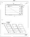
- (A) * (b) is explanatory drawing which shows typically the example which scans by dividing into 4 the backlight concerning Embodiment 1 of this invention.
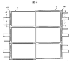
- FIG. 1 It is a top view which shows the example which made the liquid crystal display device concerning Embodiment 1 of this invention multi-panel. It is a block diagram which shows schematic structure of the liquid crystal panel concerning the modification of Embodiment 1 of this invention.
- (A) is a top view which shows schematic structure when the liquid crystal display device concerning Embodiment 2 of this invention is decomposed
- (b) is embodiment of this invention.
- 2 is a side view showing a schematic configuration of a liquid crystal display device according to FIG. (A) * (b) is explanatory drawing which shows typically the example which scans by dividing into 4 the backlight concerning Embodiment 2 of this invention.
- FIG. 11 is a plan view showing a schematic configuration of a conventional general liquid crystal display device using a TAB method.
- A) is a top view which shows schematic structure of the principal part of the liquid crystal display device using a TAB system
- (b) is when the liquid crystal display device shown to (a) is bent 90 degrees in the TAB module part.
- C) shows a side view when the liquid crystal display device shown in (a) is bent 180 ° at the TAB module portion.
- Embodiment 1 An embodiment of the present invention will be described below with reference to FIGS. 1A and 1B to FIG.
- FIG. 1A is a plan view showing a schematic configuration when the liquid crystal display device 100 according to the present embodiment is disassembled and viewed from the upper surface side (observer side) of each component.
- b) is a side view showing a schematic configuration of the liquid crystal display device 100 according to the present embodiment.
- the light emission side of the liquid crystal display device 100 that is, the observer side will be described as the upper side (front side), and the opposite side will be described as the lower side (back side).
- the liquid crystal display device 100 is a transparent liquid crystal display device (see-through type liquid crystal display device) including a transparent display unit capable of displaying an image (video) and transmitting a background. For this reason, the liquid crystal display device 100 can observe a display image with a background in a transparent display part (transparent display area).
- the liquid crystal display device 100 includes a liquid crystal panel 1, a backlight 2, and an FPC 3 (LCD (Liquid Crystal Display) -FPC for liquid crystal panel connected to the liquid crystal panel 1). ), A backlight FPC 4 (BL (Back Light) -FPC) connected to the backlight 2, and a frame (not shown) as a housing.
- LCD Liquid Crystal Display
- FPC 3 Liquid Crystal Display
- BL Back Light
- FPC 4 Back Light
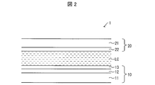
- FIG. 2 is a cross-sectional view illustrating a schematic configuration of a main part of the liquid crystal panel 1 according to the present embodiment.
- the liquid crystal panel 1 is an active matrix type liquid crystal panel in which a liquid crystal layer LC is sandwiched between a pair of transparent substrates 10 and 20 facing each other.
- a plurality of TFTs Thin Film Transistor 12 (switching elements, transistors), pixels on an insulating substrate 11 such as glass as an active matrix substrate
- an insulating substrate 11 such as glass
- a TFT substrate on which electrodes 13 and wirings, alignment films, etc. (not shown) are formed is used.
- a color filter substrate in which a common electrode 22 and a color filter, an alignment film or the like (not shown) are formed on an insulating substrate 21 such as glass is used.
- a polarizing plate or the like is provided on the surface (outside) opposite to the opposing surfaces of the substrates 10 and 20.
- the liquid crystal panel 1 has been described as a liquid crystal panel capable of displaying a color image in which a color filter is formed on the transparent substrate 20.
- the liquid crystal panel 1 is not limited to full color display, and is not limited to a single color or multiple colors. Also included are those that are displayed in color.
- the color filter may be provided on the transparent substrate 10.
- the liquid crystal panel 1 includes a monochrome display in which the color filter itself does not exist, or a display that performs display by a so-called field sequential method.
- the transmittance without the color filter is further increased, and high transparency can be obtained.
- the common electrode 22 may be provided on the transparent substrate 20 as described above, or may be provided on the transparent substrate 10 as a comb-tooth electrode.
- the driving method of the liquid crystal panel 1 is not particularly limited, and is a vertical electric field driving method using a so-called vertical electric field generated between the pixel electrode 13 provided on the transparent substrate 10 and the common electrode 22 provided on the transparent substrate 20.
- a lateral electric field driving method using a so-called lateral electric field generated between the pixel electrode 13 and the common electrode 22 provided on the transparent substrate 10 may be used.
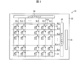
- FIG. 3 is a block diagram showing a schematic configuration of the liquid crystal display device 100 according to the present embodiment.
- the liquid crystal panel 1 includes a transparent substrate 10, a display region 31, a plurality of gate lines GL1, GL2, GL3,... GLn-1, GLn (n is an arbitrary integer, hereinafter these gate lines) Are collectively referred to as “gate line GL”), and a plurality of source lines SL1, SL2, SL3,... SLm ⁇ 1, SLm (m is an arbitrary integer, hereinafter these source lines are collectively referred to as “source line SL”). ”), An active matrix display panel in which the gate driver 33 and the source driver 34 are built.
- the display area 31 is a transparent display unit that displays video based on the video signal while performing background transparent display.
- the display area 31 is an area where a plurality of pixels PIX are arranged in a matrix. Although not shown, in the display region 31, a plurality of pixel electrodes 13 (see FIG. 2) are arranged in a matrix. Each pixel PIX includes a TFT 12, which is a selection element of the pixel PIX, a liquid crystal capacitor CL, and an auxiliary capacitor Cs. In addition, although not shown, an auxiliary capacitance line for applying an auxiliary capacitance voltage to each auxiliary capacitance Cs of the pixel PIX is formed.
- the gate electrode of the TFT 12 is connected to the gate line GL, and the source electrode of the TFT 12 is connected to the source line SL.
- the liquid crystal capacitor CL and the auxiliary capacitor Cs are connected to the drain electrode of the TFT 12.
- each of the plurality of gate lines GL includes n gate lines GL (gate lines GL1, GL2, GL3,... GLn ⁇ 1, GLn) extending in the row direction (left and right direction in FIG. 3). Are connected to the output of the gate driver 33, respectively.
- the plurality of source lines SL are each composed of m source lines SL (source lines SL1, SL2, SL3,..., SLm-1, SLm) extending in the column direction (vertical direction in FIG. 3). Are connected to the output of the source driver 34, respectively.
- the gate electrode, the source electrode, and the wiring group connected to them include, for example, a conductive material such as Cu (copper), Al (aluminum), Ti (titanium), Alternatively ITO (indium tin oxide), IZO (indium zinc oxide), Sn0 2 (tin oxide), ZnO (zinc oxide) optically transparent conductive material such as is used.
- a conductive material such as Cu (copper), Al (aluminum), Ti (titanium), Alternatively ITO (indium tin oxide), IZO (indium zinc oxide), Sn0 2 (tin oxide), ZnO (zinc oxide) optically transparent conductive material such as is used.
- a frame area 32 is provided around the display area 31.
- the gate driver 33 and the source driver 34 are formed in the frame region 32 as drive circuits for driving the liquid crystal panel 1.
- the gate driver 33 is provided in a region adjacent to the display region 31 on one side in the extending direction of the gate line GL.
- the source driver 34 is provided in the extending direction of the source line SL with respect to the display region 31. It is provided in a region adjacent to one side.
- the display area 31 of the liquid crystal panel 1 is a horizontally long screen
- the gate driver 33 is disposed on one of the vertical frame areas 32 on the left and right sides of the display area 31.
- the source driver 34 is disposed on one of the horizontal frame regions 32 on the upper and lower sides of the display region 31.
- the gate driver 33 and the source driver 34 are monolithic circuits built in the transparent substrate 10 and are configured by a semiconductor (peripheral TFT). Note that in FIGS. 1A to 1C to FIG. 3, illustration of wiring relating to panel driving including peripheral circuit TFTs and external connections (FPC mounting or the like) is omitted.
- the gate driver 33 and the source driver 34 are formed monolithically with the display region 31 using, for example, amorphous silicon, polycrystalline silicon, CG silicon (Continuous Grain) Silicon), microcrystalline silicon, or the like. .
- the gate driver 33 sequentially outputs a scan signal to the gate line GL, thereby switching the TFT 12 provided corresponding to each pixel electrode 13 in the display region 31 between ON (ON) and OFF (OFF).
- the source driver 34 inputs a video signal to the pixel electrode 13 from the TFT 12 that is turned on via the source line SL.
- the TFT 12 When a scan signal is supplied from the gate driver 33 to the gate electrode of the TFT 12 via the gate line GL, the TFT 12 is turned on and selected for each row. At this time, a signal voltage corresponding to the video signal is supplied from the source driver 34 to the source line SL, and the signal voltage is applied to each pixel electrode 13 belonging to the row selected via the source line SL via the TFT 12. When written, a potential difference is generated between the pixel electrode 13 and the common electrode 22, and a signal voltage is applied to the liquid crystal layer LC to change the alignment state of the liquid crystal molecules. As a result, an image (video) corresponding to the video signal is displayed in the display area 31.
- the liquid crystal panel 1 is connected via an FPC 3 to an external circuit (not shown) on which signal processing components are mounted.
- the frame region 32 of the transparent substrate 10 is further provided with a terminal portion 35 on which terminals for connecting the FPC 3 shown in FIG.
- the terminal part 35 is a mounting part of the FPC 3 in the liquid crystal panel 1.
- the video signal and the like are input to the liquid crystal panel 1 from the outside (external circuit) via the FPC 3.
- the terminal portion 35 is provided only on one side of the liquid crystal panel 1, and the one side is the same side as the side where the gate driver 33 is disposed (gate driver forming side, gate side).
- the gate driver 33 and the source driver 34 are monolithically formed in the frame area 32 around the display area 31.
- the formation positions of the gate driver 33 and the source driver 34 are not limited to this.
- the gate driver 33 and the source driver 34 may be monolithically formed in the display region 31.
- the backlight 2 is provided on the side opposite to the display surface (back side) of the liquid crystal panel 1 so as to emit light toward the liquid crystal panel 1. It has become.
- the backlight 2 according to this embodiment is an edge light type (side light type) illumination device.
- the backlight 2 is an LED substrate on which a transparent light guide plate 41 (transparent light guide plate) provided behind the liquid crystal panel 1 and an LED (light emitting diode) 43 (light source, see FIG. 4A) are mounted. 42 (backlight substrate, light source mounting substrate).
- an LED used as the light source
- an edge light type backlight light source backlight edge light
- the light source is not limited to the LED, and may be a solid-state light emitting element other than the LED, such as a laser diode.
- the material of the light guide plate 41 is not particularly limited as long as it is a transparent material.
- the backlight 2 indirectly irradiates the liquid crystal panel 1 indirectly by reflecting the light emitted from the LEDs 43 by the light guide plate 41.
- the LED substrate 42 is provided on one side of the light guide plate 41 in the scan (scanning, liquid crystal scan) direction of the liquid crystal panel 1, and one side of the liquid crystal panel 1 in the scan direction of the liquid crystal panel 1 is provided on the LED substrate 42.
- a plurality of LEDs 43 are mounted along the line.
- the backlight 2 is connected to the external circuit via the FPC 4.
- the LED substrate 42 is provided with an FPC connection portion (FPC connector connection portion, terminal portion) (not shown) on which terminals for connecting the FPC 4 are arranged.
- the FPC connection portion is provided on the same side of the backlight 2 as the LED 43 (edge light type backlight light source, more specifically, the LED substrate 42 on which the light source is mounted).
- the one side is a side corresponding to the side (gate side) where the gate driver 33 of the liquid crystal panel 1 is formed in the backlight 2, and the LED substrate 42 and the FPC connection portion provided on the LED substrate 42 are arranged in a liquid crystal display.
- the device 100 is assembled, it is provided on the same side as the gate driver 33 forming side (gate side).
- the FPC 3 inputs a video signal or the like for displaying an image (video) from the outside to the liquid crystal panel 1 by connecting the liquid crystal panel 1 and an external circuit (not shown).
- the liquid crystal panel 1 displays an image or the like based on a signal from an external circuit. Therefore, the liquid crystal panel 1 and the external circuit are connected by the FPC 3 for transmitting a display signal from the external circuit to the liquid crystal panel 1.
- the FPC 3 is connected to the terminal portion 35 in the liquid crystal panel 1.
- the terminal part 35 in the FPC 3 and the liquid crystal panel 1 is an external signal input / output part (external connection wiring mounting part) for controlling the liquid crystal panel, and between the liquid crystal panel 1 and an external circuit via the external signal input / output part. A display signal is exchanged.
- the FPC 3 is electrically connected to the gate driver 33 and the source driver 34 via the terminal portion 35.
- the FPC 4 supplies backlight power to the backlight 2 by connecting the backlight 2 and an external circuit (not shown).
- the FPC 4 is connected to the FPC connection unit in the backlight 2.
- the FPC connection part in the FPC 4 and the backlight 2 is an external signal input / output part (external connection wiring mounting part) for controlling the backlight substrate, and between the backlight 2 and the external circuit via the external signal input / output part. Then, the backlight signal is exchanged.
- the FPC 4 is electrically connected to the LED 43 via the FPC connection part.
- the FPC 3 and the terminal unit 35 functioning as an external signal input / output unit (first external connection wiring mounting unit) for controlling the liquid crystal panel, and an external signal input / output unit (second external connection wiring mounting for backlight control).
- the FPC 4 and the FPC connecting portion in the backlight 2 function as the FPC 3 forming side in the liquid crystal panel 1 and the FPC 4 forming side in the backlight 2 when the liquid crystal panel 1 and the backlight 2 are overlapped.
- the liquid crystal display device 100 is a transparent liquid crystal display device, and in the display region 31, the back image can be visually recognized (observation of the background) through the liquid crystal panel 1 and the backlight 2. The display image can be observed together with the background.
- the liquid crystal panel 1 and the backlight 2 are accommodated in a frame (housing) (not shown) having openings on the front and back surfaces of the display area 31.
- the liquid crystal display device 100 exposes the display area 31 in the liquid crystal panel 1 from the opening on the front side of the frame, and overlaps the display area 31 of the liquid crystal panel 1 in the backlight 2 from the opening on the back side of the frame. The exposed area is exposed.
- no component (structure) that prevents transparent display is arranged in order to make the liquid crystal display device 100 function as a transparent display device.
- the outer frame of the liquid crystal panel 1 hinders the transparency as a design. For this reason, it is desirable that the frame region 32 serving as the outer frame portion of the liquid crystal panel 1 has each side as narrow as possible and ideally does not exist.
- both the gate driver 33 and the source driver 34 are monolithic, and the FPC 3 connected to the external circuit is mounted (mounted) on the liquid crystal panel 1 so that the driver TAB (the source driver TAB and the gate driver 34) is mounted.
- the driver TBA the source driver TAB and the gate driver 34
- the driver substrate gate substrate and source substrate
- the length of the source side (side where the source driver is arranged, source driving side) is 700 mm
- the length of the gate side (side where the gate driver is arranged, gate driving side)
- the length of the frame region in the liquid crystal display device 300 shown in FIG. 12A is usually about 25 mm for the source side and about 35 mm for the gate side.
- the frame region accompanying the monolithic structure of the gate driver 33 and the source driver 34 (that is, the increase in the liquid crystal panel side with respect to the display region 31 accompanying the monolithic structure) is 10 mm or less at the source side.
- the gate side is 10 mm or less.
- the balance of the four sides of the frame changes depending on the layout of the gate driver 33 and the source driver 34 around the display area 31 on the liquid crystal panel 1, but as described above, the gate driver 33 and the source driver 34 are monolithic. By adopting a structure, the effect of the above numerical values can be expected as a whole.
- the gate driver 33 and the source driver 34 are monolithic as described above, and the FPC 3 connected to the external circuit is mounted (mounted) on the liquid crystal panel 1, whereby the liquid crystal on the driver substrate is mounted. It is possible to eliminate the influence on the display area 31 (transparent display area) due to the folding of the panel 1 to the back side.
- the gate driver 33 and the source driver 34 have a monolithic structure, and the external connection wiring mounting portion (external signal input / output portion) in the liquid crystal panel 1 associated with the monolithic structure is replaced with the gate driver 33. It is put together on one side (gate side) where is provided.
- the backlight 2 has an edge light type structure, and the edge scan for backlight (for example, the LED 43) and the external connection wiring mounting portion (external signal input / output portion) in the backlight 2 are provided with a gate scan provided with a gate driver 33. Arranged only on one side (gate side).
- the external connection wiring mounting portion (first external connection wiring mounting portion) in the liquid crystal panel 1 and the external connection wiring mounting portion (second external connection wiring mounting portion) in the backlight 2 are connected to the liquid crystal display device 100.
- the three sides of the liquid crystal panel 1 (liquid crystal display device 100) can be made as free as possible (no load or external wiring connection), so the liquid crystal panel 1 (liquid crystal display device 100). Of these four sides, three sides can be narrowed.
- the gate driver 33 and the source driver 34 are monolithically built in the liquid crystal panel 1 as described above, it is not necessary to externally attach the gate driver and the source driver. 33 and the source driver 34 can be formed simultaneously with the display area 31.
- the liquid crystal panel generally has a problem in the response speed of the liquid crystal.
- One means for suppressing this problem is a method of scanning the backlight in synchronization with the scan of the liquid crystal panel.
- the scanning direction of the backlight needs to match the scanning direction of the liquid crystal panel.
- the LED 43 is used as a light source in a plan view, that is, the liquid crystal display device 100 is viewed from the observer side, as shown in FIGS.
- the liquid crystal display device 100 is disposed on one of the left and right sides (gate sides).
- the backlight 2 is scanned by the backlight scan in which the plurality of LEDs 43 are intermittently lit within one frame period (within the image frame period) in synchronization with the liquid crystal scan with respect to the gate scan direction. Can be driven.
- 4A and 4B are explanatory views schematically showing an example in which the backlight 2 (LED substrate 42) is divided into four and scanned.
- the gate driver 33 is divided into four, and the backlight 2 is divided into four lines (areas) corresponding to the divided gate drivers 33, and any one of the lines is always lit. Thus, the lighting / extinguishing of the LED 43 is controlled for each line.
- the lighting timing of the LED 43 rows is controlled so that only the video portion is lit in synchronization with the liquid crystal scanning timing (video signal), and the LEDs 43 are sequentially turned on (backlight scan) by being turned on / off.
- the backlight 2 is time-divided, and by irradiating the backlight 2 only during a period in which the writing charge reaches a certain level, The period during which the same image is displayed can be shortened, and pseudo impulse driving can be realized.
- moving image performance can be improved and the display performance (display quality) as a liquid crystal display device can be improved.
- FIG. 5 is a plan view showing an example in which the liquid crystal display device 100 is made into a multi-panel.
- the liquid crystal display device 100 (the liquid crystal panel 1 and the backlight 2) shown in FIGS. Show.
- the external connection wiring mounting portion of the liquid crystal panel 1 and the backlight 2 and the LED 43 (light source) are arranged on one side of the liquid crystal panel 1 (liquid crystal display device 100) in plan view.
- the backlight 2 has a scan backlight structure, and the backlight 2 can be partially lit (backlight irradiation) by being driven by the backlight scan method as described above. It becomes.
- the light source (for example, LED 43) of the upper half block of the backlight 2 is turned on to display an image only on the upper half block of the liquid crystal panel 1 corresponding to the block.
- the lower half block of 2 is not lit, and the lower half block of the liquid crystal panel 1 corresponding to the block can be displayed so that the image is not displayed and is in a transparent state.
- FIG. 1A and FIG. 3 the case where the gate driver 33 and the source driver 34 are provided only on one side with respect to the display region 31 has been described as an example. However, the gate driver 33 and the source driver 34 may be provided on one side (one side) with respect to the display region 31 or may be provided on both sides (two sides).
- the gate driver 33 is provided on two sides of the display area 31, and the source driver 34 is provided on the other two sides of the display area 31 (two sides different from the two sides on which the gate driver 33 is provided). An example will be described.
- FIG. 6 is a block diagram showing a schematic configuration of the liquid crystal panel 1 according to the present modification.
- the liquid crystal panel 1 includes a display region 31, a plurality of gate lines GL, a plurality of source lines SL, gate drivers 33 a and 33, and source drivers 34 a and 34 b on a transparent substrate 10. Is an active matrix type display panel.
- the pixel PIX includes the TFT 12, the liquid crystal capacitor CL, and the auxiliary capacitor Cs, and an auxiliary capacitor line (not shown) is formed in the display region 31.
- the gate electrode of the TFT 12 is connected to the gate line GL, and the source electrode of the TFT 12 is connected to the source line SL.
- the liquid crystal capacitor CL and the auxiliary capacitor Cs are connected to the drain of the TFT 12.
- the gate driver 33a and the gate driver 33b are arranged so as to sandwich the display area 31 therebetween.
- the first group of gate lines GL including the gate lines GL1, GL3,.
- the second group of gate lines GL consisting of the remaining gate lines GL2, GL4,... Is connected to the output of the gate driver 33b.
- a first group of source lines SL composed of every other source line SL1, SL3,.
- the second group of source lines SL composed of the remaining source lines SL2, SL4,... are connected to the output of the source driver 34b.
- each of the gate driver 33 and the source driver 34 may be provided on one side of the liquid crystal panel 1 or may be provided on two sides. Although not shown, only the gate driver 33 of the four sides of the liquid crystal panel 1 may be provided on two sides, the source driver 34 may be provided only on one side, and only the source driver 34 is provided on two sides. The gate driver 33 may be provided only on one side.
- the FPC 3 and the terminal portion 35 on which the FPC 3 is mounted are arranged with the gate driver 33 in plan view.
- the liquid crystal panel 1 is provided only on one side.
- both the gate driver 33 and the source driver 34 are monolithically built in the liquid crystal panel 1 has been described as an example, but one has a monolithic structure and the other is a COG. (Chip ⁇ On Glass) mounting or COF (Chip on Film) mounting may be employed.
- COG Chip ⁇ On Glass
- COF Chip on Film
- the FPC (FPC 3 or 4) is used for a connection part (interface part) with an external circuit, and signals and power are supplied (transmitted) to the liquid crystal panel 1 and the backlight 2 by the FPC.
- connection means such as a cable may be used as the interface unit (external connection wiring mounting unit).
- Embodiment 2 The following will describe another embodiment of the present invention with reference to FIGS. 7A and 7B and FIGS. 8A and 8B.
- differences from the first embodiment will be mainly described, and the description of the same configuration will be omitted.
- symbol is attached
- FIG. 7A is a plan view showing a schematic configuration when the liquid crystal display device 100 according to the present embodiment is disassembled and viewed from the upper surface side of each component
- FIG. 1 is a side view illustrating a schematic configuration of a liquid crystal display device 100 according to an embodiment.
- a support base (not shown) in the liquid crystal display device 100 is used.
- the support is provided on the lower side of the long side of the liquid crystal panel 1 (liquid crystal display device 100).
- the liquid crystal panel 1 (the liquid crystal display device 100) are narrow frames, it is ideal as a design to select the upper side and the left and right sides as the sides to be narrowed. In addition, it can be used for a wide range of applications.
- the gate driver 33 is disposed on the long side among the respective sides of the liquid crystal panel 1 (the liquid crystal display device 100), and the source driver 34 is disposed on the short side.
- the gate driver 33 is disposed on the lower side which is one of the long sides of the liquid crystal panel 1 (the liquid crystal display device 100), and
- the source driver 34 is arranged on one side (the right side in the example shown in FIGS. 7A and 7B) of the short sides of the liquid crystal panel 1 (the liquid crystal display device 100).
- the gate driver 33 and the source driver 34 are both monolithically built in the liquid crystal panel 1 as in the first embodiment.
- the FPC 3 that is the external connection wiring mounting portion (first external connection wiring mounting portion) and the terminal portion 35 (see FIGS. 3 and 6) in the liquid crystal panel 1 are one side of the gate side of the liquid crystal panel 1. Only provided.
- the backlight 2 is an edge light type, and includes an edge light for backlight (LED 43), and an FPC 4 and an FPC connection portion which are external connection wiring mounting portions (second external connection wiring mounting portions) in the backlight 2. Provided on the gate side.
- the LED substrate 42 and the FPCs 3 and 4 on which the LEDs 43 are mounted are arranged on the lower side of the liquid crystal panel 1 (the liquid crystal display device 100). Established.
- the gate driver 33 and the source driver 34 have a monolithic structure, and the external connection wiring mounting portion of the liquid crystal panel 1 and the backlight 2 and the LED 43 (light source) of the liquid crystal panel 1 (liquid crystal display device 100) are viewed in plan view. By concentrating on one side, the same effect as in the first embodiment can be obtained.
- the scanning direction of the liquid crystal is the left-right direction by arranging the gate driver 33 on the long side and the source driver 34 on the short side.
- 8A and 8B schematically show an example in which the backlight 2 (LED substrate 42) is divided into four parts and scanned in this embodiment.
- the scanning direction is changed from that in the first embodiment, and in this embodiment, as in the first embodiment, the scan in the liquid crystal is synchronized with the gate scanning direction. Backlight scanning becomes possible.
- the moving image performance can be improved as in the first embodiment, and the display performance (display quality) as the liquid crystal display device can be improved.
- the liquid crystal display device 100 when the liquid crystal display device 100 according to the present embodiment is made into a multi-panel, the liquid crystal display device 100 is arranged so that the sides where the FPCs 3 and 4 are arranged are aligned in a plan view as in the example shown in FIG. Needless to say, the panel 1 and the backlight 2 may be provided.
- the case where the liquid crystal panel 1 has a horizontally long rectangular shape with the long side in the horizontal direction and the short side in the vertical direction has been described as an example.
- the support base is generally provided on the lower side of the liquid crystal panel 1 (the liquid crystal display device 100). Therefore, when the support base is provided on the lower side of the liquid crystal panel 1 (the liquid crystal display device 100) as described above, the upper side and the left and right sides are used as the sides to be narrowed as described above regardless of the shape of the liquid crystal panel 1.
- the design can be improved and a wide range of applications can be supported. It becomes.
- FIGS. 9 (a) and 9 (b) Still another embodiment of the present invention will be described below with reference to FIGS. 9 (a) and 9 (b).
- differences from the first embodiment will be mainly described, and the description of the same configuration will be omitted.
- symbol is attached
- FIG. 9A is a plan view showing a schematic configuration when the liquid crystal display device 100 according to the present embodiment is disassembled and viewed from the upper surface side of each component
- FIG. 9B is a plan view.
- 1 is a side view illustrating a schematic configuration of a liquid crystal display device 100 according to an embodiment.
- the liquid crystal display device 100 is arranged by a COG (Chip On Glass) system in which the gate driver 33 and the source driver 34 are directly mounted and connected to the input / output terminals of the transparent substrate 10 using an IC or LSI. Except for having a COG structure provided (COG mounting), it is the same as the first embodiment.
- a plurality of IC chips (gate driver ICs) are arranged on one side (upper side) of the transparent substrate 10 as the gate driver 33, and a plurality of sort drivers 34 are used.
- the IC chip (source driver IC) is arranged on the other side (right side) of the transparent substrate 10 as an example.
- the gate driver 33 and the source driver 34 are directly disposed (mounted) on the liquid crystal panel 1 by the COG method using the driver IC, so that the liquid crystal panel 1 (the liquid crystal display device 100 is mounted). ) Can be reduced as much as possible.
- the gate driver 33 and the source driver 34 can be driven without mounting a driver IC or driver LSI on the transparent substrate 10. For this reason, by forming the gate driver 33 and the source driver 34 monolithically, it is not necessary to design and develop a liquid crystal panel according to the IC or LSI to be used. Further, when the gate driver 33 and the source driver 34 are formed monolithically, the number of input signal lines is small, so that the wiring pitch can be widened, the FPC 3 can be easily connected, and the connection reliability is improved. In addition, since the demand for connection accuracy is reduced, productivity can be improved.
- one of the gate driver 33 and the source driver 34 may be formed monolithically and the other may be COG mounted.
- the gate driver 33 and the source driver 34 preferably have a monolithic structure or a COG structure as described above in order to make the frame narrower.
- one of the gate driver 33 and the source driver 34 is monolithic.
- COF structure in which a driver IC or a driver LSI used as the gate driver 33 or source driver 34 is directly mounted on the FPC (COF mounting) by a COF (Chip-on-Film) system. It does not matter.
- the gate driver 33 that can be easily made monolithic may have a monolithic structure, and the source driver 34 may have a COG structure or a COF structure.
- the mounting method may be different between one and the other if necessary.
- at least one of the gate driver 33 disposed on one side of the liquid crystal panel 1 and the source driver 34 disposed on the other side of the liquid crystal panel 1 has a COG structure or a monolithic structure. Good.
- the FPC used for mounting the gate driver 33 or the source driver 34 is provided separately from the FPC 3.
- a plurality of FPCs on which driver ICs are mounted are arranged along one side of the liquid crystal panel in plan view.
- the driver IC mounted on each FPC is connected to the output terminal of the driver IC of the preceding FPC by connection wiring (peripheral wiring arranged around the display area 31) (not shown).
- the first FPC driver IC is electrically connected to the FPC 3 by connection wiring (not shown).
- the COF method may be used for mounting the gate driver 33 or the source driver 34, and the COF method used here does not require a driver substrate such as a gate substrate or a source substrate, so-called.
- a driver substrate such as a gate substrate or a source substrate
- the FPC 3 connected to the external circuit is directly disposed on the liquid crystal panel 1, so that the display region 31 (transparent display) by folding the driver substrate to the back side of the liquid crystal panel 1. Area) can be eliminated.
- At least one (at least one) of the gate driver 33 and the source driver 34 has a monolithic structure or a COG structure, so that the gate driver and the source driver are respectively mounted on the TAB. Compared to the case, the frame can be narrowed.
- the folding position is limited, whereas the FPC used in the COF method has an advantage that the bending position is not limited and the bending is free.
- the gate driver 33 and the source driver 34 have a COG structure or a monolithic structure, the gate driver 33 and the source driver 34 are directly mounted on the liquid crystal panel 1 without using a tape carrier. (Mounting) can be performed, and the gate driver 33 and the source driver 34 are not required to be externally attached.
- the gate driver 33 and the source driver 34 have a COG structure or a monolithic structure, the frame can be narrowed, the number of parts can be reduced, and an inexpensive configuration can be achieved.
- the gate driver 33 is disposed on the short side and the source driver 34 is disposed on the long side of each side of the liquid crystal panel 1 (liquid crystal display device 100).
- the gate driver 33 is disposed on the long side among the sides of the liquid crystal panel 1 (the liquid crystal display device 100), and the source driver 34 is disposed on the short side. Needless to say, may be provided. Also in the present embodiment, the same modifications as in the first and second embodiments can be performed.
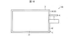
- FIG. 10 is a plan view showing a schematic configuration of the liquid crystal display device 100 according to the present embodiment.
- the gate driver 33, the source driver 34, the terminal portion 35, and the like are not shown.
- the liquid crystal panel 1 connected to the terminal portion 35 (see FIG. 3 or FIG. 6) on which the gate driver 33, the source driver 34, and the FPC 3 are mounted as the peripheral wiring 36. Wiring relating to driving is provided.
- a gate driver 33, a source driver 34, a terminal portion 35, and a peripheral wiring 36 are arranged around a display area 31 in the liquid crystal panel 1 as shown in FIG. 100) are arranged so as to have a uniform width.
- the gate driver 33 and the source driver 34 are assumed to be built in the liquid crystal panel 1, for example, monolithically.
- the LED substrate 42 on which the LEDs 43 (for example, see FIG. 4A) are mounted is provided with the gate driver 33, the source driver 34, the terminal portion 35, and the peripheral wiring 36 in plan view.
- the LED substrate 42 is provided so as to be located in the region.
- the LED 43 in the backlight 2 and the FPC 4 and the FPC connection part functioning as the second external connection wiring mounting part are located in the frame region 32 on the side where the gate driver 33 is provided.
- the widths of the four frames of the liquid crystal panel can be made uniform.
- the frame as a transparent display device is made as thin as possible so that its presence is not noticeable, and the balance of the four sides of the frame is balanced. Can keep. For this reason, design property can be improved.
- the liquid crystal display device 100 according to the first embodiment has been described as an example of modification.
- the liquid crystal display device 100 according to the second or third embodiment is modified as described above. Needless to say, it's also good.
- the transparent liquid crystal display device (liquid crystal display device 100) according to aspect 1 of the present invention includes a gate driver 33, a source driver 34, and a first external connection wiring mounting portion (for example, the FPC 3 and the terminal portion 35) connected to an external circuit. ) And a backlight 2 provided with a second external connection wiring mounting portion (for example, FPC 4 and FPC connection portion) connected to an external circuit, and the liquid crystal panel 1 and the back A transparent liquid crystal display device capable of observing the background through the light 2, wherein the gate driver 33 is disposed on one or two sides of the liquid crystal panel 1, and the source driver 34 is connected to the liquid crystal panel 1.
- a gate driver 33 is disposed on one or two sides of the liquid crystal panel 1
- the source driver 34 is connected to the liquid crystal panel 1.
- At least one of the gate driver 33 and the source driver 34 is disposed on one or two other sides, and has a COG structure or a monolithic structure.
- the backlight 2 is an edge light type backlight in which a light source (for example, LED 43) is disposed on one side of the light guide plate 41, and the first and second external connection wiring mounting portions, The light sources are arranged on the same side in a plan view, and the one side is an arrangement side of the gate driver 33.
- the gate driver 33 and the source driver 34 has a COG structure or a monolithic structure, and the liquid crystal panel 1 has an external circuit separately from the gate driver 33 and the source driver 34. Since the first external connection wiring mounting portion (for example, the FPC 3 and the terminal portion 35) to be connected is directly provided, it is unnecessary to mount the driver TAB and dispose a driver substrate such as a gate substrate or a source substrate. become. For this reason, it is possible to narrow the frame area of the liquid crystal panel on the side where the driver is provided, as compared with the case where the gate driver and the source driver are mounted by TAB.
- At least one of the gate driver 33 and the source driver 34 has a COG structure or a monolithic structure, and the liquid crystal panel 1 is connected to an external circuit.
- the external connection wiring mounting portion it is possible to eliminate the influence on the display area 31 due to the folding of the driver substrate to the back surface side of the liquid crystal panel 1.
- the first and second external connection wiring mounting portions and the light source are arranged (aggregated) on the same side (the side where the gate driver 33 is provided), whereby a liquid crystal panel 1 (the liquid crystal display device 100) can be made as free as possible (no load or external wiring connection), so that the three sides of the four sides of the liquid crystal panel 1 (the liquid crystal display device 100) are narrowed. Can do.
- the said 1st and 2nd external connection wiring mounting part and the said light source are arrange
- the first and second external connection wiring mounting portions and the light source are arranged (aggregated) on the side where the gate driver 33 is disposed, so that the backlight scanning method is used.
- the light 2 can be driven.
- the backlight 2 is driven by the backlight scanning method, the moving image performance can be improved, and the display performance (display quality) as a liquid crystal display device can be improved.
- the gate driver 33 and the source driver 34 in the aspect 1 may have a COG structure or a monolithic structure.
- the gate driver 33 and the source driver 34 can be directly mounted (mounted) on the liquid crystal panel 1 without using a tape carrier. It becomes unnecessary.
- the frame can be narrowed, the number of parts can be reduced, and an inexpensive configuration can be achieved.
- the light source for example, the LED 43
- the light guide plate 41 in the first or second aspect.
- the light 2 may be driven by a backlight scanning method in which the plurality of light sources are sequentially intermittently turned on.
- the period during which the same image is displayed can be shortened, and pseudo impulse driving can be realized. For this reason, moving image performance can be improved, and display performance (display quality) as a liquid crystal display device can be improved.
- the liquid crystal panel 1 has a rectangular shape having a long side and a short side, and the gate driver 33 may be disposed on the long side of the liquid crystal panel 1, and the source driver 34 may be disposed on the short side of the liquid crystal panel 1.
- the liquid crystal panel 1 (the display area 31 of the liquid crystal panel 1) is a general horizontally long rectangle (for example, the aspect ratio is 16: 9)
- the support base is usually a liquid crystal display. It is provided on the lower side of the long side of panel 1 (liquid crystal display device 100).
- a gate driver 33 is disposed on the long side of the liquid crystal panel 1 (liquid crystal display device 100), a source driver 34 is disposed on the short side, and the first driver is disposed on one side of the long side.
- the transparent liquid crystal display device (liquid crystal display device 100) according to aspect 5 of the present invention is the gate driver 33, the source driver 34, or the first external connection wiring mounting portion (for example, the liquid crystal display device 100) according to any one of the aspects 1 to 4.
- FPC 3 and terminal portion 35), and peripheral wiring 36 arranged around display area 31 in liquid crystal panel 1 so that frame area 32 outside display area 31 of liquid crystal panel 1 has an equal width.
- the light source (for example, LED 43) and the second external connection wiring mounting portion (for example, FPC4 and FPC connection portion) are arranged in the frame region on the side where the gate driver 33 is disposed in plan view. 32 may be located.
- the widths of the four sides of the liquid crystal panel (liquid crystal display device 100) can be made uniform. Therefore, according to the above configuration, it is possible to keep the balance of the frame widths of the four sides while making the frame as thin as possible as a transparent display device so that its presence is not noticeable. For this reason, design property can be improved.
- the gate driver 33 may be disposed on the lower side of the liquid crystal panel 1.
- the support base When providing a support base in the liquid crystal display device 100, the support base is generally provided on the lower side of the liquid crystal panel 1 (the liquid crystal display device 100). Therefore, as the sides to be narrowed in the liquid crystal panel 1 (the liquid crystal display device 100), three sides of the upper side and the left and right sides are selected, and the first and second external connection wiring mounting portions and the light source are used as the liquid crystal. By disposing on the lower side of the panel 1 (liquid crystal display device 100), the design can be improved and a wide range of applications can be handled.
- the gate driver 33 and the source driver 34 may each have a monolithic structure. .
- the gate driver 33 and the source driver 34 are monolithically built in the liquid crystal panel 1, it is not necessary to externally attach the gate driver and the source driver.
- the display area 31 can be created at the same time.
- the gate driver 33 and the source driver 34 are monolithically built in the liquid crystal panel 1, so that the gate driver 33 and the source driver are not mounted on the liquid crystal panel 1 without mounting a driver IC or a driver LSI.
- the driver 34 can be driven. For this reason, it is not necessary to design and develop a liquid crystal panel according to the IC or LSI to be used.
- the gate driver 33 and the source driver 34 are formed monolithically, the wiring pitch can be widened because the number of input signal lines is small, the external connection wiring mounting portion can be easily connected, and the connection Reliability is improved and demand for connection accuracy is lowered, so that productivity can be improved.
- the gate driver 33 and the source driver 34 may each have a COG structure. .
- the presence of the three sides of the liquid crystal panel 1 (the liquid crystal display device 100) can be reduced as much as possible because the gate driver 33 and the source driver 34 each have a COG structure.
- the gate driver 33 has a monolithic structure and the source driver 34 has a COG structure. It may be.
- the gate driver is easier to make monolithic than the source driver. Therefore, only the gate driver 33 that can be easily made monolithic may have a monolithic structure, and the source driver 34 may have a COG structure.
- the present invention can be applied to a display device equipped with a see-through display device.
- liquid crystal panel 2 backlight FPC (first external connection wiring mounting part) 4 FPC (second external connection wiring mounting part) 10 Transparent substrate 11 Insulating substrate 12 TFT 13 pixel electrode 20 transparent substrate 21 insulating substrate 22 common electrode 31 display region 32 frame region 33, 33a, 33b gate driver 34, 34a, 34b source driver 35 terminal portion (first external connection wiring mounting portion) 36 Peripheral wiring 41 Light guide plate 42 LED substrate 43 LED (light source) 100 Liquid crystal display device 300 Liquid crystal display device 301 Liquid crystal panel 302 Display region 303 Frame region 310 TAB module 311 Semiconductor chip 321 Source substrate 330 TAB module 331 Semiconductor chip 341 Gate substrate 441 Wiring 442 FPC GL gate line SL source line LC liquid crystal layer PIX pixel
Landscapes
- Engineering & Computer Science (AREA)
- Chemical & Material Sciences (AREA)
- Crystallography & Structural Chemistry (AREA)
- Physics & Mathematics (AREA)
- Computer Hardware Design (AREA)
- General Physics & Mathematics (AREA)
- Theoretical Computer Science (AREA)
- Liquid Crystal (AREA)
Abstract
シースルー型の液晶表示装置(100)は、ゲートドライバ(33)およびソースドライバ(34)の少なくとも一方はCOG方式またはモノリシックにより配設されており、バックライト(2)がエッジライト型であり、平面視で、バックライト(2)の光源と、液晶パネル(1)に実装されたFPC(3)と、バックライト(2)に実装されたFPC(4)とが、ゲートドライバ(33)の配設辺に集約されている。
Description
本発明は、液晶パネルおよびバックライトを通して背景の観察が可能なシースルー型の透明液晶表示装置に関する。
近年、インテリアデザイン性やインタラクティブ性の向上等の観点から、シースルーディスプレイあるいは透明ディスプレイと称される、いわゆる透明表示装置(シースルー型表示装置)が注目されている。
透明表示装置は、その背後の物体を画面越しに観察したり、透明表示装置を、例えば自動車のインストルメントパネル等、様々な表示の前面に配置することで、透明表示装置による表示と、透明表示装置の背面側にある表示とを切り換えて表示したりすることが可能である。このため、様々な用途への利用が期待されている。
透明表示装置としては、有機EL(エレクトロルミネッセンス)素子を用いた透明有機EL表示装置がよく知られている(例えば特許文献1等、参照)。
有機EL表示装置の表示部は、発光体である有機物を陰極および陽極で挟むように積層して有機EL素子を形成し、該有機EL素子を画素として二次元的に多数配列してなる。例えば陰極および陽極に透明電極を使用することで、透明有機EL表示装置が実現される。
陰極および陽極の各端部には引出配線が接続されており、これらの引出配線は、FPC(Flexible Printed Circuit board;フレキシブルプリント回路基板)により表示部の外部に引き出され、駆動用のIC(集積回路)と電気的に接続されている。このため、有機EL表示装置の表示部周辺には、配線あるいは引出配線、FPC等が配置されており、いわゆる額縁が、一定幅で存在している。
しかしながら、透明表示装置は、その用途にもよるが、ディスプレイとしてのデザイン性が重要視されることが多い。例えばディスプレイとしての透明感を重要視する場合、ディスプレイ自体の存在感を可能な限り消す(隠す)必要がある。このため、透明表示装置のデザインとしては、透明感を阻害するような付属物を極力省くことが求められる。
例えば液晶表示装置で透明表示装置を実現する場合を考えると、液晶パネルの外枠は、デザインとしての透明感を阻害する。このため、液晶表示装置で透明表示装置を実現する場合、液晶表示装置に用いられる液晶パネルの外枠は、各辺が、極力狭く、理想的には存在しないことが望ましい。
しかしながら、液晶パネルには、一般的に、ゲートドライバが、液晶パネルの左辺および右辺のうち少なくとも一方に配置されているとともに、ソースドライバが、液晶パネルの上辺および下辺のうち少なくとも一方に配置されている。これにより、液晶パネルを駆動するための駆動信号および映像信号が、有線接続で入力されている。
ゲートドライバおよびソースドライバの実装には、一般的には、TAB(Tape Automated Bonding)方式が用いられる(例えば特許文献2等、参照)。
図11は、TAB方式を用いた、従来の一般的な液晶表示装置300の概略構成を示す平面図である。なお、図11では、ソースドライバが表示領域302の一方側(額縁領域303の1辺)のみに設けられており、ゲートドライバも表示領域302の一方側(つまり、額縁領域303の他の1辺)のみに設けられている場合を例に挙げて図示している。
図11に示すように、TAB方式を用いた液晶表示装置300では、液晶パネル301のソースライン(図示せず)を駆動するための半導体チップ311が実装されたTAB(Tape Automated Bonding)モジュール310により、ソース基板321と液晶パネル301とが接続される。また、液晶パネル301のゲートライン(図示せず)を駆動するための半導体チップ331が実装されたTABモジュール330により、ゲート基板341と液晶パネル301とが接続される。TABモジュール310・330に実装される半導体チップには、フィルム実装型のIC(集積回路)やLSI(大規模集積回路)が用いられている。
TABモジュール310は、ソースドライバ(ソースドライバTAB)として用いられ、TABモジュール330は、ゲートドライバ(ゲートドライバTAB)として用いられる。
ソース基板321およびゲート基板341は、TABモジュール310・330に映像信号や駆動電力を供給するための電子回路が搭載されたドライバ基板(駆動用プリント基板)である。
ソース基板321とゲート基板341とは、配線441により電気的に接続されている。ソースドライバおよびゲートドライバに与えられる各種信号は、ソース基板321に設けられたFPC(Flexible Printed Circuit board:フレキシブルプリント回路基板)442から供給される。
このように、液晶表示装置300には、一般的には、液晶パネル301における表示領域302周辺の額縁領域303に、TAB方式によりソースドライバおよびゲートドライバが形成(TAB実装)されている。
このため、透明表示装置に液晶表示装置300を用いる場合、現実的には、透明表示装置としての外枠の存在を消すことは難しい。
なお、図11に示すようにソースドライバおよびゲートドライバが表示領域302の一方側に設けられている場合、ソースドライバおよびゲートドライバが設けられていない額縁領域303の幅を、他の額縁領域303の幅よりも狭くすることはできる。
しかしながら、ソースドライバおよびゲートドライバが設けられている額縁領域には一定幅が必要であるとともに、液晶表示装置において一般的に使用されているソース基板321およびゲート基板341は、液晶パネル301の額縁幅が広くなる要因となっている。以下に、この理由について説明する。
図12の(a)は、TAB方式を用いた液晶表示装置300の要部の概略構成を示す平面図であり、図12の(b)は、図12の(a)に示す液晶表示装置300をTABモジュール310の部分で90°折り曲げたときの側面図を示し、図12の(c)は、図12の(a)に示す液晶表示装置300をTABモジュール310の部分で180°折り曲げたときの側面図を示す。
図12の(a)では、ソースドライバおよびゲートドライバがそれぞれ表示領域302の一方側に設けられており、ソースドライバおよびゲートドライバが設けられていない額縁領域303の幅を、他の額縁領域303の幅よりも狭くした場合を例に挙げて示している。
なお、図12の(a)~(c)では、図面の簡略化のために、配線441およびFPC442を省略するとともに、ソース基板321およびTABモジュール310・330の数を省略している。
図12の(b)・(c)に示すように、液晶表示装置300をTABモジュール310の部分で折り曲げれば、液晶表示装置300の額縁をある程度狭くすることができる。
しかしながら、液晶表示装置300を透明表示装置に用いる場合、液晶表示装置300を、TABモジュール310の部分で、図12の(b)に示すように90°、あるいは、図12の(c)に示すように180°折り曲げると、表示領域302から、折り曲げたソース基板321およびそれに接続された配線(図示せず)等が視認されてしまう。これは透明表示装置としては、致命的な欠点となる。
なお、特許文献2、3には、液晶パネルの一例として、COG(Chip On Glass)型の液晶パネルについて開示がなされている。
しかしながら、特許文献2の液晶表示装置は、耐衝撃性強化のため、液晶パネルと該液晶パネルに接続されたFPCとの間に例えば金属製の補強板を備え、液晶パネルを収容するフレームに金属製のフレームを使用している。耐衝撃性のためのこのような金属製のフレームや補強板等は、額縁の存在を際立させる。
また、特許文献2の液晶表示装置は、コネクタ部、アンテナ特性チェック用ピンコネクタ部、スピーカ等が、液晶表示装置の裏面(表示面とは反対側)全体に配置されている。特にフレームにより、液晶パネルの裏面側が完全に覆われている。このため、特許文献2の液晶表示装置は、透明表示装置として使用することはできない。
同様に、特許文献3に記載の液晶表示装置も裏面が筐体で覆われており、該筐体裏面側に、例えば外部接続用端子や記録媒体挿入部等が設けられる。
また、有機EL表示装置とは異なり、液晶表示装置の表示には、基本的に、光源となるバックライトが必要である。
バックライトは、主に、特許文献2に開示されているようなエッジライト型と、特許文献3に開示されているような直下型とに大別される。
直下型のバックライトは、液晶パネルの背後に複数配列された光源により液晶パネルを直接照射する。
これに対し、エッジライト型のバックライトは、液晶パネルの背後に設けられた導光板の端面に光源が設けられており、光源から出射した光を導光板で反射させることにより、液晶パネルを間接的に均一照射する。このため、エッジライト型のバックライトは、薄型化が可能で、輝度均一性に優れている。
しかしながら、このようにエッジライト型のバックライトを用いる場合、最低でも液晶パネルの一辺に、LED(発光ダイオード)等の光源を配置する必要がある。
このため、透明表示装置に液晶表示装置を用いる場合、液晶パネルを駆動するためのソースドライバTABおよびゲートドライバTABのみならず、エッジライト型のバックライトの光源(LED等)および該光源に駆動用電力を供給するバックライト用FPCの接続部等が設けられるLED基板等のバックライト基板によっても一定の幅の額縁領域を必要とする。
また、液晶パネルは、一般的に液晶の応答速度に課題がある。画質向上のためにバックライトをスキャンする場合、バックライトのスキャン方向は、液晶パネルのスキャン方向と一致させておく必要がある。
しかしながら、特許文献2には、液晶パネル用FPCおよびバックライト用FPCの接続辺について何の具体的な記載もされていない。
本発明は、上記問題点に鑑みなされたものであり、その目的は、狭額縁でデザイン性に優れるシースルー型の透明液晶表示装置を提供することにある。また、本発明のさらなる目的は、狭額縁でデザイン性に優れるとともに、表示性能に優れたシースルー型の透明液晶表示装置を提供することにある。
上記の課題を解決するために、本発明の一態様にかかる透明液晶表示装置は、ゲートドライバと、ソースドライバと、外部回路に接続される第1の外部接続配線実装部とが設けられた液晶パネルと、外部回路に接続される第2の外部接続配線実装部が設けられたバックライトとを備え、上記液晶パネルおよびバックライトを通して背景の観察が可能な透明液晶表示装置であって、上記ゲートドライバは、上記液晶パネルの一辺または二辺に配設されており、上記ソースドライバは、上記液晶パネルの他の一辺または二辺に配設されており、上記ゲートドライバおよびソースドライバの少なくとも一方は、COG構造またはモノリシック構造を有し、上記バックライトが、導光板の一辺に光源が配設されたエッジライト型のバックライトであり、上記第1および第2の外部接続配線実装部並びに上記光源は、平面視で同一の一辺に配設されており、該一辺は、上記ゲートドライバの配設辺である。
本発明の一態様によれば、ゲートドライバおよびソースドライバをTAB実装する場合と比較して、ドライバ配設辺における液晶パネルの額縁領域を狭くすることが可能となるとともに、ドライバ基板の液晶パネルの裏面側への折り畳みによる表示領域への影響を無くすことができる。
また、上記第1および第2の外部接続配線実装部並びに上記光源を、同一の一辺(上記ゲートドライバの配設辺)に配置(集約)することで、液晶パネル(液晶表示装置)の三辺を極力フリー(搭載物や外部配線接続なし)にすることができるので、液晶パネル(液晶表示装置)の四辺中、三辺を狭額縁化することができる。
したがって、上記の構成によれば、透明表示装置としての、透明感、背景との同化等の効果を向上させることができる。
また、上記の構成によれば、上記第1および第2の外部接続配線実装部並びに上記光源を、同一の一辺に配置(集約)することで、透明表示装置としてのマルチパネル構成の自由度を大きくすることができる。
したがって、上記の構成によれば、狭額縁でデザイン性に優れるシースルー型の透明液晶表示装置を提供することができる。
また、上記の構成によれば、上記第1および第2の外部接続配線実装部並びに上記光源を、上記ゲートドライバの配設辺に配置(集約)することで、バックライトスキャン方式により上記バックライト2を駆動することが可能になる。上記バックライトをバックライトスキャン方式で駆動すれば、動画性能を向上させることができ、液晶表示装置としての表示性能(表示品位)を向上させることができる。
以下、本発明の実施の形態について、詳細に説明する。
〔実施形態1〕
本発明の実施の一形態について、図1の(a)・(b)~図6に基づいて説明すれば、以下の通りである。
本発明の実施の一形態について、図1の(a)・(b)~図6に基づいて説明すれば、以下の通りである。
〈液晶表示装置100の概略構成〉
図1の(a)は、本実施形態にかかる液晶表示装置100を分解して各構成要素の上面側(観察者側)から見た時の概略構成を示す平面図であり、図1の(b)は、本実施形態にかかる液晶表示装置100の概略構成を示す側面図である。
図1の(a)は、本実施形態にかかる液晶表示装置100を分解して各構成要素の上面側(観察者側)から見た時の概略構成を示す平面図であり、図1の(b)は、本実施形態にかかる液晶表示装置100の概略構成を示す側面図である。
なお、以下、説明の便宜上、液晶表示装置100における光の出射側、つまり、観察者側を上側(表側)とし、その反対側を下側(背面側)として説明する。
本実施形態にかかる液晶表示装置100は、画像(映像)の表示および背景の透過表示が可能な透明表示部を備えた透明液晶表示装置(シースルー型の液晶表示装置)である。このため、液晶表示装置100は、透明表示部(透明表示領域)において、表示画像を、背景とともに観察することができるようになっている。
液晶表示装置100は、図1の(a)・(b)に示すように、液晶パネル1、バックライト2、液晶パネル1に接続された液晶パネル用のFPC3(LCD(Liquid Crystal Display)-FPC)、バックライト2に接続されたバックライト用のFPC4(BL(Back Light)-FPC)、および、筐体としての図示しないフレームを備えている。
以下に、液晶表示装置100における上述した各構成について、詳細に説明する。
〈液晶パネル1の概略構成〉
図2は、本実施形態にかかる液晶パネル1の要部の概略構成を示す断面図である。
図2は、本実施形態にかかる液晶パネル1の要部の概略構成を示す断面図である。
図2に示すように、本実施形態にかかる液晶パネル1は、対向する一対の透明基板10・20間に、液晶層LCを挟持させたアクティブマトリックス型の液晶パネルである。
例えば一方の透明基板10(アレイ基板、駆動回路基板)には、アクティブマトリクス基板として、ガラス等の絶縁基板11上に、複数のTFT(Thin Film Transistor:薄膜トランジスタ)12(スイッチング素子、トランジスタ)、画素電極13、および図示しない配線や配向膜等が形成されたTFT基板が使用される。また、他方の透明基板20(対向基板)には、ガラス等の絶縁基板21上に、共通電極22、および図示しないカラーフィルタや配向膜等が形成されたカラーフィルタ基板が使用される。また、基板10・20における、互いの対向面とは反対側の面(外側)には、それぞれ図示しない偏光板等が備えられている。
なお、ここでは、液晶パネル1を、透明基板20にカラーフィルタが形成されるカラー画像の表示が可能な液晶パネルとして説明したが、液晶パネル1には、フルカラー表示に限定されず、単色や多色での表示が行われるものも含まれる。また、カラーフィルタは、透明基板10に設けられていても構わない。また、液晶パネル1にカラーフィルタ自体が存在しない、モノクロ表示や、いわゆるフィールドシーケンシャル方式で表示を行なうものも含まれる。なお、透明表示装置としては、カラーフィルタがない方がより透過率が上がり、高い透明度を得ることができる。
また、共通電極22は、上述したように透明基板20に設けられていてもよく、櫛歯電極として透明基板10に設けられていてもよい。液晶パネル1の駆動方式は特に限定されず、透明基板10に設けられた画素電極13と透明基板20に設けられた共通電極22との間に発生するいわゆる縦電界を用いた縦電界駆動方式であってもよく、それぞれ透明基板10に設けられた画素電極13と共通電極22との間に発生するいわゆる横電界を用いた横電界駆動方式を用いたものであってもよい。
図3は、本実施形態にかかる液晶表示装置100の概略構成を示すブロック図である。
液晶パネル1は、図3に示すように、透明基板10に、表示領域31、複数のゲートラインGL1・GL2・GL3・…・GLn-1・GLn(nは任意の整数、以下、これらゲートラインを総称して「ゲートラインGL」と記す)、複数のソースラインSL1・SL2・SL3・…・SLm-1・SLm(mは任意の整数、以下、これらソースラインを総称して「ソースラインSL」と記す)、ゲートドライバ33、およびソースドライバ34が作り込まれたアクティブマトリクス型の表示パネルである。
〈表示領域31〉
表示領域31は、透明表示部として、映像信号に基づく映像の表示を行う一方、背景の透過表示を行う。
表示領域31は、透明表示部として、映像信号に基づく映像の表示を行う一方、背景の透過表示を行う。
表示領域31は、複数の画素PIXがマトリクス状に配置された領域である。なお、図示していないが、表示領域31には、複数の画素電極13(図2参照)がマトリクス状に配置されている。画素PIXは、それぞれ、画素PIXの選択素子であるTFT12、液晶容量CL、および、補助容量Csを備えている。また、図示しないが、画素PIXの各補助容量Csに補助容量電圧を与える補助容量配線が形成されている。
TFT12のゲート電極はゲートラインGLに接続されており、TFT12のソース電極はソースラインSLに接続されている。液晶容量CLおよび補助容量CsはTFT12のドレイン電極に接続されている。
本実施形態では、複数のゲートラインGLは、それぞれ行方向(図3中、左右方向)に延設されたn本のゲートラインGL(ゲートラインGL1・GL2・GL3・…・GLn-1・GLn)からなり、それぞれゲートドライバ33の出力に接続されている。
また、複数のソースラインSLは、それぞれ列方向(図3中、上下方向)に延設されたm本のソースラインSL(ソースラインSL1・SL2・SL3・…・SLm-1・SLm)からなり、それぞれソースドライバ34の出力に接続されている。
液晶パネル1におけるゲート電極、ソース電極、およびそれらに繋がる、ゲートラインGL、ソースラインSL等の配線群には、例えば、Cu(銅)、Al(アルミニウム)、Ti(チタン)等の導電材料、あるいはITO(インジウム錫酸化物)、IZO(インジウム亜鉛酸化物)、Sn02(酸化錫)、ZnO(酸化亜鉛)等の光透過性導電材料が使用されている。
〈額縁領域32〉
表示領域31の周囲には、額縁領域32が設けられている。ゲートドライバ33およびソースドライバ34は、液晶パネル1を駆動させる駆動回路として、額縁領域32に形成されている。
表示領域31の周囲には、額縁領域32が設けられている。ゲートドライバ33およびソースドライバ34は、液晶パネル1を駆動させる駆動回路として、額縁領域32に形成されている。
ゲートドライバ33は、表示領域31に対し、ゲートラインGLの延設方向の一方側に隣接する領域に設けられており、ソースドライバ34は、表示領域31に対し、ソースラインSLの延設方向の一方側に隣接する領域に設けられている。
なお、本実施形態にかかる液晶パネル1の表示領域31は横長画面であって、ゲートドライバ33は、表示領域31の左右の辺における縦方向の額縁領域32の一方に配置されている。また、ソースドライバ34は、表示領域31の上下の辺における横方向の額縁領域32の一方に配置されている。
ゲートドライバ33およびソースドライバ34は、透明基板10に作り込まれたモノリシック回路であり、半導体(周辺TFT)によって構成されている。なお、図1の(a)~(c)ないし図3では、周辺回路TFTおよび外部接続(FPC実装等)を含めたパネル駆動に関する配線の図示を省略している。
ゲートドライバ33およびソースドライバ34は、例えば、アモルファスシリコンや多結晶シリコン、CGシリコン(Continuous Grain Silicon:連続結晶粒シリコン)、微結晶シリコン等を用いて、表示領域31とモノリシックに作り込まれている。
ゲートドライバ33は、ゲートラインGLにスキャン信号を順次出力することで、表示領域31の各画素電極13に対応して設けられたTFT12のON(オン)と、OFF(オフ)とを切り替える。また、ソースドライバ34は、ソースラインSLを介してONになったTFT12から画素電極13に映像信号を入力する。
ゲートドライバ33からスキャン信号がゲートラインGLを介してTFT12のゲート電極に与えられると、行ごとにTFT12がONとなって選択される。このときに、ソースドライバ34から映像信号に応じた信号電圧がソースラインSLに与えられ、TFT12を介して、信号電圧が、ソースラインSLを介して選択された行に属するそれぞれの画素電極13に書き込まれると、画素電極13と共通電極22との間に電位差が生じ、液晶層LCに信号電圧が印加されて液晶分子の配向状態が変化する。これにより、映像信号に応じた画像(映像)が表示領域31に表示される。
液晶パネル1は、FPC3を介して、信号処理を行う部品が搭載された、図示しない外部回路に接続される。このため、透明基板10の額縁領域32には、さらに、図1の(a)に示すFPC3を接続するための端子が配置された端子部35が設けられている。
端子部35は、液晶パネル1におけるFPC3の実装部である。上記映像信号等は、外部(外部回路)からFPC3を介して液晶パネル1に入力される。
端子部35は、液晶パネル1の一辺にのみ設けられ、該一辺は、ゲートドライバ33が配設された辺(ゲートドライバ形成辺、ゲート辺)と同一辺である。
なお、本実施形態では、ゲートドライバ33およびソースドライバ34が、表示領域31の周辺の額縁領域32にモノリシック形成されている場合を例に挙げて説明する。しかしながら、ゲートドライバ33およびソースドライバ34の形成位置としては、これに限定されるものではなく、例えば表示領域31内にモノリシック形成することも可能である。
〈バックライト2〉
バックライト2は、図1の(a)・(b)に示すように、液晶パネル1の表示面とは反対側(背面側)に設けられ、液晶パネル1に向かって光を照射するようになっている。
バックライト2は、図1の(a)・(b)に示すように、液晶パネル1の表示面とは反対側(背面側)に設けられ、液晶パネル1に向かって光を照射するようになっている。
本実施形態にかかるバックライト2は、エッジライト方式(サイドライト方式)の照明装置である。
バックライト2は、液晶パネル1の背後に設けられた透明な導光板41(透明導光板)と、LED(発光ダイオード)43(光源、図4の(a)参照)が実装された、LED基板42(バックライト基板、光源実装基板)とを備えている。
なお、本実施形態では、上記光源、つまり、エッジライト方式のバックライト光源(バックライト用エッジライト)としてLEDを用いる場合を例に挙げて説明する。しかしながら、上記光源は、LEDに限定されるものではなく、レーザダイオード等、LED以外の固体発光素子であってもよい。
また、上記導光板41の材料としては、透明材料であれば、特に限定されるものではない。
バックライト2は、LED43から出射した光を導光板41で反射させることにより、液晶パネル1を間接的に均一照射する。
LED基板42は、液晶パネル1のスキャン(走査、液晶スキャン)方向における導光板41の1辺に設けられており、LED基板42上には、液晶パネル1のスキャン方向における液晶パネル1の1辺に沿って複数のLED43が搭載されている。
また、外部回路からバックライト2に電力を供給するために、バックライト2は、FPC4を介して外部回路に接続される。
このため、LED基板42には、FPC4を接続するための端子が配置された、図示しないFPC接続部(FPCコネクタ接続部、端子部)が設けられている。言い換えれば、FPC接続部は、バックライト2における、LED43(エッジライト方式のバックライト光源、より具体的には該光源を搭載したLED基板42)と同一の一辺に設けられている。
画質向上のためにバックライト2をスキャンする場合、スキャン方向は、液晶パネル1のスキャン方向と一致させておく必要がある。
したがって、上記一辺は、バックライト2における、液晶パネル1のゲートドライバ33の形成辺(ゲート辺)に対応する辺であり、LED基板42および該LED基板42に設けられるFPC接続部は、液晶表示装置100を組み立てたときに、ゲートドライバ33の形成辺(ゲート辺)と同一辺に設けられている。
〈FPC3およびFPC4〉
FPC3は、液晶パネル1と、図示しない外部回路とを接続することで、画像(映像)を表示するための映像信号等を、外部から液晶パネル1に入力する。液晶パネル1は、外部回路からの信号に基づいて画像等を表示する。そのため、液晶パネル1と外部回路とは、表示用の信号を外部回路から液晶パネル1に送信するためのFPC3で接続される。FPC3は、液晶パネル1における端子部35に接続されている。
FPC3は、液晶パネル1と、図示しない外部回路とを接続することで、画像(映像)を表示するための映像信号等を、外部から液晶パネル1に入力する。液晶パネル1は、外部回路からの信号に基づいて画像等を表示する。そのため、液晶パネル1と外部回路とは、表示用の信号を外部回路から液晶パネル1に送信するためのFPC3で接続される。FPC3は、液晶パネル1における端子部35に接続されている。
FPC3および液晶パネル1における端子部35は、液晶パネル制御用の外部信号入出力部(外部接続配線実装部)であり、該外部信号入出力部を介して液晶パネル1と外部回路との間で表示用の信号のやりとりが行われる。FPC3は、端子部35を介して、ゲートドライバ33およびソースドライバ34に電気的に接続されている。
また、FPC4は、バックライト2と図示しない外部回路とを接続することで、バックライト2に、バックライト用の電力を供給する。FPC4は、バックライト2におけるFPC接続部に接続されている。
FPC4およびバックライト2におけるFPC接続部は、バックライト基板制御用の外部信号入出力部(外部接続配線実装部)であり、該外部信号入出力部を介してバックライト2と外部回路との間でバックライト用の信号をやりとりが行われる。FPC4は、FPC接続部を介してLED43に電気的に接続されている。
したがって、液晶パネル制御用の外部信号入出力部(第1の外部接続配線実装部)として機能するFPC3および端子部35と、バックライト制御用の外部信号入出力部(第2の外部接続配線実装部)として機能するFPC4およびバックライト2におけるFPC接続部とは、液晶パネル1とバックライト2とを重ね合わせたときに、液晶パネル1におけるFPC3の形成辺と、バックライト2におけるFPC4の形成辺とが、平面視で(つまり、液晶表示装置300を観察者側から見たときに)、互いに重畳するように、液晶表示装置300における同一辺に配置されている。
なお、液晶パネル1の端子部とFPC3の端子部との電気的な接続、並びに、バックライト2の端子部とFPC4の端子部との電気的な接続には、例えば薄型化を目的として、絶縁性を有する接着用フィルム内に同電流士を分散させたACF(異方性導電フィルム)を用いて行われる。
〈フレーム〉
前述したように、液晶表示装置100は、透明液晶表示装置であり、表示領域31において、液晶パネル1およびバックライト2を通して背後の画像の視認(背景の観察)が可能に設けられていることで、表示画像を背景とともに観察することができるようになっている。
前述したように、液晶表示装置100は、透明液晶表示装置であり、表示領域31において、液晶パネル1およびバックライト2を通して背後の画像の視認(背景の観察)が可能に設けられていることで、表示画像を背景とともに観察することができるようになっている。
このため、液晶パネル1およびバックライト2は、表示領域31の表裏両面に開口部を有する図示しないフレーム(筐体)に収容されている。これにより、液晶表示装置100は、フレームの表側開口部から、液晶パネル1における表示領域31が露出する一方、フレームの背面側開口部から、バックライト2における、液晶パネル1の表示領域31に重畳する領域が露出する。
なお、液晶表示装置100における表示領域31の表裏両面には、液晶表示装置100を透明表示装置として機能させるために、透明表示を妨げる構成要素(構造物)は、一切配置されていない。
〈効果〉
液晶パネル1の外枠は、デザインとしての透明感を阻害する。このため、液晶パネル1の外枠部分となる額縁領域32は、各辺が、極力狭く、理想的には存在しないことが望ましい。
液晶パネル1の外枠は、デザインとしての透明感を阻害する。このため、液晶パネル1の外枠部分となる額縁領域32は、各辺が、極力狭く、理想的には存在しないことが望ましい。
液晶パネル1の額縁領域32を狭くするためには、液晶パネル1上の半導体(駆動回路)を搭載する部分の寸法を可能な限り狭くすることが求められる。
本実施形態によれば、ゲートドライバ33およびソースドライバ34を双方共にモノリシック化し、上記液晶パネル1に、外部回路と接続されるFPC3を搭載(実装)することで、ドライバTAB(ソースドライバTABおよびゲートドライバTBA)等の実装、並びに、ドライバ基板(ゲート基板およびソース基板)の配設が不要になる。このため、ゲートドライバ33およびソースドライバ34をTAB実装する場合と比較して、ドライバ配設辺における液晶パネル1の額縁領域32を狭くすることが可能となる。
例えば、32型の液晶パネルにおいて、ソースドライバおよびゲートドライバがそれぞれ液晶パネルの片側に設けられている場合を想定する。この場合、表示領域における、ソース辺(ソースドライバが配設された辺、ソース駆動辺)の長さが700mmであり、ゲート辺(ゲートドライバが配設された辺、ゲート駆動辺)の長さが400mmであるのに対し、図12の(a)に示す液晶表示装置300における額縁領域の長さは、通常、ソース辺が25mm程度、ゲート辺が35mm程度である。
これに対し、本実施形態によれば、ゲートドライバ33およびソースドライバ34のモノリシック構造に伴う額縁領域(つまり、モノリシック構造に伴う表示領域31に対する液晶パネル辺の増加分)は、ソース辺で10mm以下、ゲート辺で10mm以下である。このため、本実施形態によれば、図12の(a)に示す液晶表示装置300に対し、ソース辺で-25mm(Δ25mm)、ゲート辺で-15mm(Δ15mm)の額縁減少の効果が期待できる。
なお、ゲートドライバ33およびソースドライバ34の液晶パネル1への表示領域31周辺へのレイアウト(作り込み)次第で額縁四辺のバランスが変化するが、上述したようにゲートドライバ33およびソースドライバ34をモノリシック構造とすることで、全体として、上記数値の効果が期待できる。
また、本実施形態によれば、上述したようにゲートドライバ33およびソースドライバ34をモノリシック化し、上記液晶パネル1に、外部回路と接続されるFPC3を搭載(実装)することで、ドライバ基板の液晶パネル1の裏面側への折り畳みによる表示領域31(透明表示領域)への影響を無くすことができる。
また、本実施形態では、上述したように、ゲートドライバ33およびソースドライバ34をモノリシック構造とし、該モノリシック構造に伴う液晶パネル1における外部接続配線実装部(外部信号入出力部)を、ゲートドライバ33が設けられた一辺(ゲート辺)に纏める。また、バックライト2をエッジライト型構造とし、バックライト用エッジライト(例えばLED43)および該バックライト2における外部接続配線実装部(外部信号入出力部)を、ゲートドライバ33が設けられたゲートスキャン辺(ゲート辺)の一辺にのみ配置する。これにより、液晶パネル1における外部接続配線実装部(第1の外部接続配線実装部)と、バックライト2における外部接続配線実装部(第2の外部接続配線実装部)とを、液晶表示装置100におけるバックライト用エッジライトと同一の一辺に配置(集約)する。これにより、本実施形態によれば、液晶パネル1(液晶表示装置100)の三辺を極力フリー(搭載物や外部配線接続なし)にすることができるので、液晶パネル1(液晶表示装置100)の四辺中、三辺を狭額縁化することができる。
したがって、本実施形態によれば、透明表示装置としての、透明感、背景との同化等の効果を向上させることができる。
さらに、本実施形態によれば、上述したようにゲートドライバ33およびソースドライバ34が液晶パネル1にモノリシックに作り込まれていることで、ゲートドライバおよびソースドライバの外付けが不要であり、ゲートドライバ33およびソースドライバ34を表示領域31と同時に作り込むことができる。
また、液晶パネルは、一般的に液晶の応答速度に課題がある。この問題を抑制する手段の一つに、液晶パネルのスキャンに同期してバックライトをスキャンする方法がある。画質向上のためにバックライトをスキャンする場合、バックライトのスキャン方向は、液晶パネルのスキャン方向と一致させておく必要がある。
そこで、本実施形態では、バックライトスキャンを想定し、光源として例えばLED43を、図1の(a)・(b)に示すように、平面視、つまり、液晶表示装置100を観察者側から見たときに、例えば液晶表示装置100の左右(ゲート辺)の何れか一辺に配設している。
これにより、本実施形態によれば、ゲートスキャン方向に対して、液晶スキャンに同期して、複数のLED43を、1フレーム期間内(画像フレーム期間内)で間欠点灯させるバックライトスキャンによりバックライト2を駆動することが可能になる。
図4の(a)・(b)は、バックライト2(LED基板42)を4分割してスキャンする例を模式的に示す説明図である。
ここでは、ゲートドライバ33が4つに分割されており、バックライト2が、分割された各ゲートドライバ33に対応する4つのライン(領域)に分割されており、常に何れか1つのラインが点灯するように、LED43の点灯・消灯をラインごとに制御する。
このとき、液晶スキャンのタイミング(映像信号)に同期して映像部分のみ点灯するようにLED43列の点灯タイミングを制御し、LED43ごとにON/OFFさせることで、順次点灯(バックライトスキャン)させる。
このように、1フレーム期間内(画像フレーム期間内)にバックライト消灯期間を設けてバックライト2を時分割し、書き込み充電が一定に達する期間に限定してバックライト2を照射することにより、同じ画像を表示している期間を短くし、擬似的なインパルス駆動を実現することができる。これにより、動画性能を向上させることができ、液晶表示装置としての表示性能(表示品位)を向上させることができる。
したがって、本実施形態によれば、3辺額縁レス(狭額縁)構造を有し、デザイン性に優れ、かつ、表示性能に優れた透明液晶表示装置を提供することができる。
また、図5は、液晶表示装置100をマルチパネル化した例を示す平面図である。
なお、図5では、一例として、図1の(a)~(c)に示す液晶表示装置100(液晶パネル1およびバックライト2)を、横2枚×縦3枚並べてマルチパネル化した例を示している。
図5に示す例のように、本実施形態によれば、液晶パネル1およびバックライト2の外部接続配線実装部並びにLED43(光源)を平面視で液晶パネル1(液晶表示装置100)の一辺に集約することで、透明表示装置としてのマルチパネル構成の自由度を大きくすることができる。
また、本実施形態によれば、バックライト2をスキャンバックライト構造とし、上述したようにバックライトスキャン方式で駆動することにより、バックライト2を部分的に点灯(バックライト照射)することが可能となる。
したがって、本実施形態によれば、例えばバックライト2の上半分のブロックの光源(例えばLED43)のみを点灯して該ブロックに対応する液晶パネル1の上半分のブロックのみ画像を表示させ、バックライト2の例えば下半分のブロックは非点灯とし、該ブロックに対応する液晶パネル1の下半分のブロックでは画像を非表示として透明状態とするような表示が可能となる。
〈変形例〉
図1の(a)および図3では、ゲートドライバ33およびソースドライバ34がそれぞれ表示領域31に対して片側にのみ設けられている場合を例に挙げて説明した。しかしながら、ゲートドライバ33およびソースドライバ34は、それぞれ、表示領域31に対して片側(一辺)に設けられていてもよく、両側(二辺)に設けられていてもよい。
図1の(a)および図3では、ゲートドライバ33およびソースドライバ34がそれぞれ表示領域31に対して片側にのみ設けられている場合を例に挙げて説明した。しかしながら、ゲートドライバ33およびソースドライバ34は、それぞれ、表示領域31に対して片側(一辺)に設けられていてもよく、両側(二辺)に設けられていてもよい。
以下では、ゲートドライバ33が表示領域31の二辺に設けられており、ソースドライバ34が、表示領域31の他の二辺(ゲートドライバ33が設けられた二辺とは異なる二辺)に設けられている場合を例に挙げて説明する。
図6は、本変形例にかかる液晶パネル1の概略構成を示すブロック図である。
本変形例にかかる液晶パネル1は、図6に示すように、透明基板10に、表示領域31、複数のゲートラインGL、複数のソースラインSL、ゲートドライバ33a・33、およびソースドライバ34a・34bが作り込まれたアクティブマトリクス型の表示パネルである。
なお、本変形例でも、画素PIXは、TFT12、液晶容量CL、および、補助容量Csを備えているとともに、表示領域31には、図示しない補助容量配線が形成されている。
TFT12のゲート電極はゲートラインGLに接続されており、TFT12のソース電極はソースラインSLに接続されている。液晶容量CLおよび補助容量CsはTFT12のドレインに接続されている。
ゲートドライバ33aとゲートドライバ33bとは、表示領域31を挟むように配置されている。
本変形例では、ゲートラインGL1・GL2・GL3・…・GLn-1・GLnのうち、1つおきに配置されたゲートラインGL1・GL3・…からなる第1のグループのゲートラインGLはゲートドライバ33aの出力に接続されており、残りの1つおきに配置されたゲートラインGL2・GL4・…からなる第2のグループのゲートラインGLは、ゲートドライバ33bの出力に接続されている。
また、ソースラインSL1・SL2・SL3・…・SLm-1・SLmのうち、1つおきに配置されたソースラインSL1・SL3・…からなる第1のグループのソースラインSLはソースドライバ34の出力に接続されており、残りの1つおきに配置されたソースラインSL2・SL4・…からなる第2のグループのソースラインSLは、ソースドライバ34bの出力に接続されている。
このように、ゲートドライバ33およびソースドライバ34は、それぞれ、液晶パネル1の一辺に設けられていてもよく、二辺に設けられていてもよい。また、図示はしないが、液晶パネル1の四辺のうち、ゲートドライバ33のみが二辺に設けられ、ソースドライバ34は一辺にのみ設けられていてもよく、ソースドライバ34のみが二辺に設けられ、ゲートドライバ33は一辺にのみ設けられていてもよい。
何れの場合にも、図1の(a)・(b)、図3、および図6に示すように、FPC3および該FPC3を実装する端子部35は、平面視で、ゲートドライバ33が配設された、液晶パネル1の一辺のみに設けられる。
また、本実施形態では、ゲートドライバ33およびソースドライバ34が何れも液晶パネル1にモノリシックに作り込まれている場合を例に挙げて説明したが、一方がモノリシック構造を有し、他方が、COG(Chip On Glass)実装あるいはCOF(Chip on Film)実装されている構成を有していてもよい。
また、本実施形態では、外部回路との接続部(インターフェース部)にFPC(FPC3・4)を使用し、該FPCにより液晶パネル1およびバックライト2に信号や電力を供給(伝送)する場合を例に挙げて説明した。しかしながら、本実施形態はこれに限定されるものではなく、インターフェース部(外部接続配線実装部)として、ケーブル等の他の接続手段を用いても構わない。
〔実施形態2〕
本発明の他の実施形態について、図7の(a)・(b)および図8の(a)・(b)に基づいて説明すれば、以下の通りである。なお、本実施形態では、主に、実施形態1との相違点について説明するものとし、同じ構成についてはその説明を省略する。また、実施形態1で用いた構成要素と同一の機能を有する構成要素には同一の符号を付し、その説明を省略する。
本発明の他の実施形態について、図7の(a)・(b)および図8の(a)・(b)に基づいて説明すれば、以下の通りである。なお、本実施形態では、主に、実施形態1との相違点について説明するものとし、同じ構成についてはその説明を省略する。また、実施形態1で用いた構成要素と同一の機能を有する構成要素には同一の符号を付し、その説明を省略する。
〈液晶表示装置100の概略構成〉
図7の(a)は、本実施形態にかかる液晶表示装置100を分解して各構成要素の上面側から見た時の概略構成を示す平面図であり、図7の(b)は、本実施形態にかかる液晶表示装置100の概略構成を示す側面図である。
図7の(a)は、本実施形態にかかる液晶表示装置100を分解して各構成要素の上面側から見た時の概略構成を示す平面図であり、図7の(b)は、本実施形態にかかる液晶表示装置100の概略構成を示す側面図である。
図7の(a)・(b)に示すように、液晶パネル1の表示領域31が一般的な横長の長方形(例えばアクペクト比が16:9)の場合、液晶表示装置100に図示しない支持台を設ける場合、該支持台は、通常、液晶パネル1(液晶表示装置100)の長辺側の下辺側に設けられる。
そこで、液晶パネル1(液晶表示装置100)の四辺のうち三辺を狭額縁とする場合、狭額縁化する辺として、上辺および左右の各辺の三辺を選択することが、デザインとして理想的となり、また幅広い用途に対応可能となる。
そこで、本実施形態では、液晶パネル1(液晶表示装置100)の各辺のうち長辺側にゲートドライバ33を配設し、短辺側にソースドライバ34を配設する。具体的には、図7の(a)・(b)に示すように、ゲートドライバ33を、液晶パネル1(液晶表示装置100)の長辺のうちの一辺である下辺に配設するとともに、ソースドライバ34を、液晶パネル1(液晶表示装置100)の短辺のうちの一辺(図7の(a)・(b)に示す例では右辺)に配設する。
なお、本実施形態でも、実施形態1同様、ゲートドライバ33およびソースドライバ34は何れも液晶パネル1にモノリシックに作り込まれているものとする。
また、本実施形態でも、液晶パネル1における外部接続配線実装部(第1の外部接続配線実装部)であるFPC3および端子部35(図3および図6参照)は、液晶パネル1のゲート辺一辺のみに設けられる。また、バックライト2はエッジライト型であり、バックライト用エッジライト(LED43)、および、バックライト2における外部接続配線実装部(第2の外部接続配線実装部)であるFPC4およびFPC接続部を、上記ゲート辺に設ける。
このため、本実施形態では、図7の(a)・(b)に示すように、LED43が搭載されたLED基板42およびFPC3・4は、液晶パネル1(液晶表示装置100)の下辺に配設される。
〈効果〉
本実施形態でも、ゲートドライバ33およびソースドライバ34をモノリシック構造とし、液晶パネル1およびバックライト2の外部接続配線実装部並びにLED43(光源)を、平面視で液晶パネル1(液晶表示装置100)の一辺に集約させることで、実施形態1と同様の効果を得ることができる。
本実施形態でも、ゲートドライバ33およびソースドライバ34をモノリシック構造とし、液晶パネル1およびバックライト2の外部接続配線実装部並びにLED43(光源)を、平面視で液晶パネル1(液晶表示装置100)の一辺に集約させることで、実施形態1と同様の効果を得ることができる。
なお、本実施形態では、ゲートドライバ33を長辺側、ソースドライバ34を短辺側に配置することで、液晶のスキャン方向が左右方向となる。
図8の(a)・(b)に、本実施形態においてバックライト2(LED基板42)を4分割してスキャンする例を模式的に示す。
図8の(a)・(b)に示すように、実施形態1とはスキャン方向が変わるだけで、本実施形態でも、実施形態1同様、ゲートスキャン方向に対して、液晶のスキャンに同期したバックライトスキャンが可能になる。このため、本実施形態でも、実施形態1同様、動画性能を向上させることができ、液晶表示装置としての表示性能(表示品位)を向上させることができる。
なお、図示はしないが、本実施形態にかかる液晶表示装置100をマルチパネル化する場合、図5に示す例と同様に、平面視で、FPC3・4の配設辺が一列に並ぶように液晶パネル1およびバックライト2を配設すればよいことは、言うまでもない。
また、本実施形態では、上記液晶パネル1が、横方向が長辺であり縦方向が短辺である横長の長方形状である場合を例に挙げて説明した。しかしながら、液晶表示装置100に図示しない支持台を設ける場合、一般的には、液晶パネル1(液晶表示装置100)の下辺側に支持台が設けられる。そこで、このように液晶パネル1(液晶表示装置100)の下辺側に支持台を設ける場合、液晶パネル1の形状に拘らず、上述したように、狭額縁化する辺として、上辺および左右の各辺の三辺を選択し、LED基板42およびFPC3・4を、液晶パネル1(液晶表示装置100)の下辺に配設することで、デザイン性を向上させることができ、また幅広い用途に対応可能となる。
〔実施形態3〕
本発明のさらに他の実施形態について、図9の(a)・(b)に基づいて説明すれば、以下の通りである。なお、本実施形態では、主に、実施形態1との相違点について説明するものとし、同じ構成についてはその説明を省略する。また、実施形態1で用いた構成要素と同一の機能を有する構成要素には同一の符号を付し、その説明を省略する。
本発明のさらに他の実施形態について、図9の(a)・(b)に基づいて説明すれば、以下の通りである。なお、本実施形態では、主に、実施形態1との相違点について説明するものとし、同じ構成についてはその説明を省略する。また、実施形態1で用いた構成要素と同一の機能を有する構成要素には同一の符号を付し、その説明を省略する。
〈液晶表示装置100の概略構成〉
図9の(a)は、本実施形態にかかる液晶表示装置100を分解して各構成要素の上面側から見た時の概略構成を示す平面図であり、図9の(b)は、本実施形態にかかる液晶表示装置100の概略構成を示す側面図である。
図9の(a)は、本実施形態にかかる液晶表示装置100を分解して各構成要素の上面側から見た時の概略構成を示す平面図であり、図9の(b)は、本実施形態にかかる液晶表示装置100の概略構成を示す側面図である。
本実施形態にかかる液晶表示装置100は、ICやLSIを用いて、ゲートドライバ33およびソースドライバ34が、透明基板10の入出力端子に直接搭載・接続されるCOG(Chip On Glass)方式により配設(COG実装)されたCOG構造を有している点を除けば、実施形態1と同じである。なお、図9の(a)・(b)では、ゲートドライバ33として、複数のICチップ(ゲートドライバIC)が透明基板10の一辺(上辺)に配列されているとともに、ソートドライバ34として、複数のICチップ(ソースドライバIC)が透明基板10の他の一辺(右辺)に配列されている場合を例に挙げて図示している。
〈効果〉
このようにゲートドライバ33およびソースドライバ34のモノリシックの代替手段としてCOG方式を用いる場合であっても、実施形態1と同様の効果を得ることができる。
このようにゲートドライバ33およびソースドライバ34のモノリシックの代替手段としてCOG方式を用いる場合であっても、実施形態1と同様の効果を得ることができる。
本実施形態によれば、ドライバICを使用してゲートドライバ33およびソースドライバ34が、COG方式により、液晶パネル1に直接配設(搭載)されていることで、液晶パネル1(液晶表示装置100)の三辺の存在感を極力小さくすることができる。
〈変形例〉
本実施形態では、ゲートドライバ33およびソースドライバ34を何れもCOG実装する場合を例に挙げて説明したが、本実施形態はこれに限定されるものではない。
本実施形態では、ゲートドライバ33およびソースドライバ34を何れもCOG実装する場合を例に挙げて説明したが、本実施形態はこれに限定されるものではない。
実施形態1のようにゲートドライバ33およびソースドライバ34をモノリシックにより形成することで、透明基板10上にドライバICやドライバLSIを実装することなくゲートドライバ33およびソースドライバ34を駆動することができる。このため、ゲートドライバ33およびソースドライバ34をモノリシックにより形成することで、使用するICやLSIに合わせて液晶パネルを設計・開発する必要がない。また、ゲートドライバ33およびソースドライバ34をモノリシックにより形成する場合、入力信号線が少ないことで、配線ピッチを広げることができ、FPC3の接続を容易に行うことができるとともに、接続に対する信頼性が向上し、接続精度への要求が下がるので、生産性を向上させることができる。
したがって、ゲートドライバ33およびソースドライバ34が何れもモノリシック構造を有している場合が最も効果が高い。このため、ゲートドライバ33およびソースドライバ34のうち一方をモノリシックにより形成し、他方をCOG実装しても構わない。
なお、ゲートドライバ33およびソースドライバ34は、より狭額縁化するために、上述したようにモノリシック構造またはCOG構造を有していることが望ましいが、ゲートドライバ33およびソースドライバ34のうち一方をモノリシック構造またはCOG構造とし、他方を、ゲートドライバ33またはソースドライバ34として使用されるドライバICやドライバLSIをFPC上に直接実装するCOF(Chip on Film)方式により配設(COF実装)されたCOF構造としても構わない。
例えば、モノリシック化が容易なゲートドライバ33のみをモノリシック構造とし、ソースドライバ34はCOG構造あるいはCOF構造としても構わない。
また、ゲートドライバ33およびソースドライバ34のうち少なくとも一方を液晶パネルの二辺に設ける場合、もしも必要であれば、その一方と他方とで実装方法が異なっていても構わない。この場合、少なくとも、液晶パネル1の一辺に配設されたゲートドライバ33および液晶パネル1の他の一辺に配設されたソースドライバ34のうち一方が、COG構造またはモノリシック構造を有していればよい。
本実施形態においてCOF方式を使用する場合、ゲートドライバ33またはソースドライバ34の実装に使用されるFPCは、FPC3とは別に設けられる。
COF方式を使用する場合、ドライバICが搭載されたFPCは、平面視で液晶パネルの一辺に沿って複数配列される。各FPCに搭載されたドライバICは、それぞれ、図示しない接続配線(表示領域31の周辺に配される周辺配線)によって前段のFPCのドライバICの出力端子に接続される。そして、最初のFPCのドライバICは、図示しない接続配線により、FPC3に電気的に接続される。
すなわち、本実施形態では、ゲートドライバ33またはソースドライバ34の実装にCOF方式を使用してもよく、ここで使用されるCOF方式は、ゲート基板やソース基板等のドライバ基板を必要としない、いわゆるドライバ基板レス(ゲート基板レスあるいはソース基板レス)のCOFである。
何れにしても、本実施形態では、液晶パネル1に、外部回路に接続されるFPC3が直接配設されることで、ドライバ基板の液晶パネル1の裏面側への折り畳みによる表示領域31(透明表示領域)への影響を無くすことができる。
また、何れの場合にも、ゲートドライバ33およびソースドライバ34のうち少なくとも一方(少なくとも一つ)がモノシリック構造またはCOG構造を有していることで、ゲートドライバおよびソースドライバがそれぞれTAB実装されている場合と比べれば、狭額縁化することができる。
なお、TAB方式の場合、折り曲げ位置が制限されるのに対し、COF方式に使用されるFPCは、折り曲げ位置が制限されず、折り曲げが自由であるという利点がある。
また、このとき、ゲートドライバ33およびソースドライバ34が、COG構造またはモノリシック構造を有していることで、テープキャリアを使用せずに、直接、液晶パネル1にゲートドライバ33およびソースドライバ34を搭載(実装)することができ、ゲートドライバ33およびソースドライバ34の外付けが不要になる。
このため、ゲートドライバ33およびソースドライバ34をCOG構造またはモノリシック構造とすることで、狭額縁化を図ることができるとともに、部品点数を削減することができ、安価な構成とすることができる。
また、本実施形態では、実施形態1同様、液晶パネル1(液晶表示装置100)の各辺のうち短辺側にゲートドライバ33を配設し、長辺側にソースドライバ34を配設する場合を例に挙げて説明したが、実施形態2に示すように、液晶パネル1(液晶表示装置100)の各辺のうち長辺側にゲートドライバ33を配設し、短辺側にソースドライバ34を配設してもよいことは言うまでもない。また、本実施形態でも、実施形態1、2と同様の変形を行うことができる。
〔実施形態4〕
本発明のさらに他の実施形態について、図10に基づいて説明すれば、以下の通りである。なお、本実施形態でも、主に、実施形態1との相違点について説明するものとし、同じ構成についてはその説明を省略する。また、実施形態1で用いた構成要素と同一の機能を有する構成要素には同一の符号を付し、その説明を省略する。
本発明のさらに他の実施形態について、図10に基づいて説明すれば、以下の通りである。なお、本実施形態でも、主に、実施形態1との相違点について説明するものとし、同じ構成についてはその説明を省略する。また、実施形態1で用いた構成要素と同一の機能を有する構成要素には同一の符号を付し、その説明を省略する。
〈液晶表示装置100の概略構成〉
図10は、本実施形態にかかる液晶表示装置100の概略構成を示す平面図である。なお、図10では、ゲートドライバ33、ソースドライバ34、端子部35等の図示を省略している。
図10は、本実施形態にかかる液晶表示装置100の概略構成を示す平面図である。なお、図10では、ゲートドライバ33、ソースドライバ34、端子部35等の図示を省略している。
液晶パネル1における表示領域31の周辺には、周辺配線36として、ゲートドライバ33、ソースドライバ34、およびFPC3が実装される端子部35(図3または図6参照)に接続された、液晶パネル1の駆動に関する配線が設けられている。
本実施形態では、液晶パネル1における表示領域31の周囲に、ゲートドライバ33、ソースドライバ34、端子部35、および周辺配線36を、図10に示すように、平面視で液晶パネル(液晶表示装置100)における四辺の額縁領域32が均等な幅を有するように配設している。なお、本実施形態でも、ゲートドライバ33およびソースドライバ34は、液晶パネル1に、例えばモノリシックに作り込まれているものとする。
さらに、本実施形態では、LED43(例えば図4の(a)参照)が搭載されたLED基板42が、平面視で、ゲートドライバ33、ソースドライバ34、端子部35、および周辺配線36の配設領域内に位置するように、上記LED基板42を設けている。これにより、バックライト2におけるLED43、並びに、第2の外部接続配線実装部として機能するFPC4およびFPC接続部は、上記ゲートドライバ33の配設辺における上記額縁領域32内に位置している。
〈効果〉
したがって、本実施形態によれば、上述したように液晶パネル(液晶表示装置100)の四辺の額縁の幅を均等にすることができる。
したがって、本実施形態によれば、上述したように液晶パネル(液晶表示装置100)の四辺の額縁の幅を均等にすることができる。
このように液晶パネル(液晶表示装置100)の四辺の額縁を極力均等幅とすることにより、透明表示装置として額縁を極力薄くしてその存在を目立たないようにしつつ、四辺の額縁幅のバランスを保つことができる。このため、デザイン性を向上させることができる。
〈変形例〉
なお、本実施形態でも、実施形態1にかかる液晶表示装置100に対する変形例を例に挙げて説明したが、実施形態2あるいは実施形態3にかかる液晶表示装置100に対して上述した変形を行ってもよいことは、言うまでもない。
なお、本実施形態でも、実施形態1にかかる液晶表示装置100に対する変形例を例に挙げて説明したが、実施形態2あるいは実施形態3にかかる液晶表示装置100に対して上述した変形を行ってもよいことは、言うまでもない。
〔まとめ〕
本発明の態様1にかかる透明液晶表示装置(液晶表示装置100)は、ゲートドライバと33、ソースドライバ34と、外部回路に接続される第1の外部接続配線実装部(例えばFPC3および端子部35)とが設けられた液晶パネル1と、外部回路に接続される第2の外部接続配線実装部(例えばFPC4およびFPC接続部)が設けられたバックライト2とを備え、上記液晶パネル1およびバックライト2を通して背景の観察が可能な透明液晶表示装置であって、上記ゲートドライバ33は、上記液晶パネル1の一辺または二辺に配設されており、上記ソースドライバ34は、上記液晶パネル1の他の一辺または二辺に配設されており、上記ゲートドライバ33およびソースドライバ34の少なくとも一方は、COG構造またはモノリシック構造を有し、上記バックライト2が、導光板41の一辺に光源(例えばLED43)が配設されたエッジライト型のバックライトであり、上記第1および第2の外部接続配線実装部並びに上記光源は、平面視で同一の一辺に配設されており、該一辺は、上記ゲートドライバ33の配設辺である。
本発明の態様1にかかる透明液晶表示装置(液晶表示装置100)は、ゲートドライバと33、ソースドライバ34と、外部回路に接続される第1の外部接続配線実装部(例えばFPC3および端子部35)とが設けられた液晶パネル1と、外部回路に接続される第2の外部接続配線実装部(例えばFPC4およびFPC接続部)が設けられたバックライト2とを備え、上記液晶パネル1およびバックライト2を通して背景の観察が可能な透明液晶表示装置であって、上記ゲートドライバ33は、上記液晶パネル1の一辺または二辺に配設されており、上記ソースドライバ34は、上記液晶パネル1の他の一辺または二辺に配設されており、上記ゲートドライバ33およびソースドライバ34の少なくとも一方は、COG構造またはモノリシック構造を有し、上記バックライト2が、導光板41の一辺に光源(例えばLED43)が配設されたエッジライト型のバックライトであり、上記第1および第2の外部接続配線実装部並びに上記光源は、平面視で同一の一辺に配設されており、該一辺は、上記ゲートドライバ33の配設辺である。
上記の構成によれば、上記ゲートドライバ33およびソースドライバ34のうち少なくとも一方がCOG構造またはモノリシック構造を有し、上記液晶パネル1に、上記ゲートドライバ33およびソースドライバ34とは別に、外部回路に接続される第1の外部接続配線実装部(例えばFPC3および端子部35)が直接設けられていることで、ドライバTABの実装、並びに、ゲート基板やソース基板のようなドライバ基板の配設が不要になる。このため、ゲートドライバおよびソースドライバをTAB実装する場合と比較して、ドライバ配設辺における液晶パネルの額縁領域を狭くすることが可能となる。
また、上記の構成によれば、上述したように上記ゲートドライバ33およびソースドライバ34のうち少なくとも1つがCOG構造またはモノリシック構造を有し、上記液晶パネル1に、外部回路に接続される第1の外部接続配線実装部が設けられていることで、ドライバ基板の液晶パネル1の裏面側への折り畳みによる表示領域31への影響を無くすことができる。
また、上記の構成によれば、上記第1および第2の外部接続配線実装部並びに上記光源を、同一の一辺(上記ゲートドライバ33の配設辺)に配置(集約)することで、液晶パネル1(液晶表示装置100)の三辺を極力フリー(搭載物や外部配線接続なし)にすることができるので、液晶パネル1(液晶表示装置100)の四辺中、三辺を狭額縁化することができる。
したがって、本実施形態によれば、透明表示装置としての、透明感、背景との同化等の効果を向上させることができる。
また、上記の構成によれば、上述したように上記第1および第2の外部接続配線実装部並びに上記光源を、同一の一辺に配置(集約)することで、透明表示装置としてのマルチパネル構成の自由度を大きくすることができる。
したがって、上記の構成によれば、狭額縁でデザイン性に優れるシースルー型の透明液晶表示装置を提供することができる。
また、上記の構成によれば、上記第1および第2の外部接続配線実装部並びに上記光源を、上記ゲートドライバ33の配設辺に配置(集約)することで、バックライトスキャン方式により上記バックライト2を駆動することが可能になる。上記バックライト2をバックライトスキャン方式で駆動すれば、動画性能を向上させることができ、液晶表示装置としての表示性能(表示品位)を向上させることができる。
本発明の態様2にかかる透明液晶表示装置(液晶表示装置100)は、上記態様1において、上記ゲートドライバ33およびソースドライバ34は、COG構造またはモノリシック構造を有していてもよい。
上記の構成によれば、テープキャリアを使用せずに、直接、液晶パネル1にゲートドライバ33およびソースドライバ34を搭載(実装)することができるので、ゲートドライバ33およびソースドライバ34の外付けが不要になる。
このため、狭額縁化を図ることができるとともに、部品点数を削減することができ、安価な構成とすることができる。
本発明の態様3にかかる透明液晶表示装置(液晶表示装置100)は、上記態様1または2において、上記光源(例えばLED43)は、上記導光板41の一辺に複数配設されており、上記バックライト2は、上記複数の光源を順次間欠点灯させるバックライトスキャン方式で駆動されてもよい。
上記の構成によれば、上記バックライト2をバックライトスキャン方式で駆動することで、同じ画像を表示している期間を短くし、擬似的なインパルス駆動を実現することができる。このため、動画性能を向上させることができ、液晶表示装置としての表示性能(表示品位)を向上させることができる。
したがって、上記の構成によれば、狭額縁でデザイン性に優れるとともに、表示性能に優れたシースルー型の透明液晶表示装置を提供することができる。
本発明の態様4にかかる透明液晶表示装置(液晶表示装置100)は、上記態様1~3の何れかにおいて、上記液晶パネル1は、長辺および短辺を有する長方形状であり、上記ゲートドライバ33は、上記液晶パネル1の長辺に配置されており、上記ソースドライバ34は、上記液晶パネル1の短辺に配置されていてもよい。
液晶パネル1(液晶パネル1の表示領域31)が一般的な横長の長方形(例えばアクペクト比が16:9)の場合、液晶表示装置100に支持台を設ける場合、該支持台は、通常、液晶パネル1(液晶表示装置100)の長辺側の下辺側に設けられる。
そこで、液晶パネル1(液晶表示装置100)の各辺のうち長辺側にゲートドライバ33を配設し、短辺側にソースドライバ34を配設して、長辺の一辺に、上記第1および第2の外部接続配線実装部並びに上記光源を配置(集約)することで、理想的なデザインとすることができ、また幅広い用途に対応可能となる。
本発明の態様5にかかる透明液晶表示装置(液晶表示装置100)は、上記態様1~4の何れかにおいて、上記ゲートドライバ33、上記ソースドライバ34、上記第1の外部接続配線実装部(例えばFPC3および端子部35)、および、上記液晶パネル1における表示領域31の周囲に配設される周辺配線36が、上記液晶パネル1の表示領域31の外側の額縁領域32が均等な幅を有するように配設されているとともに、平面視で、上記光源(例えばLED43)および上記第2の外部接続配線実装部(例えばFPC4およびFPC接続部)が、上記ゲートドライバ33の配設辺における上記額縁領域32内に位置していてもよい。
上記の構成によれば、液晶パネル(液晶表示装置100)の四辺の額縁の幅を均等にすることができる。したがって、上記の構成によれば、透明表示装置として額縁を極力薄くしてその存在を目立たないようにしつつ、四辺の額縁幅のバランスを保つことができる。このため、デザイン性を向上させることができる。
本発明の態様6にかかる透明液晶表示装置(液晶表示装置100)は、上記態様1~5の何れかにおいて、上記ゲートドライバ33は、上記液晶パネル1の下辺に配設されていてもよい。
液晶表示装置100に支持台を設ける場合、一般的には、液晶パネル1(液晶表示装置100)の下辺側に支持台が設けられる。そこで、液晶パネル1(液晶表示装置100)において狭額縁化する辺として、上辺および左右の各辺の三辺を選択し、上記第1および第2の外部接続配線実装部並びに上記光源を、液晶パネル1(液晶表示装置100)の下辺に配設することで、デザイン性を向上させることができ、また幅広い用途に対応可能となる。
本発明の態様7にかかる透明液晶表示装置(液晶表示装置100)は、上記態様1~6の何れかにおいて、上記ゲートドライバ33および上記ソースドライバ34が、それぞれモノリシック構造を有していてもよい。
上記の構成によれば、ゲートドライバ33およびソースドライバ34が液晶パネル1にモノリシックに作り込まれていることで、ゲートドライバおよびソースドライバの外付けが不要であり、ゲートドライバ33およびソースドライバ34を表示領域31と同時に作り込むことができる。
また、上記の構成によれば、ゲートドライバ33およびソースドライバ34が液晶パネル1にモノリシックに作り込まれていることで、液晶パネル1にドライバICやドライバLSIを実装することなくゲートドライバ33およびソースドライバ34を駆動することができる。このため、使用するICやLSIに合わせて液晶パネルを設計・開発する必要がない。また、ゲートドライバ33およびソースドライバ34をモノリシックにより形成する場合、入力信号線が少ないことで、配線ピッチを広げることができ、外部接続配線実装部の接続を容易に行うことができるとともに、接続に対する信頼性が向上し、接続精度への要求が下がるので、生産性を向上させることができる。
本発明の態様8にかかる透明液晶表示装置(液晶表示装置100)は、上記態様1~6の何れかにおいて、上記ゲートドライバ33および上記ソースドライバ34が、それぞれCOG構造を有していてもよい。
このように上記ゲートドライバ33および上記ソースドライバ34が、それぞれCOG構造を有していることで、液晶パネル1(液晶表示装置100)の三辺の存在感を極力小さくすることができる。
本発明の態様9にかかる透明液晶表示装置(液晶表示装置100)は、上記態様1~6の何れかにおいて、上記ゲートドライバ33がモノリシック構造を有し、上記ソースドライバ34がCOG構造を有していてもよい。
ソースドライバに比べてゲートドライバはモノリシック化が容易である。このため、モノリシック化が容易なゲートドライバ33のみをモノリシック構造とし、ソースドライバ34はCOG構造としても構わない。
本発明は、シースルー型の表示装置を搭載する表示機器に適用することができる。
1 液晶パネル
2 バックライト
3 FPC(第1の外部接続配線実装部)
4 FPC(第2の外部接続配線実装部)
10 透明基板
11 絶縁基板
12 TFT
13 画素電極
20 透明基板
21 絶縁基板
22 共通電極
31 表示領域
32 額縁領域
33,33a,33b ゲートドライバ
34,34a,34b ソースドライバ
35 端子部(第1の外部接続配線実装部)
36 周辺配線
41 導光板
42 LED基板
43 LED(光源)
100 液晶表示装置
300 液晶表示装置
301 液晶パネル
302 表示領域
303 額縁領域
310 TABモジュール
311 半導体チップ
321 ソース基板
330 TABモジュール
331 半導体チップ
341 ゲート基板
441 配線
442 FPC
GL ゲートライン
SL ソースライン
LC 液晶層
PIX 画素
2 バックライト
3 FPC(第1の外部接続配線実装部)
4 FPC(第2の外部接続配線実装部)
10 透明基板
11 絶縁基板
12 TFT
13 画素電極
20 透明基板
21 絶縁基板
22 共通電極
31 表示領域
32 額縁領域
33,33a,33b ゲートドライバ
34,34a,34b ソースドライバ
35 端子部(第1の外部接続配線実装部)
36 周辺配線
41 導光板
42 LED基板
43 LED(光源)
100 液晶表示装置
300 液晶表示装置
301 液晶パネル
302 表示領域
303 額縁領域
310 TABモジュール
311 半導体チップ
321 ソース基板
330 TABモジュール
331 半導体チップ
341 ゲート基板
441 配線
442 FPC
GL ゲートライン
SL ソースライン
LC 液晶層
PIX 画素
Claims (9)
- ゲートドライバと、ソースドライバと、外部回路に接続される第1の外部接続配線実装部とが設けられた液晶パネルと、外部回路に接続される第2の外部接続配線実装部が設けられたバックライトとを備え、上記液晶パネルおよびバックライトを通して背景の観察が可能な透明液晶表示装置であって、
上記ゲートドライバは、上記液晶パネルの一辺または二辺に配設されており、上記ソースドライバは、上記液晶パネルの他の一辺または二辺に配設されており、
上記ゲートドライバおよびソースドライバの少なくとも一方は、COG構造またはモノリシック構造を有し、
上記バックライトが、導光板の一辺に光源が配設されたエッジライト型のバックライトであり、
上記第1および第2の外部接続配線実装部並びに上記光源は、平面視で同一の一辺に配設されており、該一辺は、上記ゲートドライバの配設辺であることを特徴とする透明液晶表示装置。 - 上記ゲートドライバおよびソースドライバは、COG構造またはモノリシック構造を有していることを特徴とする請求項1に記載の透明液晶表示装置。
- 上記光源は、上記導光板の一辺に複数配設されており、
上記バックライトは、上記複数の光源を順次間欠点灯させるバックライトスキャン方式で駆動されることを特徴とする請求項1または2に記載の透明液晶表示装置。 - 上記液晶パネルは、長辺および短辺を有する長方形状であり、
上記ゲートドライバは、上記液晶パネルの長辺に配置されており、
上記ソースドライバは、上記液晶パネルの短辺に配置されていることを特徴とする請求項1~3の何れか1項に記載の透明液晶表示装置。 - 上記ゲートドライバ、上記ソースドライバ、上記第1の外部接続配線実装部、および、上記液晶パネルにおける表示領域の周囲に配設される周辺配線が、上記液晶パネルの表示領域の外側の額縁領域が均等な幅を有するように配設されているとともに、
平面視で、上記光源および上記第2の外部接続配線実装部が、上記ゲートドライバの配設辺における上記額縁領域内に位置していることを特徴とする請求項1~4の何れか1項に記載の透明液晶表示装置。 - 上記ゲートドライバは、上記液晶パネルの下辺に配設されていることを特徴とする請求項1~5の何れか1項に記載の透明液晶表示装置。
- 上記ゲートドライバおよび上記ソースドライバが、それぞれモノリシック構造を有していることを特徴とする請求項1~6の何れか1項に記載の透明液晶表示装置。
- 上記ゲートドライバおよび上記ソースドライバが、それぞれCOG構造を有していることを特徴とする請求項1~6の何れか1項に記載の透明液晶表示装置。
- 上記ゲートドライバがモノリシック構造を有し、上記ソースドライバがCOG構造を有していることを特徴とする請求項1~6の何れか1項に記載の透明液晶表示装置。
Applications Claiming Priority (2)
| Application Number | Priority Date | Filing Date | Title |
|---|---|---|---|
| JP2013-223507 | 2013-10-28 | ||
| JP2013223507 | 2013-10-28 |
Publications (1)
| Publication Number | Publication Date |
|---|---|
| WO2015064252A1 true WO2015064252A1 (ja) | 2015-05-07 |
Family
ID=53003865
Family Applications (1)
| Application Number | Title | Priority Date | Filing Date |
|---|---|---|---|
| PCT/JP2014/075485 Ceased WO2015064252A1 (ja) | 2013-10-28 | 2014-09-25 | 透明液晶表示装置 |
Country Status (1)
| Country | Link |
|---|---|
| WO (1) | WO2015064252A1 (ja) |
Cited By (4)
| Publication number | Priority date | Publication date | Assignee | Title |
|---|---|---|---|---|
| JP2015150274A (ja) * | 2014-02-17 | 2015-08-24 | 株式会社オリンピア | 表示装置、遊技機 |
| WO2017010387A1 (ja) * | 2015-07-13 | 2017-01-19 | シャープ株式会社 | 照明装置および表示装置 |
| JP2017049563A (ja) * | 2015-08-31 | 2017-03-09 | エルジー ディスプレイ カンパニー リミテッド | 透明表示装置、バックカバー及び透明表示装置の製造方法 |
| WO2017051789A1 (ja) * | 2015-09-25 | 2017-03-30 | シャープ株式会社 | 液晶表示装置 |
Citations (8)
| Publication number | Priority date | Publication date | Assignee | Title |
|---|---|---|---|---|
| JP2003005693A (ja) * | 2001-06-21 | 2003-01-08 | Toshiba Corp | 画像表示装置 |
| JP2003241217A (ja) * | 2002-02-15 | 2003-08-27 | Matsushita Electric Ind Co Ltd | 液晶表示パネル及びそれを用いた液晶表示装置 |
| JP2005062627A (ja) * | 2003-08-18 | 2005-03-10 | Seiko Epson Corp | 電気光学装置、およびこの電気光学装置を備えた電子機器 |
| WO2006126376A1 (ja) * | 2005-05-24 | 2006-11-30 | Sharp Kabushiki Kaisha | 液晶表示装置 |
| JP2008242108A (ja) * | 2007-03-28 | 2008-10-09 | Hitachi Displays Ltd | 液晶表示モジュール |
| JP2013105754A (ja) * | 2011-11-10 | 2013-05-30 | Sharp Corp | 半導体素子基板の製造方法および半導体素子基板並びに表示装置 |
| WO2013115084A1 (ja) * | 2012-02-03 | 2013-08-08 | シャープ株式会社 | 表示装置、及びテレビ受信装置 |
| WO2013157453A1 (ja) * | 2012-04-17 | 2013-10-24 | シャープ株式会社 | 液晶表示装置 |
-
2014
- 2014-09-25 WO PCT/JP2014/075485 patent/WO2015064252A1/ja not_active Ceased
Patent Citations (8)
| Publication number | Priority date | Publication date | Assignee | Title |
|---|---|---|---|---|
| JP2003005693A (ja) * | 2001-06-21 | 2003-01-08 | Toshiba Corp | 画像表示装置 |
| JP2003241217A (ja) * | 2002-02-15 | 2003-08-27 | Matsushita Electric Ind Co Ltd | 液晶表示パネル及びそれを用いた液晶表示装置 |
| JP2005062627A (ja) * | 2003-08-18 | 2005-03-10 | Seiko Epson Corp | 電気光学装置、およびこの電気光学装置を備えた電子機器 |
| WO2006126376A1 (ja) * | 2005-05-24 | 2006-11-30 | Sharp Kabushiki Kaisha | 液晶表示装置 |
| JP2008242108A (ja) * | 2007-03-28 | 2008-10-09 | Hitachi Displays Ltd | 液晶表示モジュール |
| JP2013105754A (ja) * | 2011-11-10 | 2013-05-30 | Sharp Corp | 半導体素子基板の製造方法および半導体素子基板並びに表示装置 |
| WO2013115084A1 (ja) * | 2012-02-03 | 2013-08-08 | シャープ株式会社 | 表示装置、及びテレビ受信装置 |
| WO2013157453A1 (ja) * | 2012-04-17 | 2013-10-24 | シャープ株式会社 | 液晶表示装置 |
Cited By (6)
| Publication number | Priority date | Publication date | Assignee | Title |
|---|---|---|---|---|
| JP2015150274A (ja) * | 2014-02-17 | 2015-08-24 | 株式会社オリンピア | 表示装置、遊技機 |
| WO2017010387A1 (ja) * | 2015-07-13 | 2017-01-19 | シャープ株式会社 | 照明装置および表示装置 |
| JP2017049563A (ja) * | 2015-08-31 | 2017-03-09 | エルジー ディスプレイ カンパニー リミテッド | 透明表示装置、バックカバー及び透明表示装置の製造方法 |
| US9960186B2 (en) | 2015-08-31 | 2018-05-01 | Lg Display Co., Ltd. | Back cover and transparent display apparatus using the same |
| WO2017051789A1 (ja) * | 2015-09-25 | 2017-03-30 | シャープ株式会社 | 液晶表示装置 |
| US10466555B2 (en) | 2015-09-25 | 2019-11-05 | Sharp Kabushiki Kaisha | LCD device |
Similar Documents
| Publication | Publication Date | Title |
|---|---|---|
| US10802358B2 (en) | Display device with signal lines routed to decrease size of non-display area | |
| US11796878B2 (en) | Active matrix substrate and display panel | |
| US9753346B2 (en) | Horizontal stripe liquid crystal display device | |
| JP5114544B2 (ja) | 表示装置 | |
| US9875699B2 (en) | Display device | |
| US9331104B2 (en) | Array substrate for display device | |
| CN104769657A (zh) | 有源矩阵基板和显示装置 | |
| KR20120136681A (ko) | 액정표시장치 | |
| US9275932B2 (en) | Active matrix substrate, and display device | |
| KR102076841B1 (ko) | 보조 공통 배선을 구비한 평판 표시장치용 박막 트랜지스터 기판 | |
| WO2015064252A1 (ja) | 透明液晶表示装置 | |
| JP5138999B2 (ja) | 表示装置 | |
| WO2019021924A1 (ja) | 表示パネル | |
| KR102832361B1 (ko) | 표시 장치 | |
| KR101424282B1 (ko) | 액정표시장치 | |
| KR101254645B1 (ko) | 액정 표시 장치 | |
| KR20100137866A (ko) | 액정표시장치 | |
| KR20080010108A (ko) | 평판 표시 장치 | |
| KR20100002834A (ko) | 액정표시장치 |
Legal Events
| Date | Code | Title | Description |
|---|---|---|---|
| 121 | Ep: the epo has been informed by wipo that ep was designated in this application |
Ref document number: 14858048 Country of ref document: EP Kind code of ref document: A1 |
|
| NENP | Non-entry into the national phase |
Ref country code: DE |
|
| NENP | Non-entry into the national phase |
Ref country code: JP |
|
| 122 | Ep: pct application non-entry in european phase |
Ref document number: 14858048 Country of ref document: EP Kind code of ref document: A1 |