WO2015063892A1 - モータ制御装置 - Google Patents
モータ制御装置 Download PDFInfo
- Publication number
- WO2015063892A1 WO2015063892A1 PCT/JP2013/079434 JP2013079434W WO2015063892A1 WO 2015063892 A1 WO2015063892 A1 WO 2015063892A1 JP 2013079434 W JP2013079434 W JP 2013079434W WO 2015063892 A1 WO2015063892 A1 WO 2015063892A1
- Authority
- WO
- WIPO (PCT)
- Prior art keywords
- signal
- gate
- unit
- state
- pwm
- Prior art date
Links
Images


Classifications
-
- H—ELECTRICITY
- H02—GENERATION; CONVERSION OR DISTRIBUTION OF ELECTRIC POWER
- H02P—CONTROL OR REGULATION OF ELECTRIC MOTORS, ELECTRIC GENERATORS OR DYNAMO-ELECTRIC CONVERTERS; CONTROLLING TRANSFORMERS, REACTORS OR CHOKE COILS
- H02P6/00—Arrangements for controlling synchronous motors or other dynamo-electric motors using electronic commutation dependent on the rotor position; Electronic commutators therefor
- H02P6/12—Monitoring commutation; Providing indication of commutation failure
-
- H—ELECTRICITY
- H02—GENERATION; CONVERSION OR DISTRIBUTION OF ELECTRIC POWER
- H02H—EMERGENCY PROTECTIVE CIRCUIT ARRANGEMENTS
- H02H7/00—Emergency protective circuit arrangements specially adapted for specific types of electric machines or apparatus or for sectionalised protection of cable or line systems, and effecting automatic switching in the event of an undesired change from normal working conditions
- H02H7/10—Emergency protective circuit arrangements specially adapted for specific types of electric machines or apparatus or for sectionalised protection of cable or line systems, and effecting automatic switching in the event of an undesired change from normal working conditions for converters; for rectifiers
- H02H7/12—Emergency protective circuit arrangements specially adapted for specific types of electric machines or apparatus or for sectionalised protection of cable or line systems, and effecting automatic switching in the event of an undesired change from normal working conditions for converters; for rectifiers for static converters or rectifiers
- H02H7/122—Emergency protective circuit arrangements specially adapted for specific types of electric machines or apparatus or for sectionalised protection of cable or line systems, and effecting automatic switching in the event of an undesired change from normal working conditions for converters; for rectifiers for static converters or rectifiers for inverters, i.e. dc/ac converters
- H02H7/1225—Emergency protective circuit arrangements specially adapted for specific types of electric machines or apparatus or for sectionalised protection of cable or line systems, and effecting automatic switching in the event of an undesired change from normal working conditions for converters; for rectifiers for static converters or rectifiers for inverters, i.e. dc/ac converters responsive to internal faults, e.g. shoot-through
-
- H—ELECTRICITY
- H02—GENERATION; CONVERSION OR DISTRIBUTION OF ELECTRIC POWER
- H02M—APPARATUS FOR CONVERSION BETWEEN AC AND AC, BETWEEN AC AND DC, OR BETWEEN DC AND DC, AND FOR USE WITH MAINS OR SIMILAR POWER SUPPLY SYSTEMS; CONVERSION OF DC OR AC INPUT POWER INTO SURGE OUTPUT POWER; CONTROL OR REGULATION THEREOF
- H02M1/00—Details of apparatus for conversion
- H02M1/08—Circuits specially adapted for the generation of control voltages for semiconductor devices incorporated in static converters
- H02M1/081—Circuits specially adapted for the generation of control voltages for semiconductor devices incorporated in static converters wherein the phase of the control voltage is adjustable with reference to the AC source
- H02M1/082—Circuits specially adapted for the generation of control voltages for semiconductor devices incorporated in static converters wherein the phase of the control voltage is adjustable with reference to the AC source with digital control
-
- H—ELECTRICITY
- H02—GENERATION; CONVERSION OR DISTRIBUTION OF ELECTRIC POWER
- H02M—APPARATUS FOR CONVERSION BETWEEN AC AND AC, BETWEEN AC AND DC, OR BETWEEN DC AND DC, AND FOR USE WITH MAINS OR SIMILAR POWER SUPPLY SYSTEMS; CONVERSION OF DC OR AC INPUT POWER INTO SURGE OUTPUT POWER; CONTROL OR REGULATION THEREOF
- H02M1/00—Details of apparatus for conversion
- H02M1/38—Means for preventing simultaneous conduction of switches
-
- H—ELECTRICITY
- H02—GENERATION; CONVERSION OR DISTRIBUTION OF ELECTRIC POWER
- H02P—CONTROL OR REGULATION OF ELECTRIC MOTORS, ELECTRIC GENERATORS OR DYNAMO-ELECTRIC CONVERTERS; CONTROLLING TRANSFORMERS, REACTORS OR CHOKE COILS
- H02P27/00—Arrangements or methods for the control of AC motors characterised by the kind of supply voltage
- H02P27/04—Arrangements or methods for the control of AC motors characterised by the kind of supply voltage using variable-frequency supply voltage, e.g. inverter or converter supply voltage
- H02P27/06—Arrangements or methods for the control of AC motors characterised by the kind of supply voltage using variable-frequency supply voltage, e.g. inverter or converter supply voltage using dc to ac converters or inverters
- H02P27/08—Arrangements or methods for the control of AC motors characterised by the kind of supply voltage using variable-frequency supply voltage, e.g. inverter or converter supply voltage using dc to ac converters or inverters with pulse width modulation
-
- H—ELECTRICITY
- H02—GENERATION; CONVERSION OR DISTRIBUTION OF ELECTRIC POWER
- H02P—CONTROL OR REGULATION OF ELECTRIC MOTORS, ELECTRIC GENERATORS OR DYNAMO-ELECTRIC CONVERTERS; CONTROLLING TRANSFORMERS, REACTORS OR CHOKE COILS
- H02P6/00—Arrangements for controlling synchronous motors or other dynamo-electric motors using electronic commutation dependent on the rotor position; Electronic commutators therefor
- H02P6/28—Arrangements for controlling current
-
- H—ELECTRICITY
- H02—GENERATION; CONVERSION OR DISTRIBUTION OF ELECTRIC POWER
- H02M—APPARATUS FOR CONVERSION BETWEEN AC AND AC, BETWEEN AC AND DC, OR BETWEEN DC AND DC, AND FOR USE WITH MAINS OR SIMILAR POWER SUPPLY SYSTEMS; CONVERSION OF DC OR AC INPUT POWER INTO SURGE OUTPUT POWER; CONTROL OR REGULATION THEREOF
- H02M1/00—Details of apparatus for conversion
- H02M1/32—Means for protecting converters other than automatic disconnection
Definitions
- the disclosed embodiment relates to a motor control device.
- Patent Document 1 a 3-state buffer that switches between conduction and interruption of a PWM signal is connected between a PWM generation circuit and a gate drive circuit, and a safety stop circuit itself is obtained by logical product of signals that output an abnormal state of the 3-state buffer. A technique for detecting an abnormal state is described.
- the present invention has been made in view of such a problem, and an object thereof is to provide a motor control device capable of determining the occurrence of an abnormality in a gate buffer.
- a motor control device that controls a motor, which drives an inverter unit that converts direct current into alternating current in accordance with a motor drive command, and the inverter unit A gate drive circuit, a PWM generation circuit for generating a PWM signal to be applied to the gate drive circuit, a plurality of gate buffers interposed between the gate drive circuit and the PWM generation circuit, and a test signal to the gate buffer
- a motor control device having a control unit configured to determine abnormality of the gate buffer is applied.
- a motor control device for controlling a motor, wherein an inverter unit that converts direct current into alternating current according to a motor drive command, a gate drive circuit that drives the inverter unit, An abnormality of the gate buffer by generating a PWM generation circuit for generating a PWM signal to be supplied to the gate drive circuit, a gate buffer interposed between the gate drive circuit and the PWM generation circuit, and supplying a test signal to the gate buffer
- a switching unit configured to branch and input a switching control signal for conducting or blocking the PWM signal to the gate buffer.
- the signal branching input unit outputs the test signal of a periodic signal that dynamically changes to the gate buffer
- a diagnostic unit configured to determine an abnormality of the gate buffer based on a state of a control signal and a state of signal output from the gate buffer, and the gate buffer receives the PWM signal.
- a PWM signal output unit that outputs the PWM signal input to the PWM signal input unit as it is, and conduction and cutoff between the PWM signal input unit and the PWM signal output unit
- a switching control signal input unit that inputs the switching control signal
- a diagnostic signal input unit that is in the same state as the conduction or cutoff state between the PWM signal input unit and the PWM signal output unit based on the switching control signal
- the test signal is input to the diagnostic signal input unit
- the abnormality of the gate buffer is determined based on the state of the switching control signal and the state of the signal output of the diagnostic signal output unit
- the control unit Determines that an
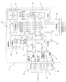
- FIG. 1 shows a functional block diagram of the motor control device of the present embodiment.
- the motor control device 1 includes two safety stop units 10 and 20, a gate drive circuit unit 30, an inverter unit (not shown), an EDM monitoring unit 40, and a device control unit 50. .
- the two safety stop units 10 and 20 mainly include photocouplers 11 and 21, gate buffers 12 and 22, and two NOT gates 13, 14, 23, and 24, respectively.
- Each of the photocouplers 11 and 21 has an input terminal (a set of two on the left side in the figure) and an output terminal (a set of two on the right side in the figure).
- a switching control signal corresponding to the state of the stop input signals HWBB1 and HWBB2 input to the input terminal from the outside of the control device 1 is output from the output terminal. That is, the input state of the stop input signals HWBB1 and HWBB2 input to the input terminal is transmitted to the output terminal while ensuring electrical insulation between the input terminal side and the output terminal side.
- the gate buffers 12 and 22 are internally provided with a plurality of three-state buffers in parallel (not shown in particular), and are connected and disconnected between the inputs and outputs of all the three-state buffers by a switching control signal (hereinafter, referred to as “gate buffers”) (The function of the gate buffers 12 and 22 will be described in detail later with reference to FIG. 2).
- the NOT gates 13, 14, 23, and 24 are connected in series to the switching control signal output from the output terminals of the photocouplers 11 and 21, and are configured as Schmitt triggers for preventing chattering (hysteresis characteristics). It has.
- a switching control signal output from the first NOT gates 13 and 23 as viewed from the photocouplers 11 and 21 is input to a comparative diagnosis unit 80 (to be described later) of the apparatus control unit 50, and is input from the second NOT gates 14 and 24.
- the output switching control signal is input to the switching control input terminals of the gate buffers 12 and 22.
- the L level is input to the first NOT gates 13 and 23 (the NOT gates 13 and 23 are at the H level).
- H level is output to the second NOT gates 14 and 24 (the NOT gates 14 and 24 output L level).
- the two gate buffers 12 and 22 are connected in series with respect to each of six PWM signals output from a PWM control unit to be described later, that is, for each PWM signal, for channel 1 (CH.1).
- the safety stop unit 10 and the safety stop unit 20 for channel 2 (CH.2) are provided in a double manner.
- the gate drive circuit unit 30 receives a PWM signal through the two gate buffers 12 and 22, and an inverter unit (particularly, provided outside the motor control device 1 based on the PWM signal). A motor drive command is output to (not shown).
- the inverter unit converts direct current into alternating current by switching between conduction and interruption of the internal switching element in accordance with the motor drive command, and supplies drive power to a motor (not shown).
- illustration of an inverter part is abbreviate
- the inverter unit is composed of, for example, an IGBT or an IGBT module.
- the inverter unit may include the gate drive circuit unit 30.
- the EDM monitoring unit 40 mainly includes a photocoupler 41 and an AND gate 42.
- each of the two gate buffers 12 and 22 has a function state signal output terminal, and the function state signal output from these function state signal output terminals is input to the AND gate 42.
- the AND gate 42 (logical product circuit) takes the logical product of the two functional state signals and inputs the output to the input terminal of the photocoupler 41.
- the photocoupler 41 is turned on when the output of the AND gate 42 is L level.
- the photocoupler 41 transmits the input state of the signal input to the input terminal to the output terminal and outputs it to the outside of the motor control device 1 while ensuring electrical insulation between the input terminal side and the output terminal side. .
- the apparatus control unit 50 (control unit, means for discriminating abnormality of the gate buffer) mainly includes a PWM control unit 60, a pulse diagnosis unit 70, and a comparison diagnosis unit 80.
- the PWM control unit 80 (PWM generation circuit) generates, for example, a PWM signal for driving and controlling the motor based on a command from a host control device (not shown) provided outside the motor control device 1, for example. Output.
- a host control device not shown
- two PWM signals PU0, NU0, PV0 two in each phase corresponding to the case where the motor to be controlled is a three-phase AC motor (including a rotary type and a direct acting type), NV0, PW0, and NW0 are output.
- the pulse diagnostic unit 70 includes a CPU 71, a GPIO 72, and a level inversion unit 73.
- the CPU 71 inputs the same test signal DPOUT to the diagnostic signal input terminal provided in each of the two gate buffers 12 and 22 via the GPIO 72.
- the test signal DPOUT is a signal that dynamically changes, and is output as a pulse waveform signal that periodically changes in the example of the present embodiment.
- the two gate buffers 12 and 22 are each provided with a diagnostic signal output terminal for outputting diagnostic signals DPIN1 and DPIN2 (signal output from the gate buffer) based on the test signal DPOUT input to the diagnostic signal input terminal.
- the level inversion unit 73 inverts the levels of the diagnostic signals DPIN1 and DPIN2 output from the respective diagnostic signal output terminals, and inputs them to the CPU 71 via the GPIO 72.
- the comparative diagnosis unit 80 (switching control signal branch input unit) includes two NOT gates 81 and 82 and an alarm notification unit 83.
- the switching control signals output from the first NOT gates 13 and 23 in the two safety stop units 10 and 20 are inverted in level by the two NOT gates 81 and 82 of the comparative diagnosis unit 80, respectively, and an alarm is generated.
- the information is input to the notification unit 83.
- the state contents of the two switching control signals BBON1 and BBON2 input to the alarm notification unit 83 are equivalent to the state contents of the switching control signals input to the gate buffers 12 and 22, respectively.
- the two NOT gates 81 and 82 provided in the comparative diagnosis unit 80 also have a Schmitt trigger configuration (hysteresis characteristics).
- the alarm notification unit 83 has two functions.
- the first function is to input the stop input signals HWBB1 and HWBB2 to the safety stop sections 10 and 20 based on the two signals (switching control signals BBON1 and BBON2) input to the alarm notification section 83, respectively.
- This is a function for determining whether or not a failure has occurred in at least one of the photo-operation couplers 11 and 21 (see FIGS. 3 and 4 described later).
- the second function is a function for transmitting and inputting the output signals of the two NOT gates 81 and 82 to the CPU 71 as they are so that the pulse diagnosis unit 70 can determine the occurrence of abnormality in the two gate buffers 12 and 22. is there.
- the gate buffers 12 and 22 include six PWM signal input terminals 91 (PWM signal input units), six PWM signal output terminals 92 (PWM signal output units), and a switching control signal input terminal 93 (switching).
- Signal input unit diagnostic signal input terminal 94 (diagnostic signal input unit), diagnostic signal output terminal 95 (diagnostic signal output unit), functional state signal output terminal 96 (functional state signal output unit), and power supply terminal 97 It has.
- the gate buffers 12 and 22 are provided with six 3-state buffers corresponding to each PWM signal in parallel.
- gate buffers 12 and 22 The main functions of such gate buffers 12 and 22 are to switch the conduction state of each three-state buffer based on the switching control signals BBON1 and BBON2 input to the switching control signal input terminal 93, thereby respectively corresponding PWM. All the conduction states between the signal input terminal 91 and the PWM signal output terminal 92 are switched to the same state.
- the switching control signals BBON1 and BBON2 are at the L level, the PWM signal input terminal 91 and the PWM signal output terminal 92 are electrically connected (that is, the normally-on input photocouplers 11 and 21 are normally turned on and the photocoupler output is output). The state which becomes L level).
- the switching control signals BBON1 and BBON2 are at the H level, the connection between the PWM signal input terminal 91 and the PWM signal output terminal 92 is cut off (that is, the normally-on input photocouplers 11 and 21 are turned off when the normal operation is performed). (The coupler output is at H level). At this time, the PWM signal output terminal 92 is in a high impedance state (so-called active-low configuration).
- auxiliary functions of the gate buffers 12 and 22 include output of diagnostic signals DPIN1 and DPIN2 and a function status signal.
- the conduction state between the diagnostic signal input terminal 94 and the diagnostic signal output terminal 95 is configured to be the same conduction state between the PWM signal input terminal 91 and the PWM output terminal in the normal state. However, when an abnormality occurs in the internal 3-state buffer due to a failure or the like, the diagnostic signal output terminal 95 sets the H level or the L level regardless of the level of the test signal DPOUT input to the diagnostic signal input terminal 94. Only the diagnostic signals DPIN1 and DPIN2 that are maintained constant are output.
- the gate buffers 12 and 22 output the switching control signals BBON1 and BBON2 and a function state signal corresponding to the conduction state between the PWM signal input terminal 91 and the PWM signal output unit terminal 92 from the function state signal output terminal 96.
- the gate buffers 12 and 22 internally determine the occurrence of an abnormality based on the switching control signals BBON1 and BBON2 and the conduction state between the PWM signal input terminal 91 and the PWM signal output terminal 92.
- the function state signal is output at H level.
- the conduction of the PWM signal of the two gate buffers 12 and 22 is switched on and off by the input of the two stop input signals HWBB1 and HWBB2, and the motor power supply drive and the stop thereof are easy. And it has a double STO (Safe Torque OFF) function that switches reliably.
- a single stop operation unit (not shown) composed of, for example, a push button switch or the like outside the apparatus inputs two stop input signals HWBB1 and HWBB2 at H level during normal operation. It is provided in a mullion configuration (that is, a state in which normally-on input photocouplers 11 and 21 are turned on and the photocoupler output is at L level in a normal state).
- the conduction state between the PWM signal input terminal 91 and the PWM signal output terminal 92 is forcibly cut off due to its own failure, or the PWM signal input terminal.
- a functional abnormality occurs such that the output level from the PWM signal output terminal 92 is maintained at the H level or the L level regardless of the input level to 91.
- the safety stop units 10 and 20 may malfunction due to a failure of at least one of the stop operation unit and the photocouplers 11 and 21 described above.
- the motor control device 1 of the present embodiment specifies the cause of the HWBB state by the comparative diagnosis unit 80 and the pulse diagnosis unit 70 separately from the EDM monitoring unit 40.
- the stop operation unit of this example is configured to input two stop input signals HWBB1 and HWBB2 at the same level as a single unit. Therefore, the comparative diagnosis unit 80 can determine the occurrence of a failure in at least one of the stop operation unit and the photocouplers 11 and 21 based on the combination of the contents of the two input switching control signals BBON1 and BBON2. For example, as shown in FIG. 3, when the two switching control signals BBON1 and BBON2 are both at the L level or both are at the H level, the two stop input signals HWBB1 and HWBB2 are both in the ON state or both. Since it is in the OFF state, it can be determined that all of the stop operation unit and the photocouplers 11 and 21 are normal.
- the two switching control signals BBON1 and BBON2 are different between the L level and the H level, the contents of the two stop input signals HWBB1 and HWBB2 are also different from each other. It can be determined that a failure has occurred in at least one of 11 and 21.
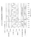
- Fig. 4 shows a time chart of the comparative diagnosis operation when a failure occurs in the stop operation unit.
- the comparative diagnosis unit 80 performs diagnosis in a system cycle of 2 ms.
- one of the two switching control signals BBON1 and BBON2 is in an OFF state (H level in this example, the photocouplers 11 and 21 are in an OFF state, CH.2 in the illustrated example)
- the corresponding gate buffer 12 and 22 are cut off to enter the HWBB state, and “HWBB in operation” is displayed on a display (not shown).
- the comparative diagnosis unit 80 determines the failure of at least one of the stop operation unit and the photocouplers 11 and 21, and displays “stop operation device failure occurrence” on the display while maintaining the HWBB state. At this time, the alarm notification unit stops the operation of the PWM control unit.
- the pulse diagnosis unit 70 also includes the gate buffers 12 and 22 based on the two switching control signals BBON1 and BBON2 input from the comparison diagnosis unit 80 and the two diagnosis signals DPIN1 and DPIN2 input from the level inversion unit 73.
- the occurrence of an abnormality can be determined. For example, as shown in FIG. 5, if the switching control signals BBON1 and BBON2 corresponding to the gate buffers 12 and 22 of one channel are at the L level, it is assumed that the corresponding gate buffers 12 and 22 are conductive. Therefore, it can be determined that the diagnosis signals DPIN1 and DPIN2 corresponding to the same gate buffers 12 and 22 have the same pulse waveform as the test signal DPOUT.
- the switching control signals BBON1 and BBON2 are at the L level, if the corresponding diagnostic signals DPIN1 and DPIN2 maintain the H level or the L level constant, the corresponding gate buffers 12 and 22 are abnormal. It can be determined that it has occurred. If the switching control signals BBON1 and BBON2 are at the H level, it is assumed that the corresponding gate buffers 12 and 22 are cut off, so that the diagnostic signals DPIN1 and DPIN2 corresponding to the same gate buffers 12 and 22 are at the level. The inversion unit 73 maintains the H level constant (the gate buffers 12 and 22 are cut off) (determined as normal). The same applies to the other channel. Since the above determination is a periodic signal having a pulse waveform in which the test signal DPOUT changes dynamically, the pulse diagnosis unit 70 can also be determined dynamically.
- Fig. 6 shows the time chart of the pulse diagnosis operation when the gate buffer is normal.
- the pulse diagnosis unit 70 is in an OFF state (H level in this example, the photocouplers 11 and 21 are in an OFF state, CH.2 in the illustrated example) in either one of the two switching control signals BBON1 and BBON2.
- the corresponding gate buffers 12 and 22 are actively cut off in synchronism with the system cycle to put the motor control device 1 in the HWBB state, and “HWBB is operating” on the display or the like. Is displayed.
- the diagnostic signals DPIN1 and DPIN2 are constantly maintained at the H level (or L level).
- Fig. 7 shows a time chart of the pulse diagnosis operation when a gate buffer error occurs.
- the two switching control signals BBON1 and BBON2 are both in the ON state (L level in this example, the photocouplers 11 and 21 are in the on state), for example, CH.
- the diagnostic signal DPIN2 is kept constant at the H level (or L level).
- the switching control signals BBON1 and BBON2 are not changed, and only the diagnostic signal DPIN2 is changed to be kept constant.
- the corresponding gate buffer 22 is shut off to put the motor control device 1 in the HWBB state.
- the pulse diagnosis unit 70 detects and compares the corresponding switching control signal BBON2 immediately in response to the constant maintenance of the diagnostic signal DPIN2. To do.
- the pulse diagnosis unit 70 maintains the diagnosis signal DPIN2 constant while the corresponding switching control signal BBON2 remains in the ON state (L level in this example, the photocouplers 11 and 21 are in the ON state). It is determined that an abnormality has occurred in the corresponding gate buffer 22, and the name of the gate buffer corresponding to the display ("CH.2 gate buffer") and "abnormality occurrence" are displayed in the next system cycle.
- the CPU stops the operation of the PWM control unit due to the occurrence of an abnormality in one of the gate buffers 22.
- stop operation unit normally on, normally off setting, the number and arrangement of the NOT gates 13, 14, 23, and 24 may be appropriately changed according to the specifications of the gate buffers 12 and 22. 3. The correspondence of the signals in FIG. 5 may be changed accordingly.
- the motor control device 1 includes the device control unit 50 configured to determine the abnormality of the gate buffers 12 and 22 by applying the test signal DPOUT to the gate buffers 12 and 22.
- the occurrence of abnormality in the gate buffers 12 and 22 can be determined, and the gate buffer determined to be abnormal can be specified.
- the apparatus control unit 50 can determine whether an abnormality has occurred in the gate buffers 12 and 22 even when the operator experimentally operates the stop operation unit regardless of whether the motor is being driven or stopped. .
- the device control unit 50 includes a comparative diagnosis unit 80 configured to branch-input switching control signals BBON1 and BBON2 for conducting or blocking the PWM signal with respect to the gate buffers 12 and 22.
- the test signal DPOUT that dynamically changes is output to the gate buffers 12 and 22, and the state of the switching control signals BBON1 and BBON2 and the state of the diagnostic signals DPIN1 and DPIN2 from the gate buffers 12 and 22 are output.
- a pulse diagnostic unit 70 configured to discriminate abnormality of the gate buffers 12 and 22.
- the apparatus control unit 50 causes the pulse diagnosis unit 70 to compare the state of the switching control signals BBON1 and BBON2 of the gate buffers 12 and 22 with the diagnosis signals DPIN1 and DPIN2, thereby generating an abnormality in the gate buffers 12 and 22. Can be determined dynamically, and quick and reliable determination is possible.
- the gate buffers 12 and 22 include a PWM signal input terminal 91 for inputting a PWM signal, a PWM signal output terminal 92 for outputting the PWM signal inputted to the PWM signal input terminal 91 as it is, and a PWM.
- a switching control signal input terminal 93 for inputting switching control signals BBON1 and BBON2 for switching between conduction and blocking between the signal input terminal 91 and the PWM signal output terminal 92, and a PWM signal input terminal based on the switching control signals BBON1 and BBON2.
- the diagnostic signal input terminal 94 and the diagnostic signal output terminal 95 are in the same state as the conduction or cutoff state between 91 and the PWM signal output terminal 92.
- the pulse diagnosis unit 70 receives the switching control signals BBON1 and BBON2 from the comparative diagnosis unit 80 and also inputs the test signal DPOUT to the diagnostic signal input terminal 94, and the state of the switching control signals BBON1 and BBON2 and the diagnostic signal DPIN1.
- the abnormality of the gate buffers 12 and 22 is determined based on the state of DPIN2.
- the diagnostic signals DPIN1 and DPIN2 do not change dynamically and are stably maintained at a certain level (H or L), at least between the PWM signal input terminal 91 and the PWM signal output terminal 92 in the gate buffers 12 and 22. It is possible to determine whether an abnormality has occurred in the conduction state.
- the device control unit 50 compares the switching control signals BBON1 and BBON2 with the diagnostic signals DPIN1 and DPIN2, specifically the contents of the conduction state commanded by the switching control signals BBON1 and BBON2, and the diagnosis.
- the contents of the conduction state indicated by the signals DPIN1 and DPIN2 are different, it can be determined that an abnormality has occurred in the gate buffers 12 and 22 corresponding to the switching control signals BBON1 and BBON2 and the diagnostic signals DPIN1 and DPIN2.
- a double fail-safe mechanism can be configured by providing a plurality of gate buffers 12 and 22 connected in series.
- the motor drive can be stopped more reliably.
- the gate buffers 12 and 22 are connected and disconnected between the corresponding switching control signals BBON1 and BBON2 and the PWM signal input terminal 91 and the PWM signal output terminal 92 in the gate buffers 12 and 22, respectively.
- the motor control device 1 has an AND gate configured to output a logical product of the function state signals output from the function state signal output terminals 96 of the gate buffers 12 and 22. Thereby, regardless of any of the plurality of gate buffers 12 and 22, the change in the function state can be confirmed only by the output of one AND gate. Further, by providing the EDM monitoring unit 40, it is possible to maintain a prescribed signal input format for the host controller and the like.
- the pulse diagnosis unit 70 outputs the test signal DPOUT as a periodic signal.
- the diagnostic signals DPIN1 and DPIN2 can actively reflect the change in conduction and interruption, thereby enabling more reliable and quick detection of interruption. It becomes possible.
- the test signal DPOUT has the same effect as a periodic signal such as a sine wave in addition to the pulse waveform.
- test signal DPOUT is a periodic signal having a pulse waveform. This is suitable for application to a digital circuit.
- One of the signal lines between the two has a level inverting unit 73 configured to invert the signal state contents.
- the level inversion unit 73 If the level inversion unit 73 is not provided, even if a short circuit occurs between the two signal lines, the waveforms of the respective signals coincide with each other, so that the occurrence of the short circuit cannot be detected. However, when a short circuit occurs because the two signals determine each other, the determination signal cannot maintain a prescribed pulse waveform, and a short circuit can be detected. Note that when the test signal DPOUT is a pulse waveform, the logic value may be inverted, but when the test signal DPOUT is a sine wave, the polarity is inverted.
- the configuration in which the gate buffers 12 and 22 are provided in double by single-axis control for controlling only one motor is shown, but the present invention is not limited to this.
- two gate buffers are provided in two-axis control for controlling two motors
- two gate buffers connected in series are provided corresponding to each axis as shown in FIG. (Buffers 12, 22, 112, 122)
- the two safety stop units 10, 20, the EDM monitoring unit 40, and the input of the test signal DPOUT are provided in parallel to each set of gate buffers 12, 22, 112, 122. That's fine.
- only one gate buffer may be provided corresponding to one axis.
Priority Applications (4)
| Application Number | Priority Date | Filing Date | Title |
|---|---|---|---|
| EP13896412.7A EP3065290B1 (de) | 2013-10-30 | 2013-10-30 | Motorsteuerungsvorrichtung |
| JP2015544698A JP6150222B2 (ja) | 2013-10-30 | 2013-10-30 | モータ制御装置 |
| PCT/JP2013/079434 WO2015063892A1 (ja) | 2013-10-30 | 2013-10-30 | モータ制御装置 |
| US15/138,222 US9941823B2 (en) | 2013-10-30 | 2016-04-26 | Motor control device |
Applications Claiming Priority (1)
| Application Number | Priority Date | Filing Date | Title |
|---|---|---|---|
| PCT/JP2013/079434 WO2015063892A1 (ja) | 2013-10-30 | 2013-10-30 | モータ制御装置 |
Related Child Applications (1)
| Application Number | Title | Priority Date | Filing Date |
|---|---|---|---|
| US15/138,222 Continuation US9941823B2 (en) | 2013-10-30 | 2016-04-26 | Motor control device |
Publications (1)
| Publication Number | Publication Date |
|---|---|
| WO2015063892A1 true WO2015063892A1 (ja) | 2015-05-07 |
Family
ID=53003540
Family Applications (1)
| Application Number | Title | Priority Date | Filing Date |
|---|---|---|---|
| PCT/JP2013/079434 WO2015063892A1 (ja) | 2013-10-30 | 2013-10-30 | モータ制御装置 |
Country Status (4)
| Country | Link |
|---|---|
| US (1) | US9941823B2 (de) |
| EP (1) | EP3065290B1 (de) |
| JP (1) | JP6150222B2 (de) |
| WO (1) | WO2015063892A1 (de) |
Cited By (3)
| Publication number | Priority date | Publication date | Assignee | Title |
|---|---|---|---|---|
| CN106842004A (zh) * | 2015-12-07 | 2017-06-13 | Abb技术有限公司 | 用于测试电力驱动器中的安全转矩关断电路的方法和装置 |
| JP2019161883A (ja) * | 2018-03-14 | 2019-09-19 | 富士電機株式会社 | 電力変換装置 |
| WO2019239753A1 (ja) * | 2018-06-15 | 2019-12-19 | パナソニックIpマネジメント株式会社 | 遮断回路診断装置 |
Families Citing this family (9)
| Publication number | Priority date | Publication date | Assignee | Title |
|---|---|---|---|---|
| AT516568B1 (de) | 2014-11-21 | 2017-03-15 | Bernecker + Rainer Industrie-Elektronik Ges M B H | Vorrichtung und ein Verfahren zur sicheren Ansteuerung eines Halbleiterschalters eines Wechselrichters |
| JP7054849B2 (ja) * | 2017-05-31 | 2022-04-15 | パナソニックIpマネジメント株式会社 | 診断装置 |
| KR20190136233A (ko) * | 2018-05-30 | 2019-12-10 | 엘에스산전 주식회사 | 인버터 보호장치 |
| DE102019130403A1 (de) * | 2019-11-11 | 2021-05-12 | Hirschmann Automation And Control Gmbh | Logikgatter sowie ein Logikgattersystem |
| CN111522226B (zh) * | 2020-05-20 | 2022-06-28 | 中国科学院光电技术研究所 | 针对伺服转台的多目标优化高型pid最优控制器设计方法 |
| DE102020121253A1 (de) * | 2020-08-12 | 2022-02-17 | Vacon Oy | Drehzahlvariable Ansteuerung zum Ansteuern eines Elektromotors und Verfahren zur Diagnose der Ansteuerung |
| US11502629B2 (en) * | 2020-12-30 | 2022-11-15 | Texas Instruments Incorporated | Hardware based motor drive controller |
| DE102021211208A1 (de) * | 2021-10-05 | 2023-04-06 | Robert Bosch Gesellschaft mit beschränkter Haftung | Steuervorrichtung und Verfahren zum Betreiben eines Elektromotors, insbesondere eines Lenksystems |
| US20230327669A1 (en) * | 2022-04-07 | 2023-10-12 | Sehat Sutardja | Noise tolerant buffer |
Citations (4)
| Publication number | Priority date | Publication date | Assignee | Title |
|---|---|---|---|---|
| JPS6156983A (ja) * | 1984-08-27 | 1986-03-22 | Toshiba Corp | 半導体装置およびそのテスト方法 |
| JP2010104188A (ja) | 2008-10-27 | 2010-05-06 | Panasonic Corp | 内転型電動機の固定子鉄心およびそれを用いたモールドモータ |
| JP2010104187A (ja) * | 2008-10-27 | 2010-05-06 | Yaskawa Electric Corp | 安全停止回路を備えたモータ制御装置 |
| JP2013223363A (ja) * | 2012-04-18 | 2013-10-28 | Mitsubishi Electric Corp | 電動機駆動制御装置 |
Family Cites Families (4)
| Publication number | Priority date | Publication date | Assignee | Title |
|---|---|---|---|---|
| JPH07181227A (ja) * | 1993-12-22 | 1995-07-21 | Kawasaki Steel Corp | 集積回路 |
| DE102004043877B4 (de) * | 2004-09-10 | 2012-03-22 | Siemens Ag | Antriebssteuereinrichtung für einen selbstgeführten Stromrichter |
| US8397112B2 (en) * | 2010-08-06 | 2013-03-12 | Texas Instruments Incorporated | Test chain testability in a system for testing tri-state functionality |
| US8976551B2 (en) * | 2010-12-07 | 2015-03-10 | Hitachi Automotive Systems, Ltd. | Power converter |
-
2013
- 2013-10-30 WO PCT/JP2013/079434 patent/WO2015063892A1/ja active Application Filing
- 2013-10-30 JP JP2015544698A patent/JP6150222B2/ja active Active
- 2013-10-30 EP EP13896412.7A patent/EP3065290B1/de active Active
-
2016
- 2016-04-26 US US15/138,222 patent/US9941823B2/en active Active
Patent Citations (4)
| Publication number | Priority date | Publication date | Assignee | Title |
|---|---|---|---|---|
| JPS6156983A (ja) * | 1984-08-27 | 1986-03-22 | Toshiba Corp | 半導体装置およびそのテスト方法 |
| JP2010104188A (ja) | 2008-10-27 | 2010-05-06 | Panasonic Corp | 内転型電動機の固定子鉄心およびそれを用いたモールドモータ |
| JP2010104187A (ja) * | 2008-10-27 | 2010-05-06 | Yaskawa Electric Corp | 安全停止回路を備えたモータ制御装置 |
| JP2013223363A (ja) * | 2012-04-18 | 2013-10-28 | Mitsubishi Electric Corp | 電動機駆動制御装置 |
Cited By (6)
| Publication number | Priority date | Publication date | Assignee | Title |
|---|---|---|---|---|
| CN106842004A (zh) * | 2015-12-07 | 2017-06-13 | Abb技术有限公司 | 用于测试电力驱动器中的安全转矩关断电路的方法和装置 |
| JP2019161883A (ja) * | 2018-03-14 | 2019-09-19 | 富士電機株式会社 | 電力変換装置 |
| JP7047499B2 (ja) | 2018-03-14 | 2022-04-05 | 富士電機株式会社 | 電力変換装置 |
| WO2019239753A1 (ja) * | 2018-06-15 | 2019-12-19 | パナソニックIpマネジメント株式会社 | 遮断回路診断装置 |
| US11735904B2 (en) | 2018-06-15 | 2023-08-22 | Panasonic Intellectual Property Management Co., Ltd. | Cut-off circuit diagnostic device |
| JP7398620B2 (ja) | 2018-06-15 | 2023-12-15 | パナソニックIpマネジメント株式会社 | 遮断回路診断装置 |
Also Published As
| Publication number | Publication date |
|---|---|
| US9941823B2 (en) | 2018-04-10 |
| EP3065290B1 (de) | 2018-12-12 |
| JP6150222B2 (ja) | 2017-06-21 |
| JPWO2015063892A1 (ja) | 2017-03-09 |
| EP3065290A1 (de) | 2016-09-07 |
| US20160241174A1 (en) | 2016-08-18 |
| EP3065290A4 (de) | 2017-05-17 |
Similar Documents
| Publication | Publication Date | Title |
|---|---|---|
| JP6150222B2 (ja) | モータ制御装置 | |
| US8476860B2 (en) | Electric power converter | |
| JP5370724B2 (ja) | 安全停止回路を備えたモータ制御装置 | |
| WO2010044243A1 (ja) | モータ制御装置 | |
| JP6107745B2 (ja) | 電力変換装置、及び、電力変換装置の異常診断方法 | |
| JP2017169336A (ja) | モータ制御装置 | |
| JP7054849B2 (ja) | 診断装置 | |
| JPWO2008132975A1 (ja) | 電力変換装置 | |
| JP7398620B2 (ja) | 遮断回路診断装置 | |
| WO2018155510A1 (ja) | モータ制御装置 | |
| EP3220539B1 (de) | Motorsteuerung | |
| JP2007028752A (ja) | エレベータ電動機制御装置 | |
| JP2018136712A (ja) | モータ制御装置 | |
| JP2013247693A (ja) | 電動機駆動用電力変換装置 | |
| CN111162697A (zh) | 马达控制装置 | |
| JP6120723B2 (ja) | 制御回路、制御回路の短絡故障検知方法、転轍制御回路の短絡故障検知方法および鉄道信号用連動制御システム | |
| CN107851974B (zh) | 断路控制方法和使用它的电力转换装置 | |
| JP4575876B2 (ja) | インバータ装置及びインバータシステム | |
| WO2018155509A1 (ja) | モータ制御装置 | |
| JP2018195128A (ja) | 診断装置 | |
| JP6332496B2 (ja) | モータ制御装置 | |
| JP6572300B2 (ja) | 制御装置及び電力変換装置 |
Legal Events
| Date | Code | Title | Description |
|---|---|---|---|
| 121 | Ep: the epo has been informed by wipo that ep was designated in this application |
Ref document number: 13896412 Country of ref document: EP Kind code of ref document: A1 |
|
| ENP | Entry into the national phase |
Ref document number: 2015544698 Country of ref document: JP Kind code of ref document: A |
|
| NENP | Non-entry into the national phase |
Ref country code: DE |
|
| REEP | Request for entry into the european phase |
Ref document number: 2013896412 Country of ref document: EP |
|
| WWE | Wipo information: entry into national phase |
Ref document number: 2013896412 Country of ref document: EP |