WO2015056368A1 - 移載装置および移載方法 - Google Patents
移載装置および移載方法 Download PDFInfo
- Publication number
- WO2015056368A1 WO2015056368A1 PCT/JP2014/002506 JP2014002506W WO2015056368A1 WO 2015056368 A1 WO2015056368 A1 WO 2015056368A1 JP 2014002506 W JP2014002506 W JP 2014002506W WO 2015056368 A1 WO2015056368 A1 WO 2015056368A1
- Authority
- WO
- WIPO (PCT)
- Prior art keywords
- substrate
- flat plate
- receiving jig
- driver
- magnet
- Prior art date
- Legal status (The legal status is an assumption and is not a legal conclusion. Google has not performed a legal analysis and makes no representation as to the accuracy of the status listed.)
- Ceased
Links
Images






Classifications
-
- B—PERFORMING OPERATIONS; TRANSPORTING
- B65—CONVEYING; PACKING; STORING; HANDLING THIN OR FILAMENTARY MATERIAL
- B65G—TRANSPORT OR STORAGE DEVICES, e.g. CONVEYORS FOR LOADING OR TIPPING, SHOP CONVEYOR SYSTEMS OR PNEUMATIC TUBE CONVEYORS
- B65G49/00—Conveying systems characterised by their application for specified purposes not otherwise provided for
- B65G49/05—Conveying systems characterised by their application for specified purposes not otherwise provided for for fragile or damageable materials or articles
- B65G49/06—Conveying systems characterised by their application for specified purposes not otherwise provided for for fragile or damageable materials or articles for fragile sheets, e.g. glass
- B65G49/061—Lifting, gripping, or carrying means, for one or more sheets forming independent means of transport, e.g. suction cups, transport frames
-
- G—PHYSICS
- G02—OPTICS
- G02F—OPTICAL DEVICES OR ARRANGEMENTS FOR THE CONTROL OF LIGHT BY MODIFICATION OF THE OPTICAL PROPERTIES OF THE MEDIA OF THE ELEMENTS INVOLVED THEREIN; NON-LINEAR OPTICS; FREQUENCY-CHANGING OF LIGHT; OPTICAL LOGIC ELEMENTS; OPTICAL ANALOGUE/DIGITAL CONVERTERS
- G02F1/00—Devices or arrangements for the control of the intensity, colour, phase, polarisation or direction of light arriving from an independent light source, e.g. switching, gating or modulating; Non-linear optics
- G02F1/01—Devices or arrangements for the control of the intensity, colour, phase, polarisation or direction of light arriving from an independent light source, e.g. switching, gating or modulating; Non-linear optics for the control of the intensity, phase, polarisation or colour
- G02F1/13—Devices or arrangements for the control of the intensity, colour, phase, polarisation or direction of light arriving from an independent light source, e.g. switching, gating or modulating; Non-linear optics for the control of the intensity, phase, polarisation or colour based on liquid crystals, e.g. single liquid crystal display cells
- G02F1/1303—Apparatus specially adapted to the manufacture of LCDs
-
- B—PERFORMING OPERATIONS; TRANSPORTING
- B65—CONVEYING; PACKING; STORING; HANDLING THIN OR FILAMENTARY MATERIAL
- B65G—TRANSPORT OR STORAGE DEVICES, e.g. CONVEYORS FOR LOADING OR TIPPING, SHOP CONVEYOR SYSTEMS OR PNEUMATIC TUBE CONVEYORS
- B65G2249/00—Aspects relating to conveying systems for the manufacture of fragile sheets
- B65G2249/04—Arrangements of vacuum systems or suction cups
- B65G2249/045—Details of suction cups suction cups
Definitions
- the present disclosure relates to a transfer device used when transferring a substrate, and a transfer method using the transfer device.
- Patent Document 1 discloses a substrate holding and fixing jig for holding and fixing a substrate for transporting the substrate to another place.
- the substrate holding and fixing jig includes a suction cup, a passage for sending air into the suction cup, and an opening / closing valve for opening and closing the atmosphere in the passage. Thereby, the substrate can be held and fixed by vacuum suction.
- This disclosure is intended to provide a transfer apparatus effective for transferring a substrate independent of dimensions and shapes, and a transfer method using the same.
- a transfer device is a transfer device used for transferring a substrate, one end of which is connected to a string-like body and suspended at a predetermined height, and the substrate A flat plate portion that supports the substrate by contacting at least a part of the lower surface, and a hole formed in the flat plate portion that can be inserted through a hole having a predetermined size.
- a substrate receiving jig having a protruding portion, and the magnet holds the substrate receiving jig at a predetermined height by adsorbing the tip of the protruding portion with a magnetic force.
- FIG. 1 is a diagram schematically showing a display panel with a driver substrate.
- FIG. 2A is a diagram schematically illustrating a method of holding a display panel with a driver substrate using vacuum suction in order to transfer the display panel.
- FIG. 2B is a side view of FIG. 2A.
- FIG. 3 is a diagram schematically illustrating the configuration of the transfer apparatus according to the first embodiment.
- FIG. 4 is a diagram illustrating another example of the configuration of the magnet according to the first embodiment.
- FIG. 5A is a diagram illustrating an example of a shape when the transfer apparatus according to Embodiment 1 is viewed from above.
- FIG. 5B is a diagram showing another example of the shape when the transfer device according to Embodiment 1 is viewed from above.
- FIG. 5A is a diagram illustrating an example of a shape when the transfer apparatus according to Embodiment 1 is viewed from above.
- FIG. 5B is a diagram showing another example of the shape when the transfer device according to Embod
- FIG. 7A is a diagram schematically illustrating a method of holding the display panel with a driver substrate using the transfer apparatus according to the first embodiment.
- FIG. 7B is a side view of FIG. 7A.
- FIG. 8 is a diagram schematically showing the configuration of the substrate receiving jig according to the second embodiment.
- FIG. 9 is a diagram schematically illustrating another example of the configuration of the substrate receiving jig according to the second embodiment.
- FIG. 10 is a diagram schematically showing the configuration of the substrate receiving jig according to the third embodiment.
- FIG. 11 is a diagram schematically illustrating a usage example of the substrate receiving jig according to the third embodiment.
- FIG. 12 is a diagram schematically illustrating another example of the configuration of the substrate receiving jig according to the third embodiment.
- the substrate may be described as a driver substrate connected to the display panel by flexible wiring.
- the board is not limited to the driver board.
- FIG. 1 is a diagram schematically showing a display panel with a driver board.
- the display panel 100 with a driver substrate includes a display panel 101, one or more driver substrates 102, and a flexible substrate 103.
- the display panel 101 is, for example, a liquid crystal display panel, an organic EL (Electro Luminescence) panel, or a plasma display panel, and is assembled in a display device to display an image.
- a liquid crystal display panel for example, an organic EL (Electro Luminescence) panel, or a plasma display panel, and is assembled in a display device to display an image.
- organic EL Electro Luminescence
- the driver board 102 includes a mounting hole 104, and a driver circuit for supplying a display signal to the display panel 101 is mounted.
- the driver substrate 102 is, for example, a printed circuit board (PCB: Printed Circuit Board), but may be formed as a rigid portion of a rigid flexible substrate.
- the driver circuit is configured by mounting a plurality of components on the surface (component mounting surface) of the driver substrate 102 together with wiring.
- the mounting hole 104 is a hole that the driver board 102 has and has a predetermined size.
- the attachment hole 104 is a through-hole to which a fastening member such as a screw having a diameter of about 10 mm is attached.
- the mounting holes 104 are holes that are necessary when the display panel 100 with a driver substrate is assembled to a display device, and are necessarily provided.
- the flexible substrate 103 is mounted with flexible wiring, and connects the display panel 101 and the driver substrate 102 physically and electrically.
- the flexible substrate is, for example, a flexible printed circuit (FPC), but may be formed as a flexible portion of a rigid flexible substrate.
- FPC flexible printed circuit
- the display panel 100 with a driver board is first manufactured in a clean room, transported outside the clean room, and then assembled into a display device.
- the mounting table on which the display panel 100 with a driver substrate is mounted is different between inside and outside the clean room. For this reason, it is necessary to transfer the display panel 100 with a driver substrate.
- FIG. 2A is a diagram schematically showing a method of holding a display panel with a driver substrate using vacuum suction in order to transfer the display panel.
- FIG. 2B is a side view of FIG. 2A. Elements similar to those in FIG. 1 are denoted by the same reference numerals, and detailed description thereof is omitted.
- the display panel 101 with the driver substrate is transferred by holding the display panel 101 by vacuum suction with the suction pad 905 and holding the driver substrate 102 with vacuum suction by the suction pad 906. Can be listed.
- the suction pad 905 needs to be vacuum-sucked while avoiding a plurality of components (component mounting positions) mounted on the driver board 102.
- the driver board 102 has a restriction on the position where it can be sucked (sucking place).
- the component mounting position is also changed, so the suction location must also be changed.
- a plurality of components and wirings mounted on the driver substrate 102 are increased in density, there may be a case where there is no suction location.
- FIG. 3 is a diagram schematically illustrating the configuration of the transfer apparatus according to the first embodiment.
- FIG. 4 is a diagram illustrating another example of the configuration of the magnet according to the first embodiment.
- FIG. 5A is a diagram illustrating an example of a shape when the transfer apparatus according to Embodiment 1 is viewed from above.
- FIG. 5B is a diagram showing another example of the shape when the transfer device according to Embodiment 1 is viewed from above.
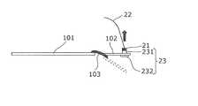
- the transfer device 20 is a transfer device used to transfer the driver substrate 102, and includes a magnet 21 connected to the string-like body 22 and a substrate receiving jig 23. .
- the substrate receiving jig 23 has a protruding portion 231 and a flat plate portion 232.
- the protruding portion 231 is formed in the flat plate portion 232 and is formed so as to be able to be inserted through the mounting hole 104 which is a hole of the driver board 102 and has a predetermined size.
- the protrusion 231 is a metal that is adsorbed by magnetic force, and is, for example, iron, cobalt, nickel, or an alloy containing these.
- the flat plate portion 232 supports the driver board 102 by contacting at least a part of the lower surface of the driver board 102.
- the flat plate portion 232 only needs to be a material intended for weight reduction, and examples thereof include aluminum, copper iron, and an acrylic resin.
- the magnet 21 is connected at one end to the string 22 and suspended at a predetermined height.
- the magnet 21 holds the substrate receiving jig 23 at a predetermined height by attracting the tip of the protruding portion 231 with a magnetic force.
- the magnet 21 is typically composed of a permanent magnet, but may be composed of an electromagnet.
- One end of the magnet 21 may be directly connected to the string-like body 22 by welding or the like, but the string-like body 22 is passed through the connecting member 211 formed on the magnet 21 as shown in FIG. It may be connected by binding.
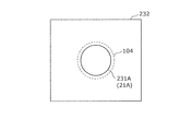
- the shape when the protrusion 231 and the magnet 21 are viewed from above is an ellipse smaller than the mounting hole 104 as shown in FIG. 5A, for example. Thereby, the protrusion 231 can be easily inserted into the mounting hole 104.
- the shape when the protrusion 231 and the magnet 21 are viewed from above may be a circle smaller than the mounting hole 104, such as a circle having a diameter of about 8 mm, for example, as shown in FIG. 5B.
- the shape is arbitrary as long as it can be smoothly inserted into the mounting hole 104 without hindrance and the horizontal displacement of the driver board 102 can be suppressed through the mounting hole 104.
- the string-like body 22 is composed of, for example, a rope, a cable, a metal wire, etc., from which static electricity is prevented, and has a certain length.
- One end of the string-like body 22 is connected to the magnet 21 and the other end is fixed at a constant height, whereby the magnet 21 can be suspended to a predetermined height.
- the predetermined height is, for example, a height at which the display panel 101 is held.
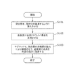
- FIG. 6 is a flowchart for explaining the transfer method of the present disclosure.
- FIG. 7A is a diagram schematically illustrating a method of holding the display panel with a driver substrate using the transfer apparatus according to the first embodiment.
- FIG. 7B is a side view of FIG. 7A. Elements similar to those in FIGS. 1, 2A, and 2B are denoted by the same reference numerals, and detailed description thereof is omitted.
- the protruding portion 231 of the board receiving jig 23 is inserted into the mounting hole 104 so as to penetrate the mounting hole 104 of the driver board 102 (S101).
- the driver board 102 is supported by the board receiving jig 23 by bringing the flat plate portion 232 of the board receiving jig 23 into contact with at least a part of the lower surface of the driver board 102 (S102).
- each of the plurality of magnets 21 is caused to attract the tip of the protruding portion 231 of the substrate receiving jig 23 by magnetic force, so that the substrate receiving jig 23 is brought to a predetermined height as shown in FIG. 7B, for example. Hold (S103).
- each of the plurality of magnets 21 is held at a predetermined height by one end being connected to the string-like body 22.
- each of the string-like bodies 22 can be held at a predetermined height by fixing multiple ends at a certain height and connecting one end to one end of the magnet 21.
- the driver substrate 102 of the display panel 100 with a driver substrate can be held. Can do.
- the display panel 101 is held at a predetermined height by another method such as vacuum suction without using the transfer device 20 as shown in FIG. 7A, for example. In this way, the display panel 100 with a driver substrate held by using the transfer device 20 can be held at substantially the same height as the display panel 101.
- the display panel 101 is vacuum-sucked and held by the suction pad 905 and the driver substrate 102 is sucked and held by the transfer device 20 by magnetic force.
- the display panel 100 with a driver substrate can be transferred while being held at substantially the same height as the display panel 101.
- the display panel 101 and the driver substrate 102 may be held at the same time in order to prevent the driver substrate 102 from being bent.
- the magnet 21 is free to move, and the substrate receiving jig 23 (particularly the flat plate portion 232) can be easily formed in accordance with the driver substrate, so that it is possible to cope with the size and shape of the driver substrate at a low cost.
- the transfer device 20 of the present embodiment the transfer device can be used even if the component placement of the driver substrate 102 is changed due to the size change of the display panel 101. Just increasing the number of 20 can cope.
- the magnet 21 since the magnet 21 is used, it is very easy to attach and detach the string-like body 22 and the substrate receiving jig 23, and the workability is greatly improved.
- FIG. 8 is a diagram schematically showing the configuration of the substrate receiving jig according to the second embodiment. Elements similar to those in FIG. 3 are denoted by the same reference numerals, and detailed description thereof is omitted.
- the substrate receiving jig 23 ⁇ / b> A includes a plurality of flat plate portions 232, a plurality of protruding portions 231, and a connecting portion 233.
- the substrate receiving jig 23A has two flat plate portions 232 as shown in FIG.
- the protruding portion 231 is formed in each of the plurality of flat plate portions 232 and is formed so as to be insertable through the mounting hole 104.
- one protrusion 231 is formed on each of the two flat plate portions 232 as shown in FIG.
- the flat plate portion 232 supports the driver board 102 by contacting at least a part of the lower surface of the driver board 102.
- the connecting portion 233 maintains the plurality of flat plate portions 232 on a substantially flat surface and connects one end portions of the plurality of flat plate portions 232 to each other.
- the connecting portion 233 maintains the two flat plate portions 232 on a substantially flat surface and connects one ends of the two flat plate portions 232 together.
- the connection part 233 should just be a material aiming at weight reduction, for example, aluminum, copper iron, an acrylic resin etc. can be mentioned.
- the substrate receiving jig 23 ⁇ / b> A configured as described above is held at a predetermined height by the magnet 21 by adsorbing the tip ends of the projecting portions 231 formed on the two flat plate portions 232 with a magnetic force.
- the plurality of flat plate portions 232 may be constituted by three.
- FIG. 9 is a diagram schematically illustrating another example of the configuration of the substrate receiving jig according to the second embodiment.
- symbol is attached
- the substrate receiving jig 23B shown in FIG. 9 has three flat plate portions 232, a plurality of protruding portions 231 and a connecting portion 233.
- the connecting portion 233 ⁇ / b> A maintains the three flat plate portions 232 on a substantially flat surface and connects one end portions of the three flat plate portions 232 together.
- the substrate receiving jig 23B is held at a predetermined height by the tips of the protrusions 231 formed on the three flat plate portions 232 by the plurality of magnets 21, respectively.
- one end of each magnet 21 is connected to the string-like body 22 and is suspended to a predetermined height.
- FIG. 10 is a diagram schematically showing the configuration of the substrate receiving jig according to the third embodiment. Elements similar to those in FIGS. 3 and 8 are denoted by the same reference numerals, and detailed description thereof is omitted.
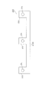
- the substrate receiving jig 23 ⁇ / b> C includes a plurality of flat plate portions 232, a plurality of protruding portions 231, and a connecting portion 233.
- the substrate receiving jig 23C has two flat plate portions 232 and two protruding portions 231 (protruding portions 231A and 231B) on each of the flat plate portions 232 as shown in FIG.
- the protruding portions 231 ⁇ / b> A and 231 ⁇ / b> B are formed on the two flat plate portions 232, respectively, so that they can be inserted so as to penetrate the mounting hole 104.
- the protruding portion 231A is an example of a first protruding portion of the two protruding portions, and is inserted into the mounting hole 104 so as to penetrate the mounting hole 104 of the driver board 102.
- the protruding portion 231B is an example of a second protruding portion of the two protruding portions, and is formed closer to one end of the flat plate portion 232 than the protruding portion 231A.
- one tip of the protrusions 231A and 231B is attracted by the magnetic force of the magnet 21, whereas the magnet 21 is not attracted by the other tip.
- FIG. 11 is a diagram schematically illustrating a usage example of the substrate receiving jig according to the third embodiment.
- symbol is attached
- each of the magnets 21 is configured so that the tip of the protrusion 231B and the tip of the protrusion 231A formed on the one end side of the flat plate portion 232 from the protrusion 231A alternately for each of the one or more flat plates 232, Adsorbed by magnetic force.
- each of the magnets 21 can hold the substrate receiving jig 23C at a predetermined height while preventing the connecting portion 233 from bending and twisting.
- the substrate receiving jig 23 is attached to the mounting hole 104 of the driver substrate 102, and the substrate receiving jig 23 is held by the magnet 21, thereby holding the substrate receiving jig 23C at a predetermined height. can do.
- the substrate receiving jig 23C is attached to the mounting hole 104 of the driver substrate 102, and the two protruding portions 231 of the substrate receiving jig 23 are alternately held by the magnets 21 for each flat plate portion 232.
- the bending and twisting of the connecting portion 233 of the substrate receiving jig 23 can be prevented, and the driver substrate 102 can be held substantially in parallel.
- the magnet 21 is free to move, and the substrate receiving jig 23 (particularly the flat plate portion 232) can be easily formed in accordance with the driver substrate, so that it is possible to cope with the size and shape of the driver substrate at a low cost. Further, since the magnet 21 is used, the attachment and detachment between the string-like body 22 and the substrate receiving jig 23 becomes very easy, so that the workability is greatly improved.
- the plurality of flat plate portions 232 may be configured of three. Hereinafter, this case will be described.
- FIG. 12 is a diagram schematically illustrating another example of the configuration of the substrate receiving jig according to the third embodiment.
- symbol is attached
- the substrate receiving jig 23D shown in FIG. 12 has three flat plate portions 232, a plurality of protruding portions 231 and a connecting portion 233.
- the substrate receiving jig 23D has three flat plate portions 232 and two protruding portions 231 (protruding portions 231A and 231B) on each of the flat plate portions 232 as shown in FIG.
- the connecting portion 233B maintains the three flat plate portions 232 on a substantially flat surface, and connects one end portions of the three flat plate portions 232 to each other.
- the substrate receiving jig 23D has a predetermined height by attracting one of the protrusions 231A and 231B formed on each of the three flat plate portions 232 by a magnetic force by each of the plurality of magnets 21. Is held. That is, each of the magnets 21 is configured so that the leading end of the protruding portion 231B and the leading end of the protruding portion 231A formed on the one end side of the flat plate portion 232 from the protruding portion 231A alternately for each of the plurality of flat plate portions 232. Adsorb at.
- each of the magnets 21 can hold the substrate receiving jig 23D at a predetermined height while preventing the connecting portion 233 from bending and twisting.
- Embodiments 1 to 3 As described above, Embodiments 1 to 3 have been described as examples of the technology in the present disclosure. For this purpose, the accompanying drawings and detailed description are provided.
- the shape when viewed from above the flat plate portion, it is illustrated as a quadrangle, but the shape is not limited thereto, and may be an ellipse, a circle, or a polygon. If the driver substrate can be supported, the shape is not limited to a quadrangle.
- the substrate is described as being a driver substrate connected to the display panel by flexible wiring, but is not limited thereto.
- a driver board mounted on the display panel may be used, or a board other than the driver board may be used.
- the type of the substrate is not limited as long as the mounting hole having a predetermined size according to the standard or specification can be used.
- the case where the driver board is attached to the periphery of the display panel is described as an example, but the present invention is not limited to this.
- the driver board may be connected to only one side of the display panel. That is, the number of driver boards to be attached is not limited.
- the present disclosure can be applied to a transfer device effective for holding a substrate independent of dimensions and shapes and a transfer method using the transfer device.
- the present disclosure can be applied to a transfer device for holding a driver board connected to a display panel, a transfer facility using the transfer device, and the like.
- Transfer device 21 Magnet 22 String-like body 23, 23A, 23B, 23C, 23D Substrate receiving jig 100 Display panel with driver substrate 101 Display panel 102 Driver substrate 103 Flexible substrate 104 Mounting hole 211 Connecting member 231, 231A, 231B Projection Part 232 Flat part 233, 233A, 233B Connecting part 905, 906 Suction pad
Landscapes
- Physics & Mathematics (AREA)
- Nonlinear Science (AREA)
- Engineering & Computer Science (AREA)
- Manufacturing & Machinery (AREA)
- Chemical & Material Sciences (AREA)
- Crystallography & Structural Chemistry (AREA)
- General Physics & Mathematics (AREA)
- Optics & Photonics (AREA)
- Devices For Indicating Variable Information By Combining Individual Elements (AREA)
- Electroluminescent Light Sources (AREA)
Abstract
本開示の移載装置等は、一端が紐状体(22)に連結され、所定の高さに吊り下げられるマグネット(21)と、ドライバ基板(102)の下面の少なくとも一部に当接することでドライバ基板(102)を支持する平板部(232)と、平板部(232)に形成され、ドライバ基板(102)が有する穴であって予め定められた大きさの取付穴(104)を貫通するように挿入可能な突出部(231)とを有する基板受け治具(23)と、を備え、マグネット(21)は、突出部(231)の先端部を磁力で吸着することで、基板受け治具(23)を所定の高さに保持する。
Description
本開示は、基板を移載する際に用いる移載装置、およびそれを用いた移載方法に関する。
特許文献1は、基板を他の場所に搬送するための基板を保持固定する基板保持固定治具を開示する。この基板保持固定治具は、吸盤と、該吸盤内に大気を送り込む通路および該通路内の大気を開閉するための開閉弁とを備える。これにより、基板を真空吸着により保持固定することができる。
本開示は、寸法および形状に依存しない基板移載に有効な移載装置、およびそれを用いた移載方法を提供することを目的とする。
本開示の一態様に係る移載装置は、基板を移載するために用いる移載装置であって、一端が紐状体に連結され、所定の高さに吊り下げられるマグネットと、前記基板の下面の少なくとも一部に当接することで前記基板を支持する平板部と、前記平板部に形成され、前記基板が有する穴であって予め定められた大きさの穴を貫通するように挿入可能な突出部とを有する基板受け治具と、を備え、前記マグネットは、前記突出部の先端部を磁力で吸着することで、前記基板受け治具を所定の高さに保持する。
本開示によれば、寸法および形状に依存しない基板移載に有効な移載装置、およびそれを用いた移載方法を提供することができる。
以下、適宜図面を参照しながら、本発明の実施の形態を詳細に説明する。但し、必要以上に詳細な説明は省略する場合がある。例えば、既によく知られた事項の詳細説明や実質的に同一の構成に対する重複説明を省略する場合がある。これは、以下の説明が不必要に冗長になるのを避け、当業者の理解を容易にするためである。
なお、発明者(ら)は、当業者が本開示を十分に理解するために添付図面および以下の説明を提供するのであって、これらによって請求の範囲に記載の主題を限定することを意図するものではない。
(実施の形態1)
[基板の構成]
以下においては、基板を、表示パネルにフレキシブル配線で接続されているドライバ基板として説明する場合がある。もちろん、基板はドライバ基板に限るものではない。
[基板の構成]
以下においては、基板を、表示パネルにフレキシブル配線で接続されているドライバ基板として説明する場合がある。もちろん、基板はドライバ基板に限るものではない。
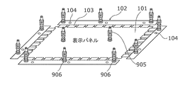
図1は、ドライバ基板付き表示パネルを模式的に示す図である。
ドライバ基板付き表示パネル100は、表示パネル101と、1以上のドライバ基板102と、フレキシブル基板103とを備える。
表示パネル101は、例えば液晶表示パネル、有機EL(Electro Luminescence)パネル、またはプラズマディスプレイパネルであり、表示装置に組み立てられて映像を表示する。
ドライバ基板102は、取付穴104を備え、表示パネル101に表示用の信号を供給するためのドライバ回路が実装されている。ここで、ドライバ基板102は、例えばプリント基板(PCB:Printed Circuit Board)であるが、リジッドフレキシブル基板のリジッド部として形成されているとしてもよい。また、ドライバ回路は、ドライバ基板102の表面(部品実装面)に配線とともに複数の部品が実装されて構成される。
取付穴104は、ドライバ基板102が有する穴であって予め定められた大きさの穴である。典型的には、取付穴104は、例えば直径10mm程度のビス等の締結部材が取り付けられるスル-ホールである。なお、この取付穴104は、ドライバ基板付き表示パネル100が表示装置に組み立てられるときに必要となる穴であり、必ず設けられるものである。
フレキシブル基板103は、フレキシブル配線が実装されており、表示パネル101およびドライバ基板102を物理的にも電気的にも接続する。フレキシブル基板は、例えばフレキシブル配線基板(FPC:Flexible Printed Circuits)であるが、リジッドフレキシブル基板のフレキ部として形成されていてもよい。
ドライバ基板付き表示パネル100は、まずクリーンルームで製造され、クリーンルーム外に搬送された後に、表示装置に組み立てられる。ドライバ基板付き表示パネル100が載置される載置台は、クリーンルーム内とクリーンルーム外では異なっている。そのため、ドライバ基板付き表示パネル100の移載が必要となる。
[従来の移載装置および移載方法の説明:真空吸着のみによる基板の移載方法]
ここで、図2Aおよび図2Bを用いて、ドライバ基板付き表示パネル100を移載するために真空吸着を用いる場合の問題点について説明する。
ここで、図2Aおよび図2Bを用いて、ドライバ基板付き表示パネル100を移載するために真空吸着を用いる場合の問題点について説明する。
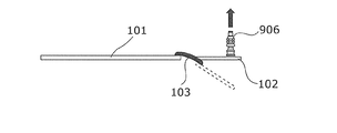
図2Aは、ドライバ基板付き表示パネルを移載するために真空吸着を用いて保持する方法を模式的に示す図である。図2Bは、図2Aを側面からみた図である。図1と同様の要素には同一の符号を付しており、詳細な説明は省略する。
図2Aおよび図2Bに示すように、表示パネル101を吸着パッド905で真空吸着して保持するとともにドライバ基板102を吸着パッド906で真空吸着して保持することで、ドライバ基板付き表示パネル100を移載することができる。
しかしながら、吸着パッド905は、ドライバ基板102に実装されている複数の部品(部品実装位置)を避けて真空吸着する必要がある。つまり、ドライバ基板102には吸着できる位置(吸着場所)に制約がある。また、ドライバ基板102の寸法および形状が変化する場合には部品実装位置も変更になるため、吸着場所も変更しなければならない。さらに、ドライバ基板102に実装される複数の部品や配線が高密度化すると吸着場所そのものがない場合も発生する。
[本発明の一実施の形態の移載装置および移載方法の説明]
以下、本開示における移載装置および移載方法について、説明する。
以下、本開示における移載装置および移載方法について、説明する。
[実施の形態1の移載装置の構成]
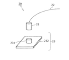
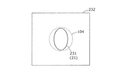
図3は、実施の形態1に係る移載装置の構成を模式的に示す図である。図4は、実施の形態1に係るマグネットの構成の別の一例を示す図である。図5Aは、実施の形態1に係る移載装置を上からみた場合の形状の一例を示す図である。図5Bは、実施の形態1に係る移載装置を上からみた場合の形状の別の一例を示す図である。
図3は、実施の形態1に係る移載装置の構成を模式的に示す図である。図4は、実施の形態1に係るマグネットの構成の別の一例を示す図である。図5Aは、実施の形態1に係る移載装置を上からみた場合の形状の一例を示す図である。図5Bは、実施の形態1に係る移載装置を上からみた場合の形状の別の一例を示す図である。
図3に示すように、移載装置20は、ドライバ基板102を移載するために用いる移載装置であって、紐状体22に連結されたマグネット21と、基板受け治具23とを備える。
基板受け治具23は、突出部231と、平板部232とを有する。
突出部231は、平板部232に形成され、ドライバ基板102が有する穴であって予め定められた大きさの穴である取付穴104を貫通するように挿入可能に形成されている。突出部231は、磁力により吸着される金属であり、例えば、鉄、コバルト、ニッケルや、これらを含む合金である。
平板部232は、ドライバ基板102の下面の少なくとも一部に当接することでドライバ基板102を支持する。平板部232は、軽量化を目的とする材質であれば良く、例えば、アルミニウムや銅鉄、アクリル樹脂などを挙げることができる。
マグネット21は、一端が紐状体22に連結され、所定の高さに吊り下げられる。マグネット21は、突出部231の先端部を磁力で吸着することで、基板受け治具23を所定の高さに保持する。例えば、マグネット21は、典型的には永久磁石で構成されるが、電磁石で構成されるとしてもよい。
なお、マグネット21は、一端が紐状体22と溶接等により直接連結されているとしてもよいが、図4に示すようにマグネット21に形成された連結部材211に紐状体22を貫通させて縛るなどして連結するとしてもよい。
また、突出部231およびマグネット21を上からみた場合の形状は、例えば図5Aに示すように、取付穴104よりも小さい楕円形である。これにより、突出部231は、取付穴104に挿入するのが容易となる。もちろん、突出部231およびマグネット21を上からみた場合の形状は、例えば図5Bに示すように、例えば直径8mm程度の円形など取付穴104よりも小さい円形であってもよい。取付穴104に支障なく滑らかに挿入でき、かつ、取付穴104を介してドライバ基板102の水平方向のずれを抑制できればその形状は任意である。
紐状体22は、例えば静電気が防止されたロープやケーブル、金属ワイヤ等で構成され、一定の長さを有する。紐状体22は、一端がマグネット21と連結され、多端が一定の高さで固定されることにより、マグネット21を所定の高さに吊り下げることができる。ここで、所定の高さとは、例えば表示パネル101が保持される高さである。
[実施の形態1の移載装置を用いた基板の移載方法]
ここで、図6、図7Aおよび図7Bを用いて、ドライバ基板付き表示パネル100を移載するために移載装置20を用いる場合について説明する。
ここで、図6、図7Aおよび図7Bを用いて、ドライバ基板付き表示パネル100を移載するために移載装置20を用いる場合について説明する。
図6は、本開示の移載方法を説明するためのフローチャートである。図7Aは、ドライバ基板付き表示パネルを移載するために実施の形態1の移載装置を用いて保持する方法を模式的に示す図である。図7Bは、図7Aを側面からみた図である。なお、図1、図2Aおよび図2Bと同様の要素には同一の符号を付しており、詳細な説明は省略する。
まず、基板受け治具23の突出部231を、ドライバ基板102の取付穴104を貫通するように、取付穴104に挿入させる(S101)。
次に、基板受け治具23の平板部232にドライバ基板102の下面の少なくとも一部に当接させることで、基板受け治具23にドライバ基板102を支持させる(S102)。
次に、複数のマグネット21のそれぞれに、基板受け治具23の突出部231の先端部を磁力により吸着させることで、例えば図7Bに示すように、基板受け治具23を所定の高さに保持する(S103)。
ここで、複数のマグネット21のそれぞれは、一端が紐状体22に連結されることで所定の高さに保持される。換言すると、紐状体22のそれぞれは、多端が一定の高さに固定され、一端がマグネット21の一端と連結されることで、マグネット21を所定の高さに保持することができる。
このように、ドライバ基板102の取付穴104に基板受け治具23を取り付け、基板受け治具23をマグネット21で保持することで、ドライバ基板付き表示パネル100のうちのドライバ基板102を保持することができる。
なお、表示パネル101は、例えば図7Aに示すように、移載装置20を用いずに、真空吸着等の別の方法で所定の高さに保持される。このようにして、移載装置20を用いて保持されたドライバ基板付き表示パネル100は、表示パネル101と略同一の高さで保持することができる。
[効果等]
本実施の形態によれば、例えば図7Aおよび図7Bに示すように、表示パネル101を吸着パッド905で真空吸着して保持するとともにドライバ基板102を移載装置20で磁力により吸着して保持することで、ドライバ基板付き表示パネル100を表示パネル101と略同一の高さで保持しながら移載することができる。
本実施の形態によれば、例えば図7Aおよび図7Bに示すように、表示パネル101を吸着パッド905で真空吸着して保持するとともにドライバ基板102を移載装置20で磁力により吸着して保持することで、ドライバ基板付き表示パネル100を表示パネル101と略同一の高さで保持しながら移載することができる。
なお、ドライバ基板付き表示パネル100を移載する際に、ドライバ基板102のたわみを防止するため、表示パネル101とドライバ基板102とを同時に保持するとよい。
また、マグネット21は移動自由であり、基板受け治具23(特に平板部232)はドライバ基板に合わせて容易に作成することができるので、ドライバ基板の寸法、形状に対して安価に対応できる。具体的には、ドライバ基板102の保持を本実施の形態の移載装置20を用いて行うことで、表示パネル101のサイズ変更に伴うドライバ基板102の部品配置変更があっても、移載装置20の数を増やすだけで対応できる。
さらに、マグネット21を用いる構成であることから、紐状体22と基板受け治具23との着脱が非常に容易となり作業性が大幅に向上するという効果も得られる。
このようにして、寸法および形状に依存しない基板保持に有効な移載装置およびそれを用いた移載方法を実現することができるだけでなく、表示パネル101のサイズやドライバ基板102の部品配置変更時などにおける移載設備に必要な改造費用の削減が可能となる。
(実施の形態2)
実施の形態1では、基板受け治具23の構成の一例を挙げて説明したが、それに限らない。本実施の形態では、基板受け治具23の構成の別の一例について説明する。
実施の形態1では、基板受け治具23の構成の一例を挙げて説明したが、それに限らない。本実施の形態では、基板受け治具23の構成の別の一例について説明する。
以下では、実施の形態1と同様の部分は説明を省略し、異なる点を中心に説明する。
[実施の形態2の移載装置の構成]
図8は、実施の形態2に係る基板受け治具の構成を模式的に示す図である。なお、図3と同様の要素には同一の符号を付しており、詳細な説明は省略する。
図8は、実施の形態2に係る基板受け治具の構成を模式的に示す図である。なお、図3と同様の要素には同一の符号を付しており、詳細な説明は省略する。
基板受け治具23Aは、複数の平板部232と、複数の突出部231と、連結部233とを有する。本実施の形態では、基板受け治具23Aは、図8に示すように2つの平板部232を有する。
突出部231は、複数の平板部232それぞれに形成され、取付穴104を貫通するように挿入可能に形成されている。本実施の形態では、突出部231は、図8に示すように、2つの平板部232それぞれに1つずつ形成されている。
平板部232は、ドライバ基板102の下面の少なくとも一部に当接することでドライバ基板102を支持する。
連結部233は、複数の平板部232を略平面に維持し、かつ、複数の平板部232の一端部同士を連結する。本実施の形態では、図8に示すように、連結部233は、2つの平板部232を略平面に維持し、かつ、2つの平板部232の一端同士を連結する。また、連結部233は、軽量化を目的とする材質であれば良く、例えば、アルミニウムや銅鉄、アクリル樹脂などを挙げることができる。
以上のように構成された基板受け治具23Aは、マグネット21により、2つの平板部232それぞれに形成された突出部231の先端部が磁力で吸着されることで、所定の高さに保持される。なお、マグネット21は、複数あり、紐状体22も複数ある。本実施の形態では、複数のマグネット21のそれぞれは、一端が紐状体22に連結され、所定の高さに吊り下げられる。
なお、本実施の形態では、複数の平板部232が2つの場合を一例として挙げたがそれに限らない。例えば図9に示すように複数の平板部232が3つで構成されるとしてもよい。
図9は、実施の形態2に係る基板受け治具の構成の別の一例を模式的に示す図である。なお、図8と同様の要素には同一の符号を付しており、詳細な説明は省略する。
図9に示す基板受け治具23Bは、3つ平板部232と、複数の突出部231と、連結部233とを有する。
連結部233Aは、図9に示すように、3つの平板部232を略平面に維持し、かつ、3つの平板部232の一端部同士を連結する。
したがって、基板受け治具23Bは、複数のマグネット21それぞれにより、3つの平板部232それぞれに形成された突出部231の先端部が磁力で吸着されることで、所定の高さに保持される。なお、上述したように、各マグネット21は、一端が紐状体22に連結され、所定の高さに吊り下げられる。
(実施の形態3)
実施の形態3では、実施の形態2で挙げた基板受け治具のさらに別の構成の一例について説明する。なお、以下では、実施の形態1および2と同様の部分は説明を省略し、異なる点を中心に説明する。
実施の形態3では、実施の形態2で挙げた基板受け治具のさらに別の構成の一例について説明する。なお、以下では、実施の形態1および2と同様の部分は説明を省略し、異なる点を中心に説明する。
[実施の形態3の移載装置の構成]
図10は、実施の形態3に係る基板受け治具の構成を模式的に示す図である。なお、図3および図8と同様の要素には同一の符号を付しており、詳細な説明は省略する。
図10は、実施の形態3に係る基板受け治具の構成を模式的に示す図である。なお、図3および図8と同様の要素には同一の符号を付しており、詳細な説明は省略する。
基板受け治具23Cは、複数の平板部232と、複数の突出部231と、連結部233とを有する。本実施の形態では、基板受け治具23Cは、図10に示すように、2つの平板部232と、平板部232それぞれに2つの突出部231(突出部231Aおよび231B)を有する。
突出部231Aおよび231Bは、図10に示すように、2つの平板部232それぞれに形成され、取付穴104を貫通するように挿入可能に形成されている。
突出部231Aは、2つの突出部のうちの第1突出部の一例であり、ドライバ基板102の取付穴104を貫通するように取付穴104に挿入される。突出部231Bは、2つの突出部のうちの第2突出部の一例であり、突出部231Aよりも平板部232の一端部側に形成されている。ここで、突出部231Aおよび231Bの一方の先端部がマグネット21の磁力で吸着されるのに対して、他方の先端部はマグネット21が吸着されない。
[実施の形態3の移載装置の使用例]
図11は、実施の形態3に係る基板受け治具の使用例を模式的に示す図である。なお、図10と同様の要素には同一の符号を付しており、詳細な説明は省略する。
図11は、実施の形態3に係る基板受け治具の使用例を模式的に示す図である。なお、図10と同様の要素には同一の符号を付しており、詳細な説明は省略する。
実施の形態3に係る基板受け治具23Cは、図11に示すように、突出部231Aおよび231Bの一方の先端部がマグネット21の磁力で吸着されるのに対して、他方の先端部はマグネット21が吸着されない。つまり、マグネット21のそれぞれは、突出部231Aより平板部232の一端部側に形成された突出部231Bの先端部と突出部231Aの先端部とを、1以上の平板部232ごとに交互に、磁力で吸着する。
それにより、マグネット21のそれぞれは、連結部233のしなりやねじれを防止しつつ、基板受け治具23Cを所定の高さに保持することができる。
[効果等]
本実施の形態によれば、ドライバ基板102の取付穴104に基板受け治具23を取り付け、基板受け治具23をマグネット21で保持することで、基板受け治具23Cを所定の高さに保持することができる。
本実施の形態によれば、ドライバ基板102の取付穴104に基板受け治具23を取り付け、基板受け治具23をマグネット21で保持することで、基板受け治具23Cを所定の高さに保持することができる。
さらに、本実施の形態によれば、ドライバ基板102の取付穴104に基板受け治具23Cを取り付け、基板受け治具23の2つの突出部231を平板部232ごとに交互にマグネット21で保持することで、基板受け治具23の連結部233のしなりやねじれを防止することができ、ドライバ基板102をより略平行に保持することができるという効果を奏する。
また、マグネット21は移動自由であり、基板受け治具23(特に平板部232)はドライバ基板に合わせて容易に作成することができるので、ドライバ基板の寸法、形状に対して安価に対応できる。さらに、マグネット21を用いる構成であることから、紐状体22と基板受け治具23との着脱が非常に容易となることから作業性が大幅に向上するという効果も得られる。
したがって、本実施の形態によれば、寸法および形状に依存しない基板保持に有効な移載装置およびそれを用いた移載方法を実現することができる。
なお、本実施の形態では、複数の平板部232が2つの場合を一例として挙げたがそれに限らない。例えば図12に示すように複数の平板部232が3つで構成されるとしてもよい。以下、この場合について説明する。
図12は、実施の形態3に係る基板受け治具の構成の別の一例を模式的に示す図である。なお、図11と同様の要素には同一の符号を付しており、詳細な説明は省略する。
図12に示す基板受け治具23Dは、3つ平板部232と、複数の突出部231と、連結部233とを有する。
本実施の形態では、基板受け治具23Dは、図12に示すように、3つの平板部232と、平板部232それぞれに2つの突出部231(突出部231Aおよび231B)を有する。
また、連結部233Bは、図12に示すように、3つの平板部232を略平面に維持し、かつ、3つの平板部232の一端部同士を連結する。
そして、基板受け治具23Dは、複数のマグネット21それぞれにより、3つの平板部232それぞれに形成された突出部231Aおよび突出部231Bの一方の先端部が磁力で吸着されることで、所定の高さに保持される。つまり、マグネット21のそれぞれは、突出部231Aより平板部232の一端部側に形成された突出部231Bの先端部と突出部231Aの先端部とを、複数の平板部232ごとに交互に、磁力で吸着する。
このようにして、マグネット21のそれぞれは、連結部233のしなりやねじれを防止しつつ、基板受け治具23Dを所定の高さに保持することができる。
(他の実施の形態)
以上のように、本開示における技術の例示として、実施の形態1~3を説明した。そのために、添付図面および詳細な説明を提供した。
以上のように、本開示における技術の例示として、実施の形態1~3を説明した。そのために、添付図面および詳細な説明を提供した。
したがって、添付図面および詳細な説明に記載された構成要素の中には、課題解決のために必須な構成要素だけでなく、上記技術を例示するために、課題解決のためには必須でない構成要素も含まれ得る。そのため、それらの必須ではない構成要素が添付図面や詳細な説明に記載されていることをもって、直ちに、それらの必須ではない構成要素が必須であるとの認定をするべきではない。
また、上述の実施の形態は、本開示における技術を例示するためのものであるから、請求の範囲またはその均等の範囲において種々の変更、置き換え、付加、省略などを行うことができる。つまり、本開示における技術は、これに限定されず、適宜、変更、置き換え、付加、省略などを行った実施の形態にも適用可能である。また、上記実施の形態1~3で説明した各構成要素を組み合わせて、新たな実施の形態とすることも可能である。
また、以下のような場合も本開示に含まれる。
例えば実施の形態1では、平板部の上からみたときの形状の一例として、四角形であるとして図示したが、それにかぎらず楕円でも円形でも、多角形でもよい。ドライバ基板を支持することができればその形状は四角形に限定されるものではない。
例えば実施の形態1~3では、基板を、表示パネルにフレキシブル配線で接続されているドライバ基板であるとして説明したがそれに限られない。表示パネルに搭載されたドライバ基板であってもよいし、ドライバ基板以外の基板であってもよい。規格や仕様等で予め定められた大きさの取付穴を流用できるものであれば、基板の種類は問わない。
また、実施の形態1~3では、ドライバ基板が表示パネルの周辺に取り付けられている場合を例に挙げて説明しているが、それに限らない。ドライバ基板が表示パネルの一辺にのみ接続されているとしてもよい。つまり、ドライバ基板が取り付けられる個数も限定されるものではない。
本開示は、寸法および形状に依存しない基板保持に有効な移載装置およびそれを用いた移載方法に適用可能である。具体的には、表示パネルに接続されたドライバ基板の保持するための移載装置およびそれを用いた移載設備などに、本開示は適用可能である。
20 移載装置
21 マグネット
22 紐状体
23、23A、23B、23C、23D 基板受け治具
100 ドライバ基板付き表示パネル
101 表示パネル
102 ドライバ基板
103 フレキシブル基板
104 取付穴
211 連結部材
231、231A、231B 突出部
232 平板部
233、233A、233B 連結部
905、906 吸着パッド
21 マグネット
22 紐状体
23、23A、23B、23C、23D 基板受け治具
100 ドライバ基板付き表示パネル
101 表示パネル
102 ドライバ基板
103 フレキシブル基板
104 取付穴
211 連結部材
231、231A、231B 突出部
232 平板部
233、233A、233B 連結部
905、906 吸着パッド
Claims (8)
- 基板を移載するために用いる移載装置であって、
一端が紐状体に連結され、所定の高さに吊り下げられるマグネットと、
前記基板の下面の少なくとも一部に当接することで前記基板を支持する平板部と、前記平板部に形成され、前記基板が有する穴であって予め定められた大きさの穴を貫通するように挿入可能な突出部とを有する基板受け治具と、を備え、
前記マグネットは、前記突出部の先端部を磁力で吸着することで、前記基板受け治具を所定の高さに保持する、
移載装置。 - 前記基板受け治具は、
複数の前記平板部と、
前記複数の平板部それぞれに形成された前記突出部と、
複数の前記平板部を略平面に維持し、かつ、複数の前記平板部の一端部同士を連結する連結部とを備え、
前記マグネットは、複数であり、
前記複数のマグネットのそれぞれは、前記複数の平板部それぞれに形成された前記突出部の先端部を磁力で吸着することで、前記基板受け治具を前記所定の高さに保持する、
請求項1に記載の移載装置。 - 前記複数の平板部は、2つの前記平板部からなる、
請求項2に記載の移載装置。 - 前記複数の平板部それぞれには、2つの前記突出部が形成されており、
前記2つの突出部のうちの第1突出部は、前記穴を貫通するように挿入され、
前記マグネットのそれぞれは、前記2つの突出部のうち前記第1突出部より前記一端部側に形成された第2突出部の先端部と前記第1突出部の先端部とを、1以上の前記平板部ごとに交互に、磁力で吸着することで、前記基板受け治具を前記所定の高さに保持する、
請求項2または3に記載の移載装置。 - 前記マグネットの数は、偶数である、
請求項2~4のいずれか1項に記載の移載装置。 - 前記マグネットは、電磁石である、
請求項2~5のいずれか1項に記載の移載装置。 - 前記基板は、表示パネルにフレキシブル配線で接続されるドライバ基板であり、
前記所定の高さは、前記表示パネルが保持される高さである、
請求項1~6のいずれか1項に記載の移載装置。 - 請求項1に記載の移載装置を用いて、前記基板を移載する方法であって、
前記突出部を、前記基板が有する前記穴を貫通するように挿入させ、かつ、前記平板部に前記基板の下面の少なくとも一部に当接させることで、前記基板受け治具に前記基板を支持させ、
複数の前記マグネットのそれぞれに、前記突出部の先端部を磁力により吸着させることで、前記基板受け治具を前記所定の高さに保持する、
移載方法。
Applications Claiming Priority (2)
| Application Number | Priority Date | Filing Date | Title |
|---|---|---|---|
| JP2013216723 | 2013-10-17 | ||
| JP2013-216723 | 2013-10-17 |
Publications (1)
| Publication Number | Publication Date |
|---|---|
| WO2015056368A1 true WO2015056368A1 (ja) | 2015-04-23 |
Family
ID=52827834
Family Applications (1)
| Application Number | Title | Priority Date | Filing Date |
|---|---|---|---|
| PCT/JP2014/002506 Ceased WO2015056368A1 (ja) | 2013-10-17 | 2014-05-13 | 移載装置および移載方法 |
Country Status (1)
| Country | Link |
|---|---|
| WO (1) | WO2015056368A1 (ja) |
Cited By (1)
| Publication number | Priority date | Publication date | Assignee | Title |
|---|---|---|---|---|
| CN114460069A (zh) * | 2020-11-10 | 2022-05-10 | 艾康生物技术(杭州)有限公司 | 具有试纸定位结构的检测装置及检测试纸 |
Citations (2)
| Publication number | Priority date | Publication date | Assignee | Title |
|---|---|---|---|---|
| JP2007152454A (ja) * | 2005-12-01 | 2007-06-21 | Nippon Mektron Ltd | 板状ワークの吸着搬送装置および搬送方法 |
| JP2012068301A (ja) * | 2010-09-21 | 2012-04-05 | Sharp Corp | 表示装置およびテレビ受信装置 |
-
2014
- 2014-05-13 WO PCT/JP2014/002506 patent/WO2015056368A1/ja not_active Ceased
Patent Citations (2)
| Publication number | Priority date | Publication date | Assignee | Title |
|---|---|---|---|---|
| JP2007152454A (ja) * | 2005-12-01 | 2007-06-21 | Nippon Mektron Ltd | 板状ワークの吸着搬送装置および搬送方法 |
| JP2012068301A (ja) * | 2010-09-21 | 2012-04-05 | Sharp Corp | 表示装置およびテレビ受信装置 |
Cited By (1)
| Publication number | Priority date | Publication date | Assignee | Title |
|---|---|---|---|---|
| CN114460069A (zh) * | 2020-11-10 | 2022-05-10 | 艾康生物技术(杭州)有限公司 | 具有试纸定位结构的检测装置及检测试纸 |
Similar Documents
| Publication | Publication Date | Title |
|---|---|---|
| CN200944704Y (zh) | 一种柔性电路基板(fpc)装联用的夹具 | |
| JP2011060829A (ja) | フレキシブルプリント基板の搬送用キャリア及びそれを用いたフレキシブルプリント基板の印刷装置 | |
| CN111326074A (zh) | 显示装置、平铺显示装置以及制造平铺显示装置的方法 | |
| WO2008057450A3 (en) | Magnetic component connector, circuit boards for use therewith, and kits for building and designing circuits | |
| JP2015503111A (ja) | 再使用可能な、電子回路の組み立ておよび試験システム、およびその使用 | |
| US9401239B2 (en) | Electrical component for attachment to paper and other substrates and magnetic attachment mechanism | |
| CN102044332B (zh) | 变压器以及变压器组件 | |
| KR20130047337A (ko) | 카메라 모듈 | |
| WO2015056368A1 (ja) | 移載装置および移載方法 | |
| US20100084164A1 (en) | Electronic component mounting method | |
| JP6058143B2 (ja) | Oled照明モジュール | |
| KR101920318B1 (ko) | 카메라 모듈 | |
| TWI829172B (zh) | 巨量轉移系統及巨量轉移方法 | |
| JP2009087676A (ja) | 電気器具取付け装置 | |
| CN215121363U (zh) | 适用于双面有元器件的pcba板载板治具 | |
| WO2016026267A1 (zh) | 载物台和热压设备 | |
| KR101538099B1 (ko) | 인쇄회로기판 이송용 캐리어 지그 | |
| JP2008186993A (ja) | プリント基板支持装置 | |
| EP2933551A1 (en) | A lighting device and corresponding method | |
| US7482688B2 (en) | Attaching heat sinks to integrated circuit packages | |
| CN109041449B (zh) | 回流焊载具 | |
| CN111031689B (zh) | 一种夹具、柔性线路板、显示面板及其弯折方法 | |
| JP2015076137A (ja) | コネクタ | |
| JP4244196B2 (ja) | 導電性ボールの搭載装置 | |
| CN214027577U (zh) | 带有磁力片的覆铜板 |
Legal Events
| Date | Code | Title | Description |
|---|---|---|---|
| 121 | Ep: the epo has been informed by wipo that ep was designated in this application |
Ref document number: 14854305 Country of ref document: EP Kind code of ref document: A1 |
|
| NENP | Non-entry into the national phase |
Ref country code: DE |
|
| NENP | Non-entry into the national phase |
Ref country code: JP |
|
| 122 | Ep: pct application non-entry in european phase |
Ref document number: 14854305 Country of ref document: EP Kind code of ref document: A1 |