WO2015034095A1 - パターン形成方法及びこの方法を用いたタッチパネルの製造方法 - Google Patents
パターン形成方法及びこの方法を用いたタッチパネルの製造方法 Download PDFInfo
- Publication number
- WO2015034095A1 WO2015034095A1 PCT/JP2014/073739 JP2014073739W WO2015034095A1 WO 2015034095 A1 WO2015034095 A1 WO 2015034095A1 JP 2014073739 W JP2014073739 W JP 2014073739W WO 2015034095 A1 WO2015034095 A1 WO 2015034095A1
- Authority
- WO
- WIPO (PCT)
- Prior art keywords
- pattern
- sputtering
- film
- mask
- mask sheet
- Prior art date
- Legal status (The legal status is an assumption and is not a legal conclusion. Google has not performed a legal analysis and makes no representation as to the accuracy of the status listed.)
- Ceased
Links
Images












Classifications
-
- C—CHEMISTRY; METALLURGY
- C23—COATING METALLIC MATERIAL; COATING MATERIAL WITH METALLIC MATERIAL; CHEMICAL SURFACE TREATMENT; DIFFUSION TREATMENT OF METALLIC MATERIAL; COATING BY VACUUM EVAPORATION, BY SPUTTERING, BY ION IMPLANTATION OR BY CHEMICAL VAPOUR DEPOSITION, IN GENERAL; INHIBITING CORROSION OF METALLIC MATERIAL OR INCRUSTATION IN GENERAL
- C23C—COATING METALLIC MATERIAL; COATING MATERIAL WITH METALLIC MATERIAL; SURFACE TREATMENT OF METALLIC MATERIAL BY DIFFUSION INTO THE SURFACE, BY CHEMICAL CONVERSION OR SUBSTITUTION; COATING BY VACUUM EVAPORATION, BY SPUTTERING, BY ION IMPLANTATION OR BY CHEMICAL VAPOUR DEPOSITION, IN GENERAL
- C23C14/00—Coating by vacuum evaporation, by sputtering or by ion implantation of the coating forming material
- C23C14/06—Coating by vacuum evaporation, by sputtering or by ion implantation of the coating forming material characterised by the coating material
- C23C14/14—Metallic material, boron or silicon
- C23C14/18—Metallic material, boron or silicon on other inorganic substrates
- C23C14/185—Metallic material, boron or silicon on other inorganic substrates by cathodic sputtering
-
- C—CHEMISTRY; METALLURGY
- C23—COATING METALLIC MATERIAL; COATING MATERIAL WITH METALLIC MATERIAL; CHEMICAL SURFACE TREATMENT; DIFFUSION TREATMENT OF METALLIC MATERIAL; COATING BY VACUUM EVAPORATION, BY SPUTTERING, BY ION IMPLANTATION OR BY CHEMICAL VAPOUR DEPOSITION, IN GENERAL; INHIBITING CORROSION OF METALLIC MATERIAL OR INCRUSTATION IN GENERAL
- C23C—COATING METALLIC MATERIAL; COATING MATERIAL WITH METALLIC MATERIAL; SURFACE TREATMENT OF METALLIC MATERIAL BY DIFFUSION INTO THE SURFACE, BY CHEMICAL CONVERSION OR SUBSTITUTION; COATING BY VACUUM EVAPORATION, BY SPUTTERING, BY ION IMPLANTATION OR BY CHEMICAL VAPOUR DEPOSITION, IN GENERAL
- C23C14/00—Coating by vacuum evaporation, by sputtering or by ion implantation of the coating forming material
- C23C14/04—Coating on selected surface areas, e.g. using masks
- C23C14/042—Coating on selected surface areas, e.g. using masks using masks
-
- C—CHEMISTRY; METALLURGY
- C23—COATING METALLIC MATERIAL; COATING MATERIAL WITH METALLIC MATERIAL; CHEMICAL SURFACE TREATMENT; DIFFUSION TREATMENT OF METALLIC MATERIAL; COATING BY VACUUM EVAPORATION, BY SPUTTERING, BY ION IMPLANTATION OR BY CHEMICAL VAPOUR DEPOSITION, IN GENERAL; INHIBITING CORROSION OF METALLIC MATERIAL OR INCRUSTATION IN GENERAL
- C23C—COATING METALLIC MATERIAL; COATING MATERIAL WITH METALLIC MATERIAL; SURFACE TREATMENT OF METALLIC MATERIAL BY DIFFUSION INTO THE SURFACE, BY CHEMICAL CONVERSION OR SUBSTITUTION; COATING BY VACUUM EVAPORATION, BY SPUTTERING, BY ION IMPLANTATION OR BY CHEMICAL VAPOUR DEPOSITION, IN GENERAL
- C23C14/00—Coating by vacuum evaporation, by sputtering or by ion implantation of the coating forming material
- C23C14/06—Coating by vacuum evaporation, by sputtering or by ion implantation of the coating forming material characterised by the coating material
- C23C14/08—Oxides
- C23C14/086—Oxides of zinc, germanium, cadmium, indium, tin, thallium or bismuth
-
- C—CHEMISTRY; METALLURGY
- C23—COATING METALLIC MATERIAL; COATING MATERIAL WITH METALLIC MATERIAL; CHEMICAL SURFACE TREATMENT; DIFFUSION TREATMENT OF METALLIC MATERIAL; COATING BY VACUUM EVAPORATION, BY SPUTTERING, BY ION IMPLANTATION OR BY CHEMICAL VAPOUR DEPOSITION, IN GENERAL; INHIBITING CORROSION OF METALLIC MATERIAL OR INCRUSTATION IN GENERAL
- C23C—COATING METALLIC MATERIAL; COATING MATERIAL WITH METALLIC MATERIAL; SURFACE TREATMENT OF METALLIC MATERIAL BY DIFFUSION INTO THE SURFACE, BY CHEMICAL CONVERSION OR SUBSTITUTION; COATING BY VACUUM EVAPORATION, BY SPUTTERING, BY ION IMPLANTATION OR BY CHEMICAL VAPOUR DEPOSITION, IN GENERAL
- C23C14/00—Coating by vacuum evaporation, by sputtering or by ion implantation of the coating forming material
- C23C14/22—Coating by vacuum evaporation, by sputtering or by ion implantation of the coating forming material characterised by the process of coating
- C23C14/34—Sputtering
Definitions
- the present invention relates to a pattern forming method and a touch panel manufacturing method, and more particularly, by combining a pattern formed by sputtering using a plurality of sputtering masks to form a single pattern, thereby performing an exposure process and a developing process.
- the present invention relates to a pattern forming method and a touch panel manufacturing method which simplify the manufacturing by eliminating the need and reduce the cost of equipment by eliminating the exposure apparatus and the developing apparatus.
- a conventional capacitive touch panel is composed of a metal film, an insulating film, a transparent electrode film, etc., and detects the capacitance of the fingertip to detect where in the panel is touched by X and Y coordinates. .
- the metal film, the insulating film, and the transparent electrode film are patterned as follows. After forming each film and applying a photoresist on the film, exposure and development are performed to form a photoresist pattern. Each film is etched using the patterned photoresist as a mask (see, for example, Patent Document 1).
- the conventional pattern forming method requires a photoresist coating process, an exposure process, a developing process, an etching process, and a photoresist peeling process on a film to be patterned.
- the touch panel manufacturing method using the conventional pattern forming method needs to repeat the complicated and many photo processes as described above for each of the metal film, the insulating film, and the transparent electrode film.
- the photo line uses an exposure apparatus and a developing apparatus, there is a problem that capital investment and running cost are increased.
- the problem to be solved by the present invention that addresses such problems is to form a single pattern by synthesizing a pattern formed by sputtering using a plurality of sputtering masks, thereby exposing the exposure process.
- the present invention provides a pattern forming method and manufacturing method of a touch panel using this method, in which the manufacturing process is simplified by eliminating the development process, and the cost of equipment is reduced by eliminating the exposure apparatus and the development apparatus.
- a pattern forming method performs sputtering film formation a plurality of times using a plurality of sputtering masks having an opening pattern obtained by dividing a pattern to be formed on an object surface, A single pattern is formed by synthesizing the respective patterns formed by the sputtering mask.
- the opening pattern may be divided in the longitudinal direction of the pattern.
- the single pattern may be at least a part of a pattern formed on the object surface.
- each of the plurality of sputtering masks may include a mask sheet having the opening pattern, and a frame that surrounds the mask sheet and on which the mask sheet is stretched.
- the mask sheet includes a resin mask sheet in which the opening pattern is formed in a resin film, a metal film in which a plurality of slit-shaped through holes are arranged in parallel, and a laminate on one surface of the metal film, Or a composite mask sheet having at least one resin film on which the opening pattern is formed, and a metal mask sheet on which a metal film is formed with the opening pattern.
- a touch panel manufacturing method is a touch panel manufacturing method including a metal film, an insulating film, and a transparent electrode film, and the metal film pattern is formed on a target surface.
- a plurality of first sputtering masks having an opening pattern obtained by dividing the wiring pattern to be sputtered, a plurality of sputtering films are formed, and the patterns formed by the plurality of first sputtering masks are combined to form a single wiring.
- a pattern is formed, and the pattern formation of the insulating film is performed by printing a photoresist pattern on the insulating film using a printing mask, and performing wet etching of the insulating film using the photoresist pattern as a mask.
- the transparent electrode film is patterned using a second sputtering mask having an opening pattern corresponding to the pattern to be formed. The over emissions reduction has been the transparent electrode film is to sputter deposition.
- the opening pattern of the first sputtering mask may be divided into a plurality of wirings in the longitudinal direction.
- each of the first and second sputtering masks and the printing mask may include a mask sheet having the opening pattern and a frame body that surrounds the mask sheet and is stretched. Good.
- the mask sheet is laminated on one surface of a resin mask sheet in which the opening pattern is formed in a resin film, a metal film in which a plurality of slit-shaped through holes are arranged in parallel, and the through hole
- a composite mask sheet having a resin film having at least one opening pattern formed therein and a metal mask sheet having the opening pattern formed in a metal film may be included.
- the pattern forming method of the present invention by using a plurality of sputtering masks having an opening pattern obtained by dividing a pattern to be formed on an object surface, a single composite pattern is formed by sputtering a plurality of times.
- the manufacturing process can be simplified by eliminating the exposure process and the development process, and the cost of the equipment can be reduced by eliminating the exposure apparatus and the development apparatus.
- the metal film, the insulating film, and the transparent electrode film can be patterned without using a photo process. Accordingly, the manufacturing process can be simplified by eliminating the exposure process and the development process, and the cost of the equipment can be reduced by eliminating the exposure apparatus and the development apparatus.
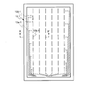
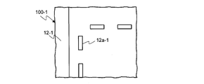
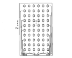
- FIG. 5 is a plan view of a first mask for sputtering, illustrating a first step in a method for manufacturing a touch panel according to the present invention.
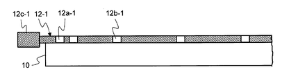
- FIG. 2B is an enlarged cross-sectional view taken along line X-X ′ of FIG. 2A.
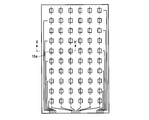
- FIG. 7 is a plan view of a second mask for sputtering, illustrating a second step in the method for manufacturing a touch panel according to the present invention.
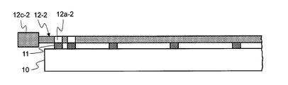
- FIG. 3B is an enlarged cross-sectional view taken along line X-X ′ of FIG. 3A. It is a top view of the wiring pattern formed at the 1st and 2nd process.
- FIG. 5 is a plan view of a first mask for sputtering, illustrating a first step in a method for manufacturing a touch panel according to the present invention.
- FIG. 2B is an enlarged cross-sectional view taken along line X-X ′ of FIG. 2A.
- FIG. 3B is an enlarged cross-sectional
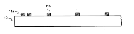
- FIG. 4B is an enlarged sectional view taken along line X-X ′ of FIG. 4A. It is an enlarged plan view of the opening pattern of FIG. 2A. It is an enlarged plan view of the opening pattern of FIG. 3A.
- FIG. 4B is an enlarged plan view of the combined wiring pattern of FIG. 4A. It is the top view which showed the 3rd process in the manufacturing method of the touchscreen by this invention, and formed the insulating film on the wiring pattern.
- FIG. 6B is an enlarged sectional view taken along line X-X ′ of FIG. 6A. It is the top view of the mask for printing in the 4th process in the manufacturing method of the touchscreen by this invention, and applying the photoresist.
- FIG. 7B is an enlarged sectional view taken along line X-X ′ of FIG. 7A. It is the top view of the resist pattern which shows the 5th process in the manufacturing method of the touchscreen by this invention.
- FIG. 8B is an enlarged sectional view taken along line X-X ′ of FIG. 8A.
- the 6th process in the manufacturing method of the touch panel by the present invention is shown, and is a top view of a resist pattern and a wiring pattern.
- FIG. 9B is an enlarged sectional view taken along line X-X ′ of FIG. 9A.
- the 7th process in the manufacturing method of the touch panel by the present invention is shown, and is a top view of a wiring pattern and an insulating film pattern.
- FIG. 10B is an enlarged sectional view taken along line X-X ′ of FIG. 10A. It is the top view of the mask for sputtering which shows the 8th process in the manufacturing method of the touchscreen by this invention.
- FIG. 11B is an enlarged sectional view taken along line X-X ′ of FIG. 11A.
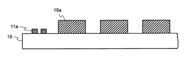
- FIG. 24 is a plan view of a Y-ITO film, illustrating a ninth step in the method for manufacturing a touch panel according to the present invention.
- FIG. 12B is an enlarged sectional view taken along line X-X ′ of FIG. 12A. It is the top view of the mask for sputtering which shows the 10th process in the manufacturing method of the touchscreen by this invention.
- FIG. 13B is an enlarged sectional view taken along line X-X ′ of FIG. 13A.
- FIG. 11 is a plan view of an X-ITO film, illustrating an eleventh step in the touch panel manufacturing method according to the present invention.
- FIG. 14B is an enlarged sectional view taken along line X-X ′ of FIG. 14A.
- FIG. 1 is a process diagram showing an embodiment of a touch panel manufacturing method according to the present invention.
- the touch panel manufacturing method includes a metal film pattern forming step (steps S1 to S5), an insulating film pattern forming step (steps S6 to S11), an ITO (Indium Tin Oxide) film (Y direction). ) Pattern formation step (steps S12 and S13) and ITO film (X direction) pattern formation step (steps S14 and S15).
- the metal film pattern forming process is performed by sputtering a plurality of times using a plurality of sputtering masks having an opening pattern obtained by dividing the pattern to be formed on the surface of the object, and by synthesizing the formed patterns into a single pattern. A pattern is formed.
- a photoresist pattern is formed by printing using a printing mask, and the metal film or the insulating film is wet etched using the photoresist pattern as a mask to form the pattern. It is.
- the pattern formation process of the ITO film (Y direction) and the ITO film (X direction) is patterned by performing sputtering film formation using a sputtering mask having an opening pattern corresponding to the pattern to be formed. An ITO film is formed.
- a first mask for sputtering 12-1 having an opening pattern 12a-1 obtained by dividing a pattern to be formed on the glass substrate 10 is positioned and installed (step S2). .
- the opening pattern 12a-1 is obtained by dividing the opening pattern of the adjacent long linear wiring pattern in the peripheral frame region in the longitudinal direction.
- the opening pattern 12b-1 at the center is relatively short and spaced apart, so that pattern deformation or displacement is unlikely to occur, so that the film is formed once without being divided.
- the first mask 12-1 for sputtering, sputtering film formation of a metal, for example, MAM (Mo / Al / Mo) is performed, and a part 11 of the wiring pattern is formed on the glass substrate 10 (process) S3).
- a metal for example, MAM (Mo / Al / Mo)
- the second mask for sputtering 12-2 is positioned and installed on the MAM film 11 (step S4).
- the second mask for sputtering 12-2 another opening pattern 12a-2 obtained by dividing a pattern to be formed on the glass substrate 10 is formed.
- the wiring pattern in the frame area around the wiring pattern 11 is complemented, and the combined patterns 11a and 11b are formed (step S5). Thereafter, cleaning is performed, and the formed wiring patterns 11a and 11b are inspected.
- the first mask for sputtering 12-1 is obtained by stretching a resin mask sheet in which opening patterns 12a-1 and 12b-1 are formed on a resin film such as polyimide, for example, inside a rectangular metal frame 12c-1. It is.
- the second mask for sputtering 12-2 is formed by stretching a resin mask sheet in which an opening pattern 12a-2 is formed on a resin film of polyimide or the like, for example, inside a rectangular metal frame 12c-2. . These resin films are held in a tensioned state.
- Each of the opening patterns 12a-1 and 12a-2 is a pattern obtained by dividing the pattern formed on the glass substrate 10 in the longitudinal direction as described above.
- a composite mask in which a resin film is laminated on one surface of a metal film (magnetic metal member) in which a plurality of slit-shaped through holes are arranged in parallel, and at least one opening pattern is formed in the through hole of the metal film.
- the sheet can be stretched and used inside a rectangular metal frame.
- the magnetic metal member can be attracted and fixed by a magnetic force.
- a metal mask sheet in which an opening pattern is formed on a metal film can be stretched and used inside a rectangular metal frame.
- the opening pattern 12a-1 of the first mask for sputtering 12-1 is formed by dividing the wiring pattern to be formed in the longitudinal direction, and a part thereof. It corresponds to the pattern of.
- the opening pattern 12a-2 of the second mask for sputtering 12-2 corresponds to the remaining portion of the wiring pattern divided in the longitudinal direction. is doing.
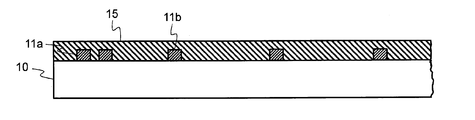
- an insulating film 15 for example, an organic insulating film such as SOG (Spin on Glass) is applied and formed on the entire surface (step S6).
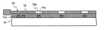
- a photoresist printing mask 16 is positioned and placed on the insulating film 15 (step S7).
- square opening patterns 16a are arranged in a matrix.
- a mask having the same structure as the sputtering mask can be used. Further, when they are spaced apart with a relatively simple pattern shape, a general screen printing mask can be used.
- a photoresist 17 is applied and printed on the printing mask 16 with the squeegee 13 (step S8).
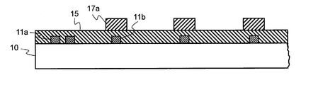
- a resist pattern 17a is formed on the insulating film 15 as shown in FIGS. 8A and 8B (step S9).
- step S10 wet etching of the insulating film 15 is performed using the resist pattern 17a as a mask. Then, when the resist pattern 17a is peeled off (step S11), the insulating film pattern 15a remains so as to cover a part of the wiring pattern 11b as shown in FIGS. 10A and 10B. Thereafter, cleaning is performed, and the formed insulating film pattern 15a is inspected.
- FIGS. 11A and 11B an opening pattern is formed on the glass substrate 10 on which the wiring patterns 11a and 11b and the insulating film pattern 15a covering a part of the wiring pattern 11b are formed as described above.
- the sputtering mask 18 having the 18a formed thereon is aligned and disposed, and an ITO film 19 is formed by sputtering in the opening pattern 18a (step S12). Since the ITO film 19 is formed in a pattern in the opening pattern 18a, as shown in FIGS. 12A and 12B, the ITO film 19 is electrically connected by the wiring pattern 11b, is continuous in the vertical direction, and has a position in the Y direction.
- the specified Y-ITO film 19a is formed (step S13). Thereafter, cleaning is performed, and the formed Y-ITO film 19a is inspected.
- the sputtering mask 20 having the opening pattern 20a is aligned on the glass substrate 10 on which the wiring pattern 11a, the insulating film pattern 15a and the Y-ITO film 19a are formed.
- the ITO film 21 is formed by sputtering on the insulating film in the opening pattern 20a (step S14). Since the ITO film 21 is formed in a pattern in the opening pattern 20a, as shown in FIGS. 14A and 14B, an X-ITO film 21a that is continuous in the horizontal direction and identifies the position in the X direction is formed. (Step S15).
- the insulating film pattern 15a is interposed between the patterned X-ITO film 21a and the Y-ITO film 19a so that the ITO films 21a and 19a are electrically separated.
- a mask having the same configuration as the Y-ITO film 19 a formed by sputtering (the shape of the opening pattern 20 a is different) can be used.
- a plurality of sputtering masks each having an opening pattern obtained by dividing a pattern to be formed on the surface of an object are sputtered multiple times, and the formed patterns are synthesized. A single pattern is formed. Accordingly, the manufacturing process can be simplified by eliminating the exposure process, the development process, and the etching process, and the cost of the equipment and the running cost can be reduced by eliminating the exposure apparatus and the development apparatus.
- the MAM film pattern formation uses a plurality of sputtering masks having an opening pattern obtained by dividing the wiring pattern to be formed on the object surface, so that a single composite pattern is formed by sputtering a plurality of times. There is little positional shift and deformation of the pattern of the sputtering mask, and film formation with high pattern accuracy can be performed.
- a photoresist pattern is formed by printing using a printing mask.
- a patterned metal layer and a transparent electrode film are formed using a sputtering mask. Therefore, since the photo process can be completely eliminated, the equipment cost and running cost can be greatly reduced.
- pattern formation methods of patterning by photoresist pattern printing and sputter deposition of patterned films metal films, insulating films, and transparent electrodes are suitable for each material and pattern shape.
- the patterning can be selected according to the method or the ease of forming the pattern.
- the sputter film formation can form a pattern without etching, by combining two pattern formation processes, not only the exposure process and the development process are omitted, but also the total number of manufacturing processes when forming the touch panel. Can be reduced.
- the method for manufacturing the capacitive touch panel has been described as an example.
- the present invention is not limited to the capacitive type, and can be applied to various other touch panel manufacturing methods.
- the touch panel manufacturing method has been described as an example to which the pattern forming method of the present invention is applied, it is needless to say that the present invention can be applied to the formation of various other patterns that perform wet etching or sputter film formation.
- an example of forming one composite pattern by forming a sputter film twice by using an opening pattern obtained by dividing the pattern to be formed has been shown.
- a composite pattern may be formed.
Landscapes
- Chemical & Material Sciences (AREA)
- Chemical Kinetics & Catalysis (AREA)
- Engineering & Computer Science (AREA)
- Materials Engineering (AREA)
- Mechanical Engineering (AREA)
- Metallurgy (AREA)
- Organic Chemistry (AREA)
- Inorganic Chemistry (AREA)
- Position Input By Displaying (AREA)
- Physical Vapour Deposition (AREA)
Abstract
Description
図1は、本発明によるタッチパネルの製造方法の実施形態を示す工程図である。このタッチパネルの製造方法は、金属膜(メタル)のパターン形成工程(工程S1~S5)、絶縁膜のパターン形成工程(工程S6~S11)、ITO(Indium Tin Oxide:酸化インジウムスズ)膜(Y方向)のパターン形成工程(工程S12,S13)、及びITO膜(X方向)のパターン形成工程(工程S14,S15)を含んでいる。
[金属膜のパターン形成工程]
まず、透明基板、例えばガラス基板10の表面を洗浄してスパッタ装置内に投入する(工程S1)。続いて、図2A及び図2Bに示すように、ガラス基板10上に形成するパターンを分割した開口パターン12a-1を有するスパッタ用第1マスク12-1を位置合わせして設置する(工程S2)。開口パターン12a-1は、周辺の額縁領域における、隣接し且つ直線状の長い配線パターンの開口パターンを長手方向に分割したものである。中央部の開口パターン12b-1は、比較的短く且つ離れて配置されており、パターンの変形やずれ等が生じにくいので分割せずに1回で成膜する。このように、スパッタ用第1マスク12-1を用いて、金属、例えばMAM(Mo/Al/Mo)のスパッタ成膜を行い、ガラス基板10上に配線パターンの一部11を形成する(工程S3)。
その後、洗浄を行い、形成した配線パターン11a,11bの検査を行う。
あるいは、スリット状の複数の貫通孔が並列配置された金属膜(磁性金属部材)の一面に、樹脂フィルムが積層され、金属膜の貫通孔内に少なくとも1つの開口パターンが形成された複合型マスクシートを、方形状のメタルフレームの内側に張設して用いることもできる。この複合マスクを用いると、磁性金属部材を磁力で吸着して固定できる。
さらに、金属膜に開口パターンを形成したメタルマスクシートを、方形状のメタルフレームの内側に張設して用いることもできる。
次に、図6A及び図6Bに示すように、全面に絶縁膜15、例えばSOG(Spin on Glass)等の有機絶縁膜を塗布形成する(工程S6)。その後、図7A及び図7Bに示すように、絶縁膜15上にフォトレジストの印刷用マスク16を位置合わせして設置する(工程S7)。この印刷用マスク16には、正方形の開口パターン16aがマトリックス状に配置されている。印刷用マスク16は、スパッタ用マスクと同様な構成のマスクを用いることができる。また、比較的単純なパターン形状で離隔して配置されている場合には、一般的なスクリーン印刷用のマスクを使用することもできる。そして、印刷用マスク16上にスキージ13でフォトレジスト17を塗布して印刷する(工程S8)。印刷用マスク16を除去すると、図8A及び図8Bに示すように、絶縁膜15上にレジストパターン17aが形成される(工程S9)。
その後、洗浄を行い、形成した絶縁膜パターン15aの検査を行う。
次に、図11A及び図11Bに示すように、前述したようにして、配線パターン11a,11bと、この配線パターン11bの一部を覆う絶縁膜パターン15aを形成したガラス基板10上に、開口パターン18aを形成したスパッタ用マスク18を位置合わせして配置し、開口パターン18a内にITO膜19をスパッタ成膜する(工程S12)。ITO膜19は、開口パターン18a内にパターン化されて形成されるので、図12A及び図12Bに示すように、配線パターン11bによって電気的に接続され、縦方向に連続し、Y方向の位置を特定するY-ITO膜19aが形成される(工程S13)。
その後、洗浄を行い、形成したY-ITO膜19aの検査を行う。
次に、図13A及び図13Bに示すように、配線パターン11a、絶縁膜パターン15a及びY-ITO膜19aを形成したガラス基板10上に、開口パターン20aを形成したスパッタ用マスク20を位置合わせして配置し、開口パターン20a内の絶縁膜上にITO膜21をスパッタ成膜する(工程S14)。ITO膜21は、開口パターン20a内にパターン化されて形成されるので、図14A及び図14Bに示すように、横方向に連続し、X方向の位置を特定するX-ITO膜21aが形成される(工程S15)。これらパターン化されたX-ITO膜21aとY-ITO膜19aとが交差する部分には、絶縁膜パターン15aが介在されて、両ITO膜21a,19aが電気的に分離される。
そして、ガラス基板10上の全面に絶縁膜を形成し、この絶縁膜上にカバーガラス等を設置する。
ここで、スパッタ用マスク20は、Y-ITO膜19aをスパッタ成膜する場合と同様な構成(開口パターン20aの形状が異なる)のマスクを用いることができる。
11…MAM膜(金属膜)
12-1,12-2…スパッタ用マスク
16…印刷用マスク
17…フォトレジスト
17a…レジストパターン
15…絶縁膜
15a…絶縁膜パターン
18,20…スパッタ用マスク
19,21…ITO膜(透明電極膜)
Claims (10)
- 対象物面上に形成するパターンを分割した開口パターンを有する複数のスパッタ用マスクを用いて、複数回スパッタ成膜し、前記複数のスパッタ用マスクでそれぞれ成膜したパターンを合成して単一のパターンを形成する、ことを特徴とするパターン形成方法。
- 前記開口パターンは、パターンの長手方向に分割されたものである、請求項1に記載のパターン形成方法。
- 前記単一のパターンは、対象物面上に形成するパターンの少なくとも一部である、請求項1に記載のパターン形成方法。
- 前記単一のパターンは、対象物面上に形成するパターンの少なくとも一部である、請求項2に記載のパターン形成方法。
- 前記複数のスパッタ用マスクはそれぞれ、前記開口パターンを有するマスクシートと、該マスクシートの周囲を囲み、該マスクシートが張設される枠体とを備える、請求項1乃至4いずれか1つの項に記載のパターン形成方法。
- 前記マスクシートは、樹脂フィルムに前記開口パターンが形成された樹脂マスクシート、スリット状の複数の貫通孔が並列配置された金属膜と、該金属膜の一面に積層され、前記貫通孔内に少なくとも1つの前記開口パターンが形成された樹脂フィルムとを有する複合型マスクシート、及び金属膜に前記開口パターンが形成されたメタルマスクシートのいずれかを含む、請求項5に記載のパターン形成方法。
- 金属膜、絶縁膜及び透明電極膜を含むタッチパネルの製造方法であって、
前記金属膜のパターン形成は、対象物面上に形成する配線パターンを分割した開口パターンを有する複数の第1スパッタ用マスクを用いて、複数回スパッタ成膜し、前記複数の第1スパッタ用マスクでそれぞれ成膜したパターンを合成して単一の配線パターンを形成し、
前記絶縁膜のパターン形成は、前記絶縁膜上に、印刷用マスクを用いてフォトレジストのパターンを印刷し、前記フォトレジストのパターンをマスクに前記絶縁膜のウェットエッチングを行ってパターニングし、
前記透明電極膜の形成は、形成すべきパターンに対応する開口パターンを有する第2スパッタ用マスクを用いてパターン化された透明電極膜をスパッタ成膜する、
ことを特徴とするタッチパネルの製造方法。 - 前記第1スパッタ用マスクの開口パターンは、配線の長手方向が複数に分割されたものである、請求項7に記載のタッチパネルの製造方法。
- 前記第1及び第2スパッタ用マスク、及び印刷用マスクはそれぞれ、前記開口パターンを有するマスクシートと、該マスクシートの周囲を囲み該マスクシートが張設される枠体とを備える、請求項7または8に記載のタッチパネルの製造方法。
- 前記マスクシートは、樹脂フィルムに前記開口パターンが形成された樹脂マスクシート、スリット状の複数の貫通孔が並列配置された金属膜と、該金属膜の一面に積層され、前記貫通孔内に少なくとも1つの前記開口パターンが形成された樹脂フィルムとを有する複合型マスクシート、及び金属膜に前記開口パターンが形成されたメタルマスクシートのいずれかを含む、請求項9に記載のタッチパネルの製造方法。
Priority Applications (2)
| Application Number | Priority Date | Filing Date | Title |
|---|---|---|---|
| KR1020167002005A KR20160053908A (ko) | 2013-09-09 | 2014-09-09 | 패턴 형성 방법 및 이 방법을 사용한 터치 패널의 제조 방법 |
| CN201480049456.5A CN105531393A (zh) | 2013-09-09 | 2014-09-09 | 图案形成方法以及使用该方法的触摸面板的制造方法 |
Applications Claiming Priority (2)
| Application Number | Priority Date | Filing Date | Title |
|---|---|---|---|
| JP2013-186256 | 2013-09-09 | ||
| JP2013186256A JP2015052156A (ja) | 2013-09-09 | 2013-09-09 | パターン形成方法及びこの方法を用いたタッチパネルの製造方法 |
Publications (1)
| Publication Number | Publication Date |
|---|---|
| WO2015034095A1 true WO2015034095A1 (ja) | 2015-03-12 |
Family
ID=52628552
Family Applications (1)
| Application Number | Title | Priority Date | Filing Date |
|---|---|---|---|
| PCT/JP2014/073739 Ceased WO2015034095A1 (ja) | 2013-09-09 | 2014-09-09 | パターン形成方法及びこの方法を用いたタッチパネルの製造方法 |
Country Status (5)
| Country | Link |
|---|---|
| JP (1) | JP2015052156A (ja) |
| KR (1) | KR20160053908A (ja) |
| CN (1) | CN105531393A (ja) |
| TW (1) | TW201519048A (ja) |
| WO (1) | WO2015034095A1 (ja) |
Families Citing this family (2)
| Publication number | Priority date | Publication date | Assignee | Title |
|---|---|---|---|---|
| KR101748826B1 (ko) * | 2015-07-16 | 2017-07-04 | 이민수 | 터치패널 및 그 터치패널 생성방법 |
| CN109445632A (zh) * | 2018-10-24 | 2019-03-08 | 信利光电股份有限公司 | 一种金属网格触摸屏制造方法 |
Citations (4)
| Publication number | Priority date | Publication date | Assignee | Title |
|---|---|---|---|---|
| JP2006077276A (ja) * | 2004-09-08 | 2006-03-23 | Seiko Epson Corp | マスク、マスクの製造方法、薄膜パターンの形成方法、電気光学装置の製造方法 |
| JP2006147557A (ja) * | 2004-11-18 | 2006-06-08 | Samsung Sdi Co Ltd | マスク組立体及びそれを用いたマスクフレーム組立体 |
| JP2012022941A (ja) * | 2010-07-15 | 2012-02-02 | Sk Link:Kk | マスクセット |
| JP2012111985A (ja) * | 2010-11-22 | 2012-06-14 | Toppan Printing Co Ltd | 蒸着マスクおよびそれを用いた薄膜パターン形成方法 |
-
2013
- 2013-09-09 JP JP2013186256A patent/JP2015052156A/ja active Pending
-
2014
- 2014-09-09 TW TW103130985A patent/TW201519048A/zh unknown
- 2014-09-09 WO PCT/JP2014/073739 patent/WO2015034095A1/ja not_active Ceased
- 2014-09-09 CN CN201480049456.5A patent/CN105531393A/zh active Pending
- 2014-09-09 KR KR1020167002005A patent/KR20160053908A/ko not_active Withdrawn
Patent Citations (4)
| Publication number | Priority date | Publication date | Assignee | Title |
|---|---|---|---|---|
| JP2006077276A (ja) * | 2004-09-08 | 2006-03-23 | Seiko Epson Corp | マスク、マスクの製造方法、薄膜パターンの形成方法、電気光学装置の製造方法 |
| JP2006147557A (ja) * | 2004-11-18 | 2006-06-08 | Samsung Sdi Co Ltd | マスク組立体及びそれを用いたマスクフレーム組立体 |
| JP2012022941A (ja) * | 2010-07-15 | 2012-02-02 | Sk Link:Kk | マスクセット |
| JP2012111985A (ja) * | 2010-11-22 | 2012-06-14 | Toppan Printing Co Ltd | 蒸着マスクおよびそれを用いた薄膜パターン形成方法 |
Also Published As
| Publication number | Publication date |
|---|---|
| CN105531393A (zh) | 2016-04-27 |
| KR20160053908A (ko) | 2016-05-13 |
| JP2015052156A (ja) | 2015-03-19 |
| TW201519048A (zh) | 2015-05-16 |
Similar Documents
| Publication | Publication Date | Title |
|---|---|---|
| US9229555B2 (en) | Touch screen panel and method of manufacturing the same | |
| KR100909265B1 (ko) | 정전용량 방식의 터치스크린 패널의 제조방법 | |
| CN107765917B (zh) | 一种触控面板的制备方法、触控面板和触控装置 | |
| TWI543035B (zh) | 觸控螢幕面板及其製造方法 | |
| US9011703B2 (en) | Method for manufacturing touch screen panel | |
| CN106775039B (zh) | 一种内嵌式触摸屏、其制作方法及显示装置 | |
| CN104407742A (zh) | 触控基板及其制备方法、显示装置 | |
| US9300288B2 (en) | Touch sensor panel and method for manufacturing the same | |
| CN104699308B (zh) | 一种触控面板的制作方法、触控面板及触控显示装置 | |
| KR20100095989A (ko) | 정전용량 방식의 터치스크린 패널의 제조방법 | |
| CN204242148U (zh) | 触控基板、显示装置 | |
| KR20140070106A (ko) | 플렉서블 터치스크린패널 및 그 제조방법 | |
| US20170060303A1 (en) | Method for manufacturing touch panel, touch panel and touch display device | |
| JP2013003915A (ja) | 投影型静電容量式タッチパネルセンサー及びその製造方法、投影型静電容量式タッチパネルセンサーを備えた表示装置 | |
| CN103487971A (zh) | 彩膜基板、触控显示装置及彩膜基板的制作方法 | |
| CN105518594A (zh) | 触摸面板的制造方法 | |
| TWI460771B (zh) | 觸控面板及其形成方法與顯示系統 | |
| JP2014016935A (ja) | フィルム状静電容量型タッチパネルの製造方法 | |
| DE202011052063U1 (de) | Elektrodenverbindung | |
| CN111625143B (zh) | 触控基板及其制作方法 | |
| JP2015052156A (ja) | パターン形成方法及びこの方法を用いたタッチパネルの製造方法 | |
| CN106783873A (zh) | 阵列基板及其制造方法、显示面板 | |
| US20140218638A1 (en) | Touch screen panel and method of manufacturing the same | |
| KR20150008703A (ko) | 정전용량 방식의 터치스크린 패널 및 그 제조방법 | |
| CN103076701B (zh) | 液晶显示装置及其制造方法 |
Legal Events
| Date | Code | Title | Description |
|---|---|---|---|
| WWE | Wipo information: entry into national phase |
Ref document number: 201480049456.5 Country of ref document: CN |
|
| 121 | Ep: the epo has been informed by wipo that ep was designated in this application |
Ref document number: 14842921 Country of ref document: EP Kind code of ref document: A1 |
|
| ENP | Entry into the national phase |
Ref document number: 20167002005 Country of ref document: KR Kind code of ref document: A |
|
| NENP | Non-entry into the national phase |
Ref country code: DE |
|
| 122 | Ep: pct application non-entry in european phase |
Ref document number: 14842921 Country of ref document: EP Kind code of ref document: A1 |