WO2015029765A1 - 映像処理装置 - Google Patents
映像処理装置 Download PDFInfo
- Publication number
- WO2015029765A1 WO2015029765A1 PCT/JP2014/071235 JP2014071235W WO2015029765A1 WO 2015029765 A1 WO2015029765 A1 WO 2015029765A1 JP 2014071235 W JP2014071235 W JP 2014071235W WO 2015029765 A1 WO2015029765 A1 WO 2015029765A1
- Authority
- WO
- WIPO (PCT)
- Prior art keywords
- signal
- unit
- time
- video
- vertical synchronization
- Prior art date
- Legal status (The legal status is an assumption and is not a legal conclusion. Google has not performed a legal analysis and makes no representation as to the accuracy of the status listed.)
- Ceased
Links
Images




Classifications
-
- H—ELECTRICITY
- H04—ELECTRIC COMMUNICATION TECHNIQUE
- H04N—PICTORIAL COMMUNICATION, e.g. TELEVISION
- H04N5/00—Details of television systems
- H04N5/04—Synchronising
- H04N5/06—Generation of synchronising signals
-
- G—PHYSICS
- G09—EDUCATION; CRYPTOGRAPHY; DISPLAY; ADVERTISING; SEALS
- G09G—ARRANGEMENTS OR CIRCUITS FOR CONTROL OF INDICATING DEVICES USING STATIC MEANS TO PRESENT VARIABLE INFORMATION
- G09G5/00—Control arrangements or circuits for visual indicators common to cathode-ray tube indicators and other visual indicators
- G09G5/003—Details of a display terminal, the details relating to the control arrangement of the display terminal and to the interfaces thereto
- G09G5/006—Details of the interface to the display terminal
-
- G—PHYSICS
- G09—EDUCATION; CRYPTOGRAPHY; DISPLAY; ADVERTISING; SEALS
- G09G—ARRANGEMENTS OR CIRCUITS FOR CONTROL OF INDICATING DEVICES USING STATIC MEANS TO PRESENT VARIABLE INFORMATION
- G09G5/00—Control arrangements or circuits for visual indicators common to cathode-ray tube indicators and other visual indicators
- G09G5/18—Timing circuits for raster scan displays
Definitions
- the present invention relates to a technique for estimating a vertical synchronization signal and executing video signal processing using the estimated vertical synchronization signal even when there is no vertical synchronization signal.
- a display device such as a liquid crystal television
- when displaying a video signal (1) displaying a video signal in the SYNC mode (synchronous mode), (2) displaying a video signal in the SYNC-DE mode, 3)
- a video signal is displayed in the DE mode (data enable mode).
- the display device When displaying a video signal in the SYNC mode (synchronous mode), the display device displays the video signal (video data) using a vertical synchronization signal, a horizontal synchronization signal, and a main clock signal.
- the display device When a video signal is displayed in the SYNC-DE mode, the display device displays a video signal (video data) using a vertical synchronization signal, a horizontal synchronization signal, a data enable signal, and a main clock signal.
- the display device displays the video signal (video data) using the data enable signal and the main clock signal without using the vertical synchronization signal and the horizontal synchronization signal.
- the precharge STV signal is generated at a predetermined timing based on the blanking period of the data enable signal in the DE mode.
- the gate of the display panel is turned on before the main STV signal indicating the timing at which actual data (video data) is input is input by the generated precharge STV signal.
- the driving speed of the gate can be increased. That is, in the technique of Patent Document 1, in the DE mode in which there is no vertical synchronization signal, a signal (precharge STV signal) that is generated based on the data enable signal, which is originally determined based on the vertical synchronization signal. It can be grasped by.
- Patent Document 1 detects a timing (timing immediately before the end of the blanking period) two clock pulse vertical signals (CPV signals) before the end of the blanking period of the data enable signal. Therefore, it is difficult to generate a signal corresponding to the vertical synchronization signal at a time close to the start time of the blanking period of the data enable signal.
- the present invention is based on the data enable signal, even when there is no vertical synchronization signal, the start time of the blanking period of data enable signal (a period corresponding to the vertical blanking period)
- An object of the present invention is to realize a video signal processing apparatus capable of generating an estimated vertical synchronization signal (estimated vertical synchronization signal) at a time close to.
- a video signal processing device having a first configuration receives at least a clock signal, a data enable signal, and an image signal as input, and receives at least the clock signal, the data enable signal, and the processed image signal.
- An output video signal processing apparatus includes an interface unit, an estimated vertical synchronization signal generation unit, and a video signal processing unit.
- the interface unit inputs a clock signal and a data enable signal, and outputs a clock signal and a data enable signal.
- the estimated vertical synchronization signal generator generates an estimated vertical synchronization signal based on the clock signal and the data enable signal.
- the video signal processing unit receives the image signal, generates a processed image signal by performing a predetermined process on the image signal using the estimated vertical synchronization signal generated by the estimated vertical synchronization signal generation unit, and generates the processed image signal
- the processed image signal is output.
- the estimation is performed at a time close to the start time of the blanking period (a period corresponding to the vertical blanking period) of the data enable signal based on the data enable signal. It is possible to realize a video signal processing apparatus capable of generating the vertical synchronization signal (estimated vertical synchronization signal).
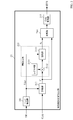
- FIG. 1 is a schematic configuration diagram of a video signal processing apparatus 1000 according to a first embodiment.
- FIG. 3 is a schematic configuration diagram of an estimated vertical synchronization signal generation unit 21 of the video signal processing apparatus 1000.
- 4 is a timing chart when an estimated vertical synchronization signal EVS is generated in the video signal processing apparatus 1000. The figure which showed typically image Img1 formed of a video signal. The timing chart in the case of producing
- FIG. 1 is a schematic configuration diagram of a video signal processing apparatus 1000 according to the first embodiment.
- FIG. 1 is a schematic configuration diagram of the video signal processing apparatus 1000 when processing a video signal in the DE mode (data enable mode).
- the video signal is processed in the SYNC mode (synchronous mode) or the SYNC-DE mode. The connection etc. when doing so are omitted.
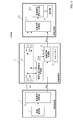
- FIG. 2 is a schematic configuration diagram of the estimated vertical synchronization signal generation unit 21 of the video signal processing apparatus 1000.
- the video signal processing apparatus 1000 includes a video receiving unit 1, a video processing unit 2, and a display control unit 3.
- the video receiver 1 includes a broadcast receiver 11 and a received signal processor 12 as shown in FIG.
- the broadcast receiving unit 11 receives a broadcast wave of a television signal, for example, and outputs the received broadcast wave (signal) to the received signal processing unit 12.
- the received signal processing unit 12 receives a signal output from the broadcast receiving unit 11, performs a demodulation process on the input signal, and acquires a baseband video signal. The reception signal processing unit 12 then outputs the acquired baseband video signal to the video processing unit 2 as a video signal Din.
- the reception signal processing unit 12 generates a clock signal (main clock signal) CLK and a data enable signal DE for processing the acquired baseband video signal, and generates the generated clock signal CLK and the data enable signal DE as a video. Output to the processing unit 2.
- the video processing unit 2 includes an interface unit 20, an estimated vertical synchronization signal generation unit 21, a video signal processing unit 22, and a line memory 23.
- the interface unit 20 includes an input buffer 201 for the clock signal CLK, an input buffer 202 for the data enable signal DE, an output buffer 203 for the clock signal CLK, and an output for the data enable signal DE.
- a buffer 204 is shown in FIG. 1, the interface unit 20.
- the input buffer 201 for the clock signal CLK is, for example, a buffer having a high input impedance and a low output impedance, and receives the clock signal CLK output from the reception signal processing unit 12.
- the input buffer 201 outputs the input clock signal CLK to the estimated vertical synchronization signal generation unit 21, the video signal processing unit 22, and the output buffer 203.
- the input buffer 202 for the data enable signal DE is, for example, a buffer having a high input impedance and a low output impedance, and receives the data enable signal DE output from the reception signal processing unit 12.
- the input buffer 202 outputs the input data enable signal DE to the estimated vertical synchronization signal generation unit 21, the video signal processing unit 22, and the output buffer 204.
- the clock signal CLK output buffer 203 is, for example, a buffer having a high input impedance and a low output impedance, and receives the clock signal CLK output from the input buffer 201.
- the output buffer 203 outputs the input clock signal CLK to the timing control unit 31 of the display control unit 3.
- the output buffer 204 for the data enable signal DE is, for example, a buffer having a high input impedance and a low output impedance, and receives the data enable signal DE output from the input buffer 202.
- the output buffer 204 outputs the input data enable signal DE to the timing control unit 31 of the display control unit 3.
- a delay unit for timing adjustment may be provided in the clock signal line and / or the data enable signal line.
- the estimated vertical synchronization signal generation unit 21 includes an edge detection unit 211, a counting unit 212, a threshold generation unit 213, a comparison unit 214, and an EVS (Estimated Vertical Sync) acquisition unit 215. Prepare.
- the edge detection unit 211 receives the data enable signal DE output from the interface unit 20.
- the edge detection unit 211 detects the rising edge (or falling edge) of the input data enable signal DE, and outputs a signal indicating the detection result to the counting unit 212 and the storage unit 2133 as the edge detection signal Edet. To do.
- the counting unit 212 inputs the clock signal CLK output from the interface unit 20 and the edge detection signal Edet output from the edge detection unit 211.
- the counting unit 212 performs a counting process using the clock signal CLK. Specifically, the counting unit 212 (1) when the edge detection signal Edet is a signal value indicating that the rising edge (or falling edge) portion of the data enable signal DE has been detected, Reset (reset the count value to “0”), (2) In other cases, count processing by the clock signal CLK is executed. That is, the counting unit 212 counts the number of clocks of the clock signal CLK input to the counting unit 212.
- the counting unit 212 outputs the counted value as the count value C to the multiplier 2132 and the comparison unit 214.
- the threshold generation unit 213 includes a register unit 2131, a multiplier 2132, and a storage unit 2133.
- the register unit 2131 holds information on the coefficient k to be multiplied by the count value C in the multiplier 2132.
- the coefficient k held in the register unit 2131 may be changeable by an external command.
- the register unit 2131 outputs the retained coefficient k to the multiplier 2132.
- the multiplier 2132 receives the count value C output from the counting unit 212 and the coefficient k output from the register unit 2131. Multiplier 2132 multiplies count value C by coefficient k, and outputs the multiplication result (k ⁇ C) to storage unit 2133.
- the storage unit 2133 receives the multiplication result (k ⁇ C) output from the multiplier 2132 and the edge detection signal Edet output from the edge detection unit 211.
- the storage unit 2133 stores a multiplication result (k ⁇ C) when the edge detection signal Edet is a signal value indicating that the rising edge (or falling edge) portion of the data enable signal DE is detected.
- the storage unit 2133 the multiplication result stored in the last time (k ⁇ C), as a threshold S n, and outputs to the comparing unit 214.
- Comparing unit 214 inputs the count value C output from the counter 212, and a threshold value S n is output from the storage unit 2133 of the threshold generator 213. Comparing unit 214 compares the count value C with the threshold value S n, and outputs a signal indicating the comparison result to the EVS acquisition unit 215.
- the EVS acquisition unit 215 receives a signal indicating the comparison result from the comparison unit 214.
- the EVS acquisition unit 215 indicates that the signal indicates C ⁇ S n from the signal value indicating that C ⁇ S n (for example, the signal value “0”).
- a signal obtained by activating the signal value only for a predetermined period for example, a period of one clock cycle
- EVS the estimated vertical synchronization signal
- the video signal processing unit 22 inputs the video signal Din output from the reception signal processing unit 12 of the video reception unit 1 and the estimated vertical synchronization signal EVS output from the estimated vertical synchronization signal generation unit 21. Further, the video signal processing unit 22 receives the clock signal CLK output from the interface unit 20 and the data enable signal DE. The video signal processing unit 22 performs, for example, horizontal video signal processing on the video signal Din using the clock signal CLK, the data enable signal DE, and the estimated vertical synchronization signal EVS. Then, the video signal processing unit 22 outputs the video signal after the video signal processing to the display control unit 3 as a video signal Dout.
- the video signal processing unit 22 is connected to the line memory 23 as shown in FIG.
- the video signal processing unit 22 may appropriately store the video signal in the line memory 23 and execute the predetermined video signal processing.
- the line memory 23 may be provided inside the video signal processing unit 22.
- the line memory 23 is connected to the video signal processing unit 22, and based on a command from the video signal processing unit 22, a predetermined video signal (for example, N lines (N: natural number)) Video data). Further, the line memory 23 outputs the stored video signal (video data) to the video signal processing unit 22 based on an instruction from the video signal processing unit 22.
- a predetermined video signal for example, N lines (N: natural number)
- Video data for example, N lines (N: natural number)
- the line memory 23 outputs the stored video signal (video data) to the video signal processing unit 22 based on an instruction from the video signal processing unit 22.
- the display control unit 3 includes a timing control unit 31 and a display panel drive unit 32 as shown in FIG.
- the timing control unit 31 inputs the clock signal CLK and the data enable signal DE output from the video processing unit 2 and the video signal Dout output from the video signal processing unit 22.
- the timing control unit 31 generates a drive signal for displaying a video signal on a display panel (not shown) based on the clock signal CLK and the data enable signal DE.
- the timing control unit 31 then outputs the generated drive signal to the display panel drive unit 32 together with the video signal (video data) to be displayed on the display panel.
- the display panel drive unit 32 inputs a drive signal and a video signal (video data) output from the timing control unit 31.
- the display panel drive unit 32 displays the video signal on the display panel by driving the display panel based on the drive signal (for example, by driving the gate line and the source line of the display panel).
- the video signal processing apparatus 1000 may include a display panel (not shown) that displays a video signal under the control of the display control unit 3.
- the display panel is realized by a liquid crystal display panel, for example.
- a broadcast wave of a television signal is received, and the received broadcast wave (signal) is output to the received signal processor 12.
- the reception signal processing unit 12 performs demodulation processing or the like on the signal output from the broadcast reception unit 11 to acquire a baseband video signal Din.
- the acquired baseband video signal Din is output to the video signal processing unit 22 of the video processing unit 2.
- the reception signal processing unit 12 generates a clock signal (main clock signal) CLK and a data enable signal DE for processing the acquired baseband video signal.
- the generated clock signal CLK and data enable signal DE are output to the video processing unit 2.
- the estimated vertical synchronization signal generation unit 21 of the video processing unit 2 generates an estimated vertical synchronization signal EVS based on the clock signal CLK and the data enable signal DE output from the reception signal processing unit 12.
- FIG. 3 is a timing chart when the estimated vertical synchronization signal EVS is generated in the video signal processing apparatus 1000. Specifically, in FIG. 3, the data enable signal DE, the estimated vertical synchronization signal EVS, the count value C output from the counting unit 212, and the threshold value output from the threshold generation unit 213 are matched with the time axis. shows and S n, a.
- the edge detection unit 211 detects a rising edge of the data enable signal DE and outputs an edge detection signal Edet indicating the detection result to the counting unit 212.
- the count value C is output from the counting unit 212 to the multiplier 2132 of the threshold value generating unit 213.
- the coefficient k output from the register unit 2131 and the count value C are multiplied. Then, the multiplication result (C ⁇ k) is output to the storage unit 2133.
- k 2 is described below.
- the EVS acquisition unit 215 sets the signal value of the estimated vertical synchronization signal EVS to a value indicating inactivity (this embodiment In the embodiment, this value is set to “0”) and is output to the video signal processing unit 22.
- time t1 to t2 At time t1, the edge detection unit 211 detects a rising edge of the data enable signal DE and outputs an edge detection signal Edet indicating the detection result to the counting unit 212.
- the multiplier 2132 the coefficient k output from the register unit 2131 and the count value C are multiplied. Then, the multiplication result (C ⁇ k) is output to the storage unit 2133.
- the EVS acquisition unit 215 sets the signal value of the estimated vertical synchronization signal EVS to a value “0” indicating that it is inactive. Is output to the video signal processing unit 22.
- time t3 to t4 In the period from time t3 to t4, as shown in FIG. 3, the period from time t_bts to t4 is the blanking period of data enable signal DE (period BT shown in FIG. 3).
- the blanking period of the data enable signal DE is shown as a period corresponding to about 2H (two lines of the video signal). May be longer. Further, the blanking period of the data enable signal DE may be a period corresponding to a vertical blanking period such as an NTSC television signal.
- the edge detection unit 211 detects a rising edge of the data enable signal DE and outputs an edge detection signal Edet indicating the detection result to the counting unit 212.
- the counting unit 212 resets the count value to “0” at time t3 based on the edge detection signal Edet. Then, each time the clock signal CLK is input (for example, every time a rising edge of the clock signal is detected) in the period from time t3 to t4, the count value is incremented by “+1” to perform the count process. Execute.
- the indicated value “0” is output to the EVS acquisition unit 215.
- the EVS acquisition unit 215 deactivates the signal value of the estimated vertical synchronization signal EVS. Is output to the video signal processing unit 22 as a value “0” indicating that the
- the EVS acquisition unit 215 detects that the value output from the comparison unit 214 has changed from “0” to “1” at time t_evs, and indicates that the signal value of the estimated vertical synchronization signal EVS is active Set to “1” and output to the video signal processing unit 22.
- the EVS acquisition unit 215 detects that the value output from the comparison unit 214 has changed from “0” to “1”, for example, the EVS acquisition unit 215 sets the signal value of the estimated vertical synchronization signal EVS for one clock cycle. Only the value “1” indicating that it is active is output to the video signal processing unit 22.
- the timing at which the signal value of the estimated vertical synchronization signal EVS becomes active is time t_evs, which is 2 ⁇ (time t2 to t3) from time t3 when the rising edge of the data enable signal DE is detected. ) Time has elapsed.
- the average clock period of the estimated vertical timing signal value becomes active synchronizing signal EVS from time t3, the time t2 to twice the value of the clock count number T 3 in ⁇ t3, the time t2 the clock signal CLK at ⁇ t3 Is the time when the time corresponding to the value multiplied by.
- the EVS acquisition unit 215 changes the output value from the comparison unit 214. Therefore, the signal value of the estimated vertical synchronization signal EVS is output to the video signal processing unit 22 as a value “0” indicating that it is inactive.
- the threshold value S 4 2T 4 is set, and T 4 is a large value, so the threshold value S 4 is also set to a large value.
- the count value C does not exceed the threshold value S 4.
- the signal value of the estimated vertical synchronization signal EVS becomes active only at time t_evs when the output value from the comparison unit 214 changes during the period from time t3 to t4.
- the estimated vertical synchronization signal EVS has an average clock of the clock signal CLK from time t2 to t3 to a value twice the clock count number T3 from time t2 to t3 from time t3 when the rising edge of the data enable signal DE is detected. It becomes active at the time when the time corresponding to the value multiplied by the period has elapsed.
- the estimated vertical synchronization signal generation unit 21 executes the above processing, so that even if there is no vertical synchronization signal, the blanking period ( An estimated vertical synchronization signal can be generated at a time (time t_evs) close to the start time of the vertical blanking period (the signal value of the estimated vertical synchronization signal EVS can be activated).
- the estimated vertical synchronization signal generation unit 21 of the video processing unit 2 performs estimation based on the clock signal CLK and the data enable signal DE input from the reception signal processing unit 12 and input through the interface unit 20.
- a vertical synchronization signal EVS is generated.
- the generated estimated vertical synchronization signal EVS is output to the video signal processing unit 22.
- the video signal processing unit 22 for example, vertical video signal processing is performed on the video signal Din using the estimated vertical synchronization signal EVS generated by the estimated vertical synchronization signal generation unit 21.
- the time when the signal value of the estimated vertical synchronization signal EVS becomes active corresponds to the blanking period (vertical blanking period) of the data enable signal DE. Since the time (time t_evs in the case of FIG. 3) is close to the start time of the (period), the required line memory capacity can be reduced.
- the estimated vertical synchronization signal EVS can quickly detect the blanking period of the data enable signal DE (a period corresponding to the vertical blanking period), the data enable signal DE is stored before the blanking period is detected.
- the number of lines of the video signal to be held can be reduced. For example, when video processing at the lower end of the screen is executed, a video signal having a predetermined number of lines must be stored and held until a blanking period (a period corresponding to the vertical blanking period) of the data enable signal DE is detected. Even in such a case, the blanking period (a period corresponding to the vertical blanking period) of the data enable signal DE can be quickly detected by the estimated vertical synchronization signal EVS. Memory capacity can be reduced.
- the video signal processing unit 22 can detect the blanking period (a period corresponding to the vertical blanking period) of the data enable signal DE based on the time when the estimated vertical synchronization signal EVS becomes active, and the detection time thereof. Based on the above, by counting the rising edges of the data enable signal DE, it is possible to grasp what line the signal in the frame is the video signal to be processed. Thereby, the video signal processing unit 22 can appropriately execute the video signal processing in the vertical direction by the estimated vertical synchronization signal EVS even when there is no vertical synchronization signal.
- the blanking period a period corresponding to the vertical blanking period
- the video signal Dout subjected to the video signal processing by the video signal processing unit 22 is output to the timing control unit 31 of the display control unit 3.
- the timing control unit 31 of the display control unit 3 generates a drive signal for displaying the video signal Dout on the display panel based on the clock signal CLK and the data enable signal DE. Then, the generated drive signal is output to the display panel drive unit 32 together with the video signal Dout.
- the display panel drive unit 32 drives the display panel based on the drive signal generated by the timing control unit 31 so that the video signal Dout is displayed on the display panel. As a result, an image formed by the image signal Dout is displayed on the display panel.
- the threshold value S n k ⁇ T n in the period (t n + 1 ) is set.
- the signal value of the estimated vertical synchronization signal EVS is activated. Therefore, in the video signal processing apparatus 1000, even when there is no vertical synchronization signal, a time (for example, as shown in FIG. 3) close to the start time of the blanking period (a period corresponding to the vertical blanking period) of the data enable signal DE. At time t_evs), an estimated vertical synchronization signal can be generated (the signal value of the estimated vertical synchronization signal EVS can be activated).
- the video signal processing apparatus 1000 uses the estimated vertical synchronization signal EVS generated as described above, for example, to perform vertical video signal processing, thereby reducing the required line memory capacity. However, appropriate video signal processing can be executed.
- the video signal processing apparatus 1000 does not detect the blanking period (a period corresponding to the vertical blanking period) of the data enable signal DE using a fixed threshold value. Even if the signal or the like changes, it is possible to generate the estimated vertical synchronization signal EVS that appropriately detects the blanking period (a period corresponding to the vertical blanking period) of the data enable signal DE.
- a spread spectrum clock signal may be used to suppress electromagnetic radiation (EMI). In such a case, the number of clocks in one horizontal period may vary from line to line. . Even in such a liquid crystal television or the like, by applying the video signal processing apparatus 1000, the estimated vertical synchronization signal EVS can be appropriately generated even when the number of clocks varies.
- the number of lines in one frame may be slightly changed to synchronize the input video signal with the output liquid crystal panel (display panel).
- the signal processing apparatus 1000 the estimated vertical synchronization signal EVS can be appropriately generated.
- the video signal processing apparatus 1000 can perform vertical video signal processing using the estimated vertical synchronization signal EVS generated as described above, when there is no vertical synchronization signal, or estimation is performed. When there is no vertical synchronization signal, video processing that could not be properly processed can be appropriately processed.
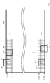
- FIG. 4 is a diagram schematically showing an image Img1 formed by the video signal.
- the image Img1 has 1920 pixels in the horizontal direction and 1080 pixels in the vertical direction.
- FIG. 4 a part of the image area from the first line L1 to the fifth line L5 of the image Img1, and the image area from the 1076th line L1076 to the 1080th line L1080 of the image Img1. Some are shown.
- the filter process is executed with a 5 ⁇ 5 filter coefficient
- a 5 ⁇ 5 filter is obtained even if there is no vertical synchronization signal or estimated vertical synchronization signal Since the target pixel (5 pixels ⁇ 5 pixels) to be multiplied by the coefficient is present around the target pixel, the filtering process is appropriately executed.
- the pixel P1 or the pixel P4 shown in FIG. 4 is set as a processing target (target pixel) and filter processing is performed using a 5 ⁇ 5 filter coefficient
- the target pixel (5 pixels ⁇ 5 ⁇ 5 ⁇ 5) is multiplied by the 5 ⁇ 5 filter coefficient. 5 pixels) does not exist in the vicinity of the target pixel, and therefore, the filter process is not appropriately executed.
- the pixel P1 shown in FIG. 4 is a processing target (target pixel)
- inappropriate filtering is performed with the area AR1 shown in FIG. 4 as a filtering target.
- the data for two lines above the pixel P1 (data for 10 pixels)
- Filter processing is performed using the data for the bottom two lines of the image one frame before held in the line memory (the data of the 1079th line and the data of the 1080th line of the image one frame before). It will be executed.
- the video signal processing apparatus 1000 can generate the estimated vertical synchronization signal EVS even when there is no vertical synchronization signal, and the video signal processing unit 22 uses the estimated vertical synchronization signal EVS to process the pixel to be processed. It is possible to appropriately grasp which line the pixel is included in. That is, in the video signal processing apparatus 1000, it can be seen that the pixel P1 is a pixel included in the first line by the estimated vertical synchronization signal EVS even when there is no vertical synchronization signal. Therefore, in the video signal processing apparatus 1000, for example, when the pixel to be processed is the pixel P1 and the filtering process using the 5 ⁇ 5 filter coefficient is performed, it is determined that there is no data for two lines above the pixel P1, and an exception is made.
- Processing for example, filter processing using 15 pixels of the first to third lines included in the area AR1 can be performed.
- data for executing video signal processing for example, filter processing using a 5 ⁇ 5 filter coefficient
- the pixel P1 is a processing target pixel. Even in such a case, it is possible to appropriately prevent inappropriate video signal processing from being executed.
- the pixel P4 shown in FIG. 4 is a processing target (target pixel)
- inappropriate filtering is performed with the area AR4 shown in FIG. 4 as the filtering target. End up. That is, when filtering is performed on the pixel P4 on the 1080th line, if there is no vertical synchronization signal or estimated vertical synchronization signal, the data for two lines below the pixel P4 (data for 10 pixels) Filter processing is executed using data for the uppermost two lines of the image after one frame (the data of the first line and the data of the second line of the image after one frame).
- the video signal processing apparatus 1000 can generate the estimated vertical synchronization signal EVS even when there is no vertical synchronization signal, and the video signal processing unit 22 uses the estimated vertical synchronization signal EVS to process the pixel to be processed. It is possible to appropriately grasp which line the pixel is included in. That is, in the video signal processing apparatus 1000, it can be seen that the pixel P4 is a pixel included in the 1080th line by the estimated vertical synchronization signal EVS even when there is no vertical synchronization signal. Therefore, in the video signal processing apparatus 1000, for example, when the pixel to be processed is the pixel P4 and the filter processing is performed with the 5 ⁇ 5 filter coefficient, it is determined that there is no data for two lines below the pixel P4, and an exception is made.
- Processing for example, filter processing using 15 pixels of the 1078th to 1080th lines included in the area AR4.
- data for executing video signal processing for example, filter processing using a 5 ⁇ 5 filter coefficient
- the pixel P4 is set as a processing target pixel. Even in such a case, it is possible to appropriately prevent inappropriate video signal processing from being executed.
- the video signal processing apparatus 1000 can execute the video signal processing in the vertical direction by using the estimated vertical synchronization signal EVS generated by the estimated vertical synchronization signal generation unit 21, and thus there is no vertical synchronization signal. In this case, or when there is no estimated vertical synchronization signal, video processing that could not be properly processed can be appropriately processed.
- the edge detection unit 211 of the estimated vertical synchronization signal generation unit 21 of the video signal processing apparatus 1000 of the first embodiment the rising edge of the data enable signal DE is detected, but the edge detection of the video signal processing apparatus of this modification example
- the unit 211 detects the falling edge of the data enable signal DE, and activates the edge detection signal Edet when the falling edge is detected.
- the video signal processing apparatus of the present modification is the same as the video signal processing apparatus 1000 of the first embodiment.
- FIG. 5 is a timing chart when the estimated vertical synchronization signal EVS is generated in the video signal processing device of the present modification. Specifically, in FIG. 5, as in FIG. 3, the time axes are matched, the data enable signal DE, the estimated vertical synchronization signal EVS, the count value C output from the counting unit 212, and the threshold generation unit It shows a threshold value S n output from 213.
- the count value C output from the counting unit 212 is counted from the time when the falling edge of the data enable signal DE is detected.
- the timing at which the signal value of the estimated vertical synchronization signal EVS becomes active is time t_evs, and the falling edge of the data enable signal DE is detected. This is the time when 2 ⁇ (time from t2 to t3) has elapsed since time t3.
- the timing at which the signal value of the estimated vertical synchronizing signal EVS becomes active from time t3, the value of twice the clock count number T 3 at time t2 ⁇ t3 (k times), the clock signal at time t2 ⁇ t3 CLK This is the time when the time corresponding to the value obtained by multiplying the average clock period has elapsed. In FIG. 5, this is shown as “2TT 3 ” (period corresponding to the clock count number 2T 3 minutes of the clock signal CLK) in the period from time t3 to t_evs.
- the blanking period (vertical) of the data enable signal DE is obtained even when there is no vertical synchronization signal.
- the estimated vertical synchronization signal can be generated (the signal value of the estimated vertical synchronization signal EVS can be activated) at a time (for example, time t_evs in FIG. 5) close to the start time of the blanking period. it can).
- FIG. 6 shows a schematic configuration diagram of the estimated vertical synchronization signal generation unit 21A of the present modification.
- the video signal processing device of this modification has a configuration in which the estimated vertical synchronization signal generation unit 21 is replaced with the estimated vertical synchronization signal generation unit 21A in the video signal processing device 1000 of the first embodiment.
- the video signal processing apparatus of the present modification is the same as the video signal processing apparatus 1000 of the first embodiment.
- the estimated vertical synchronization signal generation unit 21A has a configuration in which the threshold generation unit 213 is replaced with a threshold generation unit 213A in the estimated vertical synchronization signal generation unit 21 of the first embodiment.
- the threshold generation unit 213A has a configuration in which the positions of the register unit 2131, the multiplier 2132, and the storage unit 2133 are exchanged in the threshold generation unit 213.
- the storage unit 2133 stores the count value C output from the counting unit 212 at the timing when the edge detection signal Edet becomes active.
- the video signal processing apparatus of the present modification can also execute the same processing as in the first embodiment.
- edge detection unit 211 of the present modification may also detect a falling edge, as in the first modification of the first embodiment.
- FIG. 7 shows a schematic configuration diagram of a video signal processing apparatus 1000A of the present modification.
- the video signal processing apparatus 1000A has a configuration in which the video receiving unit 1 is replaced with a video input unit 1A in the video signal processing apparatus 1000 of the first embodiment.
- the video input unit 1A includes a video signal input unit 11A and an input signal processing unit 12A.
- the video signal input unit 11A inputs a video signal output from, for example, a video playback device ex1 (for example, a DVD player, a BD player, an HDD playback device, etc.).
- the video signal output from the video playback device ex1 is a signal that complies with, for example, a communication interface standard (for example, HDMI or IEEE 1394).
- the video signal input unit 11A converts the input video signal into a baseband video signal, and outputs the converted video signal to the input signal processing unit 12A.
- the input signal processing unit 12A receives the baseband video signal output from the video signal input unit 11A.
- the input signal processing unit 12A outputs the input baseband video signal to the video signal processing unit 22 of the video processing unit 2 as a video signal Din.
- the input signal processing unit 12A generates a clock signal CLK and a data enable signal DE for processing the baseband video signal input from the video signal input unit 11A, and the generated clock signal CLK and data enable signal DE. Is output to the interface unit 20 of the video processing unit 2.
- an estimated vertical synchronization signal (estimated vertical synchronization signal) can be generated at a time close to the start time of the blanking period (a period corresponding to the vertical blanking period) of the data enable signal.
- the video signal processing apparatus 1000A executes vertical video signal processing using the estimated vertical synchronization signal EVS generated by the estimated vertical synchronization signal generation unit 21. Therefore, when there is no vertical synchronization signal or when there is no estimated vertical synchronization signal, video processing that could not be properly processed can be appropriately processed.
- FIG. 8 shows a schematic configuration diagram of a video signal processing apparatus 1000B according to this modification.
- the video signal processing apparatus 1000B has a configuration in which the display control unit 3 is replaced with a video recording unit 3A in the video signal processing apparatus 1000 of the first embodiment.
- the video recording unit 3A includes a video signal conversion unit 31A, a video signal writing unit 32A, and a recording unit 33.
- the video signal conversion unit 31A receives the clock signal CLK, the data enable signal DE, and the video signal Dout output from the video processing unit 2. Based on the clock signal CLK and the data enable signal DE, the video signal conversion unit 31A performs processing (for example, compression encoding processing) for converting the video signal Dout into a signal for writing to the recording unit 33 (for example, recording medium). Execute to generate data for writing. Then, the video signal conversion unit 31A outputs the generated write data to the video signal writing unit 32A.
- processing for example, compression encoding processing
- the video signal writing unit 32A receives the write data output from the video signal conversion unit 31A and writes the input write data to the recording unit 33 (for example, a recording medium).
- the recording unit 33 is, for example, a recording medium (for example, a hard disk, a flash memory, a magneto-optical disk, a large capacity DVD, a next generation DVD, a semiconductor memory, etc.).
- a recording medium for example, a hard disk, a flash memory, a magneto-optical disk, a large capacity DVD, a next generation DVD, a semiconductor memory, etc.
- data from the video signal writing unit 32A is written according to the control of the video signal writing unit 32A.
- the recording unit 33 may be a recording medium that can be detached from the video recording unit 3A.
- the processing of the video receiving unit 1 and the video processing unit 2 of the video signal processing apparatus 1000B of the present modification is the same as that in the above-described embodiment (including the modification).
- the blanking period of the data enable signal (corresponding to the vertical blanking period) is based on the data enable signal.
- the estimated vertical synchronization signal (estimated vertical synchronization signal) can be generated at a time close to the start time of (period).
- the video signal Dout processed using the estimated vertical synchronization signal can be recorded in the recording unit 33 by the video recording unit 3A.
- the video signal processing in the vertical direction is executed using the estimated vertical synchronization signal EVS generated by the estimated vertical synchronization signal generation unit 21. Therefore, when there is no vertical synchronization signal or when there is no estimated vertical synchronization signal, video processing that could not be properly processed can be appropriately processed.
- the coefficient k set in the register unit 2131 has been described as a fixed value.
- the present invention is not limited to this, and the coefficient k set in the register unit 2131 is a variable value. It may be. Further, the value of k may be a value other than “2” exemplified above. By adjusting the value of k, the timing at which the estimated vertical synchronization signal EVS becomes active can be adjusted. Also, the register unit 2131 that can change the value may be omitted, and the coefficient k may be a fixed value such as “2”.
- the reception signal processing unit 12 of the video reception unit 1 is realized by a system LSI
- the timing control unit 31 of the display control unit 3 is realized by another LSI (or IC)
- another LSI for example,
- the video signal processing apparatus may be configured by inserting the video processing unit 2 (as shown in FIG. 1). In this way, for example, in the apparatus in which the reception signal processing unit 12 of the video reception unit 1 and the timing control unit 31 are directly connected, the video processing unit 2 is added, and the output video of the reception signal processing unit 12 With respect to the signal, the video signal after the video processing by the estimated vertical synchronization signal EVS can be input to the timing control unit 31.
- the function e.g., estimated vertical synchronization
- Video signal processing in the vertical direction using the signal EVS can be realized.
- various configurations are possible. The present invention can be applied to any of them.
- the configuration in which the clock signal CLK and the data enable signal DE are supplied from the video receiving unit 1 to the timing control unit 31 via the video processing unit 2 has been described.
- the delay process or the like is not clearly shown, but the data enable signal DE is subjected to the delay process in the video processing unit 2 or the like and supplied to the timing control unit 31 as necessary. It may be (output).
- the clock signal CLK and the data enable signal DE may be directly supplied (output) from the reception signal processing unit 12 to the video processing unit 2 and the timing control unit 31. Further, the clock signal CLK and the data enable signal DE may be generated by a function unit other than the reception signal processing unit 12.
- the video signal processing apparatus may be realized by combining a part or all of the above-described embodiments (including modifications). Further, the estimated vertical synchronization signal generation unit 21 may be configured as a single device.
- a display panel may be realized by adding a display panel to the video signal processing apparatus of the above-described embodiment (including the modified example).
- a part or all of the video signal processing apparatus of the above embodiment may be realized as an integrated circuit (for example, an LSI, a system LSI, etc.).
- Part or all of the processing of each functional block in the above embodiment may be realized by a program. And a part or all of the processing of each functional block of the above embodiment may be executed by a central processing unit (CPU) in the computer.
- a program for performing each processing is stored in a storage device such as a hard disk or ROM, and a central processing unit (CPU) reads the program from the ROM or RAM and executes it. Also good.
- each process of the above embodiment may be realized by hardware, or may be realized by software (including a case where it is realized together with an OS (operating system), middleware, or a predetermined library). Further, it may be realized by mixed processing of software and hardware.
- OS operating system
- middleware middleware
- predetermined library predetermined library
- an input buffer and an output buffer may be provided in each functional unit of the above-described embodiment (including the modified example).
- execution order of the processing methods in the above embodiment is not necessarily limited to the description of the above embodiment, and the execution order can be changed without departing from the gist of the invention.
- a computer program that causes a computer to execute the above-described method and a computer-readable recording medium that records the program are included in the scope of the present invention.
- the computer-readable recording medium include a flexible disk, a hard disk, a CD-ROM, an MO, a DVD, a large-capacity DVD, a next-generation DVD, and a semiconductor memory.
- the computer program is not limited to the one recorded on the recording medium, but may be transmitted via a telecommunication line, a wireless or wired communication line, a network represented by the Internet, or the like.
- the video signal processing apparatus of the first configuration is a video signal processing apparatus that receives at least a clock signal, a data enable signal, and an image signal and outputs at least a clock signal, a data enable signal, and a processed image signal. And an interface unit, an estimated vertical synchronization signal generation unit, and a video signal processing unit.
- the interface unit inputs a clock signal and a data enable signal, and outputs a clock signal and a data enable signal.
- the estimated vertical synchronization signal generator generates an estimated vertical synchronization signal based on the clock signal and the data enable signal.
- the video signal processing unit receives the image signal, generates a processed image signal by performing a predetermined process on the image signal using the estimated vertical synchronization signal generated by the estimated vertical synchronization signal generation unit, and generates the processed image signal
- the processed image signal is output.
- the estimated vertical synchronization signal generation unit generates an estimated vertical synchronization signal based on the clock signal and the data enable signal, and the video signal processing unit generates the estimated vertical synchronization signal generated by the estimated vertical synchronization signal generation unit.
- a predetermined process is performed on the image signal using the signal. Therefore, in this video signal processing device, video signal processing can be appropriately executed using the estimated vertical synchronization signal even when there is no vertical synchronization signal.
- the video signal processing device of the second configuration is the first configuration, wherein the estimated vertical synchronization signal generation unit includes an edge detection unit, a counting unit, a threshold generation unit, a comparison unit, an estimated vertical synchronization signal acquisition unit, .
- the edge detection unit detects either the rising edge or the falling edge of the data enable signal.
- the counting unit counts the number of clock signals in a time period from time t n when the edge detection unit detects the edge to time t n + 1 when the edge detection unit detects the edge.
- Threshold generating part is a time at which the edge detecting unit detects an edge, a time before the time t n, and, during the most from near the time t n-1 at time t n to the time point t n
- a value (T n ⁇ k) obtained by multiplying the count value T n of the number of clocks counted by the counting unit and the coefficient k is set as the threshold value Sn.
- the comparison unit compares the threshold value Sn with the count value of the number of clocks counted by the counting unit.
- the estimated vertical synchronization signal acquisition unit when the comparison unit detects that the magnitude relationship between the threshold value Sn and the count value of the number of clocks counted by the counting unit has changed, estimates vertical synchronization signal that activates the signal value Generate a signal.
- the number of clocks in the period (between time t n-1 to t n ) between the edges of the data enable signal DE (between either the rising edge or the falling edge) is counted.
- the value obtained by multiplying the count value by the coefficient k is set as the threshold value Sn in the period between the edges of the next data enable signal DE (the period from time t n to t n + 1 ).
- the count value of the number of clocks is compared with the threshold value Sn during the period of time t n to t n + 1 , and when the magnitude relationship between the count value and the threshold value Sn changes, the estimated vertical synchronization
- the signal value of the signal EVS is activated.
- the estimated vertical synchronization signal is displayed at a time close to the start time of the blanking period (a period corresponding to the vertical blanking period) of the data enable signal.
- the signal value of the estimated vertical synchronization signal EVS can be activated.
- the estimated vertical synchronizing signal (estimated vertical synchronizing signal) can be generated.
- the magnitude relationship between the threshold value Sn and the count value of the number of clocks counted by the counting unit changes is, for example, (1) a state where Sn> count value (or Sn ⁇ count value).
- the signal value of the estimated vertical synchronization signal becomes active.
- the edge detection unit (1) detects only the rising edge when detecting the rising edge, and (2) detects only the falling edge when detecting the falling edge. That is, the edge detection unit does not detect both the rising edge and the falling edge. Note that the edge detection unit may detect a position shifted by a predetermined time from the rising edge (or falling edge).
- the threshold value generation unit sets the threshold value Sn with a coefficient of “2”.
- the time when the edge (for example, the rising edge) is detected last before the blanking period of the data enable signal starts is set as time t3, and the edge is detected once before time t3.
- the time at which (for example, the rising edge) is detected is time t2
- the time 2 ⁇ time from t2 to t3 has elapsed since the time t3 at which the edge of the data enable signal (for example, the rising edge) was detected.
- the signal value of the estimated vertical synchronization signal is activated.
- the timing at which the signal value of the estimated vertical synchronization signal becomes active is changed from time t3 to a value twice (k times) the number of clock counts at times t2 to t3.
- the time corresponding to the value obtained by multiplying the average clock period of the clock signal at has elapsed. Therefore, in this video signal processing device, it is possible to generate the estimated vertical synchronization signal (estimated vertical synchronization signal) at a time close to the start time of the blanking period (a period corresponding to the vertical blanking period) of the data enable signal. it can.
- the video signal processing unit performs at least video signal processing in the vertical direction.
- video signal processing including at least vertical video signal processing can be appropriately executed using the estimated vertical synchronization signal.
- the present invention even when there is no vertical synchronizing signal, the estimated vertical at a time close to the start time of the blanking period (a period corresponding to the vertical blanking period) of the data enable signal based on the data enable signal.
- a synchronization signal (estimated vertical synchronization signal) can be generated. Therefore, the present invention is useful in the video related industry field and can be implemented in this field.
- Video signal processing device 1 Video receiving unit 2 Video processing unit 21, 21A Estimated vertical synchronization signal generating unit 211 Edge detecting unit 212 Counting unit 213, 213A Threshold generating unit 214 Comparison unit 215 EVS acquisition unit (estimated vertical synchronization Signal acquisition unit) 22 Video signal processor (video processor) 3 Display controller
Landscapes
- Engineering & Computer Science (AREA)
- Multimedia (AREA)
- Physics & Mathematics (AREA)
- Computer Hardware Design (AREA)
- General Physics & Mathematics (AREA)
- Theoretical Computer Science (AREA)
- Signal Processing (AREA)
- Control Of Indicators Other Than Cathode Ray Tubes (AREA)
Abstract
映像処理部(2)は、少なくともクロック信号、データイネーブル信号、および、画像信号を入力とし、少なくともクロック信号、データイネーブル信号、および、処理後画像信号を出力とする。映像処理部(2)は、インターフェース部(20)と、推定垂直同期信号生成部(21)と、映像信号処理部(22)と、を備える。インターフェース部(20)は、クロック信号と、データイネーブル信号とを入力するとともに、クロック信号と、データイネーブル信号とを出力する。推定垂直同期信号生成部(21)は、クロック信号及びデータイネーブル信号に基づき推定垂直同期信号を生成する。映像信号処理部(22)は、画像信号を入力し、推定垂直同期信号を用いて画像信号に所定の処理を実行することで処理後画像信号を生成し、生成した処理後画像信号を出力する。
Description
本発明は、垂直同期信号がない場合であっても、垂直同期信号を推定し、推定した垂直同期信号を用いて、映像信号処理を実行することができるようにするための技術に関する。
液晶テレビなどの表示装置では、映像信号を表示させる場合、(1)SYNCモード(同期モード)により映像信号を表示させる場合と、(2)SYNC-DEモードにより映像信号を表示させる場合と、(3)DEモード(データイネーブル・モード)により映像信号を表示させる場合と、がある。
SYNCモード(同期モード)により映像信号を表示させる場合、表示装置では、垂直同期信号、水平同期信号、メインクロック信号を用いて、映像信号(映像データ)を表示させる。また、SYNC-DEモードにより映像信号を表示させる場合、表示装置では、垂直同期信号、水平同期信号、データイネーブル信号、メインクロック信号を用いて、映像信号(映像データ)を表示させる。
一方、DEモードにより映像信号を表示させる場合、表示装置では、垂直同期信号および水平同期信号を用いることなく、データイネーブル信号と、メインクロック信号とを用いて、映像信号(映像データ)を表示させる。
DEモードの場合、垂直同期信号が存在しないため、入力される映像データが1フレーム中の何ライン目の映像データであるかを把握することができず、その結果、垂直方向の映像処理を適切に実行できない場合がある。
例えば、特許文献1(特許第4040712号公報)に開示されている技術では、DEモードにおいて、データイネーブル信号のブランキング期間に基づいて、所定のタイミングで、プレチャージSTV信号を生成する。そして、特許文献1に開示されている技術では、生成したプレチャージSTV信号により、実際のデータ(映像データ)が入力されるタイミングを示すメインSTV信号が入力される前に、表示パネルのゲートをオンさせる。これにより、特許文献1に開示されている技術では、ゲートの駆動速度を速くすることができる。つまり、特許文献1の技術では、垂直同期信号が存在しないDEモードにおいて、本来、垂直同期信号を基準にして決定していたタイミングを、データイネーブル信号に基づいて生成した信号(プレチャージSTV信号)により把握することができる。
しかしながら、上記特許文献1の技術は、データイネーブル信号のブランキング期間が終了するタイミングからクロックパルス垂直信号(CPV信号)2つ分だけ前のタイミング(ブランキング期間が終了する直前のタイミング)を検出することを前提としており、データイネーブル信号のブランキング期間の開始時刻に近い時刻に、垂直同期信号に相当する信号を発生させることは困難である。
そこで、本発明は、上記問題点に鑑み、垂直同期信号がない場合であっても、データイネーブル信号に基づいて、データイネーブル信号のブランキング期間(垂直帰線期間に相当する期間)の開始時刻に近い時刻において、推定した垂直同期信号(推定垂直同期信号)を発生させることができる映像信号処理装置を実現することを目的とする。
上記課題を解決するために、第1の構成の映像信号処理装置は、少なくともクロック信号、データイネーブル信号、および、画像信号を入力とし、少なくともクロック信号、データイネーブル信号、および、処理後画像信号を出力とする映像信号処理装置であって、インターフェース部と、推定垂直同期信号生成部と、映像信号処理部と、を備える。
インターフェース部は、クロック信号と、データイネーブル信号とを入力するとともに、クロック信号と、データイネーブル信号とを出力する。
推定垂直同期信号生成部は、クロック信号及びデータイネーブル信号に基づき推定垂直同期信号を生成する。
映像信号処理部は、画像信号を入力し、推定垂直同期信号生成部により生成された推定垂直同期信号を用いて画像信号に所定の処理を実行することで処理後画像信号を生成し、生成した処理後画像信号を出力する。
本発明によれば、垂直同期信号がない場合であっても、データイネーブル信号に基づいて、データイネーブル信号のブランキング期間(垂直帰線期間に相当する期間)の開始時刻に近い時刻において、推定した垂直同期信号(推定垂直同期信号)を発生させることができる映像信号処理装置を実現することができる。
[第1実施形態]
第1実施形態について、図面を参照しながら、以下、説明する。
第1実施形態について、図面を参照しながら、以下、説明する。
<1.1:映像信号処理装置の構成>
図1は、第1実施形態に係る映像信号処理装置1000の概略構成図である。なお、図1は、DEモード(データイネーブル・モード)により映像信号を処理する場合の映像信号処理装置1000の概略構成図であり、SYNCモード(同期モード)あるいはSYNC-DEモードにより映像信号を処理する場合の接続等を省略している。
図1は、第1実施形態に係る映像信号処理装置1000の概略構成図である。なお、図1は、DEモード(データイネーブル・モード)により映像信号を処理する場合の映像信号処理装置1000の概略構成図であり、SYNCモード(同期モード)あるいはSYNC-DEモードにより映像信号を処理する場合の接続等を省略している。
図2は、映像信号処理装置1000の推定垂直同期信号生成部21の概略構成図である。
映像信号処理装置1000は、図1に示すように、映像受信部1と、映像処理部2と、表示制御部3と、を備える。
映像受信部1は、図1に示すように、放送受信部11と、受信信号処理部12とを備える。
放送受信部11は、例えば、テレビジョン信号の放送波を受信し、受信した放送波(信号)を、受信信号処理部12に出力する。
受信信号処理部12は、放送受信部11から出力される信号を入力し、入力された信号に対して復調処理等を行い、ベースバンドの映像信号を取得する。そして、受信信号処理部12は、取得したベースバンドの映像信号を、映像信号Dinとして、映像処理部2に出力する。
また、受信信号処理部12は、取得したベースバンドの映像信号を処理するためのクロック信号(メインクロック信号)CLKおよびデータイネーブル信号DEを生成し、生成したクロック信号CLKおよびデータイネーブル信号DEを映像処理部2に出力する。
映像処理部2は、図1に示すように、インターフェース部20と、推定垂直同期信号生成部21と、映像信号処理部22と、ラインメモリ23と、を備える。
インターフェース部20は、図1に示すように、クロック信号CLKの入力用バッファ201と、データイネーブル信号DEの入力用バッファ202と、クロック信号CLKの出力用バッファ203と、データイネーブル信号DEの出力用バッファ204と、を備える。
クロック信号CLKの入力用バッファ201は、例えば、入力インピーダンスが高く、出力インピーダンスが低いバッファであり、受信信号処理部12から出力されたクロック信号CLKを入力する。入力用バッファ201は、入力したクロック信号CLKを、推定垂直同期信号生成部21と、映像信号処理部22と、出力用バッファ203とに出力する。
データイネーブル信号DEの入力用バッファ202は、例えば、入力インピーダンスが高く、出力インピーダンスが低いバッファであり、受信信号処理部12から出力されたデータイネーブル信号DEを入力する。入力用バッファ202は、入力したデータイネーブル信号DEを、推定垂直同期信号生成部21と、映像信号処理部22と、出力用バッファ204とに出力する。
クロック信号CLKの出力用バッファ203は、例えば、入力インピーダンスが高く、出力インピーダンスが低いバッファであり、入力用バッファ201から出力されたクロック信号CLKを入力する。出力用バッファ203は、入力したクロック信号CLKを、表示制御部3のタイミング制御部31に出力する。
データイネーブル信号DEの出力用バッファ204は、例えば、入力インピーダンスが高く、出力インピーダンスが低いバッファであり、入力用バッファ202から出力されたデータイネーブル信号DEを入力する。出力用バッファ204は、入力したデータイネーブル信号DEを、表示制御部3のタイミング制御部31に出力する。
なお、インターフェース部20において、タイミング調整用の遅延器を、クロック信号ライン、および/または、データイネーブル信号ラインに設けるようにしてもよい。
推定垂直同期信号生成部21は、図2に示すように、エッジ検出部211と、計数部212と、閾値生成部213と、比較部214と、EVS(Estimated Vertical Sync)取得部215と、を備える。
エッジ検出部211は、インターフェース部20から出力されるデータイネーブル信号DEを入力する。エッジ検出部211は、入力されたデータイネーブル信号DEの立ち上がりエッジ(または、立ち下がりエッジ)を検出し、検出結果を示す信号をエッジ検出信号Edetとして、計数部212と、記憶部2133とに出力する。
計数部212は、インターフェース部20から出力されるクロック信号CLKと、エッジ検出部211から出力されるエッジ検出信号Edetとを入力する。計数部212は、クロック信号CLKによるカウント処理を実行する。具体的には、計数部212は、(1)エッジ検出信号Edetが、データイネーブル信号DEの立ち上がりエッジ(または、立ち下がりエッジ)部分が検出されたことを示す信号値である場合、カウント値をリセットし(カウント値を「0」にリセットし)、(2)それ以外の場合は、クロック信号CLKによるカウント処理を実行する。つまり、計数部212は、計数部212に入力されたクロック信号CLKのクロック数をカウントする。
計数部212は、カウントした値をカウント値Cとして、乗算器2132と、比較部214とに出力する。
閾値生成部213は、図2に示すように、レジスタ部2131と、乗算器2132と、記憶部2133とを備える。
レジスタ部2131は、乗算器2132において、カウント値Cに乗算する係数kについての情報を保持する。なお、レジスタ部2131に保持されている係数kは、外部からの指令により変更できるものであってもよい。レジスタ部2131は、保持している係数kを乗算器2132に出力する。
乗算器2132は、計数部212から出力されるカウント値Cと、レジスタ部2131から出力される係数kとを入力する。乗算器2132は、カウント値Cと、係数kとを乗算し、乗算結果(k×C)を、記憶部2133に出力する。
記憶部2133は、乗算器2132から出力される乗算結果(k×C)と、エッジ検出部211から出力されるエッジ検出信号Edetとを入力する。記憶部2133は、エッジ検出信号Edetが、データイネーブル信号DEの立ち上がりエッジ(または、立ち下がりエッジ)部分が検出されたことを示す信号値である場合の乗算結果(k×C)を記憶する。
また、記憶部2133は、前回に記憶した乗算結果(k×C)を、閾値Snとして、比較部214に出力する。
比較部214は、計数部212から出力されるカウント値Cと、閾値生成部213の記憶部2133から出力される閾値Snとを入力する。比較部214は、カウント値Cと閾値Snとを比較し、比較結果を示す信号をEVS取得部215に出力する。
EVS取得部215は、比較部214から比較結果を示す信号を入力する。EVS取得部215は、比較結果を示す信号が、C<Snであることを示している信号値(例えば、信号値「0」)から、当該信号が、C≧Snであることを示している信号値(例えば、信号値「1」)に変化した場合、その信号値を所定の期間(例えば、1クロック周期の期間)だけアクティブにした信号を、推定垂直同期信号EVSとして、映像信号処理部22に出力する。
映像信号処理部22は、映像受信部1の受信信号処理部12から出力される映像信号Dinと、推定垂直同期信号生成部21から出力される推定垂直同期信号EVSとを入力する。また、映像信号処理部22は、インターフェース部20から出力されるクロック信号CLKと、データイネーブル信号DEとを入力する。映像信号処理部22は、クロック信号CLKと、データイネーブル信号DEと、推定垂直同期信号EVSとを用いて、映像信号Dinに対して、例えば、水平方向の映像信号処理を実行する。そして、映像信号処理部22は、当該映像信号処理後の映像信号を映像信号Doutとして、表示制御部3に出力する。
また、映像信号処理部22は、図1に示すように、ラインメモリ23と接続されている。映像信号処理部22は、例えば、垂直方向の映像信号処理を実行する際に、ラインメモリ23に、適宜、映像信号を記憶保持し、所定の映像信号処理を実行するようにしてもよい。なお、ラインメモリ23は、映像信号処理部22の内部に設けられてもよい。
ラインメモリ23は、図1に示すように、映像信号処理部22と接続されており、映像信号処理部22からの指令に基づいて、所定の映像信号(例えば、Nライン分(N:自然数)の映像データ)を記憶保持する。また、ラインメモリ23は、映像信号処理部22からの指示に基づいて、記憶保持している映像信号(映像データ)を、映像信号処理部22に出力する。
表示制御部3は、図1に示すように、タイミング制御部31と、表示パネル駆動部32と、を備える。
タイミング制御部31は、図1に示すように、映像処理部2から出力されるクロック信号CLKおよびデータイネーブル信号DEと、映像信号処理部22から出力される映像信号Doutと、を入力する。タイミング制御部31は、クロック信号CLKと、データイネーブル信号DEとに基づいて、映像信号を表示パネル(不図示)に表示させるための駆動信号を生成する。そして、タイミング制御部31は、表示パネルに表示させる映像信号(映像データ)とともに、生成した駆動信号を表示パネル駆動部32に出力する。
表示パネル駆動部32は、タイミング制御部31から出力される駆動信号と映像信号(映像データ)とを入力する。表示パネル駆動部32は、当該駆動信号に基づいて、表示パネルを駆動することで(例えば、表示パネルのゲート線およびソース線を駆動することで)、映像信号を表示パネルに表示する。
なお、映像信号処理装置1000は、表示制御部3により制御されることで、映像信号を表示する表示パネル(不図示)を備えてもよい。表示パネルは、例えば、液晶表示パネルにより実現される。
<1.2:映像信号処理装置の動作>
以上のように構成された映像信号処理装置1000の動作について、以下、説明する。
以上のように構成された映像信号処理装置1000の動作について、以下、説明する。
映像受信部1では、例えば、テレビジョン信号の放送波を受信し、受信した放送波(信号)が、受信信号処理部12に出力される。
受信信号処理部12では、放送受信部11から出力される信号に対して復調処理等が実行され、ベースバンドの映像信号Dinが取得される。そして、取得されたベースバンドの映像信号Dinは、映像処理部2の映像信号処理部22に出力される。
また、受信信号処理部12では、取得したベースバンドの映像信号を処理するためのクロック信号(メインクロック信号)CLKおよびデータイネーブル信号DEが生成される。そして、生成されたクロック信号CLKおよびデータイネーブル信号DEは、映像処理部2に出力される。
映像処理部2の推定垂直同期信号生成部21では、受信信号処理部12から出力されたクロック信号CLKおよびデータイネーブル信号DEに基づいて、推定垂直同期信号EVSが生成される。
推定垂直同期信号生成部21における推定垂直同期信号EVSの生成処理について、図3を用いて、説明する。
図3は、映像信号処理装置1000において、推定垂直同期信号EVSを生成する場合のタイミングチャートである。具体的には、図3では、時間軸を一致させて、データイネーブル信号DEと、推定垂直同期信号EVSと、計数部212から出力されるカウント値Cと、閾値生成部213から出力される閾値Snと、を示している。
(時刻t0~t1):
時刻t0において、エッジ検出部211は、データイネーブル信号DEの立ち上がりエッジを検出し、その検出結果を示すエッジ検出信号Edetを計数部212に出力する。
時刻t0において、エッジ検出部211は、データイネーブル信号DEの立ち上がりエッジを検出し、その検出結果を示すエッジ検出信号Edetを計数部212に出力する。
計数部212は、エッジ検出信号Edetにより、データイネーブル信号DEの立ち上がりエッジが検出されたことを認識すると、カウント値Cを「0」にリセットする。そして、時刻t0~t1の期間において、クロック信号CLKが入力されるごとに(例えば、クロック信号の立ち上がりエッジが検出されるごとに)、カウント値Cを「+1」だけインクリメントすることで、カウント処理を実行する。計数部212は、カウント値Cがリセットされるまで、上記カウント処理を繰り返し実行する。なお、時刻t1におけるカウント値をT1と表記する。すなわち、計数部212から出力される時刻t1のカウント値Cは、
C=T1
である。
C=T1
である。
カウント値Cは、計数部212から閾値生成部213の乗算器2132に出力される。
乗算器2132では、レジスタ部2131から出力される係数kと、カウント値Cとが乗算される。そして、乗算結果(C×k)は、記憶部2133に出力される。なお、本実施形態では、k=2として、以下、説明する。
記憶部2133では、エッジ検出部211から出力されるエッジ検出信号Edetがアクディブである場合に、乗算器2132からの出力(乗算結果(C×k))を記憶する。例えば、時刻t1において、エッジ検出部211が、データイネーブル信号DEの立ち上がりエッジを検出するので、エッジ検出部211から記憶部2133に出力されるエッジ検出信号Edetはアクディブである。したがって、記憶部2133は、時刻t1におけるカウント値C(=T1)と係数k(=2)との乗算結果(2×C=2×T1)を記憶する。
時刻t0~t1の期間において、記憶部2133は、前回、エッジ検出信号Edetがアクディブとなったときに記憶した乗算器2132からの出力をSn(=S0)として、比較部214に出力する。すなわち、記憶部2133は、時刻t0における乗算器2132からの出力(これを2×T0とする)をSn(=S0)として、比較部214に出力する。
時刻t0~t1の期間において、比較部214は、記憶部2133からの出力S0(=2×T0)と、計数部212からの出力Cとを比較する。
図3に示すように、時刻t0~t1の期間において、
C<S0(=2×T0)
である。したがって、比較部214は、時刻t0~t1の期間において、計数部212からの出力Cが、S0(=2×T0)よりも小さい値であることを示す値(本実施形態では、この値を「0」とする)をEVS取得部215に出力する。
C<S0(=2×T0)
である。したがって、比較部214は、時刻t0~t1の期間において、計数部212からの出力Cが、S0(=2×T0)よりも小さい値であることを示す値(本実施形態では、この値を「0」とする)をEVS取得部215に出力する。
EVS取得部215は、時刻t0~t1の期間において、比較部214から出力される値が「0」であるので、推定垂直同期信号EVSの信号値を非アクティブであることを示す値(本実施形態では、この値を「0」とする)として、映像信号処理部22に出力する。
(時刻t1~t2):
時刻t1において、エッジ検出部211は、データイネーブル信号DEの立ち上がりエッジを検出し、その検出結果を示すエッジ検出信号Edetを計数部212に出力する。
時刻t1において、エッジ検出部211は、データイネーブル信号DEの立ち上がりエッジを検出し、その検出結果を示すエッジ検出信号Edetを計数部212に出力する。
計数部212は、エッジ検出信号Edetに基づいて、時刻t1において、カウント値を「0」にリセットする。そして、時刻t1~t2の期間において、クロック信号CLKが入力されるごとに(例えば、クロック信号の立ち上がりエッジが検出されるごとに)、カウント値を「+1」だけインクリメントすることで、カウント処理を実行する。計数部212は、カウント値Cがリセットされるまで、上記カウント処理を繰り返し実行する。なお、時刻t2におけるカウント値をT2と表記する。すなわち、計数部212から出力される時刻t2のカウント値Cは、
C=T2
である。
C=T2
である。
カウント値C(=T2)は、計数部212から閾値生成部213の乗算器2132に出力される。
乗算器2132では、レジスタ部2131から出力される係数kと、カウント値Cとが乗算される。そして、乗算結果(C×k)は、記憶部2133に出力される。
記憶部2133では、エッジ検出部211から出力されるエッジ検出信号Edetがアクディブである場合に、乗算器2132からの出力(乗算結果(C×k))を記憶する。時刻t2において、エッジ検出部211が、データイネーブル信号DEの立ち上がりエッジを検出するので、時刻t2において、エッジ検出部211から記憶部2133に出力されるエッジ検出信号Edetはアクディブである。したがって、記憶部2133は、時刻t2におけるカウント値C(=T2)と係数k(=2)との乗算結果(2×C=2×T2)を記憶する。
時刻t1~t2の期間において、記憶部2133は、前回(時刻t1において)、エッジ検出信号Edetがアクディブとなったときに記憶した乗算器2132からの出力をS1(=2×T1)として、比較部214に出力する。すなわち、記憶部2133は、時刻t1における乗算器2132からの出力(=2×T1)をS1として、比較部214に出力する。
時刻t1~t2の期間において、比較部214は、記憶部2133からの出力S1(=2×T1)と、計数部212からの出力Cとを比較する。
図3に示すように、時刻t1~t2の期間において、
C<S1(=2×T1)
である。したがって、比較部214は、時刻t1~t2の期間において、計数部212からの出力Cが、S1(=2×T1)よりも小さい値であることを示す値「0」をEVS取得部215に出力する。
C<S1(=2×T1)
である。したがって、比較部214は、時刻t1~t2の期間において、計数部212からの出力Cが、S1(=2×T1)よりも小さい値であることを示す値「0」をEVS取得部215に出力する。
EVS取得部215は、時刻t1~t2の期間において、比較部214から出力される値が「0」であるので、推定垂直同期信号EVSの信号値を非アクティブであることを示す値「0」として、映像信号処理部22に出力する。
(時刻t2~t3):
時刻t2~t3では、上記時刻t1~t2と同様の処理が実行される。
時刻t2~t3では、上記時刻t1~t2と同様の処理が実行される。
(時刻t3~t4):
時刻t3~t4の期間では、図3に示すように、時刻t_bts~t4の期間が、データイネーブル信号DEのブランキング期間(図3に示す期間BT)である。なお、図3では、説明便宜のため、データイネーブル信号DEのブランキング期間を、約2H(映像信号の2ライン分)に相当する期間として図示しているが、データイネーブル信号DEのブランキング期間は、より長い期間であってもよい。また、データイネーブル信号DEのブランキング期間は、例えば、NTSC方式テレビジョン信号等の垂直帰線期間に対応する期間であってもよい。
時刻t3~t4の期間では、図3に示すように、時刻t_bts~t4の期間が、データイネーブル信号DEのブランキング期間(図3に示す期間BT)である。なお、図3では、説明便宜のため、データイネーブル信号DEのブランキング期間を、約2H(映像信号の2ライン分)に相当する期間として図示しているが、データイネーブル信号DEのブランキング期間は、より長い期間であってもよい。また、データイネーブル信号DEのブランキング期間は、例えば、NTSC方式テレビジョン信号等の垂直帰線期間に対応する期間であってもよい。
時刻t3において、エッジ検出部211は、データイネーブル信号DEの立ち上がりエッジを検出し、その検出結果を示すエッジ検出信号Edetを計数部212に出力する。
計数部212は、エッジ検出信号Edetに基づいて、時刻t3において、カウント値を「0」にリセットする。そして、時刻t3~t4の期間において、クロック信号CLKが入力されるごとに(例えば、クロック信号の立ち上がりエッジが検出されるごとに)、カウント値を「+1」だけインクリメントすることで、カウント処理を実行する。
時刻t3~t4の期間において、記憶部2133は、時刻t3において、エッジ検出信号Edetがアクディブとなったときに記憶した乗算器2132からの出力をS3(=2×T3)として、比較部214に出力する。すなわち、記憶部2133は、時刻t3における乗算器2132からの出力(=2×T3)をS3として、比較部214に出力する。
時刻t3~t4の期間において、比較部214は、記憶部2133からの出力S3(=2×T3)と、計数部212からの出力Cとを比較する。
図3に示すように、時刻t3から時刻t_evsの期間(時刻t_evsを含まない期間)において、
C<S3(=2×T3)
である。したがって、比較部214は、時刻t3から時刻t_evsの期間(時刻t_evsを含まない期間)において、計数部212からの出力Cが、S3(=2×T3)よりも小さい値であることを示す値「0」をEVS取得部215に出力する。
C<S3(=2×T3)
である。したがって、比較部214は、時刻t3から時刻t_evsの期間(時刻t_evsを含まない期間)において、計数部212からの出力Cが、S3(=2×T3)よりも小さい値であることを示す値「0」をEVS取得部215に出力する。
EVS取得部215は、時刻t3から時刻t_evsの期間(時刻t_evsを含まない期間)において、比較部214から出力される値が「0」であるので、推定垂直同期信号EVSの信号値を非アクティブであることを示す値「0」として、映像信号処理部22に出力する。
時刻t_evsにおいて、
C=S3(=2×T3)
である。したがって、比較部214は、時刻t_evsにおいて、計数部212からの出力Cが、S3(=2×T3)以上であることを示す値「1」をEVS取得部215に出力する。
C=S3(=2×T3)
である。したがって、比較部214は、時刻t_evsにおいて、計数部212からの出力Cが、S3(=2×T3)以上であることを示す値「1」をEVS取得部215に出力する。
EVS取得部215は、時刻t_evsにおいて、比較部214から出力される値が「0」から「1」に変化したことを検出し、推定垂直同期信号EVSの信号値をアクティブであることを示す値「1」にして、映像信号処理部22に出力する。なお、EVS取得部215は、比較部214から出力される値が「0」から「1」に変化したことを検出した場合、例えば、推定垂直同期信号EVSの信号値を、1クロック周期の間のみ、アクティブであることを示す値「1」にして、映像信号処理部22に出力する。
図3に示すように、推定垂直同期信号EVSの信号値がアクティブとなるタイミングは、時刻t_evsであり、データイネーブル信号DEの立ち上がりエッジが検出された時刻t3から2×(時刻t2~t3の時間)の時間が経過した時刻である。つまり、推定垂直同期信号EVSの信号値がアクティブとなるタイミングは、時刻t3から、時刻t2~t3におけるクロックカウント数T3の2倍の値に、時刻t2~t3におけるクロック信号CLKの平均クロック周期を乗算した値に相当する時間が経過した時刻である。これを、図3において、時刻t3~t_evsの期間に「2TT3」(クロック信号CLKのクロックカウント数2T3分に相当する期間)として示している。なお、「2TT3」は、上記の通り、時刻t3から、時刻t2~t3におけるクロックカウント数T3の2倍(k倍)の値に、時刻t2~t3におけるクロック信号CLKの平均クロック周期を乗算した値に相当する時間である。また、図3において、「TT2」等も同様である。例えば、図3において、「TT2」で示した期間は、時刻t1~t2のクロックカウント数T2に、時刻t1~t2におけるクロック信号CLKの平均クロック周期を乗算した値に相当する時間である。
時刻t_evsから時刻t4までの期間(時刻t_evsを含まない期間)において、比較部214は、記憶部2133からの出力S3(=2×T3)と、計数部212からの出力Cとを比較する。
図3に示すように、時刻t_evsから時刻t4までの期間(時刻t_evsを含まない期間)において、
C>S3(=2×T3)
である。したがって、比較部214は、時刻t_evsから時刻t4までの期間(時刻t_evsを含まない期間)において、計数部212からの出力Cが、S3(=2×T3)よりも大きい値であることを示す値「1」をEVS取得部215に出力する。
C>S3(=2×T3)
である。したがって、比較部214は、時刻t_evsから時刻t4までの期間(時刻t_evsを含まない期間)において、計数部212からの出力Cが、S3(=2×T3)よりも大きい値であることを示す値「1」をEVS取得部215に出力する。
EVS取得部215は、時刻t_evsから時刻t4までの期間(時刻t_evsを含まない期間)において、比較部214から出力される値が「1」であるので(比較部214からの出力値に変化がないので)、推定垂直同期信号EVSの信号値を非アクティブであることを示す値「0」として、映像信号処理部22に出力する。
(時刻t4~t7):
時刻t4~t7では、上記時刻t1~t2と同様の処理が実行される。
時刻t4~t7では、上記時刻t1~t2と同様の処理が実行される。
なお、時刻t4~t5において、図3から分かるように、閾値S4=2T4に設定されており、T4が大きな値であるため、閾値S4も大きな値に設定される。図3から分かるように、時刻t4~t5において、カウント値Cは、閾値S4を超えることはない。
以上のように、時刻t3~t4の期間において、比較部214からの出力値が変化する時刻t_evsにおいてのみ、推定垂直同期信号EVSの信号値がアクティブになる。つまり、推定垂直同期信号EVSは、データイネーブル信号DEの立ち上がりエッジを検出した時刻t3から、時刻t2~t3におけるクロックカウント数T3の2倍の値に、時刻t2~t3におけるクロック信号CLKの平均クロック周期を乗算した値に相当する時間が経過した時刻において、アクティブになる。したがって、映像信号処理装置1000では、推定垂直同期信号生成部21により、上記のような処理が実行されることで、垂直同期信号がない場合であっても、データイネーブル信号DEのブランキング期間(垂直帰線期間に相当する期間)の開始時刻に近い時刻(時刻t_evs)において、推定垂直同期信号を発生させることができる(推定垂直同期信号EVSの信号値をアクティブにすることができる)。
以上のように、映像処理部2の推定垂直同期信号生成部21では、受信信号処理部12から出力されインターフェース部20を介して入力された、クロック信号CLKおよびデータイネーブル信号DEに基づいて、推定垂直同期信号EVSが生成される。そして、生成された推定垂直同期信号EVSは、映像信号処理部22に出力される。
映像信号処理部22では、推定垂直同期信号生成部21により生成された推定垂直同期信号EVSを用いて、映像信号Dinに対して、例えば、垂直方向の映像信号処理が実行される。例えば、映像信号処理部22が垂直方向の映像信号処理を実行する場合、推定垂直同期信号EVSの信号値がアクティブになる時刻が、データイネーブル信号DEのブランキング期間(垂直帰線期間に相当する期間)の開始時刻に近い時刻(図3の場合の時刻t_evs)であるので、必要となるラインメモリの容量が少なくすることができる。つまり、推定垂直同期信号EVSにより、データイネーブル信号DEのブランキング期間(垂直帰線期間に相当する期間)を速く検出することできるため、データイネーブル信号DEのブランキング期間を検出するまでに、記憶保持しておく映像信号のライン数が少なくてすむ。例えば、画面下端の映像処理を実行する場合、データイネーブル信号DEのブランキング期間(垂直帰線期間に相当する期間)が検出するまで、所定のライン数の映像信号を記憶保持しなければならない場合があり、そのような場合であっても、推定垂直同期信号EVSにより、データイネーブル信号DEのブランキング期間(垂直帰線期間に相当する期間)を素早く検出することができるので、必要となるラインメモリの容量を低減することができる。
また、映像信号処理部22では、推定垂直同期信号EVSがアクティブになった時刻により、データイネーブル信号DEのブランキング期間(垂直帰線期間に相当する期間)を検出することができ、その検出時刻に基づいて、データイネーブル信号DEの立ち上がりエッジをカウントすることで、処理対象の映像信号が、1フレーム中の何ライン目の信号であることを把握することができる。これにより、映像信号処理部22では、垂直同期信号がない場合であっても、推定垂直同期信号EVSにより、適切に、垂直方向の映像信号処理を実行することができる。
以上のようにして、映像信号処理部22により映像信号処理が実行された映像信号Doutは、表示制御部3のタイミング制御部31に出力される。
表示制御部3のタイミング制御部31では、クロック信号CLKと、データイネーブル信号DEとに基づいて、映像信号Doutを表示パネルに表示させるための駆動信号が生成される。そして、生成された駆動信号は、映像信号Doutとともに、表示パネル駆動部32に出力される。
表示パネル駆動部32では、タイミング制御部31により生成された駆動信号に基づいて、映像信号Doutが表示パネルに表示されるように、表示パネルを駆動する。これにより、表示パネルに映像信号Doutにより形成される映像が表示される。
以上のように、映像信号処理装置1000では、推定垂直同期信号生成部21が、データイネーブル信号DEの立ち上がりエッジ間の期間Pn(時刻tn-1~tnの期間)のクロック数をカウントし、そのカウント値Tn(時刻tnにおけるカウント値)に係数k(例えば、k=2)を乗算した値を、次のデータイネーブル信号DEの立ち上がりエッジ間の期間Pn+1(時刻tn~tn+1の期間)における閾値Sn=k×Tnとして設定する。映像信号処理装置1000では、期間Pn+1(時刻tn~tn+1の期間)において、クロック数のカウント値Cと、閾値Snとを比較し、カウント値Cと閾値Snの大小関係に変化が生じたとき(図3の時刻t_evsの状況に相当)に、推定垂直同期信号EVSの信号値をアクティブにする。したがって、映像信号処理装置1000では、垂直同期信号がない場合であっても、データイネーブル信号DEのブランキング期間(垂直帰線期間に相当する期間)の開始時刻に近い時刻(例えば、図3の時刻t_evs)において、推定垂直同期信号を発生させることができる(推定垂直同期信号EVSの信号値をアクティブにすることができる)。
そして、映像信号処理装置1000では、上記のようにして生成された推定垂直同期信号EVSを用いて、例えば、垂直方向の映像信号処理を実行することで、必要となるラインメモリの容量を低減させながら、適切な映像信号処理を実行することができる。
さらに、映像信号処理装置1000では、上記の通り、データイネーブル信号DEの立ち上がりエッジ間の期間Pn(時刻tn-1~tnの期間)のクロックカウント数Tnに基づいて、期間Pn+1(時刻tn~tn+1の期間)における閾値Sn=k×Tnを設定し、推定垂直同期信号EVSを生成する処理を実行するので、クロック周波数が変動した場合や、1水平期間(1Hの期間)が変動した場合や、1フレーム中のライン数が変動した場合であっても、適切に、推定垂直同期信号EVSを生成することができる。つまり、映像信号処理装置1000では、固定の閾値を用いて、データイネーブル信号DEのブランキング期間(垂直帰線期間に相当する期間)を検出するわけではないので、入力される映像信号や、クロック信号等が変化した場合であっても、データイネーブル信号DEのブランキング期間(垂直帰線期間に相当する期間)を適切に検出する推定垂直同期信号EVSを生成することができる。例えば、液晶テレビ等において、電磁波輻射(EMI)を抑制するために、スペクトラム拡散されたクロック信号を用いることがあり、このような場合、1水平期間のクロック数がライン毎に変動することがある。このような液晶テレビ等においても、映像信号処理装置1000を適用することで、クロック数の変動がある場合であっても、適切に、推定垂直同期信号EVSを生成することができる。
また、液晶テレビ等において、1フレーム中のライン数を多少変動させて、入力する映像信号と出力する液晶パネル(表示パネル)との同期をとる場合があるが、このような場合においても、映像信号処理装置1000を適用することで、適切に、推定垂直同期信号EVSを生成することができる。
また、映像信号処理装置1000では、上記のようにして生成された推定垂直同期信号EVSを用いて、垂直方向の映像信号処理を実行することができるので、垂直同期信号がない場合、あるいは、推定垂直同期信号がない場合に、適切に処理することができなかった映像処理を適切に処理することができる。
例えば、2次元画像上で、注目画素を中心とする5画素×5画素の画像領域を用いて、注目画素に対してフィルタ処理(5×5のフィルタ係数によりフィルタ処理)を行う場合を、図4を用いて、説明する。
図4は、映像信号により形成される画像Img1を模式的に示した図である。説明便宜のため、画像Img1は、水平方向の画素数が1920画素であり、垂直方向の画素数が1080画素であるものとする。
図4では、画像Img1の第1番目のラインL1から第5番目のラインL5までの画像領域の一部と、画像Img1の第1076番目のラインL1076から第1080番目のラインL1080までの画像領域の一部と、を示している。
図4に示す画素P2あるいは画素P3を処理対象(注目画素)として、5×5のフィルタ係数によりフィルタ処理を実行する場合、垂直同期信号あるいは推定垂直同期信号がなくても、5×5のフィルタ係数を乗算する対象の画素(5画素×5画素)が、注目画素の周辺に存在するため、適切にフィルタ処理が実行される。
一方、図4に示す画素P1あるいは画素P4を処理対象(注目画素)として、5×5のフィルタ係数によりフィルタ処理を実行する場合、5×5のフィルタ係数を乗算する対象の画素(5画素×5画素)が、注目画素の周辺に存在しない部分があるため、適切にフィルタ処理が実行されない。
図4に示す画素P1を処理対象(注目画素)とする場合、垂直同期信号あるいは推定垂直同期信号がないと、図4に示す領域AR1をフィルタ処理対象として、不適切なフィルタ処理が実行されてしまう。つまり、第1ライン目の画素P1に対してフィルタ処理を行う場合、垂直同期信号あるいは推定垂直同期信号がないと、画素P1の上の2ライン分のデータ(10画素分のデータ)に対して、ラインメモリに保持されている1フレーム前の画像の最下部2ライン分のデータ(1フレーム前の画像の第1079ライン目のデータと、第1080ライン目のデータ)を使用してフィルタ処理が実行されてしまう。このように、垂直同期信号あるいは推定垂直同期信号がないと、どのラインの映像信号に対して映像信号処理(例えば、フィルタ処理)を実行しているのか把握できない。その結果、上記のように、不適切な映像信号処理(例えば、フィルタ処理)が実行されてしまう。
一方、映像信号処理装置1000では、垂直同期信号がない場合であっても、推定垂直同期信号EVSを生成することができ、映像信号処理部22は、推定垂直同期信号EVSにより、処理対象の画素がどのラインに含まれる画素であるかを適切に把握することができる。つまり、映像信号処理装置1000では、垂直同期信号がない場合であっても、推定垂直同期信号EVSにより、画素P1が第1ラインに含まれる画素であることが分かる。したがって、映像信号処理装置1000では、例えば、処理対象画素を画素P1として、5×5のフィルタ係数によるフィルタ処理を行う場合、画素P1の上の2ライン分のデータが存在しないと判定し、例外処理(例えば、領域AR1に含まれる第1~第3ラインの15個の画素を用いたフィルタ処理)を行うことができる。その結果、映像信号処理装置1000では、画素P1を処理対象画素とする場合のように、映像信号処理(例えば、5×5のフィルタ係数によるフィルタ処理)を実行するためのデータが不足する場合であっても、不適切な映像信号処理が実行されることを適切に防止することができる。
図4に示す画素P4を処理対象(注目画素)とする場合、垂直同期信号あるいは推定垂直同期信号がないと、図4に示す領域AR4をフィルタ処理対象として、不適切なフィルタ処理が実行されてしまう。つまり、第1080ライン目の画素P4に対してフィルタ処理を行う場合、垂直同期信号あるいは推定垂直同期信号がないと、画素P4の下の2ライン分のデータ(10画素分のデータ)に対して、1フレーム後の画像の最上部2ライン分のデータ(1フレーム後の画像の第1ライン目のデータと、第2ライン目のデータ)を使用してフィルタ処理が実行されてしまう。このように、垂直同期信号あるいは推定垂直同期信号がないと、どのラインの映像信号に対して映像信号処理(例えば、フィルタ処理)を実行しているのか把握できない。その結果、上記のように、不適切な映像信号処理(例えば、フィルタ処理)が実行されてしまう。
一方、映像信号処理装置1000では、垂直同期信号がない場合であっても、推定垂直同期信号EVSを生成することができ、映像信号処理部22は、推定垂直同期信号EVSにより、処理対象の画素がどのラインに含まれる画素であるかを適切に把握することができる。つまり、映像信号処理装置1000では、垂直同期信号がない場合であっても、推定垂直同期信号EVSにより、画素P4が第1080ラインに含まれる画素であることが分かる。したがって、映像信号処理装置1000では、例えば、処理対象画素を画素P4として、5×5のフィルタ係数によるフィルタ処理を行う場合、画素P4の下の2ライン分のデータが存在しないと判定し、例外処理(例えば、領域AR4に含まれる第1078~第1080ラインの15個の画素を用いたフィルタ処理)を行うことができる。その結果、映像信号処理装置1000では、画素P4を処理対象画素とする場合のように、映像信号処理(例えば、5×5のフィルタ係数によるフィルタ処理)を実行するためのデータが不足する場合であっても、不適切な映像信号処理が実行されることを適切に防止することができる。
このように、映像信号処理装置1000では、推定垂直同期信号生成部21により生成された推定垂直同期信号EVSを用いて、垂直方向の映像信号処理を実行することができるので、垂直同期信号がない場合、あるいは、推定垂直同期信号がない場合に、適切に処理することができなかった映像処理を適切に処理することができる。
≪第1変形例≫
次に、第1実施形態の第1変形例について、説明する。
次に、第1実施形態の第1変形例について、説明する。
なお、以下では、本変形例に特有の部分について、説明し、上記実施形態と同様の部分については、同一符号を付し、詳細な説明を省略する。
第1実施形態の映像信号処理装置1000の推定垂直同期信号生成部21のエッジ検出部211では、データイネーブル信号DEの立ち上がりエッジを検出していたが、本変形例の映像信号処理装置のエッジ検出部211では、データイネーブル信号DEの立ち下がりエッジを検出し、立ち下がりエッジを検出したときに、エッジ検出信号Edetをアクティブにする。それ以外については、本変形例の映像信号処理装置は、第1実施形態の映像信号処理装置1000と同様である。
図5は、本変形例の映像信号処理装置において、推定垂直同期信号EVSを生成する場合のタイミングチャートである。具体的には、図5では、図3と同様に、時間軸を一致させて、データイネーブル信号DEと、推定垂直同期信号EVSと、計数部212から出力されるカウント値Cと、閾値生成部213から出力される閾値Snと、を示している。
図5から分かるように、本変形例の映像信号処理装置では、計数部212から出力されるカウント値Cが、データイネーブル信号DEの立ち下がりエッジが検出された時刻からカウントされる。そして、図5に示すように、本変形例の映像信号処理装置では、推定垂直同期信号EVSの信号値がアクティブとなるタイミングは、時刻t_evsであり、データイネーブル信号DEの立ち下がりエッジが検出された時刻t3から2×(時刻t2~t3の時間)の時間が経過した時刻である。つまり、推定垂直同期信号EVSの信号値がアクティブとなるタイミングは、時刻t3から、時刻t2~t3におけるクロックカウント数T3の2倍(k倍)の値に、時刻t2~t3におけるクロック信号CLKの平均クロック周期を乗算した値に相当する時間が経過した時刻である。これを、図5において、時刻t3~t_evsの期間に「2TT3」(クロック信号CLKのクロックカウント数2T3分に相当する期間)として示している。
このように、本変形例の映像信号処理装置においても、第1実施形態の映像信号処理装置1000と同様に、垂直同期信号がない場合であっても、データイネーブル信号DEのブランキング期間(垂直帰線期間に相当する期間)の開始時刻に近い時刻(例えば、図5の時刻t_evs)において、推定垂直同期信号を発生させることができる(推定垂直同期信号EVSの信号値をアクティブにすることができる)。
≪第2変形例≫
次に、第1実施形態の第2変形例について、説明する。
次に、第1実施形態の第2変形例について、説明する。
なお、以下では、本変形例に特有の部分について、説明し、上記実施形態と同様の部分については、同一符号を付し、詳細な説明を省略する。
図6に、本変形例の推定垂直同期信号生成部21Aの概略構成図を示す。
本変形例の映像信号処理装置は、第1実施形態の映像信号処理装置1000において、推定垂直同期信号生成部21を、推定垂直同期信号生成部21Aに置換した構成を有している。それ以外については、本変形例の映像信号処理装置は、第1実施形態の映像信号処理装置1000と同様である。
図6に示すように、推定垂直同期信号生成部21Aは、第1実施形態の推定垂直同期信号生成部21において、閾値生成部213を閾値生成部213Aに置換した構成を有している。
閾値生成部213Aは、図6に示すように、閾値生成部213において、レジスタ部2131および乗算器2132と、記憶部2133との位置を入れ替えた構成を有している。
記憶部2133は、計数部212から出力されるカウント値Cを、エッジ検出信号Edetがアクティブになるタイミングで記憶する。また、記憶部2133は、前回に記憶したカウント値C(=Tn)を乗算器2132に出力する。
乗算器2132は、レジスタ部2131から出力される係数kと、前回に記憶したカウント値C(=Tn)を乗算し、乗算結果(k×C)を、閾値Snとして、比較部214に出力する。
このように処理することで、本変形例の映像信号処理装置においても、第1実施形態と同じ値となる閾値Snを取得することができる。したがって、本変形例の映像信号処理装置においても、第1実施形態と同様の処理を実行することができる。
なお、本変形例のエッジ検出部211においても、第1実施形態の第1変形例と同様に、立ち下がりエッジを検出してもよい。
≪第3変形例≫
次に、第1実施形態の第3変形例について、説明する。
次に、第1実施形態の第3変形例について、説明する。
なお、以下では、本変形例に特有の部分について、説明し、上記実施形態と同様の部分については、同一符号を付し、詳細な説明を省略する。
図7に、本変形例の映像信号処理装置1000Aの概略構成図を示す。
図7に示すように、映像信号処理装置1000Aは、第1実施形態の映像信号処理装置1000において、映像受信部1を、映像入力部1Aに置換した構成を有している。
映像入力部1Aは、図7に示すように、映像信号入力部11Aと、入力信号処理部12Aとを備える。
映像信号入力部11Aは、例えば、映像再生装置ex1(例えば、DVDプレーヤー、BDプレーヤー、HDD再生装置等)から出力される映像信号を入力する。映像再生装置ex1から出力される映像信号は、例えば、通信インターフェース規格(例えば、HDMIやIEEE1394)に従う信号である。映像信号入力部11Aは、入力された映像信号を、ベースバンドの映像信号に変換し、変換した映像信号を入力信号処理部12Aに出力する。
入力信号処理部12Aは、映像信号入力部11Aから出力されるベースバンドの映像信号を入力とする。入力信号処理部12Aは、入力されたベースバンドの映像信号を、映像信号Dinとして、映像処理部2の映像信号処理部22に出力する。
また、入力信号処理部12Aは、映像信号入力部11Aから入力されたベースバンドの映像信号を処理するためのクロック信号CLKおよびデータイネーブル信号DEを生成し、生成したクロック信号CLKおよびデータイネーブル信号DEを映像処理部2のインターフェース部20に出力する。
本変形例の映像信号処理装置1000Aの映像処理部2、表示制御部3の処理は、上記実施形態(変形例を含む)と同様である。
以上のように、本変形例の映像信号処理装置1000Aでは、映像再生装置ex1(例えば、DVDプレーヤー、BDプレーヤー、HDD再生装置等)から出力される映像信号が入力される場合においても、データイネーブル信号に基づいて、データイネーブル信号のブランキング期間(垂直帰線期間に相当する期間)の開始時刻に近い時刻において、推定した垂直同期信号(推定垂直同期信号)を発生させることができる。
また上記実施形態(変形例を含む)と同様に、映像信号処理装置1000Aでは、推定垂直同期信号生成部21により生成された推定垂直同期信号EVSを用いて、垂直方向の映像信号処理を実行することができるので、垂直同期信号がない場合、あるいは、推定垂直同期信号がない場合に、適切に処理することができなかった映像処理を適切に処理することができる。
≪第4変形例≫
次に、第1実施形態の第4変形例について、説明する。
次に、第1実施形態の第4変形例について、説明する。
なお、以下では、本変形例に特有の部分について、説明し、上記実施形態と同様の部分については、同一符号を付し、詳細な説明を省略する。
図8に、本変形例の映像信号処理装置1000Bの概略構成図を示す。
図8に示すように、映像信号処理装置1000Bは、第1実施形態の映像信号処理装置1000において、表示制御部3を、映像記録部3Aに置換した構成を有している。
映像記録部3Aは、図8に示すように、映像信号変換部31Aと、映像信号書き込み部32Aと、記録部33とを備える。
映像信号変換部31Aは、図8に示すように、映像処理部2から出力されるクロック信号CLKと、データイネーブル信号DEと、映像信号Doutとを入力する。映像信号変換部31Aは、クロック信号CLKおよびデータイネーブル信号DEに基づいて、映像信号Doutを記録部33(例えば、記録メディア)に書き込みための信号に変換する処理(例えば、圧縮符号化処理)を実行し、書き込み用データを生成する。そして、映像信号変換部31Aは、生成した書き込み用データを映像信号書き込み部32Aに出力する。
映像信号書き込み部32Aは、映像信号変換部31Aから出力される書き込み用データを入力し、入力した書き込み用データを記録部33(例えば、記録メディア)に書き込む。
記録部33は、例えば、記録メディア(例えば、ハードディスク、フラッシュメモリ、光磁気ディスク、大容量DVD、次世代DVD、半導体メモリ等)である。記録部33では、映像信号書き込み部32Aの制御に従い、映像信号書き込み部32Aからのデータが書き込まれる。なお、記録部33は、映像記録部3Aから脱着可能な記録メディアであってもよい。
本変形例の映像信号処理装置1000Bの映像受信部1、映像処理部2の処理は、上記実施形態(変形例を含む)と同様である。
以上のように、本変形例の映像信号処理装置1000Bでは、上記実施形態(変形例を含む)と同様、データイネーブル信号に基づいて、データイネーブル信号のブランキング期間(垂直帰線期間に相当する期間)の開始時刻に近い時刻において、推定した垂直同期信号(推定垂直同期信号)を発生させることができる。そして、本変形例の映像信号処理装置1000Bでは、推定垂直同期信号を用いて処理された映像信号Doutを、映像記録部3Aにより、記録部33に記録することができる。
また上記実施形態(変形例を含む)と同様に、映像信号処理装置1000Bでは、推定垂直同期信号生成部21により生成された推定垂直同期信号EVSを用いて、垂直方向の映像信号処理を実行することができるので、垂直同期信号がない場合、あるいは、推定垂直同期信号がない場合に、適切に処理することができなかった映像処理を適切に処理することができる。
[他の実施形態]
上記実施形態(変形例を含む)において、レジスタ部2131において設定される係数kは、固定値として説明したが、これに限定されることはなく、レジスタ部2131において設定される係数kは可変値であってもよい。また、kの値は、上記で例示した「2」以外の値であってもよい。kの値を調整することで、推定垂直同期信号EVSがアクティブになるタイミングを調整することができる。また、値を可変できるレジスタ部2131を省略し、係数kを「2」等の固定値とするようにしてもよい。
上記実施形態(変形例を含む)において、レジスタ部2131において設定される係数kは、固定値として説明したが、これに限定されることはなく、レジスタ部2131において設定される係数kは可変値であってもよい。また、kの値は、上記で例示した「2」以外の値であってもよい。kの値を調整することで、推定垂直同期信号EVSがアクティブになるタイミングを調整することができる。また、値を可変できるレジスタ部2131を省略し、係数kを「2」等の固定値とするようにしてもよい。
また、映像受信部1の受信信号処理部12をシステムLSIにより実現し、表示制御部3のタイミング制御部31を別のLSI(あるいはIC)により実現し、その間に、別のLSIとして、(例えば、図1に示すように)映像処理部2を挿入することで、映像信号処理装置を構成するようにしてもよい。このようにすることで、例えば、映像受信部1の受信信号処理部12と、タイミング制御部31とが直結されている装置において、映像処理部2を追加し、受信信号処理部12の出力映像信号に対して、推定垂直同期信号EVSにより映像処理した後の映像信号をタイミング制御部31に入力させることができる。これにより、映像受信部1の受信信号処理部12と、タイミング制御部31とが直結されている装置においても、映像処理部2を挿入することで、容易に拡張した機能(例えば、推定垂直同期信号EVSによる垂直方向の映像信号処理)を実現させることができる。
また、クロック信号CLK、データイネーブル信号DEおよび映像信号Dinを出力する回路と、クロック信号CLK、データイネーブル信号DEおよび映像信号Doutを入力する回路の間に、映像処理部2を挿入して用いる構成は、上記実施形態(変形例を含む)に示した構成の他にも様々な構成が可能である。本発明はそのいずれにも適用可能である。
また、上記実施形態(変形例を含む)では、クロック信号CLKおよびデータイネーブル信号DEが、映像受信部1から、映像処理部2を介して、タイミング制御部31に供給される構成を示した。上記実施形態(変形例を含む)では、ディレー処理等については明示していないが、必要に応じて、データイネーブル信号DEは、映像処理部2等でディレー処理がなされ、タイミング制御部31に供給(出力)されるものであってもよい。
また、クロック信号CLKおよびデータイネーブル信号DEが、直接、受信信号処理部12から、映像処理部2およびタイミング制御部31に供給(出力)されるものであってもよい。また、クロック信号CLKおよびデータイネーブル信号DEは、受信信号処理部12以外の機能部が生成するものであってもよい。
上記実施形態(変形例を含む)の一部または全部を組み合わせて、映像信号処理装置を実現するようにしてもよい。また、推定垂直同期信号生成部21を単独の装置として構成してもよい。
また、上記実施形態(変形例を含む)の映像信号処理装置に表示パネルを追加し、表示装置を実現するようにしてもよい。
また、上記実施形態の映像信号処理装置の一部または全部は、集積回路(例えば、LSI、システムLSI等)として実現されるものであってもよい。
上記実施形態の各機能ブロックの処理の一部または全部は、プログラムにより実現されるものであってもよい。そして、上記実施形態の各機能ブロックの処理の一部または全部は、コンピュータにおいて、中央演算装置(CPU)により実行されるものであってもよい。また、それぞれの処理を行うためのプログラムは、ハードディスク、ROMなどの記憶装置に格納されており、中央演算装置(CPU)が、ROM、あるいはRAMから当該プログラムを読み出し、実行されるものであってもよい。
また、上記実施形態の各処理をハードウェアにより実現してもよいし、ソフトウェア(OS(オペレーティングシステム)、ミドルウェア、あるいは、所定のライブラリとともに実現される場合を含む。)により実現してもよい。さらに、ソフトウェアおよびハードウェアの混在処理により実現しても良い。
なお、上記実施形態に係る映像信号処理装置をハードウェアにより実現する場合、各処理を行うためのタイミング調整を行う必要があるのは言うまでもない。上記実施形態(変形例を含む)においては、説明便宜のため、実際のハードウェア設計で生じる各種信号のタイミング調整の詳細については省略している。また、タイミング調整するための制御信号(例えば、垂直同期信号、水平同期信号、各種イネーブル信号等)については図示を省略している。また、タイミング調整を行うための遅延器等についても図示を省略している。
また、上記実施形態(変形例を含む)の各機能部において、入力用バッファ、出力用バッファを設けるようにしてもよい。
また、上記実施形態における処理方法の実行順序は、必ずしも、上記実施形態の記載に制限されるものではなく、発明の要旨を逸脱しない範囲で、実行順序を入れ替えることができるものである。
前述した方法をコンピュータに実行させるコンピュータプログラム及びそのプログラムを記録したコンピュータ読み取り可能な記録媒体は、本発明の範囲に含まれる。ここで、コンピュータ読み取り可能な記録媒体としては、例えば、フレキシブルディスク、ハードディスク、CD-ROM、MO、DVD、大容量DVD、次世代DVD、半導体メモリを挙げることができる。
上記コンピュータプログラムは、上記記録媒体に記録されたものに限られず、電気通信回線、無線又は有線通信回線、インターネットを代表とするネットワーク等を経由して伝送されるものであってもよい。
なお、本発明の具体的な構成は、前述の実施形態に限られるものではなく、発明の要旨を逸脱しない範囲で種々の変更および修正が可能である。
[付記]
なお、本発明は、以下のようにも表現することができる。
なお、本発明は、以下のようにも表現することができる。
第1の構成の映像信号処理装置は、少なくともクロック信号、データイネーブル信号、および、画像信号を入力とし、少なくともクロック信号、データイネーブル信号、および、処理後画像信号を出力とする映像信号処理装置であって、インターフェース部と、推定垂直同期信号生成部と、映像信号処理部と、を備える。
インターフェース部は、クロック信号と、データイネーブル信号とを入力するとともに、クロック信号と、データイネーブル信号とを出力する。
推定垂直同期信号生成部は、クロック信号及びデータイネーブル信号に基づき推定垂直同期信号を生成する。
映像信号処理部は、画像信号を入力し、推定垂直同期信号生成部により生成された推定垂直同期信号を用いて画像信号に所定の処理を実行することで処理後画像信号を生成し、生成した処理後画像信号を出力する。
この映像信号処理装置では、推定垂直同期信号生成部が、クロック信号及びデータイネーブル信号に基づき推定垂直同期信号を生成し、映像信号処理部が、推定垂直同期信号生成部により生成された推定垂直同期信号を用いて画像信号に所定の処理を実行する。したがって、この映像信号処理装置では、垂直同期信号がない場合であっても、推定垂直同期信号を用いて、適切に映像信号処理を実行することができる。
第2の構成の映像信号処理装置は、第1の構成において、推定垂直同期信号生成部は、エッジ検出部と、計数部と、閾値生成部と、比較部と、推定垂直同期信号取得部と、を備える。
エッジ検出部は、データイネーブル信号の立ち上がりエッジおよび立ち下がりエッジのいずれか一方のエッジを検出する。
計数部は、エッジ検出部がエッジを検出した時刻tnから、次に、エッジ検出部がエッジを検出する時刻tn+1までの時間において、クロック信号のクロック数をカウントする。
閾値生成部は、エッジ検出部がエッジを検出した時刻であって、時刻tnよりも前の時刻であり、かつ、時刻tnに最も近い時刻tn-1から時刻tnまでの間において、計数部によりカウントされたクロック数のカウント値Tnと、係数kとを乗算した値(Tn×k)を閾値Snとして設定する。
閾値生成部は、エッジ検出部がエッジを検出した時刻であって、時刻tnよりも前の時刻であり、かつ、時刻tnに最も近い時刻tn-1から時刻tnまでの間において、計数部によりカウントされたクロック数のカウント値Tnと、係数kとを乗算した値(Tn×k)を閾値Snとして設定する。
比較部は、閾値Snと、計数部によりカウントされるクロック数のカウント値とを比較する。
推定垂直同期信号取得部は、比較部により、閾値Snと、計数部によりカウントされるクロック数のカウント値との大小関係が変化したことが検出された場合、信号値をアクティブにする推定垂直同期信号を生成する。
この映像信号処理装置では、データイネーブル信号DEのエッジ間(立ち上がりエッジまたは立ち下がりエッジのいずれか一方のエッジの間)の期間(時刻tn-1~tnの期間)のクロック数をカウントし、そのカウント値に係数kを乗算した値を、次のデータイネーブル信号DEのエッジ間の期間(時刻tn~tn+1の期間)における閾値Snとして設定される。この映像信号処理装置では、時刻tn~tn+1の期間において、クロック数のカウント値と、閾値Snとを比較し、カウント値と閾値Snの大小関係に変化が生じたときに、推定垂直同期信号EVSの信号値がアクティブにされる。したがって、この映像信号処理装置では、垂直同期信号がない場合であっても、データイネーブル信号のブランキング期間(垂直帰線期間に相当する期間)の開始時刻に近い時刻において、推定垂直同期信号を発生させることができる(推定垂直同期信号EVSの信号値をアクティブにすることができる)。
つまり、この映像信号処理装置では、垂直同期信号がない場合であっても、データイネーブル信号に基づいて、データイネーブル信号のブランキング期間(垂直帰線期間に相当する期間)の開始時刻に近い時刻において、推定した垂直同期信号(推定垂直同期信号)を発生させることができる。
なお、「閾値Snと、計数部によりカウントされるクロック数のカウント値との大小関係が変化」する場合とは、例えば、(1)Sn>カウント値である状態(あるいはSn≧カウント値である状態)から、(2)Sn≦カウント値である状態(あるいはSn<カウント値である状態)に変化する場合、あるいは、(1)Sn≧カウント値である状態から、(2)Sn<カウント値である状態に変化する場合のことをいう。そして、上記(1)の状態から(2)の状態に変化したことが検出された場合に、推定垂直同期信号の信号値がアクティブになる。
また、エッジ検出部は、(1)立ち上がりエッジを検出する場合は、立ち上がりエッジのみを検出し、一方、(2)立ち下がりエッジを検出する場合は、立ち下がりエッジのみを検出する。つまり、エッジ検出部は、立ち上がりエッジと立ち下がりエッジの両方を検出するのではない。なお、エッジ検出部は、立ち上がりエッジ(または立ち下がりエッジ)から所定の時間ずれた位置を検出するものであってもよい。
第3の構成の映像信号処理装置は、第2の構成において、閾値生成部は、係数を「2」として、閾値Snを設定する。
これにより、この映像信号処理装置では、例えば、データイネーブル信号のブランキング期間が始まる前に最後にエッジ(例えば、立ち上がりエッジ)が検出された時刻を時刻t3とし、時刻t3の1回前にエッジ(例えば、立ち上がりエッジ)が検出された時刻を時刻t2とすると、データイネーブル信号のエッジ(例えば、立ち上がりエッジ)が検出された時刻t3から2×(時刻t2~t3の時間)の時間が経過した時刻において、推定垂直同期信号の信号値をアクティブにする。つまり、この映像信号処理装置では、推定垂直同期信号の信号値がアクティブとなるタイミングは、時刻t3から、時刻t2~t3におけるクロックカウント数の2倍(k倍)の値に、時刻t2~t3におけるクロック信号の平均クロック周期を乗算した値に相当する時間が経過した時刻となる。したがって、この映像信号処理装置では、データイネーブル信号のブランキング期間(垂直帰線期間に相当する期間)の開始時刻に近い時刻において、推定した垂直同期信号(推定垂直同期信号)を発生させることができる。
第4の構成の映像信号処理装置は、第1から第3のいずれかの構成において、映像信号処理部は、少なくとも垂直方向の映像信号処理を行う。
これにより、この映像信号処理装置では、垂直同期信号がない場合であっても、推定垂直同期信号を用いて、少なくとも垂直方向の映像信号処理を含む映像信号処理を適切に実行することができる。
本発明は、垂直同期信号がない場合であっても、データイネーブル信号に基づいて、データイネーブル信号のブランキング期間(垂直帰線期間に相当する期間)の開始時刻に近い時刻において、推定した垂直同期信号(推定垂直同期信号)を発生させることができる。したがって、本発明は、映像関連産業分野において、有用であり、当該分野において実施することができる。
1000、1000A、1000B 映像信号処理装置
1 映像受信部
2 映像処理部
21、21A 推定垂直同期信号生成部
211 エッジ検出部
212 計数部
213、213A 閾値生成部
214 比較部
215 EVS取得部(推定垂直同期信号取得部)
22 映像信号処理部(映像処理装置)
3 表示制御部
1 映像受信部
2 映像処理部
21、21A 推定垂直同期信号生成部
211 エッジ検出部
212 計数部
213、213A 閾値生成部
214 比較部
215 EVS取得部(推定垂直同期信号取得部)
22 映像信号処理部(映像処理装置)
3 表示制御部
Claims (4)
- 少なくともクロック信号、データイネーブル信号、および、画像信号を入力とし、少なくともクロック信号、データイネーブル信号、および、処理後画像信号を出力とする映像信号処理装置であって、
クロック信号と、データイネーブル信号とを入力するとともに、前記クロック信号と、前記データイネーブル信号とを出力するインターフェース部と、
前記クロック信号および前記データイネーブル信号に基づき推定垂直同期信号を生成する推定垂直同期信号生成部と、
画像信号を入力し、前記推定垂直同期信号生成部により生成された前記推定垂直同期信号を用いて前記画像信号に所定の処理を実行することで処理後画像信号を生成し、生成した前記処理後画像信号を出力する映像信号処理部と、
を備える映像処理装置。 - 前記推定垂直同期信号生成部は、
前記データイネーブル信号の立ち上がりエッジおよび立ち下がりエッジのいずれか一方のエッジを検出するエッジ検出部と、
前記エッジ検出部が前記エッジを検出した時刻tnから、次に、前記エッジ検出部が前記エッジを検出する時刻tn+1までの時間において、前記クロック信号のクロック数をカウントする計数部と、
前記エッジ検出部が前記エッジを検出した時刻であって、時刻tnよりも前の時刻であり、かつ、時刻tnに最も近い時刻tn-1から前記時刻tnまでの間において、前記計数部によりカウントされた前記クロック数のカウント値Tnと、係数kとを乗算した値(Tn×k)を閾値Snとして設定する閾値生成部と、
前記閾値Snと、前記計数部によりカウントされる前記クロック数のカウント値とを比較する比較部と、
前記比較部により、前記閾値Snと、前記計数部によりカウントされる前記クロック数のカウント値との大小関係が変化したことが検出された場合、信号値をアクティブにする前記推定垂直同期信号を生成する推定垂直同期信号取得部と、
を備える、
請求項1に記載の映像処理装置。 - 前記閾値生成部は、前記係数を「2」として、前記閾値Snを設定する、
請求項2に記載の映像処理装置。 - 前記映像信号処理部は、少なくとも垂直方向の映像信号処理を行う、
請求項1から3のいずれかに記載の映像処理装置。
Priority Applications (1)
| Application Number | Priority Date | Filing Date | Title |
|---|---|---|---|
| US14/912,589 US10165155B2 (en) | 2013-08-29 | 2014-08-11 | Image processing device |
Applications Claiming Priority (2)
| Application Number | Priority Date | Filing Date | Title |
|---|---|---|---|
| JP2013-178321 | 2013-08-29 | ||
| JP2013178321 | 2013-08-29 |
Publications (1)
| Publication Number | Publication Date |
|---|---|
| WO2015029765A1 true WO2015029765A1 (ja) | 2015-03-05 |
Family
ID=52586334
Family Applications (1)
| Application Number | Title | Priority Date | Filing Date |
|---|---|---|---|
| PCT/JP2014/071235 Ceased WO2015029765A1 (ja) | 2013-08-29 | 2014-08-11 | 映像処理装置 |
Country Status (2)
| Country | Link |
|---|---|
| US (1) | US10165155B2 (ja) |
| WO (1) | WO2015029765A1 (ja) |
Citations (3)
| Publication number | Priority date | Publication date | Assignee | Title |
|---|---|---|---|---|
| JP2003029717A (ja) * | 2001-07-13 | 2003-01-31 | Nec Corp | 液晶表示制御回路 |
| JP2007041437A (ja) * | 2005-08-05 | 2007-02-15 | Sharp Corp | 表示装置 |
| JP2012191304A (ja) * | 2011-03-09 | 2012-10-04 | Jvc Kenwood Corp | 同期信号処理装置及び同期信号処理方法 |
Family Cites Families (3)
| Publication number | Priority date | Publication date | Assignee | Title |
|---|---|---|---|---|
| KR0156804B1 (ko) | 1995-11-28 | 1998-12-15 | 김광호 | 데이타 인에이블 신호를 이용하여 바이오스에 관계없이 프리챠지를 하는 스타트 펄스 버티컬 신호 생성기 |
| KR101452972B1 (ko) * | 2008-02-13 | 2014-10-22 | 삼성디스플레이 주식회사 | 타이밍 컨트롤러, 이를 구비한 표시 장치 및 이의신호처리방법 |
| WO2013088483A1 (ja) * | 2011-12-16 | 2013-06-20 | パナソニック株式会社 | 表示装置およびその駆動方法 |
-
2014
- 2014-08-11 US US14/912,589 patent/US10165155B2/en not_active Expired - Fee Related
- 2014-08-11 WO PCT/JP2014/071235 patent/WO2015029765A1/ja not_active Ceased
Patent Citations (3)
| Publication number | Priority date | Publication date | Assignee | Title |
|---|---|---|---|---|
| JP2003029717A (ja) * | 2001-07-13 | 2003-01-31 | Nec Corp | 液晶表示制御回路 |
| JP2007041437A (ja) * | 2005-08-05 | 2007-02-15 | Sharp Corp | 表示装置 |
| JP2012191304A (ja) * | 2011-03-09 | 2012-10-04 | Jvc Kenwood Corp | 同期信号処理装置及び同期信号処理方法 |
Also Published As
| Publication number | Publication date |
|---|---|
| US10165155B2 (en) | 2018-12-25 |
| US20160205288A1 (en) | 2016-07-14 |
Similar Documents
| Publication | Publication Date | Title |
|---|---|---|
| US9905193B2 (en) | Host for controlling frequency of operating clock signal of display driver IC and system including the same | |
| JP6894976B2 (ja) | 画像円滑性向上方法および装置 | |
| US8830403B1 (en) | Image processing device and image processing method | |
| US20180174551A1 (en) | Sending frames using adjustable vertical blanking intervals | |
| KR102344545B1 (ko) | 영상처리장치 및 그 제어방법 | |
| US9761202B2 (en) | Seamless video transitions | |
| CN103248797A (zh) | 一种基于fpga的视频分辨率增强方法及模块 | |
| KR101787424B1 (ko) | 패킷화된 통신 네트워크를 통해 통신되는 스트리밍 콘텐츠를 위한 클럭 복원 메커니즘 | |
| JP6034703B2 (ja) | 変換回路、画像処理装置および変換方法 | |
| CN112866795B (zh) | 电子设备及其控制方法 | |
| US8345160B2 (en) | Synchronous signal conversion circuit, signal processing system including it, and synchronous signal conversion method | |
| EP2698993A1 (en) | Display control device, display control method, and program | |
| WO2015029765A1 (ja) | 映像処理装置 | |
| JP2014236241A (ja) | 表示装置 | |
| CN104517555A (zh) | 运用于影像显示的时序控制器及其控制方法 | |
| US11966354B1 (en) | Spread spectrum clocking for sensor interface | |
| CN114727051B (zh) | 一种媒体资源传输装置、系统及方法 | |
| JP2013048446A (ja) | 映像表示装置及び映像処理方法 | |
| JP4661674B2 (ja) | 画像処理装置および方法 | |
| JP2024105218A (ja) | フォロワモードのビデオ動作 | |
| JP2013038706A (ja) | 映像処理装置、映像処理方法、及びコンピュータプログラム | |
| JP2012191304A (ja) | 同期信号処理装置及び同期信号処理方法 | |
| JP2003143499A (ja) | デジタルテレビ受信機、映像データ伝送回路及び映像データ受信回路 | |
| JP2013037286A (ja) | 映像処理装置、映像処理方法、及びコンピュータプログラム | |
| JP2006030389A (ja) | 情報処理装置、システム、表示方法およびプログラム |
Legal Events
| Date | Code | Title | Description |
|---|---|---|---|
| 121 | Ep: the epo has been informed by wipo that ep was designated in this application |
Ref document number: 14839256 Country of ref document: EP Kind code of ref document: A1 |
|
| WWE | Wipo information: entry into national phase |
Ref document number: 14912589 Country of ref document: US |
|
| NENP | Non-entry into the national phase |
Ref country code: DE |
|
| 122 | Ep: pct application non-entry in european phase |
Ref document number: 14839256 Country of ref document: EP Kind code of ref document: A1 |
|
| NENP | Non-entry into the national phase |
Ref country code: JP |