WO2015019799A1 - パターンアンテナ - Google Patents
パターンアンテナ Download PDFInfo
- Publication number
- WO2015019799A1 WO2015019799A1 PCT/JP2014/068677 JP2014068677W WO2015019799A1 WO 2015019799 A1 WO2015019799 A1 WO 2015019799A1 JP 2014068677 W JP2014068677 W JP 2014068677W WO 2015019799 A1 WO2015019799 A1 WO 2015019799A1
- Authority
- WO
- WIPO (PCT)
- Prior art keywords
- antenna
- pattern
- short
- substrate
- conductor pattern
- Prior art date
- Legal status (The legal status is an assumption and is not a legal conclusion. Google has not performed a legal analysis and makes no representation as to the accuracy of the status listed.)
- Ceased
Links
Images


Classifications
-
- H—ELECTRICITY
- H01—ELECTRIC ELEMENTS
- H01Q—ANTENNAS, i.e. RADIO AERIALS
- H01Q9/00—Electrically-short antennas having dimensions not more than twice the operating wavelength and consisting of conductive active radiating elements
- H01Q9/04—Resonant antennas
- H01Q9/0407—Substantially flat resonant element parallel to ground plane, e.g. patch antenna
- H01Q9/0414—Substantially flat resonant element parallel to ground plane, e.g. patch antenna in a stacked or folded configuration
-
- H—ELECTRICITY
- H01—ELECTRIC ELEMENTS
- H01Q—ANTENNAS, i.e. RADIO AERIALS
- H01Q1/00—Details of, or arrangements associated with, antennas
- H01Q1/36—Structural form of radiating elements, e.g. cone, spiral, umbrella; Particular materials used therewith
-
- H—ELECTRICITY
- H01—ELECTRIC ELEMENTS
- H01Q—ANTENNAS, i.e. RADIO AERIALS
- H01Q1/00—Details of, or arrangements associated with, antennas
- H01Q1/36—Structural form of radiating elements, e.g. cone, spiral, umbrella; Particular materials used therewith
- H01Q1/38—Structural form of radiating elements, e.g. cone, spiral, umbrella; Particular materials used therewith formed by a conductive layer on an insulating support
-
- H—ELECTRICITY
- H01—ELECTRIC ELEMENTS
- H01Q—ANTENNAS, i.e. RADIO AERIALS
- H01Q9/00—Electrically-short antennas having dimensions not more than twice the operating wavelength and consisting of conductive active radiating elements
- H01Q9/04—Resonant antennas
- H01Q9/30—Resonant antennas with feed to end of elongated active element, e.g. unipole
- H01Q9/42—Resonant antennas with feed to end of elongated active element, e.g. unipole with folded element, the folded parts being spaced apart a small fraction of the operating wavelength
Definitions
- the present invention relates to a pattern antenna and an antenna device including the pattern antenna.
- F-shaped pattern antennas have been widely used as antennas for mounting on small devices.
- the F-shaped pattern antenna is configured by patterning antenna elements on the surface of a printed circuit board so as to be F-shaped.
- a high frequency antenna can be formed in a relatively small area on the printed circuit board.
- FIG. 10 is a diagram illustrating an example of a conventional F-shaped pattern antenna 900.
- the F-shaped pattern antenna 900 includes a substrate 91, a ground surface 92 patterned on the substrate 91, and an antenna element 93 connected to the ground surface 92. Further, the F-shaped pattern antenna 900 includes feed points 94 and 95 as shown in FIG.
- the length L91 of the antenna element 93 in FIG. 10 is set to about ⁇ / 4, so that good antenna characteristics (frequency characteristics) can be obtained.
- the distance from the feed point 94 to the GND plane the distance indicated by the arrow M1 in FIG. 10
- the position of the feed point 94 By adjusting (the length indicated by L92 in FIG. 10), the capacitance component and the inductance component are adjusted, and the input impedance can be brought close to 50 ⁇ .
- the antenna element 93 has a configuration extending in the vertical direction of FIG. 10, and the length L91 needs to be about ⁇ / 4. It is difficult to configure a pattern antenna in a small area region while maintaining the antenna performance of the F-shaped pattern antenna 900.
- the pattern antenna 900A shown in FIG. 11 by bending the antenna element portion (by forming the antenna element portion in a meander shape), a region having a smaller area while ensuring the length of the antenna element portion. It is conceivable to form a pattern antenna.
- the area required for the short-circuit portion 931A extending from the meander-shaped portion closest to the GND surface 92A of the antenna element portion 93A toward the feeding point 94A is narrowed. That is, as shown in FIG. 11, since the range in which the position of the short-circuit portion 931A can be adjusted is limited, in the pattern antenna 900A, the position of the short-circuit portion 931A can be adjusted to obtain desired antenna characteristics, It becomes difficult to achieve matching.
- an object of the present invention is to realize a pattern antenna having desired antenna characteristics and capable of being formed even in a small area.
- a first invention is a pattern antenna including a substrate, a ground portion formed on the first surface of the substrate, an antenna element portion, a short-circuit portion, and a connection portion.
- the antenna element portion includes a conductor pattern provided so that a plurality of bent portions are formed on the first surface of the substrate, and is electrically connected to the ground portion.
- the short-circuit portion overlaps at least a part of the conductor pattern of the antenna element portion in plan view with the conductor pattern of the antenna element portion of the first surface and the second surface that is different from the first surface of the substrate. Including a provided conductor pattern.
- connection part electrically connects the conductor pattern of the antenna element part and the conductor pattern of the short-circuit part.
- the conductor pattern of the antenna element portion is provided so that a plurality of bent portions are formed on the first surface of the substrate, so that the length of the necessary conductor pattern of the antenna is ensured and small.
- An antenna element portion can be provided in the area region.
- the short-circuit portion is electrically connected to the antenna element portion on the first surface of the substrate and is formed on the second surface of the substrate.
- a short-circuit portion having a size (length) can be formed.
- the capacitance (capacitance component) can be imparted to the input impedance by adjusting the overlapping state of the conductor pattern of the short circuit portion and the conductor pattern of the antenna element portion in plan view.
- this pattern antenna it is easy to realize desired antenna characteristics and to easily adjust the input impedance. As a result, the circuit scale of the transmission / reception circuit required for impedance adjustment can be reduced. That is, with this pattern antenna, the area required to form the pattern antenna can be reduced, and desired antenna characteristics can be easily realized.
- the substrate may be a multilayer substrate, and the first surface may be formed on one layer of the substrate, and the second surface may be formed on another layer.
- 2nd invention is 1st invention, Comprising: An antenna element part contains the conductor pattern formed in meander shape.
- the antenna element portion can be configured in a small area.
- 3rd invention is 1st or 2nd invention, Comprising: It electrically connects to a short circuit part in the 2nd surface of a board
- the antenna sensitivity to unnecessary signals can be reduced. That is, when the antenna element portion has a complicated shape, it may have multiband characteristics. Even in such a case, in this pattern antenna, the antenna sensitivity to an unnecessary signal (electromagnetic wave) can be reduced by providing a protrusion and adjusting the shape and position of the protrusion. As a result, this pattern antenna can appropriately prevent the multiband characteristic.
- desired capacitance (capacitance component) can be imparted by adjusting the degree of overlap between the conductor pattern of the projecting portion and the conductor pattern of the antenna element portion in plan view. Therefore, with this pattern antenna, desired antenna characteristics can be easily realized.
- 4th invention is 3rd invention, Comprising: A short circuit part and a projection part are rectangular shapes.
- the electromagnetic wave of wavelength ⁇ (electromagnetic wave to be excluded) that has been totally reflected from the short-circuited portion at the tip of the protruding portion and the feeding point (for connecting the antenna transmitting / receiving unit) from the short-circuited portion
- the phase difference from the electromagnetic wave having the wavelength ⁇ (the electromagnetic wave to be excluded) propagating to the connection point on the short-circuit portion is about ⁇ , and the phase is reversed. That is, the electromagnetic wave having the wavelength ⁇ that is directly propagated to the feeding point cancels out the electromagnetic wave having the wavelength ⁇ that is totally reflected by the protrusion and propagated to the feeding point.
- this pattern antenna it is possible to reduce the antenna sensitivity with respect to the electromagnetic waves to be excluded.
- 5th invention is 3rd invention, Comprising: A short circuit part and a projection part are rectangular shape.
- the antenna sensitivity to the electromagnetic waves to be excluded can be reduced in consideration of the wavelength shortening effect.
- the wavelength shortening effect means that when a high-frequency signal (high-frequency electromagnetic wave) passes through the conductor, the high-frequency signal passes through the conductor due to the influence of the relative permittivity of the material around the conductor. This means the effect of shortening the wavelength of the high-frequency signal.
- 6th invention is 3rd invention, Comprising: A short circuit part and a projection part are rectangular shapes.
- the wavelength shortening effect is taken into consideration, and the capacitance contribution ratio generated by overlapping the conductor pattern of the antenna element portion and the conductor pattern of the protrusion portion in a plan view is expressed as Kc (0 ⁇ Kc ⁇ 1). ) Can be taken into consideration, and the antenna sensitivity to the electromagnetic waves to be excluded can be reduced.
- a capacitance component (capacitance component) is added to the input impedance of the pattern antenna by overlapping the conductor pattern of the antenna element portion and the conductor pattern of the projection portion. ),
- the length L2 is determined by the above formula using the capacitance contribution ratio Kc in consideration of the influence of the above), thereby reducing the antenna sensitivity to the electromagnetic waves to be excluded and further reducing the size of the protrusions. it can.
- this pattern antenna can be configured with a smaller area, and the antenna sensitivity to electromagnetic waves to be excluded can be appropriately reduced.
- the seventh invention is any one of the third to sixth inventions, wherein a plurality of protrusions are formed on the second surface of the substrate so as not to overlap each other.
- this pattern antenna the antenna sensitivity to, for example, a plurality of electromagnetic waves having unnecessary frequencies can be reduced by the plurality of protrusions.
- desired capacitance capacitance component
- desired antenna characteristics can be easily realized.
- An object of the present invention is to realize a pattern antenna that has desired antenna characteristics and can be formed in a small area.
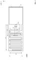
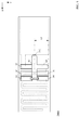
- FIG. 1 is a schematic configuration diagram of a pattern antenna 1000 according to a first embodiment.
- the top view of pattern antenna 1000A which is an example of the pattern antenna of 1st Embodiment.
- the top view of pattern antenna 1000B which is an example of the pattern antenna of 1st Embodiment.
- the figure which shows the frequency-standing wave ratio characteristic of pattern antenna 1000B, and the Smith chart figure of the input impedance of pattern antenna 1000A The schematic block diagram of the pattern antenna 2000 which concerns on 2nd Embodiment.
- FIG. The figure which extracted short circuit part 3C and projection part 3D in pattern antenna 2000, and showed signal waves w1-w5 of an unnecessary frequency typically.
- FIG. The figure which shows an example of the conventional F-shaped pattern antenna 900.
- FIG. The figure which shows pattern antenna 900A (an example).
- FIG. 1 is a schematic configuration diagram of a pattern antenna 1000 according to the first embodiment.
- FIG. 1 shows a plan view (upper view) of the pattern antenna 1000 of the first embodiment, an AA cross-sectional view (middle view), and a bottom view (lower view) of the pattern antenna 1000.
- the X axis and the Y axis are set.
- the pattern antenna 1000 includes a substrate B, a ground portion (GND portion) 1 patterned on the first surface of the substrate B, and a meander-shaped antenna element portion connected to the ground portion 1. 2 is provided. Moreover, the pattern antenna 1000 is provided with the short circuit part 3 on the 2nd surface which is a back surface of a 1st surface, as shown in FIG.
- the substrate B is, for example, a printed circuit board (for example, a glass epoxy substrate), and a pattern is formed by a conductor (for example, copper foil) on the first surface and the second surface (a surface different from the first surface). Can do.
- the substrate B is made of, for example, a material (for example, glass epoxy resin) having a relative dielectric constant of about 4.3.
- FIG. 1 shows the case where the first surface is the surface of the substrate B and the second surface is the surface (back surface) opposite to the first surface, the present invention is not limited to this.
- the substrate B may be a multilayer substrate, and the first surface may be formed on one layer of the substrate B, and the second surface may be formed on another layer. In the following, for convenience of explanation, the case of FIG. 1 (the case where the first surface is the front surface of the substrate B and the second surface is the front surface (back surface) opposite to the first surface) will be described.
- the ground part 1 is a pattern formed on the first surface of the substrate B and is connected to the GND potential.
- the antenna element portion 2 is a meandering pattern (a pattern in which bent portions are repeatedly formed) formed on the first surface of the substrate B. As shown in FIG. 1, the antenna element portion 2 is a pattern formed so as to extend in the positive direction of the X axis while repeatedly forming a bent portion from the end portion of the ground portion 1.
- the pattern of the antenna element portion 2 is formed of a conductor (for example, copper foil).
- the antenna element portion 2 is formed with a through hole (via hole) V1 for electrical connection with the second surface on the pattern of the antenna element portion 2.
- the through hole V1 has a first end in the Y-axis direction of the meander-shaped pattern of the antenna element portion 2 (the end portion indicated by Y coordinate “y0” in FIG. 1) and a second end (Y in FIG. 1). It is preferably provided in the vicinity of an intersection where a line parallel to the X axis and the pattern of the antenna element portion 2 passes through a midpoint with respect to the end portion indicated by the coordinates “y1”.
- the short-circuit portion 3 is formed on the second surface of the substrate B, and is a pattern extending in the X-axis negative direction (direction toward the ground portion 1) from the position including the through hole V1 on the second surface.
- the pattern of the short circuit part 3 is formed of a conductor (for example, copper foil).
- the short circuit part 3 is electrically connected to the antenna element part 2 on the first surface by filling the through hole V1 with a conductor such as solder.
- an antenna transmission / reception unit (for example, an antenna transmission / reception circuit) is installed between the vicinity of the end of the short-circuit unit 3 on the ground unit 1 side and the ground unit 1 in plan view.
- a transmission unit for example, an antenna transmission circuit
- a receiving unit for example, an antenna receiving circuit
- the feeding point 31 is an example and is not limited to the above.
- another portion of the end portion of the short-circuit portion 3 on the ground portion 1 side may be used as a feeding point.
- the feeding point is not limited to a point, and may be a linear region or a planar region (for example, a part or all of the side surface of the end point of the short-circuit portion 3 on the ground portion 1 side).
- the short-circuit portion 3 is formed on the second surface different from the first surface on which the pattern of the antenna element portion 2 is formed.
- the length can be increased. For example, compared to the length d9 of the short-circuit portion 931A when the antenna element portion 93A and the short-circuit portion 931A are formed only on the first surface shown in FIG. 11, in the pattern antenna 1000, as shown in FIG.
- the length d1 of the short-circuit portion 3 can be considerably increased.
- the antenna characteristics can be improved in the pattern antenna 1000. That is, in the pattern antenna 1000, the antenna element portion 2 on the first surface and the short-circuit portion 3 on the second surface are arranged with the substrate B (for example, a substrate having a relative dielectric constant of about 4.3) interposed therebetween. In plan view, part of the antenna element part 2 on the first surface and part of the short-circuit part 3 on the second surface overlap, so that capacitive coupling can be generated. Specifically, in the areas AR1, AR2, and AR3 in the AA cross-sectional view (middle diagram) of FIG. 1, the conductor pattern of the antenna element portion 2 and the conductor pattern of the short-circuit portion 3 sandwich the substrate B.
- the substrate B for example, a substrate having a relative dielectric constant of about 4.3
- the pattern antenna 1000 since the short-circuit portion 3 is formed on the second surface different from the first surface, the area necessary for forming the short-circuit portion can be reduced, and as a result, desired The pattern antenna 1000 that realizes the antenna characteristics can be configured in a small area.
- the capacitive coupling can be generated by forming the short-circuit portion 3. Therefore, conventionally, in order to realize a desired antenna characteristic, or impedance It is possible to eliminate the LC circuit or the like necessary for the adjustment or to reduce the circuit scale. That is, with the pattern antenna 1000, desired antenna characteristics can be realized, impedance adjustment can be performed appropriately, and the circuit scale of the antenna circuit connected to the pattern antenna 1000 can be reduced.
- impedance adjustment target impedance is set to 50 [ ⁇ ] in the pattern antenna 1000 of the first embodiment will be described below.
- FIG. 2 is a plan view of a pattern antenna 1000A that is an example of the pattern antenna according to the first embodiment (similar to the upper diagram in FIG. 1).
- the length L1 in the longitudinal direction of the antenna element portion 2 (the length indicated by L1 in FIG. 2) is 33.4 [mm]
- the width W1 of the antenna element portion 2 (FIG. 2 is 15.8 [mm]
- the length L2 in the longitudinal direction of the short-circuit portion 3 is 14.7 [mm].
- the width W2 of the short-circuit portion 3A (the length indicated by W2 in FIG. 2) is 1.85 [mm].
- FIG. 3 is a plan view of a pattern antenna 1000B which is an example of the pattern antenna of the first embodiment (similar to the upper diagram of FIG. 1).
- the length L1 in the longitudinal direction of the antenna element portion 2 (the length indicated by L1 in FIG. 2) is the same as in FIG. 2, and is 33.4 [mm].
- the width W1 (the length indicated by W1 in FIG. 2) of the element portion 2 is the same as that in FIG. 2 and is 15.8 [mm].
- the length L2 in the longitudinal direction of the short-circuit portion 3 (the length indicated by L2 in FIG. 2) is the same as in FIG. 2 and is 14.7 [mm], and the width W2 of the short-circuit portion 3B (in FIG.
- the short-circuit portion 3B of the pattern antenna 1000B has a circular arc shape at the end on the ground portion 1 side in a plan view, but the short-circuit portion 3B is not limited to this, It may be rectangular in plan view.
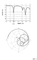
- FIG. 4 shows a frequency-standing wave ratio characteristic of the pattern antenna 1000A (upper diagram) and a Smith chart of the input impedance of the pattern antenna 1000A (lower diagram).
- FIG. 5 shows a frequency-standing wave ratio characteristic of the pattern antenna 1000B (upper diagram) and a Smith chart of the input impedance of the pattern antenna 1000A (lower diagram).
- the frequency of the use signal (the signal (electromagnetic wave) to be transmitted / received by the pattern antenna) is 925 [MHz].
- the pattern antenna 1000A has a 925 [MHz] and a standing wave ratio of -12.4 [dB].
- Z 64.9 + j ⁇ 24.1 at 925 [MHz]
- the pattern antenna 1000B has a standing wave ratio of 925 [MHz] and a standing wave ratio of ⁇ 15.7 [dB].
- an impedance matching circuit is provided between the feeding point 31B of the short-circuit portion 3B and the ground portion 1.
- the width W2 of the short-circuit portion 3B of the pattern antenna 1000B is thicker than the width of the short-circuit portion 3A of the pattern antenna 1000A. Therefore, in the plan view, in the pattern antenna 1000B, the area where the pattern of the antenna element portion 2 and the short-circuit portion 3B overlap (for example, the area of TB1 and TB2 shown in FIG. 3) is the pattern of the antenna element portion 2 of the pattern antenna 1000A. And the area where the short-circuit portion 3A overlaps (for example, the areas of TA1 and TA2 shown in FIG. 2).
- the pattern antenna 1000B has a standing wave ratio at 925 [MHz] of -15.7 [dB]
- the pattern antenna 1000A has a standing wave ratio at 925 [MHz]. This is an improvement of 3.3 [dB] over ( ⁇ 12.4 [dB]).
- the pattern antenna of the present invention it is possible to easily adjust the frequency characteristics and input impedance characteristics of the antenna so as to approach the desired characteristics only by adjusting the width of the short-circuit portion of the pattern antenna.
- the pattern antenna of the present invention As a result, with the pattern antenna of the present invention, desired antenna characteristics can be realized, impedance adjustment can be performed appropriately, and the circuit scale of the antenna circuit connected to the pattern antenna can be reduced. it can.
- the relative dielectric constant between the first surface (the surface on which the ground portion 1 and the antenna element portion 2 are formed) and the second surface (the surface on which the short-circuit portion 3 is formed) is predetermined. And adjust the input impedance of the pattern antenna 1000 by adjusting the positional relationship and shape of the antenna element portion 2 and the short-circuit portion 3 in plan view as described above. Also good.
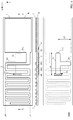
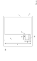
- FIG. 6 is a schematic configuration diagram of a pattern antenna 2000 according to the second embodiment.
- FIG. 6 shows a plan view (upper view) of the pattern antenna 2000 according to the second embodiment, an AA sectional view (middle view), and a bottom view (lower view) of the pattern antenna 2000. Also, as shown in FIG. 6, the X axis and the Y axis are set.
- the pattern antenna 2000 includes a substrate B, a ground portion (GND portion) 1 patterned on the first surface of the substrate B, and a meander-shaped antenna element portion connected to the ground portion 1. 2 is provided. Further, as shown in FIG. 6, the pattern antenna 2000 includes a short-circuit portion 3C and a protrusion 3D extending from the short-circuit portion 3C in the Y-axis direction on the second surface, which is the back surface of the first surface.
- the protrusion 3D is formed to have a length L3 in the Y-axis direction from a substantially center position in the width direction (Y-axis direction) of the short-circuit portion 3C.
- the length L3 may be set to a length substantially equal to ⁇ / 4, where ⁇ is the wavelength of the frequency component of a signal to be excluded (a signal that is not desired to be transmitted / received by the pattern antenna).
- the protrusion 3D is formed so as to overlap the pattern of the antenna element 2 in a plan view.
- the portion where the pattern of the short-circuit portion 3C and the pattern of the antenna element portion 2 overlap is equivalent to a capacitor installed in parallel with the feeding point 31C of the short-circuit portion 3C and the ground portion 1.
- Capacitance (capacitance component) can be added to the input impedance of the antenna 2000.
- length L3 of the protrusion 3D shown in FIG. 6 may be determined as follows.
- L3A ⁇ 0 / 4 ⁇ 0.3 ⁇ ( ⁇ 0 / 4) sqrt (x): You may make it equal to length L3A which satisfy
- the capacitance contribution ratio Kc is (1) the conductor pattern of the antenna element portion 2 and the conductor of the protrusion portion 3D in a portion where the conductor pattern of the antenna element portion 2 and the conductor pattern of the protrusion portion 3D overlap in plan view.
- the capacitance contribution rate Kc can be determined. Therefore, as described above, the shape (for example, the length L3) of the protrusion is determined based on the determined capacitance contribution rate Kc. can do.
- the length L3 of the protrusion 3D shown in FIG. 6 may be determined.
- An antenna in which the antenna element portion 2 has a complicated shape such as the pattern antenna 1000 shown in the first embodiment and the pattern antenna 2000 of the present embodiment, often has multiband characteristics.
- the standing wave ratio is small at 2.5 [GHz] in addition to the frequency 925 [MHz] of the used signal, and 2.5 [GHz]. It also shows good antenna characteristics for signals (electromagnetic waves). That is, the pattern antenna 1000B has a multiband characteristic that can satisfactorily transmit and receive a signal of frequency 925 [MHz] and a signal of 2.5 [GHz].
- the signal of 2.5 [GHz] is an unnecessary signal, and the antenna characteristics per 2.5 [GHz] are improved (per 2.5 [GHz]. It is necessary to improve the characteristics so that no signal is transmitted or received.
- the pattern antenna 2000 of the present embodiment as shown in FIG. Thereby, when it has multiband characteristics, the input impedance in the vicinity of the frequency of the unnecessary signal is changed, and the antenna transmission / reception sensitivity of the unnecessary signal is lowered.
- the pattern antenna 2000 of the present embodiment has good antenna transmission / reception sensitivity only near the frequency of the used signal, and can transmit / receive only the used signal.
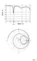
- FIG. 7 shows an antenna characteristic (example) of the pattern antenna 2000 of the present embodiment. Specifically, FIG. 7 shows the frequency-standing wave ratio characteristics (upper figure) of the pattern antenna 2000 with the protrusion 3D added to the pattern antenna 1000B having the antenna characteristics of FIG. The impedance Smith chart (lower figure) is shown.
- the pattern antenna 2000 has a 925 [MHz] and a standing wave ratio of ⁇ 17.9 [dB].
- the input impedance of the pattern antenna 2000 can be brought close to 50 [ ⁇ ].
- the frequency-standing wave ratio characteristic (upper figure) of the pattern antenna 2000 exists in the frequency-standing wave ratio characteristic (upper figure) of the pattern antenna 1000B of FIG.
- the peak around 5 [GHz] has disappeared, and multiband characteristics are not exhibited. That is, in the pattern antenna 2000, by providing the protrusion 3D, the input impedance per 2.5 [GHz] changes, and the characteristics are improved so that the signal per 2.5 [GHz] is not passed. .
- the input impedance is closer to 50 [ ⁇ ] compared to the pattern antenna of the first embodiment, it is connected to the pattern antenna in order to adjust the input impedance to 50 [ ⁇ ].
- the circuit scale of the antenna circuit can be further reduced.
- the principle that the projection antenna 3D can be prevented from receiving the signal of the unnecessary frequency (the antenna transmission / reception sensitivity of the signal of the unnecessary frequency can be lowered) is described with reference to FIG. To do.
- FIG. 8 is a diagram schematically showing signal waves w1 to w5 having unnecessary frequencies by extracting the short-circuit portion 3C and the projection portion 3D in the pattern antenna 2000.
- FIG. 8 is a diagram schematically showing signal waves w1 to w5 having unnecessary frequencies by extracting the short-circuit portion 3C and the projection portion 3D in the pattern antenna 2000.
- the signal wave w1 of the unnecessary frequency that has entered from the antenna element portion 2 side propagates to the protrusion 3D side and the feeding point side at the point A1 shown in FIG.
- the signal wave w2 having an unnecessary frequency that propagates from the point A1 to the protrusion 3D is reflected by the tip of the protrusion 3D. Since the projecting portion 3D is an open stub, the signal wave w2 is totally reflected at the open end, and thus is reflected without changing the phase (with a phase difference of 0) and propagates to the point A1 as a reflected wave w3. .
- the reflected wave w3 that has reached the point A1 is propagated as a signal wave w5 from the point A1 to the antenna element part 2 side and to the feeding point side.
- the signal wave w5 reciprocates the distance from the point A1 to the tip of the protrusion 3D, that is, propagates a distance of 2 ⁇ ⁇ 1 / 4
- the signal wave w5 is the signal wave w1. Is shifted in phase by ⁇ with respect to the signal W4 propagated to the feeding point side as it is. That is, since the signal wave w4 and the signal wave w5 are in opposite phases, the signal components of both are canceled out. As a result, an unnecessary frequency signal is not propagated to the feeding point.
- the unnecessary signal is fed to the pattern antenna 2000 by setting the distance from the center in the width direction of the short-circuit portion 3C to the tip of the protrusion 3D to 1 ⁇ 4 of the wavelength of the unnecessary signal. Propagation to the point side can be prevented.
- the antenna transmission / reception sensitivity of the unnecessary frequency component can be deteriorated, and the antenna characteristics of the pattern antenna 2000 can be improved.
- the antenna sensitivity to the electromagnetic waves to be excluded may be reduced in consideration of the wavelength shortening effect.
- the wavelength shortening effect means that when a high-frequency signal (high-frequency electromagnetic wave) passes through the conductor, the high-frequency signal passes through the conductor due to the influence of the relative permittivity of the material around the conductor. This means the effect of shortening the wavelength of the high-frequency signal.
- the position of the protrusion 3D of the pattern antenna 2000 may be other than the position described above.
- a protrusion may be formed to extend from the short-circuit portion 3C at any position 3F to 3I shown in FIG.
- the protrusions may be formed at any two or more positions indicated by 3D to 3I in FIG.
- a protrusion may be formed so as to extend from the short-circuit portion 3C in an arbitrary direction (for example, an oblique direction).
- the signal from the point on the center line in the width direction (Y-axis direction) of the short-circuit portion 3C to the tip of the protruding portion extending in an arbitrary direction is not desired to be transmitted / received by an antenna, for example.
- the wavelength By setting the wavelength to about 1/4 of the signal to be removed, the signal component (the signal component of the unnecessary signal) can be efficiently removed.
- the protruding portion 3D extending from the short-circuit portion 3C can efficiently remove unnecessary signals, improve the antenna characteristics, and provide capacitance (capacitance component).
- the input impedance is also close to the desired value.
- the first surface of the substrate B (the surface on which the ground portion 1 and the antenna element portion 2 are formed) and the second surface (the surface on which the short-circuit portion 3C and the protruding portions 3D (3E to 3I) are formed).
- the relative dielectric constant between the antenna element portion 2 and the short-circuit portion 3 in the plan view is adjusted as described above, and the positional relationship and shape of the antenna element portion 2 and the short-circuit portion 3 are adjusted as described above.
- the input impedance may be adjusted.
Landscapes
- Details Of Aerials (AREA)
- Waveguide Aerials (AREA)
Priority Applications (1)
| Application Number | Priority Date | Filing Date | Title |
|---|---|---|---|
| US14/983,662 US9780454B2 (en) | 2013-08-08 | 2015-12-30 | Pattern antenna |
Applications Claiming Priority (2)
| Application Number | Priority Date | Filing Date | Title |
|---|---|---|---|
| JP2013164803A JP6163381B2 (ja) | 2013-08-08 | 2013-08-08 | パターンアンテナ |
| JP2013-164803 | 2013-08-08 |
Related Child Applications (1)
| Application Number | Title | Priority Date | Filing Date |
|---|---|---|---|
| US14/983,662 Continuation US9780454B2 (en) | 2013-08-08 | 2015-12-30 | Pattern antenna |
Publications (1)
| Publication Number | Publication Date |
|---|---|
| WO2015019799A1 true WO2015019799A1 (ja) | 2015-02-12 |
Family
ID=52461138
Family Applications (1)
| Application Number | Title | Priority Date | Filing Date |
|---|---|---|---|
| PCT/JP2014/068677 Ceased WO2015019799A1 (ja) | 2013-08-08 | 2014-07-14 | パターンアンテナ |
Country Status (3)
| Country | Link |
|---|---|
| US (1) | US9780454B2 (enExample) |
| JP (1) | JP6163381B2 (enExample) |
| WO (1) | WO2015019799A1 (enExample) |
Cited By (1)
| Publication number | Priority date | Publication date | Assignee | Title |
|---|---|---|---|---|
| US9905915B2 (en) | 2015-08-26 | 2018-02-27 | Megachips Corporation | Pattern antenna |
Families Citing this family (4)
| Publication number | Priority date | Publication date | Assignee | Title |
|---|---|---|---|---|
| FR3030771B1 (fr) * | 2014-12-22 | 2017-01-27 | Thales Sa | Procede de mesure d'une direction d'incidence d'une onde incidente pour un recepteur a large bande instantanee et recepteur associe |
| USD776093S1 (en) * | 2015-04-08 | 2017-01-10 | Avery Dennison Retail Information Services, Llc | Antenna |
| USD858492S1 (en) * | 2017-08-22 | 2019-09-03 | Megabyte Limited | RFID tag inlay |
| USD874447S1 (en) * | 2018-11-14 | 2020-02-04 | Avery Dennison Retail Information Services Llc | Antenna |
Citations (5)
| Publication number | Priority date | Publication date | Assignee | Title |
|---|---|---|---|---|
| JP2004242297A (ja) * | 2003-01-16 | 2004-08-26 | Matsushita Electric Ind Co Ltd | アンテナ |
| JP2005110109A (ja) * | 2003-10-01 | 2005-04-21 | Auto Network Gijutsu Kenkyusho:Kk | パターンアンテナ |
| JP2005136784A (ja) * | 2003-10-31 | 2005-05-26 | Nissei Electric Co Ltd | 平面アンテナ |
| JP2012209752A (ja) * | 2011-03-29 | 2012-10-25 | Fujitsu Component Ltd | アンテナ装置、回路基板及びメモリカード |
| JP2013517727A (ja) * | 2010-01-20 | 2013-05-16 | インサイト・シップ・エスーアーエス | パッケージ内の改良されたアンテナ構造 |
Family Cites Families (6)
| Publication number | Priority date | Publication date | Assignee | Title |
|---|---|---|---|---|
| US6166694A (en) * | 1998-07-09 | 2000-12-26 | Telefonaktiebolaget Lm Ericsson (Publ) | Printed twin spiral dual band antenna |
| US6664931B1 (en) * | 2002-07-23 | 2003-12-16 | Motorola, Inc. | Multi-frequency slot antenna apparatus |
| CN100379084C (zh) | 2003-01-16 | 2008-04-02 | 松下电器产业株式会社 | 天线 |
| DE10319093B3 (de) * | 2003-04-28 | 2004-11-04 | Fraunhofer-Gesellschaft zur Förderung der angewandten Forschung e.V. | Antennenvorrichtung |
| US6809689B1 (en) * | 2003-05-20 | 2004-10-26 | Quanta Computer Inc. | Multi-frequency antenna for a portable electronic apparatus |
| JP2009194783A (ja) | 2008-02-18 | 2009-08-27 | Nec Engineering Ltd | パターンアンテナ及びパターンアンテナを親基板に実装したアンテナ装置 |
-
2013
- 2013-08-08 JP JP2013164803A patent/JP6163381B2/ja not_active Expired - Fee Related
-
2014
- 2014-07-14 WO PCT/JP2014/068677 patent/WO2015019799A1/ja not_active Ceased
-
2015
- 2015-12-30 US US14/983,662 patent/US9780454B2/en active Active
Patent Citations (5)
| Publication number | Priority date | Publication date | Assignee | Title |
|---|---|---|---|---|
| JP2004242297A (ja) * | 2003-01-16 | 2004-08-26 | Matsushita Electric Ind Co Ltd | アンテナ |
| JP2005110109A (ja) * | 2003-10-01 | 2005-04-21 | Auto Network Gijutsu Kenkyusho:Kk | パターンアンテナ |
| JP2005136784A (ja) * | 2003-10-31 | 2005-05-26 | Nissei Electric Co Ltd | 平面アンテナ |
| JP2013517727A (ja) * | 2010-01-20 | 2013-05-16 | インサイト・シップ・エスーアーエス | パッケージ内の改良されたアンテナ構造 |
| JP2012209752A (ja) * | 2011-03-29 | 2012-10-25 | Fujitsu Component Ltd | アンテナ装置、回路基板及びメモリカード |
Cited By (2)
| Publication number | Priority date | Publication date | Assignee | Title |
|---|---|---|---|---|
| US9905915B2 (en) | 2015-08-26 | 2018-02-27 | Megachips Corporation | Pattern antenna |
| US10141637B2 (en) | 2015-08-26 | 2018-11-27 | Megachips Corporation | Pattern antenna |
Also Published As
| Publication number | Publication date |
|---|---|
| JP6163381B2 (ja) | 2017-07-12 |
| US20160111791A1 (en) | 2016-04-21 |
| JP2015035679A (ja) | 2015-02-19 |
| US9780454B2 (en) | 2017-10-03 |
Similar Documents
| Publication | Publication Date | Title |
|---|---|---|
| CN104112909B (zh) | 分集天线组合及其可动态调整输入阻抗的宽频天线 | |
| USRE47068E1 (en) | Microstrip antenna and radar module | |
| US9905915B2 (en) | Pattern antenna | |
| JP6163381B2 (ja) | パターンアンテナ | |
| CN106299671A (zh) | 双频带滤波天线 | |
| US9746555B2 (en) | Planar antenna and radar apparatus | |
| CN101986461A (zh) | 整合式多频天线 | |
| WO2011021677A1 (ja) | アンテナモジュール | |
| CN103872430A (zh) | 电子设备、天线、和用于形成天线的方法 | |
| CN107026313B (zh) | 用于无线通信模块的天线 | |
| JP5863730B2 (ja) | アンテナ装置及び無線通信装置 | |
| JP6351450B2 (ja) | 無線モジュール、電子モジュール及び測定方法 | |
| JP2015035679A5 (enExample) | ||
| TWI508379B (zh) | 單極天線 | |
| JP2009194783A (ja) | パターンアンテナ及びパターンアンテナを親基板に実装したアンテナ装置 | |
| TWI354401B (en) | Dual-band antenna | |
| CN106505306B (zh) | 一种移动设备的天线及应用该天线的移动设备 | |
| CN111373603B (zh) | 通信设备 | |
| JP6548112B2 (ja) | 広帯域アンテナ | |
| EP3665740B1 (en) | Waveguide antenna magnetoelectric matching transition | |
| CN216354787U (zh) | 天线装置及智能电视 | |
| TWI783791B (zh) | 天線模組 | |
| US11310908B2 (en) | Circuit board, inductor, and radio apparatus | |
| CN102347525A (zh) | 微型积层天线 | |
| CN104078755B (zh) | 单极天线 |
Legal Events
| Date | Code | Title | Description |
|---|---|---|---|
| 121 | Ep: the epo has been informed by wipo that ep was designated in this application |
Ref document number: 14833815 Country of ref document: EP Kind code of ref document: A1 |
|
| NENP | Non-entry into the national phase |
Ref country code: DE |
|
| 122 | Ep: pct application non-entry in european phase |
Ref document number: 14833815 Country of ref document: EP Kind code of ref document: A1 |