WO2015019799A1 - パターンアンテナ - Google Patents
パターンアンテナ Download PDFInfo
- Publication number
- WO2015019799A1 WO2015019799A1 PCT/JP2014/068677 JP2014068677W WO2015019799A1 WO 2015019799 A1 WO2015019799 A1 WO 2015019799A1 JP 2014068677 W JP2014068677 W JP 2014068677W WO 2015019799 A1 WO2015019799 A1 WO 2015019799A1
- Authority
- WO
- WIPO (PCT)
- Prior art keywords
- antenna
- pattern
- short
- substrate
- conductor pattern
- Prior art date
Links
- 239000004020 conductor Substances 0.000 claims abstract description 66
- 239000000758 substrate Substances 0.000 claims abstract description 50
- 230000035945 sensitivity Effects 0.000 description 15
- 238000010586 diagram Methods 0.000 description 14
- 230000005540 biological transmission Effects 0.000 description 10
- 230000000694 effects Effects 0.000 description 9
- 238000004904 shortening Methods 0.000 description 9
- 239000000463 material Substances 0.000 description 5
- 230000000644 propagated effect Effects 0.000 description 5
- 230000008878 coupling Effects 0.000 description 4
- 238000010168 coupling process Methods 0.000 description 4
- 238000005859 coupling reaction Methods 0.000 description 4
- RYGMFSIKBFXOCR-UHFFFAOYSA-N Copper Chemical compound [Cu] RYGMFSIKBFXOCR-UHFFFAOYSA-N 0.000 description 3
- 239000011889 copper foil Substances 0.000 description 3
- 239000003990 capacitor Substances 0.000 description 2
- 239000011521 glass Substances 0.000 description 2
- 239000004593 Epoxy Substances 0.000 description 1
- 238000005452 bending Methods 0.000 description 1
- 238000005516 engineering process Methods 0.000 description 1
- 239000003822 epoxy resin Substances 0.000 description 1
- 239000004615 ingredient Substances 0.000 description 1
- 238000000034 method Methods 0.000 description 1
- 238000012986 modification Methods 0.000 description 1
- 230000004048 modification Effects 0.000 description 1
- 238000000059 patterning Methods 0.000 description 1
- 229920000647 polyepoxide Polymers 0.000 description 1
- 230000001902 propagating effect Effects 0.000 description 1
- 229910000679 solder Inorganic materials 0.000 description 1
- 239000000126 substance Substances 0.000 description 1
Images


Classifications
-
- H—ELECTRICITY
- H01—ELECTRIC ELEMENTS
- H01Q—ANTENNAS, i.e. RADIO AERIALS
- H01Q9/00—Electrically-short antennas having dimensions not more than twice the operating wavelength and consisting of conductive active radiating elements
- H01Q9/04—Resonant antennas
- H01Q9/0407—Substantially flat resonant element parallel to ground plane, e.g. patch antenna
- H01Q9/0414—Substantially flat resonant element parallel to ground plane, e.g. patch antenna in a stacked or folded configuration
-
- H—ELECTRICITY
- H01—ELECTRIC ELEMENTS
- H01Q—ANTENNAS, i.e. RADIO AERIALS
- H01Q1/00—Details of, or arrangements associated with, antennas
- H01Q1/36—Structural form of radiating elements, e.g. cone, spiral, umbrella; Particular materials used therewith
-
- H—ELECTRICITY
- H01—ELECTRIC ELEMENTS
- H01Q—ANTENNAS, i.e. RADIO AERIALS
- H01Q1/00—Details of, or arrangements associated with, antennas
- H01Q1/36—Structural form of radiating elements, e.g. cone, spiral, umbrella; Particular materials used therewith
- H01Q1/38—Structural form of radiating elements, e.g. cone, spiral, umbrella; Particular materials used therewith formed by a conductive layer on an insulating support
-
- H—ELECTRICITY
- H01—ELECTRIC ELEMENTS
- H01Q—ANTENNAS, i.e. RADIO AERIALS
- H01Q9/00—Electrically-short antennas having dimensions not more than twice the operating wavelength and consisting of conductive active radiating elements
- H01Q9/04—Resonant antennas
- H01Q9/30—Resonant antennas with feed to end of elongated active element, e.g. unipole
- H01Q9/42—Resonant antennas with feed to end of elongated active element, e.g. unipole with folded element, the folded parts being spaced apart a small fraction of the operating wavelength
Definitions
- the present invention relates to a pattern antenna and an antenna device including the pattern antenna.
- F-shaped pattern antennas have been widely used as antennas for mounting on small devices.
- the F-shaped pattern antenna is configured by patterning antenna elements on the surface of a printed circuit board so as to be F-shaped.
- a high frequency antenna can be formed in a relatively small area on the printed circuit board.
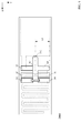
- FIG. 10 is a diagram illustrating an example of a conventional F-shaped pattern antenna 900.
- the F-shaped pattern antenna 900 includes a substrate 91, a ground surface 92 patterned on the substrate 91, and an antenna element 93 connected to the ground surface 92. Further, the F-shaped pattern antenna 900 includes feed points 94 and 95 as shown in FIG.
- the length L91 of the antenna element 93 in FIG. 10 is set to about ⁇ / 4, so that good antenna characteristics (frequency characteristics) can be obtained.
- the distance from the feed point 94 to the GND plane the distance indicated by the arrow M1 in FIG. 10
- the position of the feed point 94 By adjusting (the length indicated by L92 in FIG. 10), the capacitance component and the inductance component are adjusted, and the input impedance can be brought close to 50 ⁇ .
- the antenna element 93 has a configuration extending in the vertical direction of FIG. 10, and the length L91 needs to be about ⁇ / 4. It is difficult to configure a pattern antenna in a small area region while maintaining the antenna performance of the F-shaped pattern antenna 900.
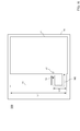
- the pattern antenna 900A shown in FIG. 11 by bending the antenna element portion (by forming the antenna element portion in a meander shape), a region having a smaller area while ensuring the length of the antenna element portion. It is conceivable to form a pattern antenna.
- the area required for the short-circuit portion 931A extending from the meander-shaped portion closest to the GND surface 92A of the antenna element portion 93A toward the feeding point 94A is narrowed. That is, as shown in FIG. 11, since the range in which the position of the short-circuit portion 931A can be adjusted is limited, in the pattern antenna 900A, the position of the short-circuit portion 931A can be adjusted to obtain desired antenna characteristics, It becomes difficult to achieve matching.
- an object of the present invention is to realize a pattern antenna having desired antenna characteristics and capable of being formed even in a small area.
- a first invention is a pattern antenna including a substrate, a ground portion formed on the first surface of the substrate, an antenna element portion, a short-circuit portion, and a connection portion.
- the antenna element portion includes a conductor pattern provided so that a plurality of bent portions are formed on the first surface of the substrate, and is electrically connected to the ground portion.
- the short-circuit portion overlaps at least a part of the conductor pattern of the antenna element portion in plan view with the conductor pattern of the antenna element portion of the first surface and the second surface that is different from the first surface of the substrate. Including a provided conductor pattern.
- connection part electrically connects the conductor pattern of the antenna element part and the conductor pattern of the short-circuit part.
- the conductor pattern of the antenna element portion is provided so that a plurality of bent portions are formed on the first surface of the substrate, so that the length of the necessary conductor pattern of the antenna is ensured and small.
- An antenna element portion can be provided in the area region.
- the short-circuit portion is electrically connected to the antenna element portion on the first surface of the substrate and is formed on the second surface of the substrate.
- a short-circuit portion having a size (length) can be formed.
- the capacitance (capacitance component) can be imparted to the input impedance by adjusting the overlapping state of the conductor pattern of the short circuit portion and the conductor pattern of the antenna element portion in plan view.
- this pattern antenna it is easy to realize desired antenna characteristics and to easily adjust the input impedance. As a result, the circuit scale of the transmission / reception circuit required for impedance adjustment can be reduced. That is, with this pattern antenna, the area required to form the pattern antenna can be reduced, and desired antenna characteristics can be easily realized.
- the substrate may be a multilayer substrate, and the first surface may be formed on one layer of the substrate, and the second surface may be formed on another layer.
- 2nd invention is 1st invention, Comprising: An antenna element part contains the conductor pattern formed in meander shape.
- the antenna element portion can be configured in a small area.
- 3rd invention is 1st or 2nd invention, Comprising: It electrically connects to a short circuit part in the 2nd surface of a board
- the antenna sensitivity to unnecessary signals can be reduced. That is, when the antenna element portion has a complicated shape, it may have multiband characteristics. Even in such a case, in this pattern antenna, the antenna sensitivity to an unnecessary signal (electromagnetic wave) can be reduced by providing a protrusion and adjusting the shape and position of the protrusion. As a result, this pattern antenna can appropriately prevent the multiband characteristic.
- desired capacitance (capacitance component) can be imparted by adjusting the degree of overlap between the conductor pattern of the projecting portion and the conductor pattern of the antenna element portion in plan view. Therefore, with this pattern antenna, desired antenna characteristics can be easily realized.
- 4th invention is 3rd invention, Comprising: A short circuit part and a projection part are rectangular shapes.
- the electromagnetic wave of wavelength ⁇ (electromagnetic wave to be excluded) that has been totally reflected from the short-circuited portion at the tip of the protruding portion and the feeding point (for connecting the antenna transmitting / receiving unit) from the short-circuited portion
- the phase difference from the electromagnetic wave having the wavelength ⁇ (the electromagnetic wave to be excluded) propagating to the connection point on the short-circuit portion is about ⁇ , and the phase is reversed. That is, the electromagnetic wave having the wavelength ⁇ that is directly propagated to the feeding point cancels out the electromagnetic wave having the wavelength ⁇ that is totally reflected by the protrusion and propagated to the feeding point.
- this pattern antenna it is possible to reduce the antenna sensitivity with respect to the electromagnetic waves to be excluded.
- 5th invention is 3rd invention, Comprising: A short circuit part and a projection part are rectangular shape.
- the antenna sensitivity to the electromagnetic waves to be excluded can be reduced in consideration of the wavelength shortening effect.
- the wavelength shortening effect means that when a high-frequency signal (high-frequency electromagnetic wave) passes through the conductor, the high-frequency signal passes through the conductor due to the influence of the relative permittivity of the material around the conductor. This means the effect of shortening the wavelength of the high-frequency signal.
- 6th invention is 3rd invention, Comprising: A short circuit part and a projection part are rectangular shapes.
- the wavelength shortening effect is taken into consideration, and the capacitance contribution ratio generated by overlapping the conductor pattern of the antenna element portion and the conductor pattern of the protrusion portion in a plan view is expressed as Kc (0 ⁇ Kc ⁇ 1). ) Can be taken into consideration, and the antenna sensitivity to the electromagnetic waves to be excluded can be reduced.
- a capacitance component (capacitance component) is added to the input impedance of the pattern antenna by overlapping the conductor pattern of the antenna element portion and the conductor pattern of the projection portion. ),
- the length L2 is determined by the above formula using the capacitance contribution ratio Kc in consideration of the influence of the above), thereby reducing the antenna sensitivity to the electromagnetic waves to be excluded and further reducing the size of the protrusions. it can.
- this pattern antenna can be configured with a smaller area, and the antenna sensitivity to electromagnetic waves to be excluded can be appropriately reduced.
- the seventh invention is any one of the third to sixth inventions, wherein a plurality of protrusions are formed on the second surface of the substrate so as not to overlap each other.
- this pattern antenna the antenna sensitivity to, for example, a plurality of electromagnetic waves having unnecessary frequencies can be reduced by the plurality of protrusions.
- desired capacitance capacitance component
- desired antenna characteristics can be easily realized.
- An object of the present invention is to realize a pattern antenna that has desired antenna characteristics and can be formed in a small area.
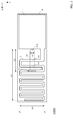
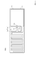
- FIG. 1 is a schematic configuration diagram of a pattern antenna 1000 according to a first embodiment.
- the top view of pattern antenna 1000A which is an example of the pattern antenna of 1st Embodiment.
- the top view of pattern antenna 1000B which is an example of the pattern antenna of 1st Embodiment.
- the figure which shows the frequency-standing wave ratio characteristic of pattern antenna 1000B, and the Smith chart figure of the input impedance of pattern antenna 1000A The schematic block diagram of the pattern antenna 2000 which concerns on 2nd Embodiment.
- FIG. The figure which extracted short circuit part 3C and projection part 3D in pattern antenna 2000, and showed signal waves w1-w5 of an unnecessary frequency typically.
- FIG. The figure which shows an example of the conventional F-shaped pattern antenna 900.
- FIG. The figure which shows pattern antenna 900A (an example).
- FIG. 1 is a schematic configuration diagram of a pattern antenna 1000 according to the first embodiment.
- FIG. 1 shows a plan view (upper view) of the pattern antenna 1000 of the first embodiment, an AA cross-sectional view (middle view), and a bottom view (lower view) of the pattern antenna 1000.
- the X axis and the Y axis are set.
- the pattern antenna 1000 includes a substrate B, a ground portion (GND portion) 1 patterned on the first surface of the substrate B, and a meander-shaped antenna element portion connected to the ground portion 1. 2 is provided. Moreover, the pattern antenna 1000 is provided with the short circuit part 3 on the 2nd surface which is a back surface of a 1st surface, as shown in FIG.
- the substrate B is, for example, a printed circuit board (for example, a glass epoxy substrate), and a pattern is formed by a conductor (for example, copper foil) on the first surface and the second surface (a surface different from the first surface). Can do.
- the substrate B is made of, for example, a material (for example, glass epoxy resin) having a relative dielectric constant of about 4.3.
- FIG. 1 shows the case where the first surface is the surface of the substrate B and the second surface is the surface (back surface) opposite to the first surface, the present invention is not limited to this.
- the substrate B may be a multilayer substrate, and the first surface may be formed on one layer of the substrate B, and the second surface may be formed on another layer. In the following, for convenience of explanation, the case of FIG. 1 (the case where the first surface is the front surface of the substrate B and the second surface is the front surface (back surface) opposite to the first surface) will be described.
- the ground part 1 is a pattern formed on the first surface of the substrate B and is connected to the GND potential.
- the antenna element portion 2 is a meandering pattern (a pattern in which bent portions are repeatedly formed) formed on the first surface of the substrate B. As shown in FIG. 1, the antenna element portion 2 is a pattern formed so as to extend in the positive direction of the X axis while repeatedly forming a bent portion from the end portion of the ground portion 1.
- the pattern of the antenna element portion 2 is formed of a conductor (for example, copper foil).
- the antenna element portion 2 is formed with a through hole (via hole) V1 for electrical connection with the second surface on the pattern of the antenna element portion 2.
- the through hole V1 has a first end in the Y-axis direction of the meander-shaped pattern of the antenna element portion 2 (the end portion indicated by Y coordinate “y0” in FIG. 1) and a second end (Y in FIG. 1). It is preferably provided in the vicinity of an intersection where a line parallel to the X axis and the pattern of the antenna element portion 2 passes through a midpoint with respect to the end portion indicated by the coordinates “y1”.
- the short-circuit portion 3 is formed on the second surface of the substrate B, and is a pattern extending in the X-axis negative direction (direction toward the ground portion 1) from the position including the through hole V1 on the second surface.
- the pattern of the short circuit part 3 is formed of a conductor (for example, copper foil).
- the short circuit part 3 is electrically connected to the antenna element part 2 on the first surface by filling the through hole V1 with a conductor such as solder.
- an antenna transmission / reception unit (for example, an antenna transmission / reception circuit) is installed between the vicinity of the end of the short-circuit unit 3 on the ground unit 1 side and the ground unit 1 in plan view.
- a transmission unit for example, an antenna transmission circuit
- a receiving unit for example, an antenna receiving circuit
- the feeding point 31 is an example and is not limited to the above.
- another portion of the end portion of the short-circuit portion 3 on the ground portion 1 side may be used as a feeding point.
- the feeding point is not limited to a point, and may be a linear region or a planar region (for example, a part or all of the side surface of the end point of the short-circuit portion 3 on the ground portion 1 side).
- the short-circuit portion 3 is formed on the second surface different from the first surface on which the pattern of the antenna element portion 2 is formed.
- the length can be increased. For example, compared to the length d9 of the short-circuit portion 931A when the antenna element portion 93A and the short-circuit portion 931A are formed only on the first surface shown in FIG. 11, in the pattern antenna 1000, as shown in FIG.
- the length d1 of the short-circuit portion 3 can be considerably increased.
- the antenna characteristics can be improved in the pattern antenna 1000. That is, in the pattern antenna 1000, the antenna element portion 2 on the first surface and the short-circuit portion 3 on the second surface are arranged with the substrate B (for example, a substrate having a relative dielectric constant of about 4.3) interposed therebetween. In plan view, part of the antenna element part 2 on the first surface and part of the short-circuit part 3 on the second surface overlap, so that capacitive coupling can be generated. Specifically, in the areas AR1, AR2, and AR3 in the AA cross-sectional view (middle diagram) of FIG. 1, the conductor pattern of the antenna element portion 2 and the conductor pattern of the short-circuit portion 3 sandwich the substrate B.
- the substrate B for example, a substrate having a relative dielectric constant of about 4.3
- the pattern antenna 1000 since the short-circuit portion 3 is formed on the second surface different from the first surface, the area necessary for forming the short-circuit portion can be reduced, and as a result, desired The pattern antenna 1000 that realizes the antenna characteristics can be configured in a small area.
- the capacitive coupling can be generated by forming the short-circuit portion 3. Therefore, conventionally, in order to realize a desired antenna characteristic, or impedance It is possible to eliminate the LC circuit or the like necessary for the adjustment or to reduce the circuit scale. That is, with the pattern antenna 1000, desired antenna characteristics can be realized, impedance adjustment can be performed appropriately, and the circuit scale of the antenna circuit connected to the pattern antenna 1000 can be reduced.
- impedance adjustment target impedance is set to 50 [ ⁇ ] in the pattern antenna 1000 of the first embodiment will be described below.
- FIG. 2 is a plan view of a pattern antenna 1000A that is an example of the pattern antenna according to the first embodiment (similar to the upper diagram in FIG. 1).
- the length L1 in the longitudinal direction of the antenna element portion 2 (the length indicated by L1 in FIG. 2) is 33.4 [mm]
- the width W1 of the antenna element portion 2 (FIG. 2 is 15.8 [mm]
- the length L2 in the longitudinal direction of the short-circuit portion 3 is 14.7 [mm].
- the width W2 of the short-circuit portion 3A (the length indicated by W2 in FIG. 2) is 1.85 [mm].
- FIG. 3 is a plan view of a pattern antenna 1000B which is an example of the pattern antenna of the first embodiment (similar to the upper diagram of FIG. 1).
- the length L1 in the longitudinal direction of the antenna element portion 2 (the length indicated by L1 in FIG. 2) is the same as in FIG. 2, and is 33.4 [mm].
- the width W1 (the length indicated by W1 in FIG. 2) of the element portion 2 is the same as that in FIG. 2 and is 15.8 [mm].
- the length L2 in the longitudinal direction of the short-circuit portion 3 (the length indicated by L2 in FIG. 2) is the same as in FIG. 2 and is 14.7 [mm], and the width W2 of the short-circuit portion 3B (in FIG.
- the short-circuit portion 3B of the pattern antenna 1000B has a circular arc shape at the end on the ground portion 1 side in a plan view, but the short-circuit portion 3B is not limited to this, It may be rectangular in plan view.
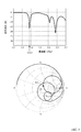
- FIG. 4 shows a frequency-standing wave ratio characteristic of the pattern antenna 1000A (upper diagram) and a Smith chart of the input impedance of the pattern antenna 1000A (lower diagram).
- FIG. 5 shows a frequency-standing wave ratio characteristic of the pattern antenna 1000B (upper diagram) and a Smith chart of the input impedance of the pattern antenna 1000A (lower diagram).
- the frequency of the use signal (the signal (electromagnetic wave) to be transmitted / received by the pattern antenna) is 925 [MHz].
- the pattern antenna 1000A has a 925 [MHz] and a standing wave ratio of -12.4 [dB].
- Z 64.9 + j ⁇ 24.1 at 925 [MHz]
- the pattern antenna 1000B has a standing wave ratio of 925 [MHz] and a standing wave ratio of ⁇ 15.7 [dB].
- an impedance matching circuit is provided between the feeding point 31B of the short-circuit portion 3B and the ground portion 1.
- the width W2 of the short-circuit portion 3B of the pattern antenna 1000B is thicker than the width of the short-circuit portion 3A of the pattern antenna 1000A. Therefore, in the plan view, in the pattern antenna 1000B, the area where the pattern of the antenna element portion 2 and the short-circuit portion 3B overlap (for example, the area of TB1 and TB2 shown in FIG. 3) is the pattern of the antenna element portion 2 of the pattern antenna 1000A. And the area where the short-circuit portion 3A overlaps (for example, the areas of TA1 and TA2 shown in FIG. 2).
- the pattern antenna 1000B has a standing wave ratio at 925 [MHz] of -15.7 [dB]
- the pattern antenna 1000A has a standing wave ratio at 925 [MHz]. This is an improvement of 3.3 [dB] over ( ⁇ 12.4 [dB]).
- the pattern antenna of the present invention it is possible to easily adjust the frequency characteristics and input impedance characteristics of the antenna so as to approach the desired characteristics only by adjusting the width of the short-circuit portion of the pattern antenna.
- the pattern antenna of the present invention As a result, with the pattern antenna of the present invention, desired antenna characteristics can be realized, impedance adjustment can be performed appropriately, and the circuit scale of the antenna circuit connected to the pattern antenna can be reduced. it can.
- the relative dielectric constant between the first surface (the surface on which the ground portion 1 and the antenna element portion 2 are formed) and the second surface (the surface on which the short-circuit portion 3 is formed) is predetermined. And adjust the input impedance of the pattern antenna 1000 by adjusting the positional relationship and shape of the antenna element portion 2 and the short-circuit portion 3 in plan view as described above. Also good.
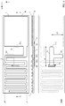
- FIG. 6 is a schematic configuration diagram of a pattern antenna 2000 according to the second embodiment.
- FIG. 6 shows a plan view (upper view) of the pattern antenna 2000 according to the second embodiment, an AA sectional view (middle view), and a bottom view (lower view) of the pattern antenna 2000. Also, as shown in FIG. 6, the X axis and the Y axis are set.
- the pattern antenna 2000 includes a substrate B, a ground portion (GND portion) 1 patterned on the first surface of the substrate B, and a meander-shaped antenna element portion connected to the ground portion 1. 2 is provided. Further, as shown in FIG. 6, the pattern antenna 2000 includes a short-circuit portion 3C and a protrusion 3D extending from the short-circuit portion 3C in the Y-axis direction on the second surface, which is the back surface of the first surface.
- the protrusion 3D is formed to have a length L3 in the Y-axis direction from a substantially center position in the width direction (Y-axis direction) of the short-circuit portion 3C.
- the length L3 may be set to a length substantially equal to ⁇ / 4, where ⁇ is the wavelength of the frequency component of a signal to be excluded (a signal that is not desired to be transmitted / received by the pattern antenna).
- the protrusion 3D is formed so as to overlap the pattern of the antenna element 2 in a plan view.
- the portion where the pattern of the short-circuit portion 3C and the pattern of the antenna element portion 2 overlap is equivalent to a capacitor installed in parallel with the feeding point 31C of the short-circuit portion 3C and the ground portion 1.
- Capacitance (capacitance component) can be added to the input impedance of the antenna 2000.
- length L3 of the protrusion 3D shown in FIG. 6 may be determined as follows.
- L3A ⁇ 0 / 4 ⁇ 0.3 ⁇ ( ⁇ 0 / 4) sqrt (x): You may make it equal to length L3A which satisfy
- the capacitance contribution ratio Kc is (1) the conductor pattern of the antenna element portion 2 and the conductor of the protrusion portion 3D in a portion where the conductor pattern of the antenna element portion 2 and the conductor pattern of the protrusion portion 3D overlap in plan view.
- the capacitance contribution rate Kc can be determined. Therefore, as described above, the shape (for example, the length L3) of the protrusion is determined based on the determined capacitance contribution rate Kc. can do.
- the length L3 of the protrusion 3D shown in FIG. 6 may be determined.
- An antenna in which the antenna element portion 2 has a complicated shape such as the pattern antenna 1000 shown in the first embodiment and the pattern antenna 2000 of the present embodiment, often has multiband characteristics.
- the standing wave ratio is small at 2.5 [GHz] in addition to the frequency 925 [MHz] of the used signal, and 2.5 [GHz]. It also shows good antenna characteristics for signals (electromagnetic waves). That is, the pattern antenna 1000B has a multiband characteristic that can satisfactorily transmit and receive a signal of frequency 925 [MHz] and a signal of 2.5 [GHz].
- the signal of 2.5 [GHz] is an unnecessary signal, and the antenna characteristics per 2.5 [GHz] are improved (per 2.5 [GHz]. It is necessary to improve the characteristics so that no signal is transmitted or received.
- the pattern antenna 2000 of the present embodiment as shown in FIG. Thereby, when it has multiband characteristics, the input impedance in the vicinity of the frequency of the unnecessary signal is changed, and the antenna transmission / reception sensitivity of the unnecessary signal is lowered.
- the pattern antenna 2000 of the present embodiment has good antenna transmission / reception sensitivity only near the frequency of the used signal, and can transmit / receive only the used signal.
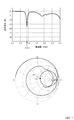
- FIG. 7 shows an antenna characteristic (example) of the pattern antenna 2000 of the present embodiment. Specifically, FIG. 7 shows the frequency-standing wave ratio characteristics (upper figure) of the pattern antenna 2000 with the protrusion 3D added to the pattern antenna 1000B having the antenna characteristics of FIG. The impedance Smith chart (lower figure) is shown.
- the pattern antenna 2000 has a 925 [MHz] and a standing wave ratio of ⁇ 17.9 [dB].
- the input impedance of the pattern antenna 2000 can be brought close to 50 [ ⁇ ].
- the frequency-standing wave ratio characteristic (upper figure) of the pattern antenna 2000 exists in the frequency-standing wave ratio characteristic (upper figure) of the pattern antenna 1000B of FIG.
- the peak around 5 [GHz] has disappeared, and multiband characteristics are not exhibited. That is, in the pattern antenna 2000, by providing the protrusion 3D, the input impedance per 2.5 [GHz] changes, and the characteristics are improved so that the signal per 2.5 [GHz] is not passed. .
- the input impedance is closer to 50 [ ⁇ ] compared to the pattern antenna of the first embodiment, it is connected to the pattern antenna in order to adjust the input impedance to 50 [ ⁇ ].
- the circuit scale of the antenna circuit can be further reduced.
- the principle that the projection antenna 3D can be prevented from receiving the signal of the unnecessary frequency (the antenna transmission / reception sensitivity of the signal of the unnecessary frequency can be lowered) is described with reference to FIG. To do.
- FIG. 8 is a diagram schematically showing signal waves w1 to w5 having unnecessary frequencies by extracting the short-circuit portion 3C and the projection portion 3D in the pattern antenna 2000.
- FIG. 8 is a diagram schematically showing signal waves w1 to w5 having unnecessary frequencies by extracting the short-circuit portion 3C and the projection portion 3D in the pattern antenna 2000.
- the signal wave w1 of the unnecessary frequency that has entered from the antenna element portion 2 side propagates to the protrusion 3D side and the feeding point side at the point A1 shown in FIG.
- the signal wave w2 having an unnecessary frequency that propagates from the point A1 to the protrusion 3D is reflected by the tip of the protrusion 3D. Since the projecting portion 3D is an open stub, the signal wave w2 is totally reflected at the open end, and thus is reflected without changing the phase (with a phase difference of 0) and propagates to the point A1 as a reflected wave w3. .
- the reflected wave w3 that has reached the point A1 is propagated as a signal wave w5 from the point A1 to the antenna element part 2 side and to the feeding point side.
- the signal wave w5 reciprocates the distance from the point A1 to the tip of the protrusion 3D, that is, propagates a distance of 2 ⁇ ⁇ 1 / 4
- the signal wave w5 is the signal wave w1. Is shifted in phase by ⁇ with respect to the signal W4 propagated to the feeding point side as it is. That is, since the signal wave w4 and the signal wave w5 are in opposite phases, the signal components of both are canceled out. As a result, an unnecessary frequency signal is not propagated to the feeding point.
- the unnecessary signal is fed to the pattern antenna 2000 by setting the distance from the center in the width direction of the short-circuit portion 3C to the tip of the protrusion 3D to 1 ⁇ 4 of the wavelength of the unnecessary signal. Propagation to the point side can be prevented.
- the antenna transmission / reception sensitivity of the unnecessary frequency component can be deteriorated, and the antenna characteristics of the pattern antenna 2000 can be improved.
- the antenna sensitivity to the electromagnetic waves to be excluded may be reduced in consideration of the wavelength shortening effect.
- the wavelength shortening effect means that when a high-frequency signal (high-frequency electromagnetic wave) passes through the conductor, the high-frequency signal passes through the conductor due to the influence of the relative permittivity of the material around the conductor. This means the effect of shortening the wavelength of the high-frequency signal.
- the position of the protrusion 3D of the pattern antenna 2000 may be other than the position described above.
- a protrusion may be formed to extend from the short-circuit portion 3C at any position 3F to 3I shown in FIG.
- the protrusions may be formed at any two or more positions indicated by 3D to 3I in FIG.
- a protrusion may be formed so as to extend from the short-circuit portion 3C in an arbitrary direction (for example, an oblique direction).
- the signal from the point on the center line in the width direction (Y-axis direction) of the short-circuit portion 3C to the tip of the protruding portion extending in an arbitrary direction is not desired to be transmitted / received by an antenna, for example.
- the wavelength By setting the wavelength to about 1/4 of the signal to be removed, the signal component (the signal component of the unnecessary signal) can be efficiently removed.
- the protruding portion 3D extending from the short-circuit portion 3C can efficiently remove unnecessary signals, improve the antenna characteristics, and provide capacitance (capacitance component).
- the input impedance is also close to the desired value.
- the first surface of the substrate B (the surface on which the ground portion 1 and the antenna element portion 2 are formed) and the second surface (the surface on which the short-circuit portion 3C and the protruding portions 3D (3E to 3I) are formed).
- the relative dielectric constant between the antenna element portion 2 and the short-circuit portion 3 in the plan view is adjusted as described above, and the positional relationship and shape of the antenna element portion 2 and the short-circuit portion 3 are adjusted as described above.
- the input impedance may be adjusted.
Landscapes
- Details Of Aerials (AREA)
- Waveguide Aerials (AREA)
Abstract
所望のアンテナ特性を有し、かつ、小さい面積の領域にも形成することができるパターンアンテナを実現する。パターンアンテナ(1000)は、基板(B)と、基板(B)の第1面に形成されたグランド部(1)と、アンテナ素子部(2)と、短絡部(3)と、接続部(V1)と、を備える。アンテナ素子部(2)は、基板の第1面に、折り曲げ部が複数形成されるように設けられた導体パターンであって、グランド部(1)と電気的に接続されている導体パターンを含む。短絡部(3)は、第1面のアンテナ素子部(2)の導体パターンと、基板(B)の第1面とは異なる面である第2面に、平面視において、アンテナ素子部(2)の導体パターンの少なくとも一部と重なるように設けられた導体パターンを含む。接続部(V1)は、アンテナ素子部(2)の導体パターンと、短絡部(3)の導体パターンとを電気的に接続する。
Description
本発明は、パターンアンテナおよびパターンアンテナを備えるアンテナ装置に関する。
近年、小型機器に無線機能が搭載されることが多くなっており、当該小型機器に搭載するためのアンテナの小型化の要求が高まっている。
従来より、小型機器に搭載するためのアンテナとして、F字型のパターンアンテナが広く用いられている。F字型のパターンアンテナは、プリント基板の表面に、アンテナ素子を、F字型となるようにパターン形成させることで構成される。これにより、プリント基板上の比較的小さい面積の部分において、高周波用のアンテナを形成することができる。
また、F字型のパターンアンテナにおいて、アンテナ素子の形状(プリント基板上のパターン形状)を変形させて、アンテナ特性を改善する技術も提案されている(例えば、特許文献1(特開2009-194783号公報)を参照)。
しかしながら、上記従来の技術では、所望のアンテナ特性のアンテナを実現するのが困難な場合がある。これについて、図10を用いて説明する。
図10は、従来のF字型パターンアンテナ900の一例を示す図である。図10に示すように、F字型パターンアンテナ900は、基板91と、基板91上にパターン形成されたグランド面92と、グランド面92に接続されたアンテナ素子93と、を備える。また、F字型パターンアンテナ900は、図10に示すように、給電点94、95を備える。
F字型パターンアンテナ900で使用する搬送波の波長をλとすると、図10のアンテナ素子93の長さL91を約λ/4とすることで、良好なアンテナ特性(周波数特性)を得ることができる。また、F字型パターンアンテナ900において、入力インピーダンスを50Ωに整合しようとする場合、給電点94からGND面までの距離(図10に矢印M1で示した部分の距離)と、給電点94の位置(図10にL92で示した長さ)と調整することで、キャパシタンス成分およびインダクタンス成分が調整され、入力インピーダンスを50Ωに近づけることができる。
図10に示すF字型パターンアンテナ900では、アンテナ素子93が、図10の縦方向に延びる構成を有しており、長さL91を約λ/4の長さにする必要があるので、より小さい面積の領域に、F字型パターンアンテナ900のアンテナ性能を維持しつつ、パターンアンテナを構成するのは困難である。
そこで、図11に示すパターンアンテナ900Aのように、アンテナ素子部分を折り曲げることで(アンテナ素子部分をメアンダ状に形成することで)、アンテナ素子部分の長さを確保しつつ、より小さい面積の領域にパターンアンテナを構成することが考えられる。
しかしながら、図11に示すパターンアンテナ900Aでは、アンテナ素子部93Aの最もGND面92A側のメアンダ状の部分から給電点94Aに向かって延びる短絡部931Aに必要な領域が狭くなる。つまり、図11に示すように、短絡部931Aの位置を調整できる範囲が限定されるので、パターンアンテナ900Aでは、短絡部931Aの位置を調整し、所望のアンテナ特性を得ることや、適切にインピーダンス整合をとることが困難となる。
そこで、本発明は、上記問題点に鑑み、所望のアンテナ特性を有し、かつ、小さい面積の領域にも形成することができるパターンアンテナを実現することを目的とする。
上記課題を解決するために、第1の発明は、基板と、基板の第1面に形成されたグランド部と、アンテナ素子部と、短絡部と、接続部と、を備えるパターンアンテナである。
アンテナ素子部は、基板の第1面に、折り曲げ部が複数形成されるように設けられた導体パターンであって、グランド部と電気的に接続されている導体パターンを含む。
短絡部は、第1面のアンテナ素子部の導体パターンと、基板の第1面とは異なる面である第2面に、平面視において、アンテナ素子部の導体パターンの少なくとも一部と重なるように設けられた導体パターンを含む。
接続部は、アンテナ素子部の導体パターンと、短絡部の導体パターンとを電気的に接続する。
このパターンアンテナでは、アンテナ素子部の導体パターンが、基板の第1面に、折り曲げ部が複数形成されるように設けられているので、必要なアンテナの導体パターンの長さを確保しつつ、小さい面積の領域にアンテナ素子部を設けることができる。また、このパターンアンテナでは、短絡部が、基板の第1面のアンテナ素子部と電気的に接続されており、かつ、基板の第2面に形成されているので、小さい面積においても、十分な大きさ(長さ)の短絡部を形成することができる。そして、このパターンアンテナでは、平面視で、短絡部の導体パターンとアンテナ素子部の導体パターンとの重なり具合を調整することで、入力インピーダンスに容量性(キャパシタンス成分)を付与することができる。
したがって、このパターンアンテナでは、所望のアンテナ特性を実現しやすく、また、入力インピーダンス調整もしやすい。その結果、インピーダンス調整のために必要となる送受信回路の回路規模を低減させることができる。つまり、このパターンアンテナでは、パターンアンテナを形成するのに必要な面積を小さくすることができ、かつ、所望のアンテナ特性を容易に実現させることができる。
なお、基板は、多層基板であってもよく、基板の一層に第1面が形成され、別の一層に第2面が形成されていてもよい。
第2の発明は、第1の発明であって、アンテナ素子部は、メアンダ状に形成された導体パターンを含む。
これにより、このパターンアンテナでは、アンテナ素子部の導体パターンがメアンダ状に形成されるため、アンテナ素子部を小さい面積の領域に構成することができる。
第3の発明は、第1または第2の発明であって、基板の第2面において、短絡部に電気的に接続され、平面視において、アンテナ素子部の導体パターンの少なくとも一部と重なるように形成された導体パターンを含む突起部をさらに備える。
これにより、このパターンアンテナでは、不要な信号(電磁波)に対するアンテナ感度を低減させることができる。つまり、アンテナ素子部が複雑な形状である場合に、マルチバンド特性となることがある。このような場合であっても、このパターンアンテナでは、突起部を設け、当該突起部の形状および位置を調整することで、不要な信号(電磁波)に対するアンテナ感度を低減させることができる。その結果、このパターンアンテナでは、マルチバンド特性となることを適切に防止することができる。
また、このパターンアンテナでは、平面視における突起部の導体パターンと、アンテナ素子部の導体パターンとの重なり具合を調整することで、所望の容量性(キャパシタンス成分)を付与することができる。したがって、このパターンアンテナでは、所望のアンテナ特性を容易に実現することができる。
第4の発明は、第3の発明であって、短絡部および突起部は、矩形状である。
突起部は、短絡部の平面視における長手方向の中心線から、突起部の先端部までの距離が、パターンアンテナで除外する対象とする電磁波の波長をλとすると、λ/4±0.3×(λ/4)を満たす長さとなるように形成されている。
これにより、このパターンアンテナでは、短絡部から突起部の先端部で全反射して戻ってきた波長λの電磁波(除外対象の電磁波)と、短絡部から給電点(アンテナ送受信部を接続するための短絡部上の接続点)に伝搬する波長λの電磁波(除外対象の電磁波)との位相差が約πとなり、逆相となる。つまり、直接給電点へ伝搬される波長λの電磁波と、突起部で全反射して給電点へ伝搬される波長λの電磁波とは、相殺される。その結果、このパターンアンテナでは、除外対象の電磁波に対するアンテナ感度を低減させることができる。
第5の発明は、第3の発明であって、短絡部および突起部は、矩形状である。
突起部は、
基板の比誘電率をεrとし、
短絡部の平面視における長手方向の中心線から、突起部の先端部までの距離が、パターンアンテナで除外する対象とする電磁波の波長をλとすると、
λ0=λ/sqrt(εr)
L1=λ0/4±0.3×(λ0/4)
sqrt(x):xの平方根を取得する関数
を満たす長さL1となるように形成されている。
基板の比誘電率をεrとし、
短絡部の平面視における長手方向の中心線から、突起部の先端部までの距離が、パターンアンテナで除外する対象とする電磁波の波長をλとすると、
λ0=λ/sqrt(εr)
L1=λ0/4±0.3×(λ0/4)
sqrt(x):xの平方根を取得する関数
を満たす長さL1となるように形成されている。
これにより、このパターンアンテナでは、波長短縮効果を考慮して、除外対象の電磁波に対するアンテナ感度を低減させることができる。
波長短縮効果とは、高周波信号(高周波数の電磁波)が導体部分を通過する場合に、当該高周波信号が、通過する導体部分の周辺の物質の比誘電率の影響を受けて、導体部分を通過する高周波信号の波長が短縮する効果をいう。波長短縮効果を考慮した波長λ0は、通過する導体部分の周辺の物質の比誘電率をεrとすると、λ0=λ/sqrt(εr)により算出される。
第6の発明は、第3の発明であって、短絡部および突起部は、矩形状である。
突起部は、
基板の比誘電率をεrとし、
平面視において、アンテナ素子部の導体パターンと、突起部の導体パターンが重なることで生じるキャパシタンス寄与率をKc(0≦Kc≦1)とし、
短絡部の平面視における長手方向の中心線から、突起部の先端部までの距離が、パターンアンテナで除外する対象とする電磁波の波長をλとすると、
λ0=λ/sqrt(εr)
L2=Kc×λ0/4±0.3×Kc×(λ0/4)
sqrt(x):xの平方根を取得する関数
を満たす長さL2となるように形成されている。
基板の比誘電率をεrとし、
平面視において、アンテナ素子部の導体パターンと、突起部の導体パターンが重なることで生じるキャパシタンス寄与率をKc(0≦Kc≦1)とし、
短絡部の平面視における長手方向の中心線から、突起部の先端部までの距離が、パターンアンテナで除外する対象とする電磁波の波長をλとすると、
λ0=λ/sqrt(εr)
L2=Kc×λ0/4±0.3×Kc×(λ0/4)
sqrt(x):xの平方根を取得する関数
を満たす長さL2となるように形成されている。
これにより、このパターンアンテナでは、波長短縮効果を考慮し、さらに、平面視において、アンテナ素子部の導体パターンと、突起部の導体パターンが重なることで生じるキャパシタンス寄与率をKc(0≦Kc≦1)をも考慮して、除外対象の電磁波に対するアンテナ感度を低減させることができる。
平面視において、アンテナ素子部の導体パターンと、突起部の導体パターンが重なることでパターンアンテナの入力インピーダンスに容量成分(キャパシタンス成分)が付与されるため、このパターンアンテナでは、当該容量成分(キャパシタンス成分)の影響を考慮したキャパシタンス寄与率Kcを用いて、上記数式により長さL2を決定することで、除外対象の電磁波に対するアンテナ感度を低減させるとともに、さらに、突起部の大きさを小さくすることができる。その結果、このパターンアンテナでは、より小さい面積により構成でき、かつ、除外対象の電磁波に対するアンテナ感度を適切に低減することができる。
第7の発明は、第3から第6のいずれかの発明であって、基板の第2面において、突起部が、互いに重ならないように、複数形成されている。
これにより、このパターンアンテナでは、複数の突起部により、例えば、複数の不要な周波数の電磁波に対するアンテナ感度を低減させることができる。また、このパターンアンテナでは、平面視で、複数の突起部の導体パターンと、アンテナ素子部の導体パターンとの重なり具合を調整することで、所望の容量性(キャパシタンス成分)を付与することができる。したがって、このパターンアンテナでは、所望のアンテナ特性を容易に実現することができる。
本発明によれば、所望のアンテナ特性を有し、かつ、小さい面積の領域にも形成することができるパターンアンテナを実現することを目的とする。
[第1実施形態]
第1実施形態について、図面を参照しながら、以下、説明する。
第1実施形態について、図面を参照しながら、以下、説明する。
図1は、第1実施形態に係るパターンアンテナ1000の概略構成図である。
図1に、第1実施形態のパターンアンテナ1000の平面図(上段の図)と、A-A断面図(中段の図)と、上記パターンアンテナ1000の底面図(下段の図)とを示す。また、図1に示すように、X軸、Y軸を設定する。
パターンアンテナ1000は、図1に示すように、基板Bと、基板Bの第1面上にパターン形成されたグランド部(GND部)1と、グランド部1に接続されたメアンダ状のアンテナ素子部2と、を備える。また、パターンアンテナ1000は、図1に示すように、第1面の裏面である第2面上に、短絡部3と、を備える。
基板Bは、例えば、プリント基板(例えば、ガラスエポキシ基板)であり、第1面および第2面(第1面とは異なる面)上に、導体(例えば、銅箔)によりパターンを形成することができる。基板Bは、例えば、比誘電率が4.3程度の素材(例えば、ガラスエポキシ樹脂)により形成されている。図1では、第1面が基板Bの表面であり、第2面が第1面と反対側の表面(裏面)である場合を示しているが、これに限定されることはない。基板Bは、多層基板であってもよく、基板Bの一層に第1面が形成され、別の一層に第2面が形成されていてもよい。以下では、説明便宜のため、図1の場合(第1面が基板Bの表面であり、第2面が第1面と反対側の表面(裏面)である場合)について、説明する。
グランド部1は、基板Bの第1面上に形成されたパターンであり、GND電位と接続される。
アンテナ素子部2は、基板Bの第1面上に形成されたメアンダ状のパターン(折り曲げ部が繰り返し形成されているパターン)である。アンテナ素子部2は、図1に示すように、グランド部1の端部から、折り曲げ部を繰り返し形成しながら、X軸正方向に延びるように形成されたパターンである。アンテナ素子部2のパターンは、導体(例えば、銅箔)により形成されている。
また、アンテナ素子部2は、図1に示すように、アンテナ素子部2のパターン上において、第2面と電気的に接続させるためのスルーホール(ビアホール)V1が形成されている。なお、スルーホールV1は、アンテナ素子部2のメアンダ状のパターンのY軸方向の第1端(図1に、Y座標「y0」で示した端部)と第2端(図1に、Y座標「y1」で示した端部)との中点を通り、X軸に平行な線と、アンテナ素子部2のパターンとが交差する交点付近に設けられることが好ましい。
短絡部3は、基板Bの第2面上に形成されており、第2面のおけるスルーホールV1を含む位置からX軸負方向(グランド部1への方向)に延びるパターンである。短絡部3のパターンは、導体(例えば、銅箔)により形成されている。短絡部3は、スルーホールV1に、例えば、半田等の導体を充填することで、第1面のアンテナ素子部2と電気的に接続される。
また、平面視で、短絡部3のグランド部1側の端部付近と、グランド部1との間に、アンテナ送受信部(例えば、アンテナ送受信用回路)が設置される。
例えば、パターンアンテナ1000を送信アンテナとして機能させる場合、短絡部3の給電点31と、グランド部1との間に、送信部(例えば、アンテナ用送信回路)を接続する。また、例えば、パターンアンテナ1000を受信アンテナとして機能させる場合、短絡部3の給電点31と、グランド部1との間に、受信部(例えば、アンテナ用受信回路)を接続する。
なお、給電点31は、一例であり、上記に限定されない。例えば、短絡部3のグランド部1側の端部の他の部分を給電点としてもよい。また、給電点は、点に限定されず、線状の領域や面状の領域(例えば、短絡部3のグランド部1側の端点の側面の一部または全部の領域)であってもよい。
以上のように構成されたパターンアンテナ1000では、短絡部3が、アンテナ素子部2のパターンが形成されている第1面とは別の第2面に形成されているので、短絡部3の長さを長くすることができる。例えば、図11に示す、第1面のみにアンテナ素子部93Aと短絡部931Aとを形成させた場合の短絡部931Aの長さd9に比べて、パターンアンテナ1000では、図1に示すように、短絡部3の長さd1をかなり長くすることができる。
これにより、パターンアンテナ1000では、アンテナ特性を改善することができる。つまり、パターンアンテナ1000では、第1面のアンテナ素子部2と、第2面の短絡部3とが、基板B(例えば、比誘電率が4.3程度の基板)を挟んで、配置されており、平面視において、第1面のアンテナ素子部2の一部と、第2面の短絡部3の一部とが重なるので、容量結合を生じさせることができる。具体的には、図1のA-A断面図(中段の図)の領域AR1、AR2およびAR3において、アンテナ素子部2の導体パターンと、短絡部3の導体パターンとが、基板Bを挟んで配置されており、この領域AR1、AR2およびAR3において、アンテナ素子部2とグランド部1との間に、並列にコンデンサが挿入されているのと等価であると考えることができる。したがって、パターンアンテナ1000では、図1に示すように、短絡部3を形成することで、容量結合を生じさせることができ、その結果、アンテナ特性を改善させることができる。また、パターンアンテナ1000では、短絡部3の幅を調整することで、容量結合の程度を調整することができるため、所望のアンテナ特性を取得しやすい。さらに、パターンアンテナ1000では、短絡部3を、第1面とは別の第2面に形成しているので、短絡部を形成するために必要な面積を小さくすることができ、その結果、所望のアンテナ特性を実現するパターンアンテナ1000を小さな面積に構成することができる。
従来技術では、アンテナ特性を改善させる、あるいは、インピーダンス調整を行うために、アンテナとは、別に、LC回路を設ける必要があった。それに対して、パターンアンテナ1000では、図1に示すように、短絡部3を形成することで、容量結合を生じさせることができるので、従来、所望のアンテナ特性を実現させるために、あるいは、インピーダンス調整を行うために必要であったLC回路等を不要にする、あるいは、その回路規模を小さくすることができる。つまり、パターンアンテナ1000では、所望のアンテナ特性を実現することができ、また、インピーダンス調整を適切に行うことができるとともに、パターンアンテナ1000に接続するアンテナ用回路の回路規模を低減させることができる。
≪インピーダンス調整≫
次に、第1の実施形態のパターンアンテナ1000におけるインピーダンス調整(目標インピーダンスを50[Ω]とする。)について、以下、説明する。
次に、第1の実施形態のパターンアンテナ1000におけるインピーダンス調整(目標インピーダンスを50[Ω]とする。)について、以下、説明する。
図2は、第1の実施形態のパターンアンテナの一例であるパターンアンテナ1000Aの平面図(図1の上段の図と同様の図)である。図2のパターンアンテナ1000Aにおいて、アンテナ素子部2の長手方向の長さL1(図2にL1で示した長さ)が、33.4[mm]であり、アンテナ素子部2の幅W1(図2にW1で示した長さ)が、15.8[mm]であり、短絡部3の長手方向の長さL2(図2にL2で示した長さ)が、14.7[mm]であり、短絡部3Aの幅W2(図2にW2で示した長さ)が、1.85[mm]である。
図3は、第1の実施形態のパターンアンテナの一例であるパターンアンテナ1000Bの平面図(図1の上段の図と同様の図)である。図3のパターンアンテナ1000Bにおいて、アンテナ素子部2の長手方向の長さL1(図2にL1で示した長さ)は、図2の場合と同じで、33.4[mm]であり、アンテナ素子部2の幅W1(図2にW1で示した長さ)は、図2の場合と同じで、15.8[mm]である。短絡部3の長手方向の長さL2(図2にL2で示した長さ)は、図2の場合と同じで、14.7[mm]であり、短絡部3Bの幅W2(図2にW2で示した長さ)は、2.92[mm]である。なお、図3では、パターンアンテナ1000Bの短絡部3Bは、平面視で、グランド部1側の端部の形状が、円弧状であるが、これに限定されることはなく、短絡部3Bは、平面視で矩形状であってもよい。
また、図4に、パターンアンテナ1000Aの周波数-定在波比特性(上図)、および、パターンアンテナ1000Aの入力インピーダンスのスミスチャート図(下図)を示す。
また、図5に、パターンアンテナ1000Bの周波数-定在波比特性(上図)、および、パターンアンテナ1000Aの入力インピーダンスのスミスチャート図(下図)を示す。
なお、パターンアンテナ1000Aおよび1000Bでは、使用信号(パターンアンテナにより送受信しようとする信号(電磁波))の周波数が925[MHz]であるものとして、以下、説明する。
図4の周波数-定在波比特性(上図)から分かるように、パターンアンテナ1000Aでは、925[MHz]で、定在波比が-12.4[dB]である。
図4の入力インピーダンスのスミスチャート図(下図)におけるK1点は、925[MHz]におけるパターンアンテナ1000Aの入力インピーダンスを示している。つまり、925[MHz]における、パターンアンテナ1000Aの入力インピーダンスZは、複素表現で、
Z=64.9+j×24.1
j:虚数単位
であり、パターンアンテナ1000Aの入力インピーダンス(Zの絶対値)は、69.1[Ω]である。
Z=64.9+j×24.1
j:虚数単位
であり、パターンアンテナ1000Aの入力インピーダンス(Zの絶対値)は、69.1[Ω]である。
パターンアンテナ1000Aでは、例えば、短絡部3Aの給電点31Aとグランド部1との間に、インピーダンス整合用の回路を設け、925[MHz]において、Z=64.9+j×24.1が、Z=50となるように、調整することで、パターンアンテナ1000Aの入力インピーダンスを50[Ω]に近づけることができる。
また、図5の周波数-定在波比特性(上図)から分かるように、パターンアンテナ1000Bでは、925[MHz]で、定在波比が-15.7[dB]である。
図5の入力インピーダンスのスミスチャート図(下図)におけるK2点は、925[MHz]におけるパターンアンテナ1000Bの入力インピーダンスを示している。つまり、925[MHz]における、パターンアンテナ1000Bの入力インピーダンスZは、複素表現で、
Z=63.5+j×12.9
j:虚数単位
であり、パターンアンテナ1000Bの入力インピーダンス(Zの絶対値)は、64.9[Ω]である。
Z=63.5+j×12.9
j:虚数単位
であり、パターンアンテナ1000Bの入力インピーダンス(Zの絶対値)は、64.9[Ω]である。
パターンアンテナ1000Bでは、例えば、短絡部3Bの給電点31Bとグランド部1との間に、インピーダンス整合用の回路を設け、925[MHz]において、Z=63.5+j×12.9が、Z=50となるように、調整することで、パターンアンテナ1000Bの入力インピーダンスを50[Ω]に近づけることができる。
図2、図3から分かるように、パターンアンテナ1000Bの短絡部3Bの幅W2は、パターンアンテナ1000Aの短絡部3Aの幅よりも太い。したがって、平面視において、パターンアンテナ1000Bでは、アンテナ素子部2のパターンと短絡部3Bとが重なる面積(例えば、図3に示すTB1、TB2の面積)が、パターンアンテナ1000Aのアンテナ素子部2のパターンと短絡部3Aとが重なる面積(例えば、図2に示すTA1、TA2の面積)よりも大きい。その結果、パターンアンテナ1000Bでは、パターンアンテナ1000Aに比べて、短絡部3Bの給電点31Bとグランド部1との間に並列に挿入される容量成分(キャパシタンス成分)が大きくなる。つまり、925[MHz]において、パターンアンテナ1000Aの入力インピーダンスは、Z=64.9+j×24.1であるが、パターンアンテナ1000Bの入力インピーダンスは、Z=63.5+j×12.9であり、容量性が付与され(虚数部の値が小さくなっており)、より目標入力インピーダンスである50[Ω]に近くなっている。
また、図4,図5から分かるように、パターンアンテナ1000Bでは、925[MHz]における定在波比が-15.7[dB]であり、パターンアンテナ1000Aの925[MHz]における定在波比(-12.4[dB])よりも、3.3[dB]改善されている。
このように、本発明のパターンアンテナでは、パターンアンテナの短絡部の幅を調整するだけで、アンテナの周波数特性および入力インピーダンス特性が所望の特性に近づくように、容易に調整することができる。
その結果、本発明のパターンアンテナでは、所望のアンテナ特性を実現することができ、また、インピーダンス調整を適切に行うことができるとともに、パターンアンテナに接続するアンテナ用回路の回路規模を低減させることができる。
なお、基板Bの第1面(グランド部1とアンテナ素子部2とが形成されている面)と、第2面(短絡部3が形成されている面)との間の比誘電率を所定の値となるように調整し、上記のように、平面視における、アンテナ素子部2と、短絡部3との位置関係や形状等を調整し、パターンアンテナ1000の入力インピーダンスを調整するようにしてもよい。
[第2実施形態]
次に、第2実施形態について、図面を参照しながら、以下、説明する。
次に、第2実施形態について、図面を参照しながら、以下、説明する。
なお、本実施形態において、第1実施形態と同様の部分については、同一符号を付し、詳細な説明を省略する。
図6は、第2実施形態に係るパターンアンテナ2000の概略構成図である。
図6に、第2実施形態のパターンアンテナ2000の平面図(上段の図)と、A-A断面図(中段の図)と、上記パターンアンテナ2000の底面図(下段の図)とを示す。また、図6に示すように、X軸、Y軸を設定する。
パターンアンテナ2000は、図6に示すように、基板Bと、基板Bの第1面上にパターン形成されたグランド部(GND部)1と、グランド部1に接続されたメアンダ状のアンテナ素子部2と、を備える。また、パターンアンテナ2000は、図6に示すように、第1面の裏面である第2面上に、短絡部3Cと、短絡部3CからY軸方向に延びた突起部3Dと、を備える。
突起部3Dは、図6に示すように、短絡部3Cの幅方向(Y軸方向)の略中心位置からY軸方向に長さL3を有するように形成されている。長さL3は、例えば、除外したい信号(パターンアンテナで送受信したくない信号)の周波数成分の波長をλとすると、λ/4と略等しい長さにするようにしてもよい。
また、突起部3Dは、図6に示すように、平面視において、アンテナ素子部2のパターンと重なるように、形成されている。これにより、平面視で、短絡部3Cのパターンとアンテナ素子部2のパターンとの重なっている部分が、短絡部3Cの給電点31Cとグランド部1と並列に設置されたコンデンサと等価となり、パターンアンテナ2000の入力インピーダンスに容量性(キャパシタンス成分)を付与することができる。
なお、図6に示した、突起部3Dの長さL3は、以下のように、決定されるものであってもよい。
基板Bの比誘電率をεrとすると、
長さL3は、
λ0=λ/sqrt(εr)
L3A=λ0/4±0.3×(λ0/4)
sqrt(x):xの平方根を取得する関数
を満たす長さL3Aと等しくなるようにしてもよい。
長さL3は、
λ0=λ/sqrt(εr)
L3A=λ0/4±0.3×(λ0/4)
sqrt(x):xの平方根を取得する関数
を満たす長さL3Aと等しくなるようにしてもよい。
さらに、平面視で、アンテナ素子部2の導体パターンと、突起部3Dの導体パターンが重なることで生じるキャパシタンス寄与率をKc(0≦Kc≦1)とすると、
長さL3は、
λ0=λ/sqrt(εr)
L3B=Kc×λ0/4±0.3×Kc×(λ0/4)
sqrt(x):xの平方根を取得する関数
を満たす長さL3Bと等しくなるようにしてもよい。
長さL3は、
λ0=λ/sqrt(εr)
L3B=Kc×λ0/4±0.3×Kc×(λ0/4)
sqrt(x):xの平方根を取得する関数
を満たす長さL3Bと等しくなるようにしてもよい。
例えば、パターンアンテナ2000の大きさが、図3に示したパターンアンテナ1000Bと同様である場合、一例として、
λ=c/f
(c:光速、f:除外したい信号の周波数)
f=2.5[GHz]
Kc=0.55
εr=4.3
とすると、
λ0=λ/sqrt(εr)=0.03/sqrt(4.3)≒57.97[mm]
L3B=Kc×λ0/4
=0.55×λ0/4
≒0.55×57.97/4[mm]
≒0.55×57.97/4[mm]
≒8[mm]
である。
λ=c/f
(c:光速、f:除外したい信号の周波数)
f=2.5[GHz]
Kc=0.55
εr=4.3
とすると、
λ0=λ/sqrt(εr)=0.03/sqrt(4.3)≒57.97[mm]
L3B=Kc×λ0/4
=0.55×λ0/4
≒0.55×57.97/4[mm]
≒0.55×57.97/4[mm]
≒8[mm]
である。
したがって、上記の場合、L3≒8[mm]とすることで、周波数が2.5[GHz]付近の不要信号を適切に除外することができる。つまり、パターンアンテナ2000において、周波数が2.5[GHz]付近の不要信号のアンテナ感度を適切に低減することができる。
なお、キャパシタンス寄与率Kcは、平面視で、アンテナ素子部2の導体パターンと、突起部3Dの導体パターンとが重なる部分における、(1)アンテナ素子部2の導体パターンと、突起部3Dの導体パターンとの間の物質(例えば、基板B)の比誘電率や、(2)平面視で、アンテナ素子部2の導体パターンと、突起部3Dの導体パターンとが重なる部分の面積等に決定される。
つまり、パターンアンテナの構成が決定されれば、キャパシタンス寄与率Kcは決定できるので、決定されたキャパシタンス寄与率Kcに基づいて、上記のように、突起部の形状(例えば、長さL3)を決定することができる。
以上のように、図6に示した、突起部3Dの長さL3を決定してもよい。
第1実施形態で示したパターンアンテナ1000や本実施形態のパターンアンテナ2000のように、アンテナ素子部2が複雑な形状をしているアンテナは、マルチバンド特性となることが多い。例えば、図4のアンテナ特性から分かるように、パターンアンテナ1000Bでは、使用信号の周波数925[MHz]以外に、2.5[GHz]において、定在波比が小さく、2.5[GHz]の信号(電磁波)に対しても良好なアンテナ特性を示している。つまり、パターンアンテナ1000Bは、周波数925[MHz]の信号と、2.5[GHz]の信号を良好に送受信することができるマルチバンド特性を有している。しかしながら、周波数925[MHz]の信号のみを使用したい場合、2.5[GHz]の信号は、不要信号であり、2.5[GHz]あたりのアンテナ特性を改善(2.5[GHz]あたりの信号が送受信されないように特性を改善)する必要がある。
そこで、本実施形態のパターンアンテナ2000では、図6に示すように、突起部3Dを設けている。これにより、マルチバンド特性を有する場合に、不要信号の周波数付近における入力インピーダンスを変化させ、当該不要信号のアンテナ送受信感度を低下させる。
これにより、本実施形態のパターンアンテナ2000では、使用信号の周波数付近においてのみ良好なアンテナ送受信感度を有し、当該使用信号のみを送受信することができる。
図7に、本実施形態のパターンアンテナ2000のアンテナ特性(一例)を示す。具体的には、図7は、図5のアンテナ特性を有するパターンアンテナ1000Bにおいて、突起部3Dを追加したパターンアンテナ2000の周波数-定在波比特性(上図)、および、パターンアンテナ2000の入力インピーダンスのスミスチャート図(下図)を示している。
図7の周波数-定在波比特性(上図)から分かるように、パターンアンテナ2000では、925[MHz]で、定在波比が-17.9[dB]である。
図7の入力インピーダンスのスミスチャート図(下図)におけるK3点は、925[MHz]におけるパターンアンテナ2000の入力インピーダンスを示している。つまり、925[MHz]における、パターンアンテナ2000の入力インピーダンスZは、複素表現で、
Z=63.6+j×5.0
j:虚数単位
であり、パターンアンテナ2000の入力インピーダンス(Zの絶対値)は、63.8[Ω]である。
Z=63.6+j×5.0
j:虚数単位
であり、パターンアンテナ2000の入力インピーダンス(Zの絶対値)は、63.8[Ω]である。
パターンアンテナ2000では、例えば、短絡部3Cの給電点31Cとグランド部1との間に、インピーダンス整合用の回路を設け、925[MHz]において、Z=63.6+j×5.0が、Z=50となるように、調整することで、パターンアンテナ2000の入力インピーダンスを50[Ω]に近づけることができる。
また、図7から分かるように、パターンアンテナ2000の周波数-定在波比特性(上図)では、図5のパターンアンテナ1000Bの周波数-定在波比特性(上図)において存在していた2.5[GHz]あたりのピークがなくなっており、マルチバンド特性を示さなくなっている。つまり、パターンアンテナ2000では、突起部3Dを設けたことにより、2.5[GHz]あたりの入力インピーダンスが変化し、2.5[GHz]あたりの信号を通過させないように特性が改善されている。
さらに、突起部3Dを設けたことにより容量性(キャパシタンス成分)が付加され、925[MHz]における、パターンアンテナ2000の入力インピーダンスも改善されている(図5の場合に比べて、入力インピーダンスの虚数成分が小さなっている)。
これにより、パターンアンテナ2000では、第1実施形態のパターンアンテナに比べてさらに入力インピーダンスが50[Ω]に近づいているので、入力インピーダンスを50[Ω]に調整するために、パターンアンテナに接続するアンテナ用回路の回路規模をさらに低減させることができる。
なお、ここで、パターンアンテナ2000において、突起部3Dを設けることで、不要周波数の信号を受信しないようにできる(不要周波数の信号のアンテナ送受信感度を低くできる)原理について、図8を用いて説明する。
図8は、パターンアンテナ2000における短絡部3Cと、突起部3Dとを抽出し、不要周波数の信号波w1~w5を模式的に示した図である。
図8に示すように、アンテナ素子部2側から入射してきた不要周波数の信号波w1は、図8に示すA1点で、突起部3D側と、給電点側へと伝搬する。
ここで、A1点から突起部3Dの先端までのY軸方向の距離をL3とし、不要周波数の信号波の波長をλ1とすると、
L3=λ1/4
であるものとする。
L3=λ1/4
であるものとする。
A1点から突起部3D側へ伝搬する不要周波数の信号波w2は、突起部3Dの先端部で反射する。突起部3Dは、オープンスタブであるので、信号波w2は、開放端で全反射するので、位相が変化せずに(位相差0で)反射し、反射波w3として、A1点へと伝搬する。
A1点に到達した反射波w3は、A1点からアンテナ素子部2側と、給電点側に信号波w5として伝搬される。
ここで、信号波w5は、A1点から突起部3Dの先端までの距離を往復しているので、つまり、2×λ1/4の距離を伝搬しているので、信号波w5は、信号波w1がそのまま給電点側に伝搬された信号W4に対して、πだけ位相がずれている。つまり、信号波w4と信号波w5とは逆相であるので、両者の信号成分は相殺される。その結果、給電点へは、不要周波数の信号が伝搬されない。
このように、パターンアンテナ2000において、短絡部3Cの幅方向の中心から突起部3Dの先端までの距離を不要信号の波長の1/4にすることで、当該不要信号が、パターンアンテナ2000の給電点側に伝搬されることを防止することができる。
これにより、パターンアンテナ2000において、上記のように突起部3Dを設けることで、不要周波数成分のアンテナ送受信感度を劣化させ、パターンアンテナ2000のアンテナ特性を改善することができる。
さらに、パターンアンテナ2000において、波長短縮効果を考慮して、除外対象の電磁波に対するアンテナ感度を低減させるようにしてもよい。
波長短縮効果とは、高周波信号(高周波数の電磁波)が導体部分を通過する場合に、当該高周波信号が、通過する導体部分の周辺の物質の比誘電率の影響を受けて、導体部分を通過する高周波信号の波長が短縮する効果をいう。波長短縮効果を考慮した波長λ0は、通過する導体部分の周辺の物質の比誘電率をεrとすると、λ0=λ/sqrt(εr)により算出される。
さらに、平面視において、アンテナ素子部2の導体パターンと、突起部3Dの導体パターンが重なることで生じるキャパシタンス寄与率をKc(0≦Kc≦1)をも考慮して、除外対象の電磁波に対するアンテナ感度を低減させるようにしてもよい。
また、パターンアンテナ2000の突起部3Dの位置は、上記で説明した位置以外でもよい。例えば、図9に示した3F~3Iのいずれかの位置に、短絡部3Cから延びるように、突起部を形成するようにしてもよい。また、図9において3D~3Iで示した、いずれか2つ以上の位置に突起部を形成するようにしてもよい。
さらに、短絡部3Cから、任意の方向(例えば、斜め方向)に延びるように、突起部が形成されてもよい。
上記のいずれの場合においても、短絡部3Cの幅方向(Y軸方向)の中心線上の点から、任意の方向に延びた突起部の先端までの距離を、例えば、アンテナにより送受信したくない信号(除去したい信号)の波長の約1/4とすることで、当該信号成分(不要信号の信号成分)を効率よく除去することができる。
以上のように、パターンアンテナ2000では、短絡部3Cから延びる突起部3Dにより、不要信号を効率良く除去でき、アンテナ特性を改善することができるとともに、容量性(キャパシタンス成分)を付与することで、入力インピーダンスも所望の値に近くなる。これにより、パターンアンテナ2000では、インピーダンス調整に必要な回路規模を低減することができる。
また、基板Bの第1面(グランド部1とアンテナ素子部2とが形成されている面)と、第2面(短絡部3C、突起部3D(3E~3I)が形成されている面)との間の比誘電率を所定の値となるように調整し、上記のように、平面視における、アンテナ素子部2と、短絡部3との位置関係や形状等を調整し、パターンアンテナ2000の入力インピーダンスを調整するようにしてもよい。
なお、本発明の具体的な構成は、上記実施形態に限られるものではなく、発明の要旨を逸脱しない範囲で種々の変更および修正が可能である。
1000、1000A、1000B、2000 パターンアンテナ
1 グランド部
2 アンテナ素子部
3、3A、3B、3C 短絡部
3D、3E、3F、3G、3H、3I 突起部
31、31A、31B、31C 給電点
1 グランド部
2 アンテナ素子部
3、3A、3B、3C 短絡部
3D、3E、3F、3G、3H、3I 突起部
31、31A、31B、31C 給電点
Claims (7)
- 基板と、
前記基板の第1面に形成されたグランド部と、
前記基板の前記第1面に、折り曲げ部が複数形成されるように設けられた導体パターンであって、前記グランド部と電気的に接続されている前記導体パターンを含むアンテナ素子部と、
前記第1面の前記アンテナ素子部の前記導体パターンと、前記基板の前記第1面とは異なる面である第2面に、平面視において、前記アンテナ素子部の前記導体パターンの少なくとも一部と重なるように設けられた導体パターンを含む短絡部と、
前記アンテナ素子部の前記導体パターンと、前記短絡部の前記導体パターンとを電気的に接続する接続部と、
を備えるパターンアンテナ。 - 前記アンテナ素子部は、メアンダ状に形成された前記導体パターンを含む、
請求項1に記載のパターンアンテナ。 - 前記基板の前記第2面において、前記短絡部に電気的に接続され、平面視において、前記アンテナ素子部の前記導体パターンの少なくとも一部と重なるように形成された導体パターンを含む突起部をさらに備える、
請求項1または2に記載のパターンアンテナ。 - 前記短絡部および前記突起部は、矩形状であり、
前記突起部は、前記短絡部の平面視における長手方向の中心線から、前記突起部の先端部までの距離が、パターンアンテナで除外する対象とする電磁波の波長をλとすると、λ/4±0.3×(λ/4)を満たす長さとなるように形成されている、
請求項3に記載のパターンアンテナ。 - 前記短絡部および前記突起部は、矩形状であり、
前記突起部は、
前記基板の比誘電率をεrとし、
前記短絡部の平面視における長手方向の中心線から、前記突起部の先端部までの距離が、パターンアンテナで除外する対象とする電磁波の波長をλとすると、
λ0=λ/sqrt(εr)
L1=λ0/4±0.3×(λ0/4)
sqrt(x):xの平方根を取得する関数
を満たす長さL1となるように形成されている、
請求項3に記載のパターンアンテナ。 - 前記短絡部および前記突起部は、矩形状であり、
前記突起部は、
前記基板の比誘電率をεrとし、
平面視において、前記アンテナ素子部の前記導体パターンと、前記突起部の前記導体パターンが重なることで生じるキャパシタンス寄与率をKc(0≦Kc≦1)とし、
前記短絡部の平面視における長手方向の中心線から、前記突起部の先端部までの距離が、パターンアンテナで除外する対象とする電磁波の波長をλとすると、
λ0=λ/sqrt(εr)
L2=Kc×λ0/4±0.3×Kc×(λ0/4)
sqrt(x):xの平方根を取得する関数
を満たす長さL2となるように形成されている、
請求項3に記載のパターンアンテナ。 - 前記基板の前記第2面において、前記突起部が、互いに重ならないように、複数形成されている、
請求項3から6のいずれかに記載のパターンアンテナ。
Priority Applications (1)
| Application Number | Priority Date | Filing Date | Title |
|---|---|---|---|
| US14/983,662 US9780454B2 (en) | 2013-08-08 | 2015-12-30 | Pattern antenna |
Applications Claiming Priority (2)
| Application Number | Priority Date | Filing Date | Title |
|---|---|---|---|
| JP2013164803A JP6163381B2 (ja) | 2013-08-08 | 2013-08-08 | パターンアンテナ |
| JP2013-164803 | 2013-08-08 |
Related Child Applications (1)
| Application Number | Title | Priority Date | Filing Date |
|---|---|---|---|
| US14/983,662 Continuation US9780454B2 (en) | 2013-08-08 | 2015-12-30 | Pattern antenna |
Publications (1)
| Publication Number | Publication Date |
|---|---|
| WO2015019799A1 true WO2015019799A1 (ja) | 2015-02-12 |
Family
ID=52461138
Family Applications (1)
| Application Number | Title | Priority Date | Filing Date |
|---|---|---|---|
| PCT/JP2014/068677 WO2015019799A1 (ja) | 2013-08-08 | 2014-07-14 | パターンアンテナ |
Country Status (3)
| Country | Link |
|---|---|
| US (1) | US9780454B2 (ja) |
| JP (1) | JP6163381B2 (ja) |
| WO (1) | WO2015019799A1 (ja) |
Cited By (1)
| Publication number | Priority date | Publication date | Assignee | Title |
|---|---|---|---|---|
| US9905915B2 (en) | 2015-08-26 | 2018-02-27 | Megachips Corporation | Pattern antenna |
Families Citing this family (4)
| Publication number | Priority date | Publication date | Assignee | Title |
|---|---|---|---|---|
| FR3030771B1 (fr) * | 2014-12-22 | 2017-01-27 | Thales Sa | Procede de mesure d'une direction d'incidence d'une onde incidente pour un recepteur a large bande instantanee et recepteur associe |
| USD776093S1 (en) * | 2015-04-08 | 2017-01-10 | Avery Dennison Retail Information Services, Llc | Antenna |
| USD858492S1 (en) * | 2017-08-22 | 2019-09-03 | Megabyte Limited | RFID tag inlay |
| USD874447S1 (en) * | 2018-11-14 | 2020-02-04 | Avery Dennison Retail Information Services Llc | Antenna |
Citations (5)
| Publication number | Priority date | Publication date | Assignee | Title |
|---|---|---|---|---|
| JP2004242297A (ja) * | 2003-01-16 | 2004-08-26 | Matsushita Electric Ind Co Ltd | アンテナ |
| JP2005110109A (ja) * | 2003-10-01 | 2005-04-21 | Auto Network Gijutsu Kenkyusho:Kk | パターンアンテナ |
| JP2005136784A (ja) * | 2003-10-31 | 2005-05-26 | Nissei Electric Co Ltd | 平面アンテナ |
| JP2012209752A (ja) * | 2011-03-29 | 2012-10-25 | Fujitsu Component Ltd | アンテナ装置、回路基板及びメモリカード |
| JP2013517727A (ja) * | 2010-01-20 | 2013-05-16 | インサイト・シップ・エスーアーエス | パッケージ内の改良されたアンテナ構造 |
Family Cites Families (6)
| Publication number | Priority date | Publication date | Assignee | Title |
|---|---|---|---|---|
| US6166694A (en) * | 1998-07-09 | 2000-12-26 | Telefonaktiebolaget Lm Ericsson (Publ) | Printed twin spiral dual band antenna |
| US6664931B1 (en) * | 2002-07-23 | 2003-12-16 | Motorola, Inc. | Multi-frequency slot antenna apparatus |
| US7173567B2 (en) | 2003-01-16 | 2007-02-06 | Matsushita Electric Industrial Co., Ltd. | Antenna |
| DE10319093B3 (de) * | 2003-04-28 | 2004-11-04 | Fraunhofer-Gesellschaft zur Förderung der angewandten Forschung e.V. | Antennenvorrichtung |
| US6809689B1 (en) * | 2003-05-20 | 2004-10-26 | Quanta Computer Inc. | Multi-frequency antenna for a portable electronic apparatus |
| JP2009194783A (ja) | 2008-02-18 | 2009-08-27 | Nec Engineering Ltd | パターンアンテナ及びパターンアンテナを親基板に実装したアンテナ装置 |
-
2013
- 2013-08-08 JP JP2013164803A patent/JP6163381B2/ja not_active Expired - Fee Related
-
2014
- 2014-07-14 WO PCT/JP2014/068677 patent/WO2015019799A1/ja active Application Filing
-
2015
- 2015-12-30 US US14/983,662 patent/US9780454B2/en active Active
Patent Citations (5)
| Publication number | Priority date | Publication date | Assignee | Title |
|---|---|---|---|---|
| JP2004242297A (ja) * | 2003-01-16 | 2004-08-26 | Matsushita Electric Ind Co Ltd | アンテナ |
| JP2005110109A (ja) * | 2003-10-01 | 2005-04-21 | Auto Network Gijutsu Kenkyusho:Kk | パターンアンテナ |
| JP2005136784A (ja) * | 2003-10-31 | 2005-05-26 | Nissei Electric Co Ltd | 平面アンテナ |
| JP2013517727A (ja) * | 2010-01-20 | 2013-05-16 | インサイト・シップ・エスーアーエス | パッケージ内の改良されたアンテナ構造 |
| JP2012209752A (ja) * | 2011-03-29 | 2012-10-25 | Fujitsu Component Ltd | アンテナ装置、回路基板及びメモリカード |
Cited By (2)
| Publication number | Priority date | Publication date | Assignee | Title |
|---|---|---|---|---|
| US9905915B2 (en) | 2015-08-26 | 2018-02-27 | Megachips Corporation | Pattern antenna |
| US10141637B2 (en) | 2015-08-26 | 2018-11-27 | Megachips Corporation | Pattern antenna |
Also Published As
| Publication number | Publication date |
|---|---|
| US20160111791A1 (en) | 2016-04-21 |
| US9780454B2 (en) | 2017-10-03 |
| JP6163381B2 (ja) | 2017-07-12 |
| JP2015035679A (ja) | 2015-02-19 |
Similar Documents
| Publication | Publication Date | Title |
|---|---|---|
| CN104112909B (zh) | 分集天线组合及其可动态调整输入阻抗的宽频天线 | |
| US10141637B2 (en) | Pattern antenna | |
| WO2015019799A1 (ja) | パターンアンテナ | |
| EP2533362A1 (en) | Microstrip antenna and radar module | |
| CN106299671A (zh) | 双频带滤波天线 | |
| WO2013166589A1 (en) | Broadband end-fire multi-layer yagi antenna | |
| US9746555B2 (en) | Planar antenna and radar apparatus | |
| WO2011021677A1 (ja) | アンテナモジュール | |
| CN103872430A (zh) | 电子设备、天线、和用于形成天线的方法 | |
| US10992047B2 (en) | Compact folded dipole antenna with multiple frequency bands | |
| CN107026313B (zh) | 用于无线通信模块的天线 | |
| JP5863730B2 (ja) | アンテナ装置及び無線通信装置 | |
| JP2015035679A5 (ja) | ||
| TWI508379B (zh) | 單極天線 | |
| JP2009194783A (ja) | パターンアンテナ及びパターンアンテナを親基板に実装したアンテナ装置 | |
| JP6351450B2 (ja) | 無線モジュール、電子モジュール及び測定方法 | |
| TWI354401B (en) | Dual-band antenna | |
| CN106505306B (zh) | 一种移动设备的天线及应用该天线的移动设备 | |
| JP6548112B2 (ja) | 広帯域アンテナ | |
| EP3665740B1 (en) | Waveguide antenna magnetoelectric matching transition | |
| CN102347525B (zh) | 微型积层天线 | |
| TWI783791B (zh) | 天線模組 | |
| US11310908B2 (en) | Circuit board, inductor, and radio apparatus | |
| CN104078755B (zh) | 单极天线 | |
| US8378896B2 (en) | Wide band antenna |
Legal Events
| Date | Code | Title | Description |
|---|---|---|---|
| 121 | Ep: the epo has been informed by wipo that ep was designated in this application |
Ref document number: 14833815 Country of ref document: EP Kind code of ref document: A1 |
|
| NENP | Non-entry into the national phase |
Ref country code: DE |
|
| 122 | Ep: pct application non-entry in european phase |
Ref document number: 14833815 Country of ref document: EP Kind code of ref document: A1 |