WO2015015985A1 - Charged particle beam device and aberration measurement method in charged particle beam device - Google Patents
Charged particle beam device and aberration measurement method in charged particle beam device Download PDFInfo
- Publication number
- WO2015015985A1 WO2015015985A1 PCT/JP2014/067493 JP2014067493W WO2015015985A1 WO 2015015985 A1 WO2015015985 A1 WO 2015015985A1 JP 2014067493 W JP2014067493 W JP 2014067493W WO 2015015985 A1 WO2015015985 A1 WO 2015015985A1
- Authority
- WO
- WIPO (PCT)
- Prior art keywords
- charged particle
- particle beam
- aberration
- sample
- bright field
- Prior art date
Links
Images


Classifications
-
- H—ELECTRICITY
- H01—ELECTRIC ELEMENTS
- H01J—ELECTRIC DISCHARGE TUBES OR DISCHARGE LAMPS
- H01J37/00—Discharge tubes with provision for introducing objects or material to be exposed to the discharge, e.g. for the purpose of examination or processing thereof
- H01J37/02—Details
- H01J37/04—Arrangements of electrodes and associated parts for generating or controlling the discharge, e.g. electron-optical arrangement, ion-optical arrangement
- H01J37/09—Diaphragms; Shields associated with electron or ion-optical arrangements; Compensation of disturbing fields
-
- H—ELECTRICITY
- H01—ELECTRIC ELEMENTS
- H01J—ELECTRIC DISCHARGE TUBES OR DISCHARGE LAMPS
- H01J37/00—Discharge tubes with provision for introducing objects or material to be exposed to the discharge, e.g. for the purpose of examination or processing thereof
- H01J37/02—Details
- H01J37/04—Arrangements of electrodes and associated parts for generating or controlling the discharge, e.g. electron-optical arrangement, ion-optical arrangement
- H01J37/147—Arrangements for directing or deflecting the discharge along a desired path
-
- H—ELECTRICITY
- H01—ELECTRIC ELEMENTS
- H01J—ELECTRIC DISCHARGE TUBES OR DISCHARGE LAMPS
- H01J37/00—Discharge tubes with provision for introducing objects or material to be exposed to the discharge, e.g. for the purpose of examination or processing thereof
- H01J37/02—Details
- H01J37/04—Arrangements of electrodes and associated parts for generating or controlling the discharge, e.g. electron-optical arrangement, ion-optical arrangement
- H01J37/153—Electron-optical or ion-optical arrangements for the correction of image defects, e.g. stigmators
-
- H—ELECTRICITY
- H01—ELECTRIC ELEMENTS
- H01J—ELECTRIC DISCHARGE TUBES OR DISCHARGE LAMPS
- H01J37/00—Discharge tubes with provision for introducing objects or material to be exposed to the discharge, e.g. for the purpose of examination or processing thereof
- H01J37/02—Details
- H01J37/22—Optical or photographic arrangements associated with the tube
- H01J37/222—Image processing arrangements associated with the tube
-
- H—ELECTRICITY
- H01—ELECTRIC ELEMENTS
- H01J—ELECTRIC DISCHARGE TUBES OR DISCHARGE LAMPS
- H01J37/00—Discharge tubes with provision for introducing objects or material to be exposed to the discharge, e.g. for the purpose of examination or processing thereof
- H01J37/02—Details
- H01J37/244—Detectors; Associated components or circuits therefor
-
- H—ELECTRICITY
- H01—ELECTRIC ELEMENTS
- H01J—ELECTRIC DISCHARGE TUBES OR DISCHARGE LAMPS
- H01J37/00—Discharge tubes with provision for introducing objects or material to be exposed to the discharge, e.g. for the purpose of examination or processing thereof
- H01J37/26—Electron or ion microscopes; Electron or ion diffraction tubes
- H01J37/28—Electron or ion microscopes; Electron or ion diffraction tubes with scanning beams
Definitions
- the present invention relates to a charged particle beam apparatus and a method for obtaining an optical state (aberration) in the charged particle beam apparatus.
- the probe shape for each incident angle is estimated, and the defocus is calculated with the two-fold astigmatism at the incident electron beam inclination.
- the axial aberration coefficient is calculated using this as aberration information at the tilt angle.
- the aberration graphic method the shift amount of the scanning microscope image of each incident electron beam tilt is examined, and the axial aberration coefficient is calculated using these as aberration information at the tilt angle.
- Patent Document 1 On the other hand, in the method using Ronchigram (for example, Patent Document 1), it is necessary to extract image shift caused by a plurality of aberrations, or defocus and astigmatism for a plurality of electron beam incident angles. A set of on-axis aberration coefficients is calculated. However, as described in Patent Document 1, information on the plurality of electron beam incident angles is expressed in a single Ronchigram. Therefore, a set of axial aberration coefficients can be calculated by obtaining necessary information with a relatively small number of measurements (shooting Ronchigrams) without repeating many measurements as in the probe table method described above. .
- Ronchigram only one Ronchigram is insufficient because of the request for the measurement procedure.
- Patent Document 1 at least two Ronchigrams with different defocus are required for calculating the aberration coefficient.
- a plurality of Ronchigrams may be taken for the purpose of statistically increasing the measurement accuracy.
- it is an advantage of the Ronchigram method that a set of necessary on-axis aberration coefficients can be obtained with a significantly smaller number of measurements compared to the probe tableau method.
- one piece of Ronchigram since one piece of Ronchigram includes aberration information corresponding to a large number of electron beam incident angles, it is necessary to devise and pay attention to image analysis for extracting each piece of information from the Ronchigram.
- an amorphous thin film is used as a measurement sample.
- the region to be measured is further divided into a lattice shape, and aberration information necessary for calculating the on-axis aberration is obtained in each region.
- each of the divided gratings corresponds to observation at different incident angles by the above-described probe tableau method or the like.
- the aberration information extracted from the Ronchigram is a feature amount related to the average image distortion in the section.
- the feature amount related to the image distortion is related to the deformation of the electron probe at the incident angle corresponding to the section or the change of the local magnification.
- Non-Patent Document 2 the measurement method using a diffractogram tableau
- the diffractogram tableau method is also measured at a plurality of electron beam incident angles with respect to the sample in the same manner as the STEM probe tableau method.
- the defocus and astigmatism in the TEM image obtained in the above are obtained, and the axial aberration coefficient is calculated therefrom.
- the diffractogram tableau method needs to be repeated many times, and it can be said that there are problems in the complexity of the measurement procedure and the measurement time.
- the extraction of aberration information from each diffractogram is simpler than that of each measurement method in the STEM described above. Therefore, if a diffractogram with a certain level of image quality is obtained, the extraction can be performed relatively easily and with high accuracy. Therefore, it can be expected that the aberration measurement error caused by the aberration information extraction can be suppressed to a small level.
- the diffractogram tableau is an aberration measurement method in the TEM and cannot be applied in the STEM as it is.
- the existing aberration measurement method in the STEM is a complicated method that requires a large number of measurements, or the number of times of measurement is small, but errors are easily included in the aberration information extraction process. Therefore, it can be said that the existing aberration measurement method still has a problem.
- an operation of asymptotically approaching a desired aberration correction state is performed by repeating aberration measurement and aberration adjustment a plurality of times. This is due to imperfections in aberration adjustment, but at the same time, it is also caused by the lack of accuracy and accuracy of aberration measurement, which is the problem described above.
- An object of the present invention is to provide a charged particle beam apparatus and an aberration measurement method that can easily extract aberration information and can perform aberration measurement with high measurement accuracy as compared with existing aberration measurement methods.
- the present application includes a plurality of means for solving the above problems.
- an electron optical system that converges a charged particle beam emitted from a charged particle source and scans the converged charged particle beam on a sample.
- a detection system that detects a charged particle beam transmitted or scattered from the sample, an aberration corrector that corrects aberrations of the electron optical system, and a control device that forms an image of the sample from a signal from the detection system;
- the control device creates a plurality of images by Fourier transforming each of a plurality of images acquired at a plurality of detection angles with respect to the sample, and uses the plurality of images to generate the plurality of detection angles.
- a charged particle beam device is provided for determining aberration information for each of the above.
- an aberration measurement method in a charged particle beam apparatus the irradiation step of converging a charged particle beam emitted from a charged particle source and scanning the focused charged particle beam on a sample;
- a detection step of detecting a charged particle beam transmitted or scattered from the sample an image formation step of forming an image of the sample from a signal obtained in the detection step, and acquisition at a plurality of detection angles with respect to the sample
- An aberration including: an image creation step of creating a plurality of images by Fourier transforming each of the plurality of images; and an aberration information calculation step of obtaining aberration information for each of the plurality of detection angles using the plurality of images.
- a measurement method is provided.
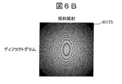
- FIG. 6A It is a figure which shows the outline of TEM whole structure provided with the spherical aberration corrector. It is a figure which shows the outline of the whole STEM structure provided with the spherical aberration corrector. It is a figure explaining formation and acquisition principle of a TEM diffractogram. It is an example of the sample used by TEM. It is an example of the TEM image at the time of vertical irradiation in TEM. It is a diffractogram of the TEM image of FIG. 5A. It is an example of the TEM image at the time of inclination irradiation in TEM. It is a diffractogram of the TEM image of FIG. 6A.
- the charged particle beam apparatus is an apparatus that accelerates particles (charged particles) having charges such as electrons and cations with an electric field and irradiates a sample.
- a charged particle beam apparatus performs observation, analysis, processing, and the like of a sample by utilizing an interaction between the sample and charged particles.
- an example applied to the STEM will be described.
- the present invention focuses on scanning a charged particle probe on the surface of an observation sample, for example, a scanning electron microscope (SEM), a focused ion beam device (FIB), Or it can apply to the apparatus which applied these by the device of a measurement sample.
- SEM scanning electron microscope
- FIB focused ion beam device
- an aberration measurement method equivalent to the diffractogram tableau method used in the aberration correction TEM can be used in the STEM by using the reciprocity of the TEM and STEM. Therefore, first, an outline of the diffractogram method in TEM will be described.
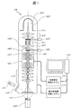
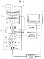
- FIG. 1 shows a schematic diagram of the overall configuration of the TEM 100.
- Each component of the TEM 100 is controlled by the electron microscope control system 117T as follows.
- the electron beam emitted from the electron source 103T at the top of the TEM mirror 101T is accelerated to an energy determined by the electron gun and the acceleration tube 102T.
- the convergence of the accelerated electron beam is adjusted by the front magnetic field of the converging lenses 104T and 107T and the objective lens 110T.
- the electron beam is deflected by the deflector 106T.
- the sample 109T held by the sample holder 108T is placed in the magnetic field of the objective lens 110T, which is a magnetic field electron lens, and the magnetic field up to the sample surface of the sample 109T is referred to as a “front magnetic field”. Is called “post-magnetic field”.
- the electron beam is guided to irradiate the observation region of the sample 109T as the irradiation electron beam 120T under conditions desired by the user such as brightness.
- the angle limit of the irradiation electron beam 120T is determined by the converging lens aperture device 105T.
- the electron beam 121T transmitted or scattered by the sample 109T is enlarged by the rear magnetic field of the objective lens 110T and the projection lens group 112T further downstream, and forms an enlarged image of the sample 109T on the fluorescent plate (projection surface) 115T.
- This image can be directly observed using the observation binoculars 113T and the like through the observation window 114T, and can further be recorded from below the projection surface by an imaging detector (CCD camera or the like) 116T or a two-dimensional imaging means such as a film.
- CCD camera CCD camera or the like
- the spherical aberration corrector 111T which has become widespread in recent years, is placed between the objective lens 110T and the projection lens group 112T in the TEM 100, and corrects on-axis aberrations up to the third order in addition to the spherical surface formed by the objective lens 110T. .
- the spherical aberration corrector 111T is controlled by the aberration correction control system 118T. This achieves a high resolution of less than 0.1 nm in the TEM100.
- FIG. 2 shows a schematic diagram of the overall configuration of the STEM 200. 2, the same components as those in FIG. 1 are denoted by the same reference numerals except “T”, and the description thereof is omitted unless particularly necessary.
- the STEM 200 includes an electron optical system that converges the electron beam emitted from the electron source 103 and scans the focused electron beam on the sample 109. Similar to the TEM, the electron beam emitted from the electron source 103 at the top of the STEM mirror 101 is guided to the electron gun and the acceleration tube 102 and the converging lenses 104 and 107 as the irradiation electron beam 120. The electron beam 120 is imaged so as to form a micro electron probe on the sample 109 by the front magnetic field of the objective lens 110.
- this micro electron probe is scanned two-dimensionally on the sample surface using a scan coil 127 (shown in FIGS. 12 and 13) disposed between the sample 109 and the aberration corrector 111. . Then, an electron beam transmitted or scattered at each point in the sample 109 is detected by an electron beam detector such as a bright field detector 126 and an annular dark field detector 125 downstream, and the intensity signal is acquired according to the raster scan. To do.
- a control device such as an electron microscope control system 117 or a control PC (Personal Computer) 119 forms an image of the sample 109 from an electron beam intensity signal from an electron beam detector. That is, the electron beam intensity signal is reconstructed into a two-dimensional image by the electron microscope control system 117 or the control PC 119. Thereby, for example, a two-dimensional image of the electron beam intensity, that is, a STEM image can be obtained on the screen of the control PC 119.
- the aberration corrector 111 is placed between the converging lens 107 and the objective lens 110, and removes the aberration in the objective lens 110 in advance (that is, cancels the aberration of the opposite sign equivalent to the objective lens aberration in advance). 111 is applied to the irradiation electron beam 120), and a finer electron probe free from blur due to aberration is imaged on the sample 109.
- the convergence angle of the irradiated electron beam on the sample surface is still limited by the converging lens aperture device 105.
- the projection lens group 112 downstream from the sample 109 is used to transmit the scattered or transmitted electron beams 121 and 122 to the detectors 125 and 126 under appropriate detection conditions.
- the imaging detector 116 is provided for aberration measurement or Ronchigram observation, but may be omitted if not required.
- FIG. 3 is a diagram for explaining a method for acquiring a diffractogram in a conventional TEM.
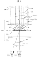
- FIG. 7 is a diagram for explaining a method for acquiring an image equivalent to a TEM diffractogram (hereinafter referred to as “STEM diffractogram”) in the STEM of this embodiment.
- STEM diffractogram TEM diffractogram
- the incident electron beam 120Ta irradiates the sample 109T in parallel with the front magnetic field 110Ta of the objective lens 110T.
- the sample 109T is a uniform amorphous thin film such as carbon, or a thin film mainly composed thereof.
- the carbon amorphous thin film has little absorption and can be regarded as a phase object with a good approximation, and since it has a random structure at the atomic level, the incident electrons are approximately isotropic. Scattered. Accordingly, a scattered electron beam 121Ta and a transmitted electron beam 122Ta that are uniform over a wide scattering angle range are generated downstream of the sample 109T. These are intermediately imaged on the intermediate image plane 150T by the back magnetic field 110Tb of the objective lens 110T. This intermediate image is further enlarged by the downstream projection lens group 112T (not shown in FIG. 3), and finally a TEM image is formed on the projection surface 115T (not shown in FIG. 3). The TEM image is observed using an imaging detector 116T or the like.
- And A ( ⁇ , z) are the electrostatic potential and vector potential of the sample, respectively.
- m, e, and h are the electron mass, charge, and Planck's constant, respectively.
- Equation 5 means taking along the electron trajectory passing through the sample and projecting it onto the exit surface. That is, the phase change of the formula 1 Can be said to directly represent the electromagnetic field information in the sample, and thus the structure.
- the electron wave function at the exit surface of the objective lens 110T is given by the Fourier transform of the equation (1). That is, It becomes.
- f 0 is the focal length of the objective lens
- F [] denotes the Fourier transform
- ⁇ ( ⁇ , ⁇ ) is an electron beam scattering angle. If the objective lens 110T and the projection lens group 112T form a complete image without lens aberration, the image can be obtained by inverse Fourier transform of the equation (8). Can be obtained.
- the objective lens 110T has an aberration, and the scattering angle is limited to a finite value. It becomes.
- a ( ⁇ ) is a transmission function determined by an objective aperture (not shown in FIG. 1)
- ⁇ ( ⁇ ) is an aberration function
- ⁇ is an electron beam wavelength.
- Equation (10) is that an extra phase change corresponding to the scattering angle is given to the electron beam due to the aberration, and as shown in FIG. 3, the ideal electron wavefront 130Ta includes an aberrational electron wavefront 130Tb. Will change. Equation (10) can be rewritten as follows based on the weak phase object approximation of the sample.
- an amorphous TEM image such as 500Ta shown in FIG. 5A is obtained on the projection surface 115T using the amorphous sample 109T shown in FIG.
- an amorphous TEM image such as 500Ta shown in FIG. 5A
- the above enhancement and suppression occur alternately as the scattering angle increases, so a ring-shaped (concentric) pattern (501Ta shown in FIG. 5B) that becomes a dark line at the scattering frequency at which the intensity is suppressed. Will get.
- An image obtained by Fourier transforming such a TEM image of an amorphous sample is called a “diffractogram”.
- the transmitted electron beam and the scattered electron beam are also correspondingly changed. It passes through another part of the objective lens 110T.
- the transmitted electron beam and the scattered electron beam are shifted at an angle ⁇ from 122Ta and 121Ta to 122Tb and 121Tb, respectively.
- a TEM image 600Tb shown in FIG. 6A is obtained.
- the frequency components included with different aberrations change while observing the same portion of the sample 109T.
- a TEM image 600Tb is obtained, and this is subjected to Fourier transform, whereby a diffractogram 601Tb shown in FIG. 6B is obtained.
- the diffractogram it is possible to know the local aberration (phase variation due to the position of the objective lens 110T through which the electron beam is transmitted), so that the diffract can be obtained at a plurality of electron beam incident angles.
- the phase variation ⁇ ( ⁇ ) due to the objective lens aberration by combining them.
- the least-order component of ⁇ ( ⁇ ) can be written as follows using the coefficients of defocus C 1 and two-fold astigmatism A 1 .
- ⁇ is a complex representation of angular space, It is. Also, Represents the conjugate complex value.
- the equation (14) By applying the equation (14) to the conditions of the equation (13) and analyzing the diffractograms 501Ta (FIG. 5B), 601Tb (FIG. 6B), etc., the defocus C 1 ( ⁇ ) and the electron beam incident angle ⁇
- the two-fold astigmatism A 1 ( ⁇ ) can be determined.
- ( ⁇ ) indicates an aberration determined at the incident angle ⁇ .
- C 1 ( ⁇ ) and A 1 ( ⁇ ) at the incident angle ⁇ are related to the axial aberration including the higher order as follows.
- This method can be extended to higher order aberration measurement in the same way. If the equation of Eq. 18 is supplemented so as to include the aberration of the desired order, the electron beam incident angle is changed as much as necessary to determine the aberration coefficient of the desired order, and the simultaneous equations of Eq.
- the axial aberration coefficient can be obtained as a solution of the linear simultaneous equations.
- the method of measuring aberrations by the above procedure is called the diffractogram tableau aberration measurement method, and is currently used as a standard method for measuring aberrations with high accuracy using the aberration correction TEM. Has been.
- FIG. 7 is a diagram for explaining an embodiment of the present invention, and is a diagram for explaining the principle that an aberration measuring method equivalent to the diffractogram tableau in the TEM explained in FIG. 3 can be applied in the STEM.
- the incident electron beam (bundle) 700 from above is converged mainly by the converging action of the front magnetic field 110a of the objective lens 110, and a micro electron probe is imaged on the sample 109.
- the micro electron probe is scanned on the sample 109 by using the scan coil (see FIGS. 12 and 13) to obtain the STEM image.
- both an electron beam transmitted through the sample 109 and an electron beam scattered by the sample 109 are taken into a detector and measured.
- the bright field detector 126a placed directly below the sample 109 and on the optical axis includes (i) an electron beam (irradiated electron beam 122a) perpendicularly incident on and transmitted through the sample 109, and (ii) a sample surface. From Incident at an angle of As a result, the scattered electron beam (irradiated electron beam 121a) vertically descending from the sample 109 reaches through the electron beam path 701a. These are signals for creating a bright field STEM image.
- the front magnetic field 110a of the objective lens 110 that contributes strongly in the formation of the STEM image as described above. If this has aberration as a lens, an extra phase variation due to the aberration is given to the electron beam when the electron beam passes, and the electron wavefront converging on the sample 109 is changed from the ideal wavefront 130a to the wavefront 130b including the variation due to the aberration. Deform. When this is applied to the bright field image observation conditions with the irradiation electron beam 122a and the irradiation electron beam 121a, each electron beam passes through a different part of the front magnetic field 110a of the objective lens 110 and thus converges on the sample 109.
- the irradiation electron beam 122a and the irradiation electron beam 121a are incident on the bright field detector 126a with different phase variations due to the aberration of the objective lens. This relationship is just the reverse of the relationship between electron beam irradiation and image formation described in TEM in FIG.
- the parallel incident electron beam is scattered by the sample 109T and passes through different positions of the back magnetic field 110Tb of the objective lens 110T together with the incident angle ⁇ of the electron beam and the scattered angle transmission electron beam.
- the phase variation due to the aberration is obtained, and an image is formed on the projection surface 115T.
- the electron beam incident in parallel is first converged by the front magnetic field 110a of the objective lens 110, it undergoes phase variation due to lens aberration.
- the electron beam scattered by the sample 109 and emitted in a specific direction is selectively detected by the bright field detector according to the position of the detector.
- an electron beam reaching one bright-field detector includes a scattered electron beam and a transmitted electron beam having a plurality of scattering angles ⁇ in the sample 109, and each of the electron beams is transmitted through an object transmitted in advance.
- Phase variation due to different lens aberrations depending on the location of the front magnetic field 110a of the lens 110 is received. Therefore, the enhancement and suppression of the electron beam intensity appear at a specific electron beam scattering angle due to the aberration of the objective lens 110, similar to that seen in the TEM.
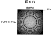
- the bright field image obtained by the bright field detector 126a obtains the STEM bright field image 900a of FIG. 9A in which a specific spatial frequency is suppressed.
- the suppressed spatial frequency can be confirmed as a dark concentric ring pattern in the image 901a of FIG. 9B obtained by Fourier transforming the STEM bright field image 900a as in TEM.
- this image 901a is an image equivalent to a diffractogram obtained by TEM, and is hereinafter referred to as a STEM diffractogram in this specification.
- the process of taking the diffractogram by changing the electron beam incident angle with TEM can be similarly performed by changing the selection of the electron beam emission angle ⁇ to be detected by changing the position of the detector.
- the transmitted electron beam incident on and transmitted through the sample 109 at the angle ⁇ when viewed with the bright field detector 126b at the position where the electron beam emitted from the sample 109 at the emission angle ⁇ in FIG. 7 is taken in, (i) the transmitted electron beam incident on and transmitted through the sample 109 at the angle ⁇ . (Irradiated electron beam 122b) and (ii) a scattered electron beam (irradiated electron beam 121b) incident on the sample 109 at an angle of ⁇ + ⁇ and turned back by ⁇ by scattering through the electron beam path 701b. It will reach the detector 126b.
- STEM bright field image 1000b (FIG. 10A) and STEM diffractogram 1001b (FIG. 10B) are obtained. Therefore, the angle of the electron beam emitted downward from the sample 109 is selected by means such as changing the position of the bright field detector.
- the axial aberration coefficient up to a desired order can be obtained even in the case of the STEM.
- FIG. 11 is a diagram in which a relationship between a sample and a detector for obtaining a bright field image used in the present invention is drawn by adding an electron beam.
- the electron beams 1101 and 1102 converged by the front magnetic field of the objective lens 110 have a half-angle cone shape and form a micro electron probe that scans the sample 109 at the tip.
- the electron beam 1111 transmitted through the sample 109 spreads at the same half angle ⁇ in the form of extending the cone of the incident electron beam below the sample 109.
- the electron beam 1112 scattered by the sample 109 is radiated into a cone inclined at a scattering angle ⁇ although it is still a half angle ⁇ .
- a scattering angle ⁇ for the sake of simplicity, only one scattered electron beam is drawn, but actually, a plurality of scatterings occur simultaneously according to the sample 109, and the cones of scattered electrons are inclined at the respective scattering angles accordingly. It will appear superimposed.
- substantially uniform scattering occurs in a wide angle range. Therefore, the cone-shaped electron beam 1112 shown in FIG. 11 is distributed almost continuously in the angular range.
- a bright field stop plate 1122 having a small hole 1121 for selection is disposed on the bright field detector 126. Is done. In the example of FIG. 11, there is a small hole 1121 in a region where the transmission electron beam and the scattered electron beam overlap on the bright field stop plate 1122, and only the transmission electron beam 1111b and the scattered electron beam 1112b that have passed therethrough are detected in the bright field. Reach vessel 126.
- the hole diameter of the small hole 1121 is determined according to the size of the structure to be observed. If the representative length of the sample structure to be observed is d, the half-angle ⁇ for viewing the small hole 1121 from the sample 109 is It becomes.
- ⁇ is the electron beam wavelength
- C s is the spherical aberration coefficient of the objective lens (110a in FIG. 7) in the optical system that performs aberration measurement.
- the hole diameter must be limited so that If the distance from the sample 109 to the bright field stop plate 1122, that is, the so-called camera length L, is 200 mm, the small hole diameter is 1.7 mm.
- the bright field detector 126 main body that detects the electron beam that has passed through the small hole 1121 of the bright field stop plate 1122 is a scintillator, a semiconductor detector, or the like for detecting electrons.
- the electron intensity signal detected by the bright field detector 126 is subjected to preprocessing such as amplification by the preamplifier 128 and is sent to the control PC 119.
- the control PC 119 performs STEM image formation and diffractogram calculation processing.
- the control PC 119 creates a plurality of images (FIG. 9B and FIG. 10B) by Fourier transforming each of the plurality of images acquired at a plurality of transmission angles with respect to the sample 109, and uses the plurality of images to transmit a plurality of transmissions.
- control PC119 obtains the aberration coefficients based on the defocus C 1 for each of a plurality of transmission angle (tau) and dyad symmetry astigmatism A 1 ( ⁇ ).
- the control PC 119 is a general-purpose computer.
- the process of the control PC 119 may be realized as a function of a program executed on the computer. That is, the process of the control PC 119 may be realized by storing a program code in a storage unit such as a memory and executing a program code by a processor such as a CPU (Central Processing Unit).
- a processor such as a CPU (Central Processing Unit).
- FIG. 12 is a diagram showing the configuration of an embodiment of the present invention.
- a configuration example using a bright field detector array 1260 in which a plurality of bright field detectors 126a, 126b, and 126c are arranged in an array is shown.
- FIG. 12 shows a portion below the aberration corrector 111 of FIG. 2 for explaining the general structure of the STEM.
- the incident electron beam bundle 1200 is given a negative spherical aberration that cancels out the spherical aberration of the objective lens 110 in advance by the aberration corrector 111, and the micro electron probe is converged on the sample 109 by the front magnetic field of the objective lens 110.
- the electrons transmitted or scattered through the sample 109 are appropriately adjusted in magnification / camera length by the projection lens 112 and are incident on the lowermost bright field detector array 1260.
- FIG. 12 shows a bright field detector array 1260 including three bright field detectors 126a, 126b, and 126c.
- bright field images must be acquired at a plurality of emission angles corresponding to the number of aberrations to be measured.
- projection is performed so that the emission angle from the sample 109 to each bright field detector 126a, 126b, and 126c is appropriate.
- the lens 112 is adjusted.
- each of the bright field detectors 126a, 126b, and 126c can obtain an electron intensity signal at a different emission angle.
- reference numerals 1201 a, 1201 b, and 1201 c in FIG. 12 indicate three transmission and scattered electron beam paths emitted from the sample 109.
- Signals obtained by the bright field detectors 126a, 126b, and 126c are amplified by the preamplifiers 128a, 128b, and 128c, and sent to the control PC 119.
- the control PC 119 can simultaneously obtain a bright field image, and thus a diffractogram, from the signals obtained by the bright field detectors 126a, 126b, and 126c.
- FIG. 12 only three detectors are shown for the sake of simplification, but if nine or more detectors are arranged two-dimensionally, the fifth-order or lower axial aberration can be calculated. . That is, according to the embodiment shown in FIG. 12, a plurality of electron beam incidence conditions can be changed while the electron beam incidence conditions are changed, such as the diffractogram tableau method in the original TEM and the probe measurement method conventionally used in the STEM. There is no need to repeat the measurement. Further, the extraction of aberration information from the obtained STEM image and the calculation of the on-axis aberration can be performed with high accuracy by the same method as the diffractogram tableau method in TEM that has been sufficiently confirmed so far.
- FIG. 13 is a diagram showing the configuration of another embodiment of the present invention.
- this embodiment includes one bright field detector 126 and an electron beam deflector 129 for guiding the transmitted or scattered electron beam to the bright field detector 126 for selection.
- the electron beam deflector 129 sequentially selects electron beams having different emission angles, and acquires STEM images for the different emission angles.
- FIG. 13 for the sake of simplicity, three transmitted and scattered electron beams (electron beam paths) 1201a, 1201b, and 1201c emitted from the sample 109 are shown.
- the electron beam deflector 129 is used first.
- One transmitted and scattered electron beam 1201a is guided to the bright field detector 126, and an STEM image corresponding to the emission angle is obtained.
- the electron beam is shaken again so that the second transmitted and scattered electron beam 1201b is again guided to the bright field detector 126, and an STEM image is acquired.
- STEM images are acquired in the same manner for the third transmitted and scattered electron beam 1201c.
- the transmitted and scattered electron beams 1201a, 1201b, and 1201c detected by the electron beam deflector 129 are sequentially selected, and a necessary number of STEM images are acquired. After acquiring the STEM image, the axial aberration coefficient is calculated by the method described above.
- the electron beam to be detected can be selected by adjusting only the electron beam deflector 129 directly above the bright field detector 126 without adjusting the electron optical element such as a detector. That is, it is possible to adjust only the electron beam deflector 129 directly above the bright field detector 126 and acquire a STEM image necessary for measurement.
- the incident electron beam is transmitted using at least two stages of deflectors that place a TEM image or STEM image necessary for measurement above the corrector.
- the electron beam incident angle with respect to the sample must be adjusted with accurate parallel displacement. Therefore, according to the embodiment shown in FIGS. 12 and 13, it is easy to extract aberration information as compared with the existing aberration measurement method, and it is possible to provide an aberration measurement method with high measurement accuracy.
- FIGS. 14A to 14C show examples of the bright field detector array 1260 used in the example of FIG.
- the bright field detector array 1260 used in the aberration measurement method of this embodiment includes the electron detector body and the limit of the electron beam angle to be detected according to the condition of the equation (20). And a diaphragm for carrying out above.
- each of the single hole apertures 1402a, 1402b, 1402c,... Has a hole for limiting the electron beam to an emission angle that is a detection target. Note that the diaphragm need only be capable of limiting the emission angle of the electron beam that is appropriately detected by each of the electron detectors 1401a, 1401b, 1401c,. .
- the bright field detector array 1260B of FIG. 14B includes a plurality of electron detectors 1401a, 1401b, 1401c,..., And a single diaphragm plate 1402.
- the diaphragm plate 1402 has a porous array corresponding to the detector array. Therefore, the bright field detector array 1260B can be configured by inserting the diaphragm plate 1402 on the plurality of electron detectors 1401a, 1401b, 1401c,.
- the diaphragm plate 1402 may be of a mechanism that is inserted later onto the detector array independently of the electron detectors 1401a, 1401b, 1401c,.
- the bright field detector array 1260C of FIG. 14C includes a diaphragm plate 1402, a conversion element 1404, and a two-dimensional imaging sensor 1405.
- a two-dimensional imaging sensor 1405 such as a CCD may be substituted for the detector side.
- an electron beam that has passed through a diaphragm plate 1402 having a porous array of an appropriate arrangement is guided to a two-dimensional imaging sensor 1405 through a conversion element 1404 (in the case of a CCD, from an electron such as a fluorescent plate or a scintillator to light). Conversion element 1404 is used).
- a signal of the pixel of the two-dimensional imaging sensor 1405 corresponding to each hole of the diaphragm plate 1402 is taken out, and a scanning image (STEM image) may be reproduced for each electron beam.
- STEM image scanning image
- FIGS. 15A to 15B show examples of arrangements of electron detectors and apertures in a bright field detector array.
- the number of bright-field detectors may be sufficient to satisfy the simultaneous equations (Equation 18) sufficient to calculate the desired axial aberration coefficient, and the arrangement also calculates the desired axial aberration coefficient. It suffices if it is at a position where an appropriate emission angle can be selected. Note that the selection of the emission angle can also be adjusted as appropriate with the projection lens 112 shown in FIGS.
- an axial aberration coefficient can be obtained in principle.
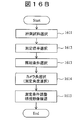
- FIG. 16A is a flowchart of an aberration corrector adjustment operation using the aberration measurement method according to one embodiment of the present invention.
- the lens excitation and deflector optical conditions that can be determined by prior experiments and simulations are set as preset conditions (1601).
- step 1602 adjustment for obtaining a bright field image is performed (1602).
- the contents of step 1602 will be described with reference to FIG. 16B.
- a measurement sample is selected and a measurement location in the sample is selected (1611).
- STEM magnification and irradiation conditions suitable for aberration measurement are set (1612, 1613). The magnification is appropriately adjusted according to the magnitude of the remaining aberration.
- the effective camera length from the sample 109 to the bright field detector is adjusted by adjusting the projection lens 112 (1614). In this operation, particularly when the bright field detector array 1260 is used, the camera length is set so that an electron beam having an appropriate emission angle reaches each detector of the array.
- respective setting values and STEM images are displayed on the monitor of the control PC 119 (1615).
- the operator can adjust various setting conditions via the user interface.
- the STEM diffractogram is acquired (1603).
- the contents of step 1603 will be described with reference to FIG. 16C.
- this process will be described using the bright field detector array 1260 of FIG.
- the bright field detector array 1260 is activated (1621).
- a diaphragm such as a diaphragm plate 1402 in FIG. 14B
- an imaging operation two-dimensional scanning on the sample surface with an electronic probe
- STEM images in the electron beam emission azimuth from the sample 109 corresponding to the respective detectors can be obtained from the signals obtained by the respective detectors of the bright field detector array 1260. This satisfies the requirement based on the measurement principle described in FIG. If each STEM image obtained here is Fourier-transformed (1624) and matched with the electron beam emission angle from the sample 109, the STEM diffractogram table can be obtained (1625).
- the STEM diffractogram table means a table in which the electron beam emission angle from the sample 109 is associated with the STEM diffractogram.
- the control PC 119 calculates an axial aberration coefficient using the STEM diffractogram table obtained in step 1603 (1604). This step is almost the same as the procedure for calculating the on-axis aberration coefficient from the diffractogram tableau in the TEM as described above. Details will be described with reference to FIG. 16D. First, a defocus C 1 ( ⁇ i ) and a two-fold symmetric astigmatism A 1 ( ⁇ i ) with respect to the output angle ⁇ i corresponding to the i-th among a plurality of obtained diffractograms are extracted (1631).
- a multiple simultaneous equation is created from the relational expression of C 1 ( ⁇ i ) and A 1 ( ⁇ i ) and the axial aberration coefficient shown in the equation (18), and means such as the least square method is used.
- the axial aberration coefficient is derived (1632).
- the axial aberration count to be corrected is output (1633), and displayed on the monitor of the control PC 119 by graphical means such as an aberration coefficient, aberration figure, or wavefront aberration (1634).
- the operator can confirm the information displayed on the monitor.
- the STEM diffractogram table is also displayed on the monitor at the same time (1635). Displaying the STEM diffractogram table is useful for grasping the aberration state, and allows the operator to confirm the appropriateness of the aberration measurement regarding what diffractogram was acquired and the aberration measurement was performed. So desirable.
- the control PC 119 determines the correction state from the aberration coefficient obtained through a series of aberration measurements (1605). If the measured value of the aberration coefficient to be corrected is equal to or less than a separately determined tolerance, this aberration adjustment is complete. On the other hand, if the aberration coefficient deviates from the allowable value, residual aberration compensation adjustment is performed to reduce the aberration (1606). Then, in order to confirm whether or not the aberration is sufficiently reduced by the correction performed according to the compensation adjustment, and whether or not another aberration is increased parasitically at the time of tuning, the process returns to step 1602. Repeat the aberration measurement. As the aberration correction progresses and the residual aberration decreases, the appropriate image magnification and camera length also change, so it is better to adjust them appropriately.
- step 1605 After obtaining a diffractogram (1603) and calculating an aberration coefficient (1604), it is determined in step 1605 that all the aberration coefficients to be compensated are equal to or less than an allowable value and the aberration correction adjustment is completed. Until this, the aberration measurement and compensation adjustment steps as described above are repeated. As described above, the aberration states of the STEM aberration corrector 111 and the objective lens 110 can be evaluated.
- aberration measurement is important for evaluating the state of the charged particle optical system.
- a highly accurate aberration (coefficient) measurement technique has been required more than ever before for adjustment of the aberration corrector and evaluation of the aberration correction state.
- these aberration measurement methods there are known an aberration graphic method and a probe tableau method for acquiring aberration-induced displacement and image distortion by changing a plurality of incident conditions of a charged particle beam to a lens to be measured, and deriving an aberration coefficient.
- the measurement procedure is complicated and the measurement time is long. This made it difficult to adjust the aberration corrector itself, which requires repeated measurement.
- STEM aberration measurement an image (STEM diffractogram) equivalent to a diffractogram using the reciprocity of STEM and TEM is acquired, and an axial aberration coefficient is calculated using this. This avoids complex image analysis for aberration information extraction found in the Ronchigram method.
- a bright field detector array 1260 in which a plurality of STEM bright field detectors are arranged, or a detector equivalent thereto is used. Accordingly, STEM images for a plurality of incident angles can be obtained simultaneously in parallel, and a STEM diffractogram for each incident angle can be calculated. Therefore, information equivalent to the diffractogram can be acquired collectively without repeating a plurality of measurements. In other words, the aberration measurement can be completed in a short time in a single measurement. Therefore, the complexity of measurement can be greatly reduced.
- a plurality of transmission and scattering electron beams having different angles are sequentially selected by the electron beam deflector 129, and the transmission and scattered electron beams are detected by one STEM bright field detector 126.
- this configuration it is possible to adjust only the electron beam deflector 129 directly above the bright field detector 126 and obtain a STEM image necessary for measurement.
- This configuration is simpler than the conventional aberration measurement using the diffractogram tableau method with the TEM or the probe tableau method with the STEM, and the complexity of the measurement can be reduced.
- this invention is not limited to the Example mentioned above, Various modifications are included.
- the above-described embodiments have been described in detail for easy understanding of the present invention, and are not necessarily limited to those having all the configurations described.
- a part of the configuration of one embodiment may be replaced with the configuration of another embodiment, and the configuration of another embodiment may be added to the configuration of one embodiment.
- control devices such as the aberration correction control system (118T, 118), the electron microscope control system (117T, 117), and the control PC (119T, 119) of the embodiment are partly or entirely designed by, for example, an integrated circuit. This may be realized by hardware.
- the functions of the control device described above may be realized by software program codes.
- a non-transitory computer readable medium non-transitory computer readable medium in which the program code is recorded is provided to the information processing device (computer), and the information processing device (or CPU) is a non-transitory computer readable medium.
- the program code stored in is read.
- non-transitory computer-readable medium for example, a flexible disk, a CD-ROM, a DVD-ROM, a hard disk, an optical disk, a magneto-optical disk, a CD-R, a magnetic tape, a nonvolatile memory card, a ROM, and the like are used.
- the program code may be supplied to the information processing apparatus by various types of temporary computer-readable media.
- Examples of transitory computer readable media include electrical signals, optical signals, and electromagnetic waves.
- the temporary computer-readable medium can supply the program to the information processing apparatus via a wired communication path such as an electric wire and an optical fiber, or a wireless communication path.
- control lines and information lines in the drawings indicate what is considered necessary for the explanation, and not all control lines and information lines on the product are necessarily shown. All the components may be connected to each other.
- TEM 200 STEM 101, 101T: Mirror body 102, 102T: Electron gun and acceleration tube 103, 103T: Electron source 104, 104T: Converging lens 105, 105T: Converging lens diaphragm 106, 106T: Deflectors 107, 107T: Converging lenses 108, 108T : Sample holder 109, 109T: Sample 110, 110T: Objective lens 110a, 110Ta: Objective lens pre-magnetic field 110b, 110Tb: Objective lens post-magnetic field 111, 111T: Aberration corrector 112, 112T: Projection lens 113T: Observation binoculars 114T: Observation window 115T: Projection surface (fluorescent screen) 116, 116T: Imaging detector (CCD camera, etc.) 117, 117T: Electron microscope control system 118, 118T: Aberration correction control system 119, 119T: Control PC 120, 120T: irradiation electron
Abstract
Provided is a charged particle beam device with which the extraction of aberration information is easy compared to existing aberration measurement methods, and which can perform highly-accurate aberration measurement. The charged particle beam device comprises the following: an electron optical system that scans converged charged particle beams on a sample (109); detection systems (126a, 126b) that detect charged particle beams which have passed through, or scattered off of, the sample (109); an aberration correction device that corrects aberration of the electron optical system; and a control device that forms an image of the sample (109) from signals from the detection systems (126a, 126b). The charged particle beam device, wherein a plurality of images are formed by carrying out Fourier transform on each of the plurality of images of the sample (109) acquired at a plurality of detection angles, and aberration information is found for each of the plurality of detection angles by using the plurality of images.
Description
本発明は、荷電粒子線装置、及び、当該荷電粒子線装置において光学状態(収差)を求めるための方法に関するものである。
The present invention relates to a charged particle beam apparatus and a method for obtaining an optical state (aberration) in the charged particle beam apparatus.
近年、走査透過電子顕微鏡(STEM)、透過電子顕微鏡(TEM)における球面収差補正技術が実用化され、それ以前には電子レンズの大きな球面収差に隠れてあまり重視されなかった微小な種々の収差の影響を適切に取り扱う方法が重要となってきている。
In recent years, spherical aberration correction technology in a scanning transmission electron microscope (STEM) and a transmission electron microscope (TEM) has been put into practical use. How to deal with the effects appropriately is becoming important.
例えば、STEMにおいて問題となる三次以下の収差については、従来、デフォーカス、二回対称非点とせいぜい三回対称非点の3収差について評価及び補償の対策を講じれば良かった。しかしながら、球面収差補正器が実用化されて以降、球面収差を補正した後に残る前記以外の軸上コマ収差、スター収差、四回対称非点収差、球面収差自体を含め計7収差を適切に取り扱うことが必要となった。さらに、最高分解能を得るためには、より高次(2012年現在で一般的には5次以下)の14個の軸上開口収差を評価し、調整または抑制する工夫が必要であることが分かっている。
For example, for third-order and lower aberrations that are problematic in STEM, conventionally, it has only been necessary to take measures for evaluation and compensation for three aberrations of defocus, two-fold symmetric astigmatism and at most three-fold symmetric astigmatism. However, since the spherical aberration corrector has been put into practical use, a total of seven aberrations, including on-axis coma, star aberration, four-fold astigmatism, and spherical aberration itself, remaining after correction of spherical aberration are properly handled. It became necessary. Furthermore, in order to obtain the highest resolution, it is found that 14 higher-order (generally 5th order or less as of 2012) 14 axial aperture aberrations must be evaluated and adjusted or suppressed. ing.

これより明らかなように、各レンズ収差の評価、即ち収差係数の精密測定法は、電子顕微鏡の収差補正技術の確立以前とは桁違いに重要さを増している。収差補正STEMにおいては、従来より、プローブタブロー法(非特許文献1)や収差図形法、あるいはロンチグラムを用いる収差測定法(特許文献1及び特許文献2)が実用化されている。前述したもののうち前二者は、試料面上に入射する電子線の入射角度を変えながら走査顕微鏡像を撮影し、それぞれの角度で得られる収差情報を纏め、表1に示す14種の軸上収差を計算する手法である。
As is clear from the above, the evaluation of each lens aberration, that is, the precise measurement method of the aberration coefficient, has become much more important than before the establishment of the electron microscope aberration correction technology. Conventionally, in the aberration correction STEM, a probe tableau method (Non-patent Document 1), an aberration graphic method, or an aberration measurement method using Ronchigram (Patent Document 1 and Patent Document 2) has been put into practical use. Among the above-mentioned, the former two take a scanning microscope image while changing the incident angle of the electron beam incident on the sample surface, summarize the aberration information obtained at each angle, and have 14 types of on-axis shown in Table 1. This is a method for calculating aberrations.
具体的には、プローブタブロー法では、入射角度毎のプローブ形状を推定し、当該入射電子線傾斜での二回対称非点収差とでデフォーカスを算出する。これを当該傾斜角度における収差情報として軸上収差係数を計算する。また、収差図形法では、各入射電子線傾斜の走査顕微鏡像のシフト量を調べ、これらを当該傾斜角度における収差情報として軸上収差係数を算出する。
Specifically, in the probe tableau method, the probe shape for each incident angle is estimated, and the defocus is calculated with the two-fold astigmatism at the incident electron beam inclination. The axial aberration coefficient is calculated using this as aberration information at the tilt angle. In the aberration graphic method, the shift amount of the scanning microscope image of each incident electron beam tilt is examined, and the axial aberration coefficient is calculated using these as aberration information at the tilt angle.
表1の回転対称収差以外は、収差の大きさと共に回転角というあわせて二つの自由度を有するので、次数が3次以下で7つの収差係数を決定するには12個、次数が5次以下で14個の収差係数を決定するには25個の不定値を求めなければならない。この数は即ち必要とする最低測定条件の数(上記の2つの方法であれば、電子線の入射角度の選択数)に相当する。
In addition to the rotationally symmetric aberrations in Table 1, there are two degrees of freedom, ie, the rotation angle as well as the magnitude of the aberration. Therefore, 12 orders are used for determining the seven aberration coefficients with the order of 3 or less, and the order is 5 or less. In order to determine 14 aberration coefficients, 25 indefinite values must be obtained. This number corresponds to the number of minimum measurement conditions required (in the case of the above two methods, the number of incident angles of electron beams selected).
さらに、測定の統計的誤差あるいは系統的誤差を補償するために、通常は、必要数より余分な数の測定を繰り返す必要がある。即ち、これらの手法は、上記の通り必要とする収差係数を求めるためにその数に応じた多数の測定を、電子線入射角度等の条件を変えながら繰り返し行わなければならない。したがって、測定の手順が煩雑となる上、測定中の装置、あるいは被測定試料の不安定性が収差測定精度に影響し、その誤差が大きくなるという課題がある。
Furthermore, in order to compensate for statistical or systematic errors in measurement, it is usually necessary to repeat an extra number of measurements than necessary. That is, in these methods, in order to obtain the required aberration coefficient as described above, a number of measurements corresponding to the number must be repeated while changing conditions such as the electron beam incident angle. Therefore, there is a problem that the measurement procedure becomes complicated, and the instability of the apparatus under measurement or the sample to be measured affects the aberration measurement accuracy, and the error becomes large.
一方、ロンチグラムを用いる方法(例えば、特許文献1)では、同様に複数の収差に起因する像のシフト、あるいはデフォーカスと非点収差等を複数の電子線入射角度に対して抽出して、必要となる軸上収差係数の組を算出する。ただし、特許文献1で説明される通り、これら複数の電子線入射角度に対する情報は、一枚のロンチグラムに集約されて表される。そのため、前述のプローブタブロー法のように繁雑に多数の測定を繰り返すことなく、比較的少数の測定(ロンチグラムの撮影)で必要な情報を得て、軸上収差係数の組を算出することができる。
On the other hand, in the method using Ronchigram (for example, Patent Document 1), it is necessary to extract image shift caused by a plurality of aberrations, or defocus and astigmatism for a plurality of electron beam incident angles. A set of on-axis aberration coefficients is calculated. However, as described in Patent Document 1, information on the plurality of electron beam incident angles is expressed in a single Ronchigram. Therefore, a set of axial aberration coefficients can be calculated by obtaining necessary information with a relatively small number of measurements (shooting Ronchigrams) without repeating many measurements as in the probe table method described above. .
実際には、測定手順の要請からロンチグラム一枚のみでは不十分であり、例えば、特許文献1においては、デフォーカスを変えた最低二枚のロンチグラムが収差係数の算出に必要としている。また、統計的に測定精度を上げる目的で、複数枚のロンチグラムを撮影する場合もある。しかしながら、プローブタブロー法と比較して格段に少ない測定数で、必要な軸上収差係数の組を求めることができるのがロンチグラム法の利点である。
Actually, only one Ronchigram is insufficient because of the request for the measurement procedure. For example, in Patent Document 1, at least two Ronchigrams with different defocus are required for calculating the aberration coefficient. In addition, a plurality of Ronchigrams may be taken for the purpose of statistically increasing the measurement accuracy. However, it is an advantage of the Ronchigram method that a set of necessary on-axis aberration coefficients can be obtained with a significantly smaller number of measurements compared to the probe tableau method.
一方、上記の通り、一枚のロンチグラム中には多数の電子線入射角度に相当する収差情報が含まれることから、ロンチグラムからそれぞれの情報を抽出する画像解析に工夫と注意を要する。例えば、特許文献1では、測定試料としてアモルファス薄膜を用いる。この測定試料から得られたロンチグラム内で被測定領域をさらに格子状に区分けして、各々の領域で軸上収差算出に必要な収差情報を取得する。ここで、区分けされた各格子は、前述のプローブタブロー法等による異なる入射角度での観察に相当する。また、ロンチグラムから抽出する収差情報とは、その区画内の平均的な像歪みに関する特徴量である。この像歪みに関する特徴量は、その区画に対応する入射角度での電子プローブの変形、或いは局所倍率の変化と関係付けられる。
On the other hand, as described above, since one piece of Ronchigram includes aberration information corresponding to a large number of electron beam incident angles, it is necessary to devise and pay attention to image analysis for extracting each piece of information from the Ronchigram. For example, in Patent Document 1, an amorphous thin film is used as a measurement sample. Within the Ronchigram obtained from this measurement sample, the region to be measured is further divided into a lattice shape, and aberration information necessary for calculating the on-axis aberration is obtained in each region. Here, each of the divided gratings corresponds to observation at different incident angles by the above-described probe tableau method or the like. In addition, the aberration information extracted from the Ronchigram is a feature amount related to the average image distortion in the section. The feature amount related to the image distortion is related to the deformation of the electron probe at the incident angle corresponding to the section or the change of the local magnification.
この一連の画像解析において正しい収差測定を得るためには、格子の大きさを適正に設定することが必要である。格子が小さすぎればその領域を代表する収差情報を十分な精度で取得できない。一方、格子が広すぎれば領域内で平均化されてしまって、やはり正しい収差情報が取得できず、その結果、収差測定結果に応分の誤差を生じることになる。
In order to obtain correct aberration measurement in this series of image analysis, it is necessary to set the size of the grating appropriately. If the grating is too small, the aberration information representing the area cannot be acquired with sufficient accuracy. On the other hand, if the grating is too wide, it is averaged within the region, and correct aberration information cannot be obtained, resulting in a corresponding error in the aberration measurement result.
また、測定試料固有の形状や試料ドリフト、電気的あるいは機械的ノイズ等、収差以外の要因もロンチグラムに影響を及ぼすので、これらによっても取得される収差情報、引いてはそれらより算出される軸上収差係数に誤差が生じる可能性がある。まとめれば、ロンチグラムによる収差測定では、元々の収差状態に応じて適切な測定条件を正しく選択し、且つ、ロンチグラムからの収差情報抽出も収差以外の影響を考慮した画像処理方法に工夫する必要があると言える。
In addition, factors other than aberration, such as the shape unique to the measurement sample, sample drift, electrical or mechanical noise, etc., also affect the Ronchigram. An error may occur in the aberration coefficient. In summary, in the aberration measurement by Ronchigram, it is necessary to properly select an appropriate measurement condition according to the original aberration state, and to devise an image processing method that considers influences other than aberration in extracting aberration information from Ronchigram. It can be said.
他方、収差補正透過電子顕微鏡(TEM)においても幾つかの精密収差測定法が考案されている。今のところ、実用的にはディフラクトグラムタブローを用いる測定法(非特許文献2)が主流である。この測定法の詳細については、本発明との比較において後述するが、ディフラクトグラムタブロー法もSTEMプローブタブロー法と同様に、試料に対して複数の電子線入射角度で測定し、各々の入射角度で得られるTEM像におけるデフォーカスと非点収差を求め、これらから軸上収差係数を算出する。その意味では、ディフラクトグラムタブロー法は、STEMプローブタブロー法と同様に、多数回の測定を繰り返す必要があり、測定手順の煩雑さと測定時間に課題があると言える。
On the other hand, several precision aberration measurement methods have been devised in the aberration-corrected transmission electron microscope (TEM). At present, the measurement method using a diffractogram tableau (Non-Patent Document 2) is the mainstream in practical use. Details of this measurement method will be described later in comparison with the present invention, but the diffractogram tableau method is also measured at a plurality of electron beam incident angles with respect to the sample in the same manner as the STEM probe tableau method. The defocus and astigmatism in the TEM image obtained in the above are obtained, and the axial aberration coefficient is calculated therefrom. In that sense, like the STEM probe tableau method, the diffractogram tableau method needs to be repeated many times, and it can be said that there are problems in the complexity of the measurement procedure and the measurement time.
一方、各々のディフラクトグラムからの収差情報の抽出は、前述のSTEMにおける各測定法のそれらに比べても単純である。そのため、ある程度像質の良いディフラクトグラムが得られれば、その抽出は比較的容易かつ精度も維持できる。従って、収差情報抽出に起因する収差測定誤差は小さく抑えられると期待できるが、一方、勿論ながらディフラクトグラムタブローはTEMにおける収差測定法であり、そのままではSTEMにおいて適用することはできない。
On the other hand, the extraction of aberration information from each diffractogram is simpler than that of each measurement method in the STEM described above. Therefore, if a diffractogram with a certain level of image quality is obtained, the extraction can be performed relatively easily and with high accuracy. Therefore, it can be expected that the aberration measurement error caused by the aberration information extraction can be suppressed to a small level. On the other hand, of course, the diffractogram tableau is an aberration measurement method in the TEM and cannot be applied in the STEM as it is.
上記既存技術で説明した通り、STEMにおける既存の収差測定法は、多数回の測定を要する煩雑な方法であるか、あるいは、測定回数は少ないが収差情報抽出の工程で誤差を含み易い。したがって、既存の収差測定法ではまだ課題を残していると言える。実際、現状の収差補正STEMにおいては、複数回の収差測定と収差調整を繰り返すことによって漸近的に所望の収差補正状態に近づけていく作業を行う。これは、収差調整の不完全性もあるが、同時に上記で課題とした収差測定の精度及び確度の不足も原因となっている。
As described in the above-mentioned existing technology, the existing aberration measurement method in the STEM is a complicated method that requires a large number of measurements, or the number of times of measurement is small, but errors are easily included in the aberration information extraction process. Therefore, it can be said that the existing aberration measurement method still has a problem. Actually, in the current aberration correction STEM, an operation of asymptotically approaching a desired aberration correction state is performed by repeating aberration measurement and aberration adjustment a plurality of times. This is due to imperfections in aberration adjustment, but at the same time, it is also caused by the lack of accuracy and accuracy of aberration measurement, which is the problem described above.
本発明の目的は、既存の収差測定法に比べて収差情報の抽出が容易であり、測定精度の高い収差測定を行うことが可能な荷電粒子線装置及び収差測定法を提供することにある。
An object of the present invention is to provide a charged particle beam apparatus and an aberration measurement method that can easily extract aberration information and can perform aberration measurement with high measurement accuracy as compared with existing aberration measurement methods.
上記課題を解決するために、例えば請求の範囲に記載の構成を採用する。本願は上記課題を解決する手段を複数含んでいるが、その一例として、荷電粒子源から放出された荷電粒子線を収束して、前記収束された荷電粒子線を試料上で走査させる電子光学系と、前記試料から透過あるいは散乱した荷電粒子線を検出する検出系と、前記電子光学系の収差を補正する収差補正器と、前記検出系からの信号から前記試料の画像を形成する制御装置と、を備え、前記制御装置は、前記試料に対して複数の検出角度で取得した複数の画像を各々フーリエ変換することにより複数の像を作成し、前記複数の像を用いて前記複数の検出角度の各々に対する収差情報を求める、荷電粒子線装置が提供される。
In order to solve the above problems, for example, the configuration described in the claims is adopted. The present application includes a plurality of means for solving the above problems. As an example, an electron optical system that converges a charged particle beam emitted from a charged particle source and scans the converged charged particle beam on a sample. A detection system that detects a charged particle beam transmitted or scattered from the sample, an aberration corrector that corrects aberrations of the electron optical system, and a control device that forms an image of the sample from a signal from the detection system; The control device creates a plurality of images by Fourier transforming each of a plurality of images acquired at a plurality of detection angles with respect to the sample, and uses the plurality of images to generate the plurality of detection angles. A charged particle beam device is provided for determining aberration information for each of the above.
他の例によれば、荷電粒子線装置における収差測定法であって、荷電粒子源から放出された荷電粒子線を収束して、前記収束された荷電粒子線を試料上で走査させる照射ステップと、前記試料から透過あるいは散乱した荷電粒子線を検出する検出ステップと、前記検出ステップで得られた信号から前記試料の画像を形成する画像形成ステップと、前記試料に対して複数の検出角度で取得した複数の画像を各々フーリエ変換することにより複数の像を作成する像作成ステップと、前記複数の像を用いて前記複数の検出角度の各々に対する収差情報を求める収差情報算出ステップと、を含む収差測定法が提供される。
According to another example, an aberration measurement method in a charged particle beam apparatus, the irradiation step of converging a charged particle beam emitted from a charged particle source and scanning the focused charged particle beam on a sample; A detection step of detecting a charged particle beam transmitted or scattered from the sample, an image formation step of forming an image of the sample from a signal obtained in the detection step, and acquisition at a plurality of detection angles with respect to the sample An aberration including: an image creation step of creating a plurality of images by Fourier transforming each of the plurality of images; and an aberration information calculation step of obtaining aberration information for each of the plurality of detection angles using the plurality of images. A measurement method is provided.
本発明によれば、既存の収差測定法に比べて収差情報抽出が容易であり、測定精度の高い荷電粒子線装置及び収差測定方法を提供することができる。
本発明に関連する更なる特徴は、本明細書の記述、添付図面から明らかになるものである。また、上記した以外の、課題、構成及び効果は、以下の実施例の説明により明らかにされる。 According to the present invention, it is possible to provide a charged particle beam apparatus and an aberration measurement method that can easily extract aberration information and have high measurement accuracy as compared with existing aberration measurement methods.
Further features related to the present invention will become apparent from the description of the present specification and the accompanying drawings. Further, problems, configurations and effects other than those described above will be clarified by the description of the following examples.
以下、添付図面を参照して本発明の実施例について説明する。なお、添付図面は本発明の原理に則った具体的な実施例を示しているが、これらは本発明の理解のためのものであり、決して本発明を限定的に解釈するために用いられるものではない。
Hereinafter, embodiments of the present invention will be described with reference to the accompanying drawings. The accompanying drawings show specific embodiments in accordance with the principle of the present invention, but these are for the understanding of the present invention, and are never used to interpret the present invention in a limited manner. is not.
荷電粒子線装置は、電子や陽イオンなどの電荷をもつ粒子(荷電粒子)を電界で加速し、試料に照射する装置である。荷電粒子線装置は、試料と荷電粒子との相互作用を利用して、試料の観察、分析、加工などを行う。以下の説明ではSTEMに適用した例を説明するが、本発明は、観察試料表面に荷電粒子プローブを収束して走査するもの、例えば、走査電子顕微鏡(SEM)、集束イオンビーム装置(FIB)、またはこれらを応用した装置にも、測定試料の工夫等で適用可能である。
The charged particle beam apparatus is an apparatus that accelerates particles (charged particles) having charges such as electrons and cations with an electric field and irradiates a sample. A charged particle beam apparatus performs observation, analysis, processing, and the like of a sample by utilizing an interaction between the sample and charged particles. In the following description, an example applied to the STEM will be described. However, the present invention focuses on scanning a charged particle probe on the surface of an observation sample, for example, a scanning electron microscope (SEM), a focused ion beam device (FIB), Or it can apply to the apparatus which applied these by the device of a measurement sample.
以下で説明する実施例は、収差補正TEMで用いられているディフラクトグラムタブロー法と同等の収差測定法を、TEMとSTEMの相反性を用いて、STEMでも利用可能とするものである。そのため、まずTEMにおけるディフラクトグラム法の概略について説明する。
In the embodiment described below, an aberration measurement method equivalent to the diffractogram tableau method used in the aberration correction TEM can be used in the STEM by using the reciprocity of the TEM and STEM. Therefore, first, an outline of the diffractogram method in TEM will be described.
図1は、TEM100の全体構成の概略図を示す。TEM100の各構成要素は、電子顕微鏡制御システム117Tによって以下のように制御される。TEM鏡体101Tの頭頂部にある電子源103Tから放射された電子線は、電子銃および加速管102Tで決められたエネルギーまで加速される。加速された電子線は、収束レンズ104T、107Tと対物レンズ110Tの前磁場で収束が調整される。また、電子線は、偏向器106Tで偏向される。ここで、試料ホルダ108Tで保持された試料109Tは、磁界電子レンズである対物レンズ110Tの磁場中に置かれ、試料109Tの試料面までの磁場を「前磁場」と呼び、試料面以降の磁場を「後磁場」と呼ぶ。以上により、電子線は、照射電子線120Tとして試料109Tの観察領域を明るさなどユーザ所望の条件で照射するように導かれる。
FIG. 1 shows a schematic diagram of the overall configuration of the TEM 100. Each component of the TEM 100 is controlled by the electron microscope control system 117T as follows. The electron beam emitted from the electron source 103T at the top of the TEM mirror 101T is accelerated to an energy determined by the electron gun and the acceleration tube 102T. The convergence of the accelerated electron beam is adjusted by the front magnetic field of the converging lenses 104T and 107T and the objective lens 110T. The electron beam is deflected by the deflector 106T. Here, the sample 109T held by the sample holder 108T is placed in the magnetic field of the objective lens 110T, which is a magnetic field electron lens, and the magnetic field up to the sample surface of the sample 109T is referred to as a “front magnetic field”. Is called “post-magnetic field”. As described above, the electron beam is guided to irradiate the observation region of the sample 109T as the irradiation electron beam 120T under conditions desired by the user such as brightness.
照射電子線120Tの角度制限は、収束レンズ絞り装置105Tによって決められる。試料109Tで透過もしくは散乱された電子線121Tは、対物レンズ110Tの後磁場と、さらに下流の投影レンズ群112Tとによって拡大され、蛍光板(投影面)115T上に、試料109Tの拡大像を結ぶ。この像は、観察窓114Tを通して観察用双眼鏡113Tなどを用いて直接観察できる他、さらに投影面下方からイメージング検出器(CCDカメラ等)116T、フィルム等の二次元イメージング手段によって記録することができる。
The angle limit of the irradiation electron beam 120T is determined by the converging lens aperture device 105T. The electron beam 121T transmitted or scattered by the sample 109T is enlarged by the rear magnetic field of the objective lens 110T and the projection lens group 112T further downstream, and forms an enlarged image of the sample 109T on the fluorescent plate (projection surface) 115T. This image can be directly observed using the observation binoculars 113T and the like through the observation window 114T, and can further be recorded from below the projection surface by an imaging detector (CCD camera or the like) 116T or a two-dimensional imaging means such as a film.
また、近年普及しつつある球面収差補正器111Tは、TEM100においては対物レンズ110Tと投影レンズ群112Tとの間に置かれ、対物レンズ110Tによる球面の他、3次までの軸上収差を補正する。なお、球面収差補正器111Tは、収差補正制御システム118Tによって制御される。これにより、TEM100において0.1nmを切る高い分解能を実現している。
In addition, the spherical aberration corrector 111T, which has become widespread in recent years, is placed between the objective lens 110T and the projection lens group 112T in the TEM 100, and corrects on-axis aberrations up to the third order in addition to the spherical surface formed by the objective lens 110T. . The spherical aberration corrector 111T is controlled by the aberration correction control system 118T. This achieves a high resolution of less than 0.1 nm in the TEM100.
一方、これと対照させて、図2は、STEM200の全体構成の概略図を示す。なお、図2において、図1と同じ構成要素については、「T」を除いた同じ数字の符号を付し、特に必要のない場合は説明を省略する。
On the other hand, in contrast to this, FIG. 2 shows a schematic diagram of the overall configuration of the STEM 200. 2, the same components as those in FIG. 1 are denoted by the same reference numerals except “T”, and the description thereof is omitted unless particularly necessary.
STEM200は、電子源103から放出された電子線を収束して、収束された電子線を試料109上で走査させる電子光学系を備える。STEM鏡体101の頭頂部にある電子源103で放出された電子線は、TEMと同様に、電子銃および加速管102、収束レンズ104、107までは照射電子線120として導かれるが、当該照射電子線120は、対物レンズ110の前磁場によって、試料109上に微小電子プローブを形成するように結像される。
The STEM 200 includes an electron optical system that converges the electron beam emitted from the electron source 103 and scans the focused electron beam on the sample 109. Similar to the TEM, the electron beam emitted from the electron source 103 at the top of the STEM mirror 101 is guided to the electron gun and the acceleration tube 102 and the converging lenses 104 and 107 as the irradiation electron beam 120. The electron beam 120 is imaged so as to form a micro electron probe on the sample 109 by the front magnetic field of the objective lens 110.
STEMの場合は、この微小電子プローブを、試料109と収差補正器111との間に配置されたスキャンコイル127(図12、図13に図示)を用いて、試料面上で2次元ラスタースキャンさせる。そして、試料109における各点で透過あるいは散乱される電子線を、下流の明視野検出器126及び環状暗視野検出器125などの電子線検出器で検出し、その強度信号を上記ラスタースキャンに従って取得する。
In the case of STEM, this micro electron probe is scanned two-dimensionally on the sample surface using a scan coil 127 (shown in FIGS. 12 and 13) disposed between the sample 109 and the aberration corrector 111. . Then, an electron beam transmitted or scattered at each point in the sample 109 is detected by an electron beam detector such as a bright field detector 126 and an annular dark field detector 125 downstream, and the intensity signal is acquired according to the raster scan. To do.
電子顕微鏡制御システム117あるいは制御PC(Personal Computer)119などの制御装置は、電子線検出器からの電子線強度信号から試料109の画像を形成する。即ち、電子線強度信号を、電子顕微鏡制御システム117あるいは制御PC119で2次元像に再構成する。これにより、例えば制御PC119の画面上に当該電子線強度の二次元イメージ、即ちSTEM像を得ることができる。収差補正器111は、収束レンズ107と対物レンズ110との間に置かれ、対物レンズ110における収差を事前に取り除き(即ち、前もって対物レンズ収差と相殺する、反符号等量の収差を収差補正器111で照射電子線120に与える)、収差によるボケのない、より微小な電子プローブを試料109上に結像させる。
A control device such as an electron microscope control system 117 or a control PC (Personal Computer) 119 forms an image of the sample 109 from an electron beam intensity signal from an electron beam detector. That is, the electron beam intensity signal is reconstructed into a two-dimensional image by the electron microscope control system 117 or the control PC 119. Thereby, for example, a two-dimensional image of the electron beam intensity, that is, a STEM image can be obtained on the screen of the control PC 119. The aberration corrector 111 is placed between the converging lens 107 and the objective lens 110, and removes the aberration in the objective lens 110 in advance (that is, cancels the aberration of the opposite sign equivalent to the objective lens aberration in advance). 111 is applied to the irradiation electron beam 120), and a finer electron probe free from blur due to aberration is imaged on the sample 109.
照射電子線の試料面における収束角度は、やはり収束レンズ絞り装置105によって制限される。試料109より下流の投影レンズ群112は、散乱もしくは透過した電子線121、122を適切な検出条件で各検出器125、126に伝達するために用いられる。また、イメージング検出器116は、収差測定あるいはロンチグラム観察のために備えられるが、不要な場合は省かれることもある。
The convergence angle of the irradiated electron beam on the sample surface is still limited by the converging lens aperture device 105. The projection lens group 112 downstream from the sample 109 is used to transmit the scattered or transmitted electron beams 121 and 122 to the detectors 125 and 126 under appropriate detection conditions. The imaging detector 116 is provided for aberration measurement or Ronchigram observation, but may be omitted if not required.
以上、図1のTEM100と図2のSTEM200での電子顕微鏡像結像を、特に試料109、109Tと対物レンズ110、110Tの近傍での電子線照射及び散乱に着目して見直すと、ちょうど両者が逆転した状態にあることがわかる。これが、TEMとSTEM明視野法における結像の相反定理の起源であり、以下、これを利用した本発明の原理を説明する。また、以下では、本発明の原理を、従来のTEMディフラクトグラム形成原理と比較して説明する。
As described above, when the electron microscope image formation in the TEM 100 in FIG. 1 and the STEM 200 in FIG. 2 is reviewed particularly focusing on the electron beam irradiation and scattering in the vicinity of the samples 109 and 109T and the objective lenses 110 and 110T, It turns out that it is in the reverse state. This is the origin of the reciprocity theorem of imaging in the TEM and STEM bright field methods, and the principle of the present invention using this will be described below. In the following, the principle of the present invention will be described in comparison with a conventional TEM diffractogram forming principle.
図3は、従来のTEMでのディフラクトグラムの取得方法を説明する図である。また、図7は、本実施例のSTEMにおいてTEMディフラクトグラムと等価な像(以下、「STEMディフラクトグラム」と呼称する)を取得する方法を説明する図である。まず、これら両図を対照しながら、先のTEMとSTEM明視野法における相反定理を確認する。
FIG. 3 is a diagram for explaining a method for acquiring a diffractogram in a conventional TEM. FIG. 7 is a diagram for explaining a method for acquiring an image equivalent to a TEM diffractogram (hereinafter referred to as “STEM diffractogram”) in the STEM of this embodiment. First, the reciprocity theorem in the previous TEM and STEM bright field methods is confirmed while contrasting these two figures.
図3に示すように、TEMの場合、入射電子線120Taは、対物レンズ110Tの前磁場110Taで平行に試料109Tを照射する。図4に示すように、一般的に、ディフラクトグラムを取得する為には、試料109Tは、カーボン等の均等なアモルファス薄膜、あるいは、主にそれからなる薄膜である。
As shown in FIG. 3, in the case of TEM, the incident electron beam 120Ta irradiates the sample 109T in parallel with the front magnetic field 110Ta of the objective lens 110T. As shown in FIG. 4, generally, in order to obtain a diffractogram, the sample 109T is a uniform amorphous thin film such as carbon, or a thin film mainly composed thereof.
通常の高加速TEM(加速電圧 > 100kV)において、カーボンアモルファス薄膜は、吸収が少なく良い近似で位相物体と看做せる上、原子レベルでランダムな構造を持つので、入射した電子をおよそ等方的に散乱する。従って、試料109Tの下流では、広い散乱角範囲で一様な散乱電子線121Taと、透過電子線122Taが生成される。これらは、対物レンズ110Tの後磁場110Tbにより中間像面150Tに中間結像される。この中間像が、下流の投影レンズ群112T(図3では図示せず)でさらに拡大され、最終的には投影面115T(図3では図示せず)にTEM像を結ぶことになる。TEM像は、イメージング検出器116Tなどを用いて観察される。
In normal high-acceleration TEM (acceleration voltage> 100 kV), the carbon amorphous thin film has little absorption and can be regarded as a phase object with a good approximation, and since it has a random structure at the atomic level, the incident electrons are approximately isotropic. Scattered. Accordingly, a scattered electron beam 121Ta and a transmitted electron beam 122Ta that are uniform over a wide scattering angle range are generated downstream of the sample 109T. These are intermediately imaged on the intermediate image plane 150T by the back magnetic field 110Tb of the objective lens 110T. This intermediate image is further enlarged by the downstream projection lens group 112T (not shown in FIG. 3), and finally a TEM image is formed on the projection surface 115T (not shown in FIG. 3). The TEM image is observed using an imaging detector 116T or the like.
ここで、試料109Tを透過した直後の電子線波動関数は、

である。

は、試料による電子線の位相変化であり、γ=(x,y)は、試料109Tを透過した直後の出射面内の座標である。また、三項目の変形には、

が小さいとする弱位相物体近似を用いた。

は、試料109Tの持つ電磁場と以下のように関連付けられる。
Here, the electron wave function immediately after passing through the sample 109T is
It is.
Is the phase change of the electron beam by the sample, and γ = (x, y) is the coordinates in the exit surface immediately after passing through the sample 109T. In addition, for the deformation of the three items,
We used a weak-phase object approximation assuming that is small.
Is associated with the electromagnetic field of the sample 109T as follows.

数5の積分は、試料中で透過する電子軌道に沿って取り出射面に投射することを意味している。すなわち、数1の式の位相変化

は、試料内の電磁場情報、従って構造をほぼ直接表していると言える。対物レンズ110Tの出射面での電子波動関数は、数1の式のフーリエ変換によって与えられる。即ち、

となる。
The integration of Equation 5 means taking along the electron trajectory passing through the sample and projecting it onto the exit surface. That is, the phase change of the formula 1
Can be said to directly represent the electromagnetic field information in the sample, and thus the structure. The electron wave function at the exit surface of the objective lens 110T is given by the Fourier transform of the equation (1). That is,
It becomes.
ここで、f0は、対物レンズの焦点距離であり、F[ ]は、フーリエ変換を意味する。また、η=(α,β)は、電子線の散乱角度である。対物レンズ110Tと投影レンズ群112Tがレンズ収差を持たず完全な結像を行うのであれば、像は数8の式の逆フーリエ変換で得られるから、そのまま

を得ることができる。
Here, f 0 is the focal length of the objective lens, F [] denotes the Fourier transform. Further, η = (α, β) is an electron beam scattering angle. If the objective lens 110T and the projection lens group 112T form a complete image without lens aberration, the image can be obtained by inverse Fourier transform of the equation (8).
Can be obtained.
しかしながら、実際の結像は、対物レンズ110Tが収差を持ち、また、散乱角度が有限の値に制限されるので、数8の式はこれらを加えて、

となる。
However, in actual imaging, the objective lens 110T has an aberration, and the scattering angle is limited to a finite value.
It becomes.
ここで、A(η)は、対物絞り(図1においては図示されていない)等で決められる透過関数であり、χ(η)は、収差関数であり、λは、電子線波長である。数10の式の意味するところは、即ち収差によって散乱角に応じた余剰の位相変化が電子線に与えられることになり、図3に示すとおり、理想電子波面130Taが収差を含んだ電子波面130Tbに変化することになる。数10の式は試料の弱位相物体近似の元で、以下のように書き直せる。
Here, A (η) is a transmission function determined by an objective aperture (not shown in FIG. 1), χ (η) is an aberration function, and λ is an electron beam wavelength. The meaning of equation (10) is that an extra phase change corresponding to the scattering angle is given to the electron beam due to the aberration, and as shown in FIG. 3, the ideal electron wavefront 130Ta includes an aberrational electron wavefront 130Tb. Will change. Equation (10) can be rewritten as follows based on the weak phase object approximation of the sample.
特に、アモルファス薄膜を試料109Tとして用いる場合、試料の散乱は散乱角度に因らずほぼ等方的で

であるから、数11の式を変形した後、( )内の二項の関係を考えると、

である。
In particular, when an amorphous thin film is used as the sample 109T, the scattering of the sample is almost isotropic regardless of the scattering angle.
Therefore, after transforming the equation of Equation 11, when considering the relationship between the two terms in (),
It is.
数13の式で、nが偶数のとき両項は強めあい、逆に奇数のとき弱めあう事がわかる。最終的な投影面115Tにおける結像は、前述した通り、数10の式もしくは数11の式の逆フーリエ変換によって得られるので、数13の式の関係に相当する空間周波数で像の強調と抑制がそれぞれ行われることになる。
(13) It can be seen that when n is an even number, both terms are strengthened, and vice versa. As described above, the final image formation on the projection surface 115T is obtained by the inverse Fourier transform of the equation (10) or the equation (11), so that the enhancement and suppression of the image is performed at a spatial frequency corresponding to the relationship of the equation (13). Will be performed respectively.
具体的には、図4に示すアモルファス試料109Tを用いて、投影面115Tにおいて図5Aに示す500TaのようなアモルファスTEM像を得たとする。これをフーリエ変換すると、上記の強調と抑制が散乱角の増大に従って交互に起きることから、強度が抑制される散乱周波数で暗線となるリング状(同心円状)のパターン(図5Bに示す501Ta)を得ることになる。また、このようなアモルファス試料のTEM像をフーリエ変換して得られる像を「ディフラクトグラム」と呼ぶ。
Specifically, it is assumed that an amorphous TEM image such as 500Ta shown in FIG. 5A is obtained on the projection surface 115T using the amorphous sample 109T shown in FIG. When this is Fourier transformed, the above enhancement and suppression occur alternately as the scattering angle increases, so a ring-shaped (concentric) pattern (501Ta shown in FIG. 5B) that becomes a dark line at the scattering frequency at which the intensity is suppressed. Will get. An image obtained by Fourier transforming such a TEM image of an amorphous sample is called a “diffractogram”.
ここで、試料に対する電子線入射角度を(例えば、図3において、120Taから角度τで傾斜した120Tbに)変えてTEM像を撮影することを考えると、透過電子線、散乱電子線もそれに応じて対物レンズ110Tの別箇所を通過することになる。例えば、入射電子線120Taから120Tbに移す場合には、透過電子線と散乱電子線は、各々、122Taと121Taから122Tbと121Tbに角度τで傾斜して移る。
Here, considering that the TEM image is taken by changing the incident angle of the electron beam to the sample (for example, in FIG. 3, from 120 Ta to 120 Tb inclined at an angle τ), the transmitted electron beam and the scattered electron beam are also correspondingly changed. It passes through another part of the objective lens 110T. For example, in the case of shifting from the incident electron beam 120Ta to 120Tb, the transmitted electron beam and the scattered electron beam are shifted at an angle τ from 122Ta and 121Ta to 122Tb and 121Tb, respectively.
従って、電子線が対物レンズ110Tで受ける収差も変わり、図6Aに示すTEM像600Tbを得る。上記の理由により、試料109Tの同一箇所を観察しながら、異なる収差で含む周波数成分が変わる。これに従い、TEM像600Tbを得て、これをフーリエ変換することで、図6Bに示すディフラクトグラム601Tbが得られる。このように、ディフラクトグラムを観察することにより、電子線の透過する対物レンズ110Tの箇所の局所的な収差(による位相変分)を知ることができるので、複数の電子線入射角度でディフラクトグラムを観察すれば、これらを総合して対物レンズ収差による位相変分χ(η)を知ることができる。
Therefore, the aberration that the electron beam receives at the objective lens 110T also changes, and a TEM image 600Tb shown in FIG. 6A is obtained. For the above reasons, the frequency components included with different aberrations change while observing the same portion of the sample 109T. In accordance with this, a TEM image 600Tb is obtained, and this is subjected to Fourier transform, whereby a diffractogram 601Tb shown in FIG. 6B is obtained. In this way, by observing the diffractogram, it is possible to know the local aberration (phase variation due to the position of the objective lens 110T through which the electron beam is transmitted), so that the diffract can be obtained at a plurality of electron beam incident angles. By observing the gram, it is possible to know the phase variation χ (η) due to the objective lens aberration by combining them.
より具体的には、χ(η)の最抵次成分は、デフォーカスC1と二回対称非点収差A1の係数を用いて以下のように書ける。

ここで、ηは角度空間の複素表示であり、

である。また、

は、その共役複素値を表す。数14の式を数13の式の条件に当てはめてディフラクトグラム501Ta(図5B)、601Tb(図6B)等を解析すれば、電子線入射角度τに対してデフォーカスC1(τ)と二回対称非点収差A1(τ)を決めることができる。(τ)は、入射角度τのとき決まる収差を示している。
More specifically, the least-order component of χ (η) can be written as follows using the coefficients of defocus C 1 and two-fold astigmatism A 1 .
Where η is a complex representation of angular space,
It is. Also,
Represents the conjugate complex value. By applying the equation (14) to the conditions of the equation (13) and analyzing the diffractograms 501Ta (FIG. 5B), 601Tb (FIG. 6B), etc., the defocus C 1 (τ) and the electron beam incident angle τ The two-fold astigmatism A 1 (τ) can be determined. (Τ) indicates an aberration determined at the incident angle τ.
最終的に求めたいのは、軸上収差係数、即ち、

等である。ここで、入射角度τでのC1(τ)、A1(τ)と高次まで含めた軸上収差とが以下のように関連付けられる。
What we ultimately want to find is the axial aberration coefficient,
Etc. Here, C 1 (τ) and A 1 (τ) at the incident angle τ are related to the axial aberration including the higher order as follows.

先に言及したように、回転対称収差C1、C3、C5、・・・以外は、大きさと回転角の二成分を持つ。従って、三次までの7つの軸上収差を求めるには、12の未定係数を決めなければならない。数18の式を見れば、一つの電子線入射角度で得られるディフラクトグラムからC1(τ)とA1(τ)(後者はやはり大きさと回転の二つの要素を持つ)を求めることにより、三つの等式を得ることができる。よって、四つの異なる電子線入射角度でディフラクトグラムを取得すれば、12の未定係数を求めることを充足する一次連立方程式の組みを得ることができる。実際的には測定誤差を抑えるため、より多く電子線入射角度を変えてディフラクトグラムを取得する。そして、各々の入射角度について、C1(τ)とA1(τ)を得て、最少二乗法等により三次までの軸上収差係数を求める。
As mentioned above, except for rotationally symmetric aberrations C 1 , C 3 , C 5 ,. Therefore, 12 undetermined coefficients have to be determined in order to obtain 7 axial aberrations up to the third order. Looking at the equation (18), by obtaining C 1 (τ) and A 1 (τ) (the latter also has two elements of size and rotation) from the diffractogram obtained at one electron beam incident angle. Three equations can be obtained. Therefore, if diffractograms are acquired at four different electron beam incident angles, a set of linear simultaneous equations satisfying the determination of 12 undetermined coefficients can be obtained. In practice, in order to suppress the measurement error, the diffractogram is acquired by changing the incident angle of the electron beam more. Then, C 1 (τ) and A 1 (τ) are obtained for each incident angle, and axial aberration coefficients up to the third order are obtained by the least square method or the like.
この手法を、同じやり方で、より高次の収差測定に拡張できる。数18の式を所望の次数の収差まで含むよう補充し、所望の次数までの収差係数を決めるのに必要なだけ電子線入射角度を変えて、数18の式の連立方程式を作れば、多元一次連立方程式の解として軸上収差係数を求めることができる。TEMの場合、以上のような手順で収差を測定する手法をディフラクトグラムタブロー(を用いた)収差測定法と呼び、現在、収差補正TEMで収差を高精度に計測する標準的な方法として利用されている。
This method can be extended to higher order aberration measurement in the same way. If the equation of Eq. 18 is supplemented so as to include the aberration of the desired order, the electron beam incident angle is changed as much as necessary to determine the aberration coefficient of the desired order, and the simultaneous equations of Eq. The axial aberration coefficient can be obtained as a solution of the linear simultaneous equations. In the case of TEM, the method of measuring aberrations by the above procedure is called the diffractogram tableau aberration measurement method, and is currently used as a standard method for measuring aberrations with high accuracy using the aberration correction TEM. Has been.
図7は、本発明の実施例を説明する図であり、図3で説明したTEMにおけるディフラクトグラムタブローと同等の収差測定法を、STEMで適用できる原理を説明する図である。
FIG. 7 is a diagram for explaining an embodiment of the present invention, and is a diagram for explaining the principle that an aberration measuring method equivalent to the diffractogram tableau in the TEM explained in FIG. 3 can be applied in the STEM.
STEMの場合は、上方からの入射電子線(束)700を、主に対物レンズ110の前磁場110aの収束作用によって収束させ、試料109上に微小電子プローブを結像する。この微小電子プローブを、スキャンコイル(図12及び図13参照)を用いて試料109上を走査し、STEM像を得るのは既に説明の通りである。
In the case of STEM, the incident electron beam (bundle) 700 from above is converged mainly by the converging action of the front magnetic field 110a of the objective lens 110, and a micro electron probe is imaged on the sample 109. As described above, the micro electron probe is scanned on the sample 109 by using the scan coil (see FIGS. 12 and 13) to obtain the STEM image.
STEMで明視野像観察をするには、試料109を透過する電子線と試料109によって散乱された電子線の両方を検出器に取り込んで計測する。例えば、試料109の直下、光軸上に置かれた明視野検出器126aには、(i)試料109に垂直に入射しかつ透過する電子線(照射電子線122a)と、(ii)試料面から

の角度で傾斜して入射し、各々試料109による散乱で

の角度で振り戻され、結局、試料109から垂直に下りる散乱電子線(照射電子線121a)とが、電子線経路701aを通って到達する。これらが明視野STEM像を作る信号となる。
In order to observe a bright field image with the STEM, both an electron beam transmitted through the sample 109 and an electron beam scattered by the sample 109 are taken into a detector and measured. For example, the bright field detector 126a placed directly below the sample 109 and on the optical axis includes (i) an electron beam (irradiated electron beam 122a) perpendicularly incident on and transmitted through the sample 109, and (ii) a sample surface. From
Incident at an angle of
As a result, the scattered electron beam (irradiated electron beam 121a) vertically descending from the sample 109 reaches through the electron beam path 701a. These are signals for creating a bright field STEM image.
STEM像の結像において強く寄与するのは、前述の通り対物レンズ110の前磁場110aである。これがレンズとして収差を持つと、電子線が通過する際に収差による余剰な位相変分が電子線に与えられ、試料109に収束する電子波面を理想波面130aから収差による変分を含む波面130bに変形させる。これを先の照射電子線122aと照射電子線121aでの明視野像観察条件に当てはめると、それぞれの電子線が対物レンズ110の前磁場110aの異なる個所を通過することから、試料109に収束する前に事前に照射電子線122aと照射電子線121aは対物レンズ収差による異なる位相変分を担って明視野検出器126aに入射することになる。この関係は、図3におけるTEMで説明した電子線照射と結像の関係とちょうど逆転の関係である。
It is the front magnetic field 110a of the objective lens 110 that contributes strongly in the formation of the STEM image as described above. If this has aberration as a lens, an extra phase variation due to the aberration is given to the electron beam when the electron beam passes, and the electron wavefront converging on the sample 109 is changed from the ideal wavefront 130a to the wavefront 130b including the variation due to the aberration. Deform. When this is applied to the bright field image observation conditions with the irradiation electron beam 122a and the irradiation electron beam 121a, each electron beam passes through a different part of the front magnetic field 110a of the objective lens 110 and thus converges on the sample 109. Before, the irradiation electron beam 122a and the irradiation electron beam 121a are incident on the bright field detector 126a with different phase variations due to the aberration of the objective lens. This relationship is just the reverse of the relationship between electron beam irradiation and image formation described in TEM in FIG.
図3のTEMの場合には、平行入射した電子線が試料109Tで散乱され、電子線の入射角度τと散乱角度透過電子線とともに、それぞれ対物レンズ110Tの後磁場110Tbの異なる個所を通過することに従った収差による位相変分を得て、投影面115Tで結像される。
In the case of the TEM of FIG. 3, the parallel incident electron beam is scattered by the sample 109T and passes through different positions of the back magnetic field 110Tb of the objective lens 110T together with the incident angle τ of the electron beam and the scattered angle transmission electron beam. The phase variation due to the aberration is obtained, and an image is formed on the projection surface 115T.
一方、図7のSTEMの場合は、平行に入射した電子線が、先に対物レンズ110の前磁場110aで収束される際にレンズ収差による位相変分を受ける。これが試料109で散乱され、特定の方向に出射した電子線が、明視野検出器によって、その検出器の位置に応じて選択的に検出されることになる。先での説明の通り、1つの明視野検出器に達する電子線でも、試料109における複数の散乱角ηの散乱電子線及び透過電子線が含まれ、電子線のそれぞれは、事前に透過した対物レンズ110の前磁場110aの場所に応じた異なるレンズ収差による位相変分を受けている。従って、TEMで見られたのと同様に、対物レンズ110の収差によって特定の電子線散乱角で電子線強度の強調と抑制が現れる。
On the other hand, in the case of the STEM in FIG. 7, when the electron beam incident in parallel is first converged by the front magnetic field 110a of the objective lens 110, it undergoes phase variation due to lens aberration. The electron beam scattered by the sample 109 and emitted in a specific direction is selectively detected by the bright field detector according to the position of the detector. As described above, even an electron beam reaching one bright-field detector includes a scattered electron beam and a transmitted electron beam having a plurality of scattering angles η in the sample 109, and each of the electron beams is transmitted through an object transmitted in advance. Phase variation due to different lens aberrations depending on the location of the front magnetic field 110a of the lens 110 is received. Therefore, the enhancement and suppression of the electron beam intensity appear at a specific electron beam scattering angle due to the aberration of the objective lens 110, similar to that seen in the TEM.
これらの条件は、TEMで用いたときと同じ数11の式と数13の式とで決められる。以上より、試料109として図8のアモルファス薄膜を用いると、明視野検出器126aにて得られる明視野像は、特定の空間周波数が抑制された図9AのSTEM明視野像900aを得ることになる。抑制された空間周波数は、TEMで行ったときと同様にSTEM明視野像900aをフーリエ変換して得られる図9Bの像901aにおいて、暗い同心状のリングパターンとして確認することができる。この像901aは、上記の説明の通り、TEMで得たディフラクトグラムと等価な像であり、本明細書においてはSTEMディフラクトグラムと以後呼称する。
These conditions are determined by the same equation (11) and equation (13) as used in TEM. From the above, when the amorphous thin film of FIG. 8 is used as the sample 109, the bright field image obtained by the bright field detector 126a obtains the STEM bright field image 900a of FIG. 9A in which a specific spatial frequency is suppressed. . The suppressed spatial frequency can be confirmed as a dark concentric ring pattern in the image 901a of FIG. 9B obtained by Fourier transforming the STEM bright field image 900a as in TEM. As described above, this image 901a is an image equivalent to a diffractogram obtained by TEM, and is hereinafter referred to as a STEM diffractogram in this specification.
STEMの場合、TEMで電子線入射角度を変えてディフラクトグラムを取るプロセスを、検出器の位置を変えて検出する電子線の出射角度τの選択を変えることで、同様に実施できる。実際、図7において試料109からτの出射角度で出た電子線を取り込む位置においた明視野検出器126bで見てみると、(i)試料109に角度τで入射して透過した透過電子線(照射電子線122b)と、(ii)試料109にτ+ηの角度で入射し、散乱によってη分振り戻された散乱電子線(照射電子線121b)とが、電子線経路701bを通って明視野検出器126bに届くことになる。
In the case of STEM, the process of taking the diffractogram by changing the electron beam incident angle with TEM can be similarly performed by changing the selection of the electron beam emission angle τ to be detected by changing the position of the detector. In fact, when viewed with the bright field detector 126b at the position where the electron beam emitted from the sample 109 at the emission angle τ in FIG. 7 is taken in, (i) the transmitted electron beam incident on and transmitted through the sample 109 at the angle τ. (Irradiated electron beam 122b) and (ii) a scattered electron beam (irradiated electron beam 121b) incident on the sample 109 at an angle of τ + η and turned back by η by scattering through the electron beam path 701b. It will reach the detector 126b.
即ち、明視野検出器で検出する電子線出射角度の選択を変えることで、TEMの場合と同様に対物レンズ110の前磁場110aの異なる箇所を通過し、その箇所の収差に応じた位相変分を含むSTEM明視野像1000b(図10A)とSTEMディフラクトグラム1001b(図10B)を得ることになる。従って、試料109から下方に出射する電子線の角度選択を、例えば明視野検出器の位置を変えるなどの手段で行う。これにより、それぞれの電子線出射角度τに対応するディフラクトグラムを得て、各々でデフォーカスC1(τ)と二回対称非点収差A1(τ)を得ることができる。以上のように、STEMに対して、TEMの場合に数14の式以降で説明した手段を用いることにより、STEMの場合でも所望の次数までの軸上収差係数を求めることができる。
That is, by changing the selection of the electron beam emission angle detected by the bright field detector, it passes through a different part of the front magnetic field 110a of the objective lens 110 as in the case of the TEM, and the phase variation according to the aberration at that part. STEM bright field image 1000b (FIG. 10A) and STEM diffractogram 1001b (FIG. 10B) are obtained. Therefore, the angle of the electron beam emitted downward from the sample 109 is selected by means such as changing the position of the bright field detector. Thus, it is possible to obtain to obtain respective diffractograms corresponding to the electron beam emission angle tau, defocus C 1 (τ) and dyad symmetry astigmatism A 1 in each of (tau). As described above, with respect to the STEM, by using the means described in the following equation 14 in the case of the TEM, the axial aberration coefficient up to a desired order can be obtained even in the case of the STEM.
図11は、本発明で用いる明視野像を取得するための試料と検出器の関係を、電子線を加えて描画した図である。対物レンズ110の前磁場により収束された電子線1101、1102は、半角αのコーン状でその先端に試料109を走査する微小電子プローブを形成する。試料109を透過した電子線1111は、試料109下に入射電子線のコーンを延長する形で、同じ半角αで広がる。
FIG. 11 is a diagram in which a relationship between a sample and a detector for obtaining a bright field image used in the present invention is drawn by adding an electron beam. The electron beams 1101 and 1102 converged by the front magnetic field of the objective lens 110 have a half-angle cone shape and form a micro electron probe that scans the sample 109 at the tip. The electron beam 1111 transmitted through the sample 109 spreads at the same half angle α in the form of extending the cone of the incident electron beam below the sample 109.
一方、試料109に散乱された電子線1112は、やはり半角αではあるが、散乱角γで傾斜したコーンの中に放射される。図11では、単純化のため、一つの散乱電子線のみが描かれているが、実際には試料109に応じて複数の散乱が同時におこり、それに従い散乱電子のコーンもそれぞれの散乱角度で傾斜し重畳して現れることになる。特に、本発明の一実施例のディフラクトグラムを取得するために用いるアモルファス試料では、広い角度範囲にほぼ一様な散乱が起こる。従って、図11に示したコーン状の電子線1112がその角度範囲でほぼ連続的に重なって分布する形となる。
On the other hand, the electron beam 1112 scattered by the sample 109 is radiated into a cone inclined at a scattering angle γ although it is still a half angle α. In FIG. 11, for the sake of simplicity, only one scattered electron beam is drawn, but actually, a plurality of scatterings occur simultaneously according to the sample 109, and the cones of scattered electrons are inclined at the respective scattering angles accordingly. It will appear superimposed. In particular, in an amorphous sample used for acquiring a diffractogram of an embodiment of the present invention, substantially uniform scattering occurs in a wide angle range. Therefore, the cone-shaped electron beam 1112 shown in FIG. 11 is distributed almost continuously in the angular range.
このような試料109下の透過および散乱電子線の中から測定に適切な電子線を選ぶために、選択用の小孔1121を有する明視野絞り板1122が、明視野検出器126の上に配置される。図11の例では、透過電子線と散乱電子線が明視野絞り板1122上で重なった領域内に小孔1121があり、これを通過した透過電子線1111bと散乱電子線1112bのみが明視野検出器126に到達する。
In order to select an appropriate electron beam for measurement from among the transmitted and scattered electron beams under the sample 109, a bright field stop plate 1122 having a small hole 1121 for selection is disposed on the bright field detector 126. Is done. In the example of FIG. 11, there is a small hole 1121 in a region where the transmission electron beam and the scattered electron beam overlap on the bright field stop plate 1122, and only the transmission electron beam 1111b and the scattered electron beam 1112b that have passed therethrough are detected in the bright field. Reach vessel 126.
小孔1121の孔径は、観察する構造の大きさに従って決められ、観察する試料構造の代表長をdとすれば、試料109から小孔1121を見込む半角βは、

となる。ここで、λは、電子線波長であり、Csは、収差測定を行う光学系での対物レンズ(図7の110a)の球面収差係数である。一般例として、200kV STEMにおいて波長は、λ=2.5pmであるから、Cs=1mm、d=0.3nmを仮定すれば、

となるように、孔径を制限しなければならない。試料109から明視野絞り板1122までの距離、いわゆるカメラ長Lを200mmとすれば、従って小孔直径は、1.7mmとなる。
The hole diameter of the small hole 1121 is determined according to the size of the structure to be observed. If the representative length of the sample structure to be observed is d, the half-angle β for viewing the small hole 1121 from the sample 109 is
It becomes. Here, λ is the electron beam wavelength, and C s is the spherical aberration coefficient of the objective lens (110a in FIG. 7) in the optical system that performs aberration measurement. As a general example, in a 200 kV STEM, since the wavelength is λ = 2.5 pm, assuming that C s = 1 mm and d = 0.3 nm,
The hole diameter must be limited so that If the distance from the sample 109 to the bright field stop plate 1122, that is, the so-called camera length L, is 200 mm, the small hole diameter is 1.7 mm.
明視野絞り板1122の小孔1121を通過した電子線を検出する明視野検出器126本体は、電子を検出するためのシンチレータ、半導体検出器等である。明視野検出器126において検出された電子強度信号は、プリアンプ128で増幅されるなどの前処理を施されて、制御PC119に送られる。制御PC119では、STEM像の形成及びディフラクトグラム計算の処理が行われる。制御PC119は、試料109に対して複数の透過角度で取得した複数の画像を各々フーリエ変換することにより複数の像(図9B、図10B)を作成し、これら複数の像を用いて複数の透過角度の各々に対する収差情報を求める。詳細には、上述したように、制御PC119は、複数の透過角度の各々に対するデフォーカスC1(τ)と二回対称非点収差A1(τ)に基づいて収差係数を求める。
The bright field detector 126 main body that detects the electron beam that has passed through the small hole 1121 of the bright field stop plate 1122 is a scintillator, a semiconductor detector, or the like for detecting electrons. The electron intensity signal detected by the bright field detector 126 is subjected to preprocessing such as amplification by the preamplifier 128 and is sent to the control PC 119. The control PC 119 performs STEM image formation and diffractogram calculation processing. The control PC 119 creates a plurality of images (FIG. 9B and FIG. 10B) by Fourier transforming each of the plurality of images acquired at a plurality of transmission angles with respect to the sample 109, and uses the plurality of images to transmit a plurality of transmissions. Aberration information for each angle is determined. Specifically, as described above, control PC119 obtains the aberration coefficients based on the defocus C 1 for each of a plurality of transmission angle (tau) and dyad symmetry astigmatism A 1 (τ).
制御PC119は、汎用のコンピュータである。制御PC119の処理は、コンピュータ上で実行されるプログラムの機能として実現されてもよい。すなわち、制御PC119の処理は、プログラムコードとしてメモリなどの記憶部に格納し、CPU(Central Processing Unit)などのプロセッサが各プログラムコードを実行することによって実現されてもよい。
The control PC 119 is a general-purpose computer. The process of the control PC 119 may be realized as a function of a program executed on the computer. That is, the process of the control PC 119 may be realized by storing a program code in a storage unit such as a memory and executing a program code by a processor such as a CPU (Central Processing Unit).
図12は、本発明の一実施例の構成を示す図である。図12の例では、複数の明視野検出器126a、126b、126cを配列状に並べた明視野検出器アレイ1260を用いた構成例が示されている。図12は、STEMの一般構成を説明する図2の収差補正器111から下の部分を示す。
FIG. 12 is a diagram showing the configuration of an embodiment of the present invention. In the example of FIG. 12, a configuration example using a bright field detector array 1260 in which a plurality of bright field detectors 126a, 126b, and 126c are arranged in an array is shown. FIG. 12 shows a portion below the aberration corrector 111 of FIG. 2 for explaining the general structure of the STEM.
入射電子線束1200は、収差補正器111で事前に対物レンズ110の球面収差を相殺する負の球面収差を与えられ、対物レンズ110の前磁場によって試料109上に微小電子プローブを収束する。試料109を透過または散乱された電子は、投影レンズ112によって、適宜倍率/カメラ長を調節され、最下部の明視野検出器アレイ1260に入射する。
The incident electron beam bundle 1200 is given a negative spherical aberration that cancels out the spherical aberration of the objective lens 110 in advance by the aberration corrector 111, and the micro electron probe is converged on the sample 109 by the front magnetic field of the objective lens 110. The electrons transmitted or scattered through the sample 109 are appropriately adjusted in magnification / camera length by the projection lens 112 and are incident on the lowermost bright field detector array 1260.
図12においては、3つの明視野検出器126a、126b、126cを備えた明視野検出器アレイ1260を図示している。図7で説明した測定原理の通り、高次軸上収差を測定するためには被測定収差の数に応じた複数の出射角度で明視野像を取得しなければならない。図12のように、明視野検出器126a、126b、126cが適宜配列されたアレイ1260を用い、試料109から各々の明視野検出器126a、126b、126cへの出射角度が適切となるように投影レンズ112を調整する。この状態で一回の走査を行えば、各々の明視野検出器126a、126b、126cで、異なる出射角度における電子強度信号を得ることができる。なお、図12の1201a、1201b、1201cは、試料109から出射する3つの透過及び散乱電子線の経路を示している。
FIG. 12 shows a bright field detector array 1260 including three bright field detectors 126a, 126b, and 126c. According to the measurement principle described with reference to FIG. 7, in order to measure higher-order axial aberrations, bright field images must be acquired at a plurality of emission angles corresponding to the number of aberrations to be measured. As shown in FIG. 12, using an array 1260 in which bright field detectors 126a, 126b, and 126c are appropriately arranged, projection is performed so that the emission angle from the sample 109 to each bright field detector 126a, 126b, and 126c is appropriate. The lens 112 is adjusted. If scanning is performed once in this state, each of the bright field detectors 126a, 126b, and 126c can obtain an electron intensity signal at a different emission angle. Note that reference numerals 1201 a, 1201 b, and 1201 c in FIG. 12 indicate three transmission and scattered electron beam paths emitted from the sample 109.
各々の明視野検出器126a、126b、126cで得られた信号は、プリアンプ128a、128b、128cで増幅され、制御PC119に送られる。制御PC119では、各々の明視野検出器126a、126b、126cで得られた信号から明視野像、従ってディフラクトグラムを同時に得ることができる。
Signals obtained by the bright field detectors 126a, 126b, and 126c are amplified by the preamplifiers 128a, 128b, and 128c, and sent to the control PC 119. The control PC 119 can simultaneously obtain a bright field image, and thus a diffractogram, from the signals obtained by the bright field detectors 126a, 126b, and 126c.
図12においては、簡略化のため3つの検出器のみを示しているが、2次元的に9つ以上の検出器が配列されていれば、五次以下の軸上収差を算出することができる。即ち、図12の実施例によれば、オリジナルのTEMにおけるディフラクトグラムタブロー法や、従来STEMで利用されてきたプローブタブロー法等の収差測定法のように、電子線入射条件を変えながら複数の測定を繰り返す必要がない。また、得られたSTEM像からの収差情報の抽出および軸上収差算出は、これまでにも十分に確かめられたTEMにおけるディフラクトグラムタブロー法と同じ方法で高精度に行うことができる。
In FIG. 12, only three detectors are shown for the sake of simplification, but if nine or more detectors are arranged two-dimensionally, the fifth-order or lower axial aberration can be calculated. . That is, according to the embodiment shown in FIG. 12, a plurality of electron beam incidence conditions can be changed while the electron beam incidence conditions are changed, such as the diffractogram tableau method in the original TEM and the probe measurement method conventionally used in the STEM. There is no need to repeat the measurement. Further, the extraction of aberration information from the obtained STEM image and the calculation of the on-axis aberration can be performed with high accuracy by the same method as the diffractogram tableau method in TEM that has been sufficiently confirmed so far.
図12の例では、複数の明視野検出器126a、126b、126cを用いる。より簡単な構成で測定を行うために、図13の実施例を用いてもよい。図13は、本発明の別の実施例の構成を示す図である。
In the example of FIG. 12, a plurality of bright field detectors 126a, 126b, and 126c are used. In order to perform measurement with a simpler configuration, the embodiment of FIG. 13 may be used. FIG. 13 is a diagram showing the configuration of another embodiment of the present invention.
図13に示すように、この実施例は、一つの明視野検出器126と、透過もしくは散乱電子線を明視野検出器126に導いて選択するための電子線偏向器129とを備える。電子線偏向器129によって逐次的に異なる出射角度の電子線を選択し、それら異なる出射角度に対するSTEM像を取得する。これらのSTEM像からSTEMディフラクトグラムを得て、STEMディフラクトグラムを用いて、図7で説明した測定原理に従って軸上収差係数を算出する方法もある。
As shown in FIG. 13, this embodiment includes one bright field detector 126 and an electron beam deflector 129 for guiding the transmitted or scattered electron beam to the bright field detector 126 for selection. The electron beam deflector 129 sequentially selects electron beams having different emission angles, and acquires STEM images for the different emission angles. There is also a method of obtaining an STEM diffractogram from these STEM images and calculating an on-axis aberration coefficient according to the measurement principle described with reference to FIG. 7 using the STEM diffractogram.
図13では、簡略化のために試料109から出射する3つの透過及び散乱電子線(電子線のパス)1201a、1201b、1201cを示しているが、この場合は、電子線偏向器129でまず第1の透過及び散乱電子線1201aを明視野検出器126に導いて、その出射角度に対するSTEM像を取得する。その後、電子線を振りなおして、第2の透過及び散乱電子線1201bがまた明視野検出器126に導かれるようにし、STEM像を取得する。次に、第3の透過及び散乱電子線1201cに対して同様にSTEM像を取得する。以上のように、電子線偏向器129で検出する透過及び散乱電子線1201a、1201b、1201cを順次選択して、必要枚数のSTEM像を取得する。STEM像を取得した後は、前述した方法で軸上収差係数を算出する。
In FIG. 13, for the sake of simplicity, three transmitted and scattered electron beams (electron beam paths) 1201a, 1201b, and 1201c emitted from the sample 109 are shown. In this case, the electron beam deflector 129 is used first. One transmitted and scattered electron beam 1201a is guided to the bright field detector 126, and an STEM image corresponding to the emission angle is obtained. Thereafter, the electron beam is shaken again so that the second transmitted and scattered electron beam 1201b is again guided to the bright field detector 126, and an STEM image is acquired. Next, STEM images are acquired in the same manner for the third transmitted and scattered electron beam 1201c. As described above, the transmitted and scattered electron beams 1201a, 1201b, and 1201c detected by the electron beam deflector 129 are sequentially selected, and a necessary number of STEM images are acquired. After acquiring the STEM image, the axial aberration coefficient is calculated by the method described above.
図13の実施例では、図12の実施例で得られた同時測定の簡便さは損なわれるが、それでもなおTEMでのディフラクトグラムタブロー法やSTEMでのプローブタブロー法での収差測定に比較すれば簡潔であると言える。
In the example of FIG. 13, the simplicity of the simultaneous measurement obtained in the example of FIG. 12 is impaired, but it is still compared with the aberration measurement by the diffractogram tableau method in the TEM and the probe tableau method in the STEM. It can be said that it is concise.
また、図13の実施例によれば、既にある光学条件に固定された収差補正器111や対物レンズ110等に、固定された電子線束1200を照射した状態で、投影レンズ112までのレンズ、偏向器等の電子光学要素を調整することなく、明視野検出器126直上の電子線偏向器129のみを調整して、検出する電子線を選択することができる。即ち、明視野検出器126直上の電子線偏向器129のみを調整して、測定に必要なSTEM像を取得することが可能である。
In addition, according to the embodiment of FIG. 13, the lens and deflection up to the projection lens 112 in a state where the fixed electron beam bundle 1200 is irradiated onto the aberration corrector 111, the objective lens 110, etc., which are already fixed to an optical condition. The electron beam to be detected can be selected by adjusting only the electron beam deflector 129 directly above the bright field detector 126 without adjusting the electron optical element such as a detector. That is, it is possible to adjust only the electron beam deflector 129 directly above the bright field detector 126 and acquire a STEM image necessary for measurement.
これに対して、ディフラクトグラムタブロー法やプローブタブロー法であれば、測定に必要な枚数のTEM像もしくはSTEM像を、補正器より上に置く少なくとも二段の偏向器を用いて入射電子線を正確に平行変位させ、試料に対する電子線入射角度を調整しなければならない。したがって、図12及び図13の実施例によれば、既存の収差測定法に比べて収差情報抽出が容易であり、測定精度の高い収差測定方法を提供することができる。
On the other hand, in the case of the diffractogram tableau method or the probe tableau method, the incident electron beam is transmitted using at least two stages of deflectors that place a TEM image or STEM image necessary for measurement above the corrector. The electron beam incident angle with respect to the sample must be adjusted with accurate parallel displacement. Therefore, according to the embodiment shown in FIGS. 12 and 13, it is easy to extract aberration information as compared with the existing aberration measurement method, and it is possible to provide an aberration measurement method with high measurement accuracy.
図14A~図14Cは、図12の例で用いる明視野検出器アレイ1260の例を示す。図7において説明した通り、本実施例の収差測定法で用いる明視野検出器アレイ1260は、電子検出器本体と、検出する電子線角度の制限を数20の式の条件に従って電子検出器本体の上方で行うための絞りとを備える。
FIGS. 14A to 14C show examples of the bright field detector array 1260 used in the example of FIG. As described with reference to FIG. 7, the bright field detector array 1260 used in the aberration measurement method of this embodiment includes the electron detector body and the limit of the electron beam angle to be detected according to the condition of the equation (20). And a diaphragm for carrying out above.
図14Aの明視野検出器アレイ1260Aは、複数の電子検出器1401a、1401b、1401c、・・・と、複数の電子検出器1401a、1401b、1401c、・・・の上方に配置された複数の単孔絞り1402a、1402b、1402c、・・・とを備える。複数の電子検出器1401a、1401b、1401c、・・・の各々には、信号線1403a、1403b、1403c、・・・が接続されている。単孔絞り1402a、1402b、1402c、・・・は、それぞれ、電子線を、検出対象とする出射角度に制限するための孔を有する。なお、絞りは、各々の電子検出器1401a、1401b、1401c、・・・で適切に検出する電子線の出射角度を制限できればよいので、必ずしも個々の検出器に直に備えられている必要はない。
14A has a plurality of electron detectors 1401a, 1401b, 1401c,... And a plurality of single detectors 1401a, 1401b, 1401c,. The aperture stops 1402a, 1402b, 1402c,. Signal lines 1403a, 1403b, 1403c,... Are connected to the plurality of electron detectors 1401a, 1401b, 1401c,. Each of the single hole apertures 1402a, 1402b, 1402c,... Has a hole for limiting the electron beam to an emission angle that is a detection target. Note that the diaphragm need only be capable of limiting the emission angle of the electron beam that is appropriately detected by each of the electron detectors 1401a, 1401b, 1401c,. .
例えば、図14Bの明視野検出器アレイ1260Bは、複数の電子検出器1401a、1401b、1401c、・・・と、一枚の絞り板1402とを備える。絞り板1402は、検出器配列に対応する多孔配列を有する。従って、複数の電子検出器1401a、1401b、1401c、・・・の上に絞り板1402を挿入することで、明視野検出器アレイ1260Bを構成することができる。この場合の絞り板1402は電子検出器1401a、1401b、1401c、・・・とは独立に後から検出器配列上に挿入される機構のものであっても構わない。
For example, the bright field detector array 1260B of FIG. 14B includes a plurality of electron detectors 1401a, 1401b, 1401c,..., And a single diaphragm plate 1402. The diaphragm plate 1402 has a porous array corresponding to the detector array. Therefore, the bright field detector array 1260B can be configured by inserting the diaphragm plate 1402 on the plurality of electron detectors 1401a, 1401b, 1401c,. In this case, the diaphragm plate 1402 may be of a mechanism that is inserted later onto the detector array independently of the electron detectors 1401a, 1401b, 1401c,.
また、図14Cの明視野検出器アレイ1260Cは、絞り板1402と、変換素子1404と、二次元イメージングセンサ1405とを備える。感度が十分得られれば検出器の側をCCD等の二次元イメージングセンサ1405で代用することも考えられる。この場合、適切な配列の多孔配列を有する絞り板1402を通った電子線を、変換素子1404を介して二次元イメージングセンサ1405に導く(CCDであれば、蛍光板、シンチレータ等の電子から光への変換素子1404を用いる)。そして、絞り板1402の各孔に対応する二次元イメージングセンサ1405の当該ピクセルの信号を取り出し、各々の電子線に対して走査像(STEM像)を再生させればよい。
Further, the bright field detector array 1260C of FIG. 14C includes a diaphragm plate 1402, a conversion element 1404, and a two-dimensional imaging sensor 1405. If sufficient sensitivity is obtained, a two-dimensional imaging sensor 1405 such as a CCD may be substituted for the detector side. In this case, an electron beam that has passed through a diaphragm plate 1402 having a porous array of an appropriate arrangement is guided to a two-dimensional imaging sensor 1405 through a conversion element 1404 (in the case of a CCD, from an electron such as a fluorescent plate or a scintillator to light). Conversion element 1404 is used). Then, a signal of the pixel of the two-dimensional imaging sensor 1405 corresponding to each hole of the diaphragm plate 1402 is taken out, and a scanning image (STEM image) may be reproduced for each electron beam.
図15A~図15Bは、明視野検出器アレイにおいて電子検出器と絞り孔の配列の例を示す。明視野検出器の数は、所望の軸上収差係数を算出するのに十分な連立方程式(数18)を成立させるのに足る数であれば良く、配列も所望の軸上収差係数を算出するのに適当な出射角度を選択できる位置にあれば良い。なお、出射角度の選択は、図12及び図13に示した投影レンズ112でも適宜調整可能である。
FIGS. 15A to 15B show examples of arrangements of electron detectors and apertures in a bright field detector array. The number of bright-field detectors may be sufficient to satisfy the simultaneous equations (Equation 18) sufficient to calculate the desired axial aberration coefficient, and the arrangement also calculates the desired axial aberration coefficient. It suffices if it is at a position where an appropriate emission angle can be selected. Note that the selection of the emission angle can also be adjusted as appropriate with the projection lens 112 shown in FIGS.
あとは、数18の式を縮退させ固有方程式の数を減じさせるような配列を選択しない限り、原理的には軸上収差係数を得ることができる。ただし、配列に無用な不均一性や特に異方位性があると、特定の方位性を持った収差の測定精度の低下が危惧される。従って、好ましい配列の一例としては、図15Aに示すように、複数の電子検出器1501a、1501b、1501c、・・・と、絞りの複数の孔1502a、1502b、1502c、・・・とを正方格子状の配列したものである。
After that, unless an arrangement that reduces the number of the eigen equations by reducing the equation (18) is selected, an axial aberration coefficient can be obtained in principle. However, if there is unnecessary non-uniformity in the arrangement or particularly different orientations, there is a concern that the measurement accuracy of aberrations having specific orientations may be lowered. Therefore, as an example of a preferable arrangement, as shown in FIG. 15A, a plurality of electron detectors 1501a, 1501b, 1501c,... And a plurality of apertures 1502a, 1502b, 1502c,. It is an arrangement of the shape.
また、一般的に収差測定においては方位性を持たない回転対称な収差、デフォーカス(C1)、三次球面収差(C3)、五次球面収差(C5)等を分別することが難しい。そこで、図15Bに示すように、特に回転対称収差係数の測定精度向上を考慮して、3つの同心円周上に、複数の電子検出器1501a、1501b、1501c、・・・と複数の孔1502a、1502b、1502c、・・・とを配列したものを用いても良い。
In general, in aberration measurement, it is difficult to separate rotationally symmetric aberration having no orientation, defocus (C 1 ), third-order spherical aberration (C 3 ), fifth-order spherical aberration (C 5 ), and the like. Therefore, as shown in FIG. 15B, in consideration of the improvement of the measurement accuracy of the rotationally symmetric aberration coefficient, a plurality of electron detectors 1501a, 1501b, 1501c,... And a plurality of holes 1502a, An array of 1502b, 1502c,... May be used.
図16Aは、本発明の一実施例による収差測定法を用いた収差補正器調整作業のフローチャートである。
FIG. 16A is a flowchart of an aberration corrector adjustment operation using the aberration measurement method according to one embodiment of the present invention.
補正器やSTEMの電子光学条件がまったく未定の状態で始めることは困難である。したがって、まず、事前の実験やシミュレーションで決めることのできる大凡のレンズの励磁や偏向器光学条件を、プリセット条件としてセットする(1601)。
It is difficult to start with the electron optical conditions of the corrector and STEM completely undecided. Accordingly, first, the lens excitation and deflector optical conditions that can be determined by prior experiments and simulations are set as preset conditions (1601).
次に、明視野像取得のための調整を行う(1602)。ステップ1602の内容を図16Bを用いて説明する。まず、計測試料の選択と、その試料内における計測箇所の選択を行う(1611)。次に、収差測定に適したSTEM倍率及び照射条件の設定を行う(1612、1613)。倍率は、残留する収差の大きさによって適宜調整する。次に、投影レンズ112を調節することにより、試料109から明視野検出器までの実効的カメラ長を調整する(1614)。この作業では、特に明視野検出器アレイ1260を用いる場合には、アレイの各々検出器に適切な出射角度の電子線が到達するように、カメラ長を設定する。これらの設定条件について、それぞれの設定値やSTEM像を制御PC119のモニタ上に表示する(1615)。このように、ユーザーインターフェースを介して各種設定条件を操作者が調整することが可能である。
Next, adjustment for obtaining a bright field image is performed (1602). The contents of step 1602 will be described with reference to FIG. 16B. First, a measurement sample is selected and a measurement location in the sample is selected (1611). Next, STEM magnification and irradiation conditions suitable for aberration measurement are set (1612, 1613). The magnification is appropriately adjusted according to the magnitude of the remaining aberration. Next, the effective camera length from the sample 109 to the bright field detector is adjusted by adjusting the projection lens 112 (1614). In this operation, particularly when the bright field detector array 1260 is used, the camera length is set so that an electron beam having an appropriate emission angle reaches each detector of the array. With respect to these setting conditions, respective setting values and STEM images are displayed on the monitor of the control PC 119 (1615). Thus, the operator can adjust various setting conditions via the user interface.
次に、明視野STEM像の取得条件を決定した後に、STEMディフラクトグラムの取得を行う(1603)。ステップ1603の内容を図16Cを用いて説明する。一例として、図12の明視野検出器アレイ1260を用いる場合で、この工程を説明する。まず、明視野検出器アレイ1260を作動させる(1621)。次に、各々検出器で検出する電子線取り込み角度を制限する絞り(図14Bの絞り板1402等)を、各検出器に対応するように設定する(1622)。このような設定の後、通常の明視野STEM像を撮影すると同じ要領で、撮像操作(電子プローブで試料面上を二次元走査)を行う(1623)。これにより、明視野検出器アレイ1260の各々の検出器で得られる信号から、それぞれの検出器に対応する試料109からの電子線出射方位でのSTEM像を得ることができる。これは、図7で説明した測定原理に基づく要請を満たすものである。ここで得られた各々のSTEM像をフーリエ変換し(1624)、試料109からの電子線出射角度と対応づけて並列させれば、STEMディフラクトグラムテーブルを得ることができる(1625)。ここで、STEMディフラクトグラムテーブルとは、試料109からの電子線出射角度とSTEMディフラクトグラムとが関連付けられたテーブルを意味する。
Next, after determining the acquisition conditions for the bright field STEM image, the STEM diffractogram is acquired (1603). The contents of step 1603 will be described with reference to FIG. 16C. As an example, this process will be described using the bright field detector array 1260 of FIG. First, the bright field detector array 1260 is activated (1621). Next, a diaphragm (such as a diaphragm plate 1402 in FIG. 14B) that limits the electron beam capturing angle detected by each detector is set to correspond to each detector (1622). After such setting, an imaging operation (two-dimensional scanning on the sample surface with an electronic probe) is performed in the same way as when capturing a normal bright field STEM image (1623). Thereby, STEM images in the electron beam emission azimuth from the sample 109 corresponding to the respective detectors can be obtained from the signals obtained by the respective detectors of the bright field detector array 1260. This satisfies the requirement based on the measurement principle described in FIG. If each STEM image obtained here is Fourier-transformed (1624) and matched with the electron beam emission angle from the sample 109, the STEM diffractogram table can be obtained (1625). Here, the STEM diffractogram table means a table in which the electron beam emission angle from the sample 109 is associated with the STEM diffractogram.
次に、制御PC119において、ステップ1603で得られたSTEMディフラクトグラムテーブルを用いて軸上収差係数の算出を行う(1604)。このステップは、前述の通りTEMにおけるディフラクトグラムタブローからの軸上収差係数算出手順とほぼ同じである。詳細については図16Dを用いて説明する。まず、得られた複数のディフラクトグラムのうちi番目に対応する出射角度τiに対するデフォーカスC1(τi)と二回対称非点収差A1(τi)を抽出する(1631)。次に、数18の式に示したC1(τi)とA1(τi)と軸上収差係数の関係式から、多元連立方程式を作り、最少二乗法等の手段も用いるなどして、軸上収差係数を導出する(1632)。次に、補正対象となる軸上収差計数を出力し(1633)、制御PC119のモニタ上等に、収差係数、収差図形、あるいは波面収差等のグラフィカルな手段で表示する(1634)。操作者は、モニタ上に表示された情報を確認することができる。また、STEMディフラクトグラムテーブルも同時にモニタ上に表示する(1635)。STEMディフラクトグラムテーブルを表示することは、収差状態を把握するのに役立つ上、どのようなディフラクトグラムが取得されて収差測定が行われたか等に関する収差測定の適切性を操作者が確認できるので望ましい。
Next, the control PC 119 calculates an axial aberration coefficient using the STEM diffractogram table obtained in step 1603 (1604). This step is almost the same as the procedure for calculating the on-axis aberration coefficient from the diffractogram tableau in the TEM as described above. Details will be described with reference to FIG. 16D. First, a defocus C 1 (τ i ) and a two-fold symmetric astigmatism A 1 (τ i ) with respect to the output angle τ i corresponding to the i-th among a plurality of obtained diffractograms are extracted (1631). Next, a multiple simultaneous equation is created from the relational expression of C 1 (τ i ) and A 1 (τ i ) and the axial aberration coefficient shown in the equation (18), and means such as the least square method is used. The axial aberration coefficient is derived (1632). Next, the axial aberration count to be corrected is output (1633), and displayed on the monitor of the control PC 119 by graphical means such as an aberration coefficient, aberration figure, or wavefront aberration (1634). The operator can confirm the information displayed on the monitor. The STEM diffractogram table is also displayed on the monitor at the same time (1635). Displaying the STEM diffractogram table is useful for grasping the aberration state, and allows the operator to confirm the appropriateness of the aberration measurement regarding what diffractogram was acquired and the aberration measurement was performed. So desirable.
次に、制御PC119において、一連の収差測定を経て得られた収差係数から補正状態を判定する(1605)。もし、補正対象とする収差係数の測定値が別に定める許容値以下であれば、この収差調整は完了となる。一方、収差係数が許容値を逸脱する場合であれば、その収差を低減する残余収差補償調整を行う(1606)。そして、補償調整に従って行った補正によって収差が十分低減されているか、また同調性の際に寄生的に別の収差が増大して許容値を超えていないかを確認するために、ステップ1602に戻り、収差測定を繰り返す。収差補正が進み残収差が低減するにつれて適切な像倍率やカメラ長も変わるので、これらは適宜に調整するほうがよい。さらに、ディフラクトグラムを取得するステップ(1603)、収差係数の算出ステップ(1604)を経て、ステップ1605において全ての補償対象の収差係数が許容値以下となり、収差補正調整が完了したと判定されるまで、上記のような収差測定と補償調整のステップを繰り返す。以上により、STEMの収差補正器111と対物レンズ110の収差状態を評価することが可能となる。
Next, the control PC 119 determines the correction state from the aberration coefficient obtained through a series of aberration measurements (1605). If the measured value of the aberration coefficient to be corrected is equal to or less than a separately determined tolerance, this aberration adjustment is complete. On the other hand, if the aberration coefficient deviates from the allowable value, residual aberration compensation adjustment is performed to reduce the aberration (1606). Then, in order to confirm whether or not the aberration is sufficiently reduced by the correction performed according to the compensation adjustment, and whether or not another aberration is increased parasitically at the time of tuning, the process returns to step 1602. Repeat the aberration measurement. As the aberration correction progresses and the residual aberration decreases, the appropriate image magnification and camera length also change, so it is better to adjust them appropriately. Further, after obtaining a diffractogram (1603) and calculating an aberration coefficient (1604), it is determined in step 1605 that all the aberration coefficients to be compensated are equal to or less than an allowable value and the aberration correction adjustment is completed. Until this, the aberration measurement and compensation adjustment steps as described above are repeated. As described above, the aberration states of the STEM aberration corrector 111 and the objective lens 110 can be evaluated.
電子顕微鏡をはじめとする荷電粒子線装置においては、その荷電粒子光学系の状態評価のために収差測定は重要である。特に収差補正技術が確立された現在、収差補正器の調整及び収差補正状態の評価の為、高精度な収差(係数)の測定技術が以前に増して必要とされるようになった。これらの収差測定法には、収差起因の変位や像歪を荷電粒子ビームの被測定レンズへの入射条件を複数変えて取得し、収差係数を導出する収差図形法やプローブタブロー法が知られていたが、多数回の測定を要する為測定手順が煩雑であり測定時間が長くなる課題があった。これは測定を繰り返す必要のある収差補正器の調整自体を困難なものとしていた。
In charged particle beam apparatuses such as electron microscopes, aberration measurement is important for evaluating the state of the charged particle optical system. In particular, with the establishment of an aberration correction technique, a highly accurate aberration (coefficient) measurement technique has been required more than ever before for adjustment of the aberration corrector and evaluation of the aberration correction state. As these aberration measurement methods, there are known an aberration graphic method and a probe tableau method for acquiring aberration-induced displacement and image distortion by changing a plurality of incident conditions of a charged particle beam to a lens to be measured, and deriving an aberration coefficient. However, since many measurements are required, the measurement procedure is complicated and the measurement time is long. This made it difficult to adjust the aberration corrector itself, which requires repeated measurement.
一方、別の収差測定手段としてロンチグラムを用いる測定法があった。これは収差を反映した歪み投影像であるロンチグラムから歪み情報を抽出することで収差測定を実施する方法である。この方法は、上記の手法と比較してより小さい回数の測定で高速に収差を測定できる。しかしながら、試料固有の形状に影響を受け、また収差測定条件とSTEM観察条件の差から、両者の切り替えとそれに伴う収差の微調整が必要であった。
On the other hand, there was a measurement method using Ronchigram as another aberration measurement means. This is a method of performing aberration measurement by extracting distortion information from a Ronchigram which is a distortion projection image reflecting the aberration. This method can measure aberrations at high speed with a smaller number of measurements compared to the above method. However, depending on the shape inherent to the sample, and because of the difference between the aberration measurement conditions and the STEM observation conditions, it is necessary to switch between the two and finely adjust the associated aberration.
上述した実施例によれば、収差補正STEMに適した、高精度かつ高速な収差測定法を提供することができる。詳細には、STEM収差測定において、STEMとTEMの相反性を用いたディフラクトグラムと等価な像(STEMディフラクトグラム)を取得し、これを用いて軸上収差係数を算出する。これにより、ロンチグラム法に見られる収差情報抽出の為の複雑な画像解析を回避する。
According to the embodiment described above, it is possible to provide a high-precision and high-speed aberration measurement method suitable for the aberration correction STEM. Specifically, in STEM aberration measurement, an image (STEM diffractogram) equivalent to a diffractogram using the reciprocity of STEM and TEM is acquired, and an axial aberration coefficient is calculated using this. This avoids complex image analysis for aberration information extraction found in the Ronchigram method.
さらに、複数の入射角度に対してSTEMディフラクトグラムを同時に取得する為に複数のSTEM明視野検出器を並べた明視野検出器アレイ1260、またはこれに準じる検出器を用いる。これにより、同時に並列して複数の入射角に対するSTEM像を得て、各入射角度に対するSTEMディフラクトグラムを算出することができる。従って、ディフラクトグラムと等価な情報を複数の測定を繰り返すことなく、一括して取得することができる。すなわち、実質的には一回の測定で短時間に収差測定を完了することができる。したがって、測定の煩雑性を大幅に軽減することができる。
Furthermore, in order to simultaneously acquire STEM diffractograms for a plurality of incident angles, a bright field detector array 1260 in which a plurality of STEM bright field detectors are arranged, or a detector equivalent thereto is used. Accordingly, STEM images for a plurality of incident angles can be obtained simultaneously in parallel, and a STEM diffractogram for each incident angle can be calculated. Therefore, information equivalent to the diffractogram can be acquired collectively without repeating a plurality of measurements. In other words, the aberration measurement can be completed in a short time in a single measurement. Therefore, the complexity of measurement can be greatly reduced.
また、別の例としては、電子線偏向器129で複数の異なる角度の透過及び散乱電子線を順次選択して、一つのSTEM明視野検出器126によって透過及び散乱電子線を検出する。この構成によれば、明視野検出器126直上の電子線偏向器129のみを調整して、測定に必要なSTEM像を取得することが可能である。この構成は、従来のTEMでのディフラクトグラムタブロー法やSTEMでのプローブタブロー法での収差測定に比較すれば簡潔であり、測定の煩雑性を軽減することができる。
As another example, a plurality of transmission and scattering electron beams having different angles are sequentially selected by the electron beam deflector 129, and the transmission and scattered electron beams are detected by one STEM bright field detector 126. According to this configuration, it is possible to adjust only the electron beam deflector 129 directly above the bright field detector 126 and obtain a STEM image necessary for measurement. This configuration is simpler than the conventional aberration measurement using the diffractogram tableau method with the TEM or the probe tableau method with the STEM, and the complexity of the measurement can be reduced.
以上から、上述の実施例によれば、軸上収差係数の組を算出する為に、煩雑な多数回の測定を繰り返すことなく、なるべく少ない測定回数で高速に測定を実行することが可能である。
As described above, according to the above-described embodiment, in order to calculate the set of axial aberration coefficients, it is possible to perform measurement at high speed with as few measurement times as possible without repeating complicated multiple measurements. .
なお、本発明は上述した実施例に限定されるものではなく、様々な変形例が含まれる。例えば、上述した実施例は本発明を分かりやすく説明するために詳細に説明したものであり、必ずしも説明した全ての構成を備えるものに限定されるものではない。また、ある実施例の構成の一部を他の実施例の構成に置き換えることがあり、また、ある実施例の構成に他の実施例の構成を加えることも可能である。また、各実施例の構成の一部について、他の構成の追加・削除・置換をすることが可能である。
In addition, this invention is not limited to the Example mentioned above, Various modifications are included. For example, the above-described embodiments have been described in detail for easy understanding of the present invention, and are not necessarily limited to those having all the configurations described. In addition, a part of the configuration of one embodiment may be replaced with the configuration of another embodiment, and the configuration of another embodiment may be added to the configuration of one embodiment. Further, it is possible to add, delete, and replace other configurations for a part of the configuration of each embodiment.
実施例の収差補正制御システム(118T,118)、電子顕微鏡制御システム(117T,117)、制御PC(119T,119)などの制御装置は、それらの一部や全部を、例えば、集積回路で設計する等によりハードウェアで実現してもよい。また、上述の制御装置の機能をソフトウェアのプログラムコードで実現してもよい。この場合、プログラムコードを記録した非一時的なコンピュータ可読媒体(non-transitory computer readable medium)を情報処理装置(コンピュータ)に提供し、その情報処理装置(又はCPU)が非一時的なコンピュータ可読媒体に格納されたプログラムコードを読み出す。非一時的なコンピュータ可読媒体としては、例えば、フレキシブルディスク、CD-ROM、DVD-ROM、ハードディスク、光ディスク、光磁気ディスク、CD-R、磁気テープ、不揮発性のメモリカード、ROMなどが用いられる。
The control devices such as the aberration correction control system (118T, 118), the electron microscope control system (117T, 117), and the control PC (119T, 119) of the embodiment are partly or entirely designed by, for example, an integrated circuit. This may be realized by hardware. The functions of the control device described above may be realized by software program codes. In this case, a non-transitory computer readable medium (non-transitory computer readable medium) in which the program code is recorded is provided to the information processing device (computer), and the information processing device (or CPU) is a non-transitory computer readable medium. The program code stored in is read. As the non-transitory computer-readable medium, for example, a flexible disk, a CD-ROM, a DVD-ROM, a hard disk, an optical disk, a magneto-optical disk, a CD-R, a magnetic tape, a nonvolatile memory card, a ROM, and the like are used.
また、プログラムコードは、様々なタイプの一時的なコンピュータ可読媒体(transitory computer readable medium)によって情報処理装置に供給されてもよい。一時的なコンピュータ可読媒体の例は、電気信号、光信号、及び電磁波を含む。一時的なコンピュータ可読媒体は、電線及び光ファイバ等の有線通信路、又は無線通信路を介して、プログラムを情報処理装置に供給できる。
Also, the program code may be supplied to the information processing apparatus by various types of temporary computer-readable media. Examples of transitory computer readable media include electrical signals, optical signals, and electromagnetic waves. The temporary computer-readable medium can supply the program to the information processing apparatus via a wired communication path such as an electric wire and an optical fiber, or a wireless communication path.
また、図面における制御線や情報線は、説明上必要と考えられるものを示しており、製品上必ずしも全ての制御線や情報線を示しているとは限らない。全ての構成が相互に接続されていてもよい。
Also, the control lines and information lines in the drawings indicate what is considered necessary for the explanation, and not all control lines and information lines on the product are necessarily shown. All the components may be connected to each other.
100:TEM
200:STEM
101、101T:鏡体
102、102T:電子銃及び加速管
103、103T:電子源
104、104T:収束レンズ
105、105T:収束レンズ絞り装置
106、106T:偏向器
107、107T:収束レンズ
108、108T:試料ホルダ
109、109T:試料
110、110T:対物レンズ
110a、110Ta:対物レンズ前磁場
110b、110Tb:対物レンズ後磁場
111、111T:収差補正器
112、112T:投影レンズ
113T:観察用双眼鏡
114T:観察窓
115T:投影面(蛍光板)
116、116T:イメージング検出器(CCDカメラ等)
117、117T:電子顕微鏡制御システム
118、118T:収差補正制御システム
119、119T:制御PC
120、120T:照射電子線
120Ta:入射電子線(垂直入射)
120Tb:入射電子線(傾斜入射)
121、121T:電子線
121Ta、121Tb:散乱電子線
121a:照射電子線(散乱電子線が垂直位置にある明視野検出器126aに達する)
121b:照射電子線(散乱電子線が傾斜位置にある明視野検出器126bに達する)
122a:照射電子線(透過電子線が垂直位置にある明視野検出器126aに達する)
122b:照射電子線(透過電子線が傾斜位置にある明視野検出器126bに達する)
125 :環状暗視野検出器
126、126a、126b:明視野検出器
127:スキャンコイル
128、128a、128b、128c:プリアンプ
129 :電子線偏向器
130Ta:理想電子波面
130Tb:電子波面
130a :STEMにおいて試料面に収束する電子線の理想波面
130b :STEMにおいて試料面に収束する電子線の収差を含んだ歪波面
130Ta:TEMにおいて試料面で散乱された電子線の理想波面
130Tb:TEMにおいて試料面で散乱された電子線の収差を含んだ歪波面
150T :中間像面
500Ta:アモルファスTEM像(垂直入射)
501Ta:ディフラクトグラム(垂直入射)
600Tb:アモルファスTEM像(傾斜入射)
601Tb:ディフラクトグラム(傾斜入射)
700:入射電子線束
701a、701b :電子線経路
900a:アモルファスSTEM像(垂直入射)
901a:STEMディフラクトグラム(垂直入射)
1000b:アモルファスSTEM像(傾斜入射)
1001b:STEMディフラクトグラム(傾斜入射)
1101、1102 :電子線
1111、1112 :電子線
1111b:透過電子線
1112b:散乱電子線
1121 :小孔
1122 :明視野絞り板
1200:照射電子線束
1201a:透過及び散乱電子線(垂直位置にある明視野検出器126aに対する)
1201b:透過及び散乱電子線(傾斜位置にある明視野検出器126bに対する)
1201c:透過及び散乱電子線(傾斜位置にある明視野検出器126cに対する)
1260、1260A、1260B、1260C:明視野検出器アレイ
1401a、1401b、1401c:電子検出器
1402 :絞り板
1402a、1402b、1402c:絞り
1403a、1403b、1403c:信号線
1404 :変換素子
1405 :二次元イメージングセンサ
1501a、1501b、1501c:電子検出器
1502a、1502b、1502c:孔 100: TEM
200: STEM
101, 101T: Mirror body 102, 102T: Electron gun and acceleration tube 103, 103T: Electron source 104, 104T: Converging lens 105, 105T: Converging lens diaphragm 106, 106T: Deflectors 107, 107T: Converging lenses 108, 108T : Sample holder 109, 109T: Sample 110, 110T: Objective lens 110a, 110Ta: Objective lens pre-magnetic field 110b, 110Tb: Objective lens post-magnetic field 111, 111T: Aberration corrector 112, 112T: Projection lens 113T: Observation binoculars 114T: Observation window 115T: Projection surface (fluorescent screen)
116, 116T: Imaging detector (CCD camera, etc.)
117, 117T: Electron microscope control system 118, 118T: Aberration correction control system 119, 119T: Control PC
120, 120T: irradiation electron beam 120Ta: incident electron beam (normal incidence)
120 Tb: incident electron beam (tilt incidence)
121, 121T: electron beam 121Ta, 121Tb: scatteredelectron beam 121a: irradiated electron beam (scattered electron beam reaches bright field detector 126a in a vertical position)
121b: Irradiated electron beam (scattered electron beam reachesbright field detector 126b at an inclined position)
122a: Irradiation electron beam (transmission electron beam reachesbright field detector 126a in a vertical position)
122b: Irradiated electron beam (the transmitted electron beam reaches thebright field detector 126b in the inclined position)
125: annular dark field detector 126, 126a, 126b: bright field detector 127: scan coil 128, 128a, 128b, 128c: preamplifier 129: electron beam deflector 130Ta: ideal electron wavefront 130Tb: electron wavefront 130a: sample in STEM Ideal wavefront 130b of electron beam converged on the surface: Strained wavefront 130Ta: TEM including aberration of electron beam converged on the sample surface in STEM. Ideal wavefront 130Tb of electron beam scattered on sample surface in TEM. Scattered on sample surface in TEM. Distorted wavefront 150T including intermediate electron beam aberration: intermediate image plane 500Ta: amorphous TEM image (normal incidence)
501Ta: Diffractogram (normal incidence)
600Tb: Amorphous TEM image (tilt incidence)
601Tb: diffractogram (gradient incidence)
700: incident electron beam bundles 701a and 701b: electron beam path 900a: amorphous STEM image (normal incidence)
901a: STEM diffractogram (normal incidence)
1000b: Amorphous STEM image (tilt incidence)
1001b: STEM diffractogram (gradient incidence)
1101, 1102:Electron beam 1111, 1112: Electron beam 1111 b: Transmitted electron beam 1112 b: Scattered electron beam 1121: Small hole 1122: Bright field aperture plate 1200: Irradiated electron beam bundle 1201 a: Transmitted and scattered electron beam (bright at vertical position) (For visual field detector 126a)
1201b: Transmitted and scattered electron beams (forbright field detector 126b in tilted position)
1201c: Transmitted and scattered electron beams (forbright field detector 126c in tilted position)
1260, 1260A, 1260B, 1260C: Bright field detector arrays 1401a, 1401b, 1401c: Electron detector 1402: Diaphragm plates 1402a, 1402b, 1402c: Diaphragms 1403a, 1403b, 1403c: Signal line 1404: Conversion element 1405: Two- dimensional imaging Sensors 1501a, 1501b, 1501c: electron detectors 1502a, 1502b, 1502c: holes
200:STEM
101、101T:鏡体
102、102T:電子銃及び加速管
103、103T:電子源
104、104T:収束レンズ
105、105T:収束レンズ絞り装置
106、106T:偏向器
107、107T:収束レンズ
108、108T:試料ホルダ
109、109T:試料
110、110T:対物レンズ
110a、110Ta:対物レンズ前磁場
110b、110Tb:対物レンズ後磁場
111、111T:収差補正器
112、112T:投影レンズ
113T:観察用双眼鏡
114T:観察窓
115T:投影面(蛍光板)
116、116T:イメージング検出器(CCDカメラ等)
117、117T:電子顕微鏡制御システム
118、118T:収差補正制御システム
119、119T:制御PC
120、120T:照射電子線
120Ta:入射電子線(垂直入射)
120Tb:入射電子線(傾斜入射)
121、121T:電子線
121Ta、121Tb:散乱電子線
121a:照射電子線(散乱電子線が垂直位置にある明視野検出器126aに達する)
121b:照射電子線(散乱電子線が傾斜位置にある明視野検出器126bに達する)
122a:照射電子線(透過電子線が垂直位置にある明視野検出器126aに達する)
122b:照射電子線(透過電子線が傾斜位置にある明視野検出器126bに達する)
125 :環状暗視野検出器
126、126a、126b:明視野検出器
127:スキャンコイル
128、128a、128b、128c:プリアンプ
129 :電子線偏向器
130Ta:理想電子波面
130Tb:電子波面
130a :STEMにおいて試料面に収束する電子線の理想波面
130b :STEMにおいて試料面に収束する電子線の収差を含んだ歪波面
130Ta:TEMにおいて試料面で散乱された電子線の理想波面
130Tb:TEMにおいて試料面で散乱された電子線の収差を含んだ歪波面
150T :中間像面
500Ta:アモルファスTEM像(垂直入射)
501Ta:ディフラクトグラム(垂直入射)
600Tb:アモルファスTEM像(傾斜入射)
601Tb:ディフラクトグラム(傾斜入射)
700:入射電子線束
701a、701b :電子線経路
900a:アモルファスSTEM像(垂直入射)
901a:STEMディフラクトグラム(垂直入射)
1000b:アモルファスSTEM像(傾斜入射)
1001b:STEMディフラクトグラム(傾斜入射)
1101、1102 :電子線
1111、1112 :電子線
1111b:透過電子線
1112b:散乱電子線
1121 :小孔
1122 :明視野絞り板
1200:照射電子線束
1201a:透過及び散乱電子線(垂直位置にある明視野検出器126aに対する)
1201b:透過及び散乱電子線(傾斜位置にある明視野検出器126bに対する)
1201c:透過及び散乱電子線(傾斜位置にある明視野検出器126cに対する)
1260、1260A、1260B、1260C:明視野検出器アレイ
1401a、1401b、1401c:電子検出器
1402 :絞り板
1402a、1402b、1402c:絞り
1403a、1403b、1403c:信号線
1404 :変換素子
1405 :二次元イメージングセンサ
1501a、1501b、1501c:電子検出器
1502a、1502b、1502c:孔 100: TEM
200: STEM
101, 101T:
116, 116T: Imaging detector (CCD camera, etc.)
117, 117T: Electron
120, 120T: irradiation electron beam 120Ta: incident electron beam (normal incidence)
120 Tb: incident electron beam (tilt incidence)
121, 121T: electron beam 121Ta, 121Tb: scattered
121b: Irradiated electron beam (scattered electron beam reaches
122a: Irradiation electron beam (transmission electron beam reaches
122b: Irradiated electron beam (the transmitted electron beam reaches the
125: annular
501Ta: Diffractogram (normal incidence)
600Tb: Amorphous TEM image (tilt incidence)
601Tb: diffractogram (gradient incidence)
700: incident
901a: STEM diffractogram (normal incidence)
1000b: Amorphous STEM image (tilt incidence)
1001b: STEM diffractogram (gradient incidence)
1101, 1102:
1201b: Transmitted and scattered electron beams (for
1201c: Transmitted and scattered electron beams (for
1260, 1260A, 1260B, 1260C: Bright
Claims (15)
- 荷電粒子源から放出された荷電粒子線を収束して、前記収束された荷電粒子線を試料上で走査させる電子光学系と、
前記試料から透過あるいは散乱した荷電粒子線を検出する検出系と、
前記電子光学系の収差を補正する収差補正器と、
前記検出系からの信号から前記試料の画像を形成する制御装置と、
を備え、
前記制御装置は、前記試料に対して複数の検出角度で取得した複数の画像を各々フーリエ変換することにより複数の像を作成し、前記複数の像を用いて前記複数の検出角度の各々に対する収差情報を求めることを特徴とする荷電粒子線装置。 An electron optical system that converges a charged particle beam emitted from a charged particle source and scans the focused charged particle beam on a sample;
A detection system for detecting charged particle beams transmitted or scattered from the sample;
An aberration corrector for correcting the aberration of the electron optical system;
A control device for forming an image of the sample from a signal from the detection system;
With
The control device creates a plurality of images by Fourier transforming each of a plurality of images acquired at a plurality of detection angles with respect to the sample, and uses the plurality of images to generate aberrations for each of the plurality of detection angles. A charged particle beam apparatus characterized by obtaining information. - 請求項1に記載の荷電粒子線装置において、
前記荷電粒子線装置が、走査透過電子顕微鏡であり、
前記像は、前記試料に対して複数の異なる検出角度で取得した複数の明視野像を各々フーリエ変換して得られるリング状のパターンであり、
前記制御装置は、前記複数の検出角度の各々に対するデフォーカス及び軸上二次非点収差に基づいて収差係数を求めることを特徴とする荷電粒子線装置。 The charged particle beam apparatus according to claim 1,
The charged particle beam device is a scanning transmission electron microscope;
The image is a ring-shaped pattern obtained by Fourier transforming each of a plurality of bright field images acquired at a plurality of different detection angles with respect to the sample,
The charged particle beam apparatus, wherein the control device obtains an aberration coefficient based on defocus and axial secondary astigmatism for each of the plurality of detection angles. - 請求項2に記載の荷電粒子線装置において、
前記検出系は、
前記試料及び前記電子光学系の下方に配置された複数の明視野検出器と、
前記複数の明視野検出器の上側で前記荷電粒子線を複数の異なる検出角度の各々に制限するための複数の孔を有する絞りと、
を備えることを特徴とする荷電粒子線装置。 The charged particle beam apparatus according to claim 2,
The detection system is
A plurality of bright field detectors disposed below the sample and the electron optical system;
A diaphragm having a plurality of holes for restricting the charged particle beam to each of a plurality of different detection angles above the plurality of bright field detectors;
A charged particle beam apparatus comprising: - 請求項3に記載の荷電粒子線装置において、
前記複数の明視野検出器及び前記複数の孔は、正方格子状に配列されていることを特徴とする荷電粒子線装置。 In the charged particle beam device according to claim 3,
The charged particle beam device, wherein the plurality of bright field detectors and the plurality of holes are arranged in a square lattice pattern. - 請求項3に記載の荷電粒子線装置において、
前記複数の明視野検出器及び前記複数の孔は、複数の同心円に沿って配列されていることを特徴とする荷電粒子線装置。 In the charged particle beam device according to claim 3,
The charged particle beam device, wherein the plurality of bright field detectors and the plurality of holes are arranged along a plurality of concentric circles. - 請求項3に記載の荷電粒子線装置において、
前記絞りは、前記複数の孔を有する一枚の絞り板によって構成されていることを特徴とする荷電粒子線装置。 In the charged particle beam device according to claim 3,
The charged particle beam apparatus according to claim 1, wherein the diaphragm is configured by a single diaphragm plate having the plurality of holes. - 請求項2に記載の荷電粒子線装置において、
前記検出系は、
前記試料及び前記電子光学系の下方に配置されたイメージング検出器と、
前記イメージング検出器の上側に配置され、前記荷電粒子を光に変換するための変換素子と、
前記変換素子の上側で前記荷電粒子線を複数の異なる検出角度の各々に制限するための複数の孔を有する絞りと、
を備えることを特徴とする荷電粒子線装置。 The charged particle beam apparatus according to claim 2,
The detection system is
An imaging detector disposed below the sample and the electron optical system;
A conversion element disposed above the imaging detector for converting the charged particles into light;
A diaphragm having a plurality of holes for restricting the charged particle beam to each of a plurality of different detection angles on the upper side of the conversion element;
A charged particle beam apparatus comprising: - 請求項2に記載の荷電粒子線装置において、
前記電子光学系は、前記試料と前記検出系との間に配置される偏向器を更に備え、
前記検出系は、前記試料及び前記電子光学系の下方に配置された1つの明視野検出器と、前記明視野検出器の上側で前記荷電粒子線の角度を制限するための孔を有する絞りと、を備え、
前記偏向器が、複数の異なる検出角度の各々に対応する前記荷電粒子線を前記明視野検出器に順次導くように、前記荷電粒子線を偏向させることを特徴とする荷電粒子線装置。 The charged particle beam apparatus according to claim 2,
The electron optical system further includes a deflector disposed between the sample and the detection system,
The detection system includes one bright field detector disposed below the sample and the electron optical system, and a diaphragm having a hole for limiting the angle of the charged particle beam above the bright field detector. With
The charged particle beam apparatus, wherein the deflector deflects the charged particle beam so as to sequentially guide the charged particle beam corresponding to each of a plurality of different detection angles to the bright field detector. - 請求項2に記載の荷電粒子線装置において、
前記制御装置は、前記収差係数が所定の許容値以下であるかを判定することを特徴とする荷電粒子線装置。 The charged particle beam apparatus according to claim 2,
The charged particle beam device, wherein the control device determines whether the aberration coefficient is equal to or less than a predetermined allowable value. - 請求項2に記載の荷電粒子線装置において、
前記リング状のパターンと前記複数の検出角度とを関連付けた情報を表示するための表示部を更に備えることを特徴とする荷電粒子線装置。 The charged particle beam apparatus according to claim 2,
The charged particle beam apparatus further comprising a display unit for displaying information in which the ring-shaped pattern and the plurality of detection angles are associated with each other. - 請求項1に記載の荷電粒子線装置において、
前記試料は、アモルファス薄膜を含むことを特徴とする荷電粒子線装置。 The charged particle beam apparatus according to claim 1,
The charged particle beam apparatus, wherein the sample includes an amorphous thin film. - 荷電粒子線装置における収差測定法であって、
荷電粒子源から放出された荷電粒子線を収束して、前記収束された荷電粒子線を試料上で走査させる照射ステップと、
前記試料から透過あるいは散乱した荷電粒子線を検出する検出ステップと、
前記検出ステップで得られた信号から前記試料の画像を形成する画像形成ステップと、
前記試料に対して複数の検出角度で取得した複数の画像を各々フーリエ変換することにより複数の像を作成する像作成ステップと、
前記複数の像を用いて前記複数の検出角度の各々に対する収差情報を求める収差情報算出ステップと、
を含むことを特徴とする収差測定法。 An aberration measurement method in a charged particle beam device,
An irradiation step of converging the charged particle beam emitted from the charged particle source and scanning the focused charged particle beam on the sample;
A detection step of detecting a charged particle beam transmitted or scattered from the sample;
An image forming step of forming an image of the sample from the signal obtained in the detection step;
An image creating step of creating a plurality of images by Fourier transforming each of a plurality of images acquired at a plurality of detection angles with respect to the sample;
Aberration information calculation step for obtaining aberration information for each of the plurality of detection angles using the plurality of images;
A method for measuring aberrations, comprising: - 請求項12に記載の収差測定法において、
前記荷電粒子線装置が、走査透過電子顕微鏡であり、
前記像は、前記試料に対して複数の異なる検出角度で取得した複数の明視野像を各々フーリエ変換して得られるリング状のパターンであり、
前記収差情報算出ステップは、前記複数の検出角度の各々に対するデフォーカス及び軸上二次非点収差に基づいて収差係数を求めることを含むことを特徴とする収差測定法。 The aberration measurement method according to claim 12,
The charged particle beam device is a scanning transmission electron microscope;
The image is a ring-shaped pattern obtained by Fourier transforming each of a plurality of bright field images acquired at a plurality of different detection angles with respect to the sample,
The aberration information calculating step includes obtaining an aberration coefficient based on defocus and on-axis secondary astigmatism for each of the plurality of detection angles. - 請求項13に記載の収差測定法において、
前記検出ステップは、複数の明視野検出器と、前記複数の明視野検出器の上側で前記荷電粒子線を複数の異なる検出角度の各々に制限するための複数の孔を有する絞りとを用いて、前記複数の異なる検出角度の前記荷電粒子線を同時に検出することを含むことを特徴とする収差測定法。 The aberration measurement method according to claim 13,
The detection step uses a plurality of bright field detectors and a diaphragm having a plurality of holes for restricting the charged particle beam to each of a plurality of different detection angles on the upper side of the plurality of bright field detectors. , And simultaneously detecting the charged particle beams at the plurality of different detection angles. - 請求項13に記載の収差測定法において、
前記検出ステップは、
1つの明視野検出器と、前記明視野検出器の上側で前記荷電粒子線の角度を制限するための孔を有する絞りとを用いて、前記荷電粒子線を検出することと、
複数の異なる検出角度の各々に対応する前記荷電粒子線を前記明視野検出器に順次導くように、前記荷電粒子線を偏向させることと、
を含むことを特徴とする収差測定法。 The aberration measurement method according to claim 13,
The detecting step includes
Detecting the charged particle beam using one bright field detector and a diaphragm having a hole for limiting an angle of the charged particle beam on the upper side of the bright field detector;
Deflecting the charged particle beam to sequentially guide the charged particle beam corresponding to each of a plurality of different detection angles to the bright field detector;
A method for measuring aberrations, comprising:
Applications Claiming Priority (2)
| Application Number | Priority Date | Filing Date | Title |
|---|---|---|---|
| JP2013159518A JP2015032384A (en) | 2013-07-31 | 2013-07-31 | Charged particle beam device, and aberration measurement method in charged particle beam device |
| JP2013-159518 | 2013-07-31 |
Publications (1)
| Publication Number | Publication Date |
|---|---|
| WO2015015985A1 true WO2015015985A1 (en) | 2015-02-05 |
Family
ID=52431526
Family Applications (1)
| Application Number | Title | Priority Date | Filing Date |
|---|---|---|---|
| PCT/JP2014/067493 WO2015015985A1 (en) | 2013-07-31 | 2014-07-01 | Charged particle beam device and aberration measurement method in charged particle beam device |
Country Status (2)
| Country | Link |
|---|---|
| JP (1) | JP2015032384A (en) |
| WO (1) | WO2015015985A1 (en) |
Cited By (2)
| Publication number | Priority date | Publication date | Assignee | Title |
|---|---|---|---|---|
| TWI792070B (en) * | 2019-10-22 | 2023-02-11 | 荷蘭商Asml荷蘭公司 | Method of determining aberrations in images obtained by a charged particle beam tool, method of determining a setting of a charged particle beam tool, and charged particle beam tool |
| EP4254467A1 (en) * | 2022-03-29 | 2023-10-04 | Jeol Ltd. | Electron microscope and aberration measurement method |
Families Citing this family (5)
| Publication number | Priority date | Publication date | Assignee | Title |
|---|---|---|---|---|
| JP6533665B2 (en) * | 2015-02-03 | 2019-06-19 | 日本電子株式会社 | Electron microscope and aberration measurement method |
| JP6464064B2 (en) * | 2015-09-07 | 2019-02-06 | 日本電子株式会社 | Charged particle equipment |
| JP6647854B2 (en) * | 2015-12-22 | 2020-02-14 | 日本電子株式会社 | Aberration correction method and charged particle beam device |
| JP6677519B2 (en) * | 2016-02-03 | 2020-04-08 | 日本電子株式会社 | Electron microscope and aberration measurement method |
| KR102490174B1 (en) * | 2020-11-25 | 2023-01-19 | 한국기초과학지원연구원 | Apparatur to predict aberration of transmission electron microscope and opperating method of thereof |
Citations (2)
| Publication number | Priority date | Publication date | Assignee | Title |
|---|---|---|---|---|
| JPH07220669A (en) * | 1994-01-31 | 1995-08-18 | Jeol Ltd | Electron microscope having astigmatic-incident axis correcting device |
| JP2013089599A (en) * | 2011-10-19 | 2013-05-13 | Fei Co | Adjustment method of stem including aberration corrector |
-
2013
- 2013-07-31 JP JP2013159518A patent/JP2015032384A/en active Pending
-
2014
- 2014-07-01 WO PCT/JP2014/067493 patent/WO2015015985A1/en active Application Filing
Patent Citations (2)
| Publication number | Priority date | Publication date | Assignee | Title |
|---|---|---|---|---|
| JPH07220669A (en) * | 1994-01-31 | 1995-08-18 | Jeol Ltd | Electron microscope having astigmatic-incident axis correcting device |
| JP2013089599A (en) * | 2011-10-19 | 2013-05-13 | Fei Co | Adjustment method of stem including aberration corrector |
Cited By (2)
| Publication number | Priority date | Publication date | Assignee | Title |
|---|---|---|---|---|
| TWI792070B (en) * | 2019-10-22 | 2023-02-11 | 荷蘭商Asml荷蘭公司 | Method of determining aberrations in images obtained by a charged particle beam tool, method of determining a setting of a charged particle beam tool, and charged particle beam tool |
| EP4254467A1 (en) * | 2022-03-29 | 2023-10-04 | Jeol Ltd. | Electron microscope and aberration measurement method |
Also Published As
| Publication number | Publication date |
|---|---|
| JP2015032384A (en) | 2015-02-16 |
Similar Documents
| Publication | Publication Date | Title |
|---|---|---|
| WO2015015985A1 (en) | Charged particle beam device and aberration measurement method in charged particle beam device | |
| JP3867524B2 (en) | Observation apparatus and observation method using electron beam | |
| CN1979751B (en) | Method for determining the aberration coefficients of the aberration function of a particle-optical lens | |
| US6552340B1 (en) | Autoadjusting charged-particle probe-forming apparatus | |
| JP4790567B2 (en) | Aberration measurement method, aberration correction method and electron microscope using Ronchigram | |
| JP5103532B2 (en) | Charged particle beam device with aberration corrector | |
| EP2091063B1 (en) | Electron beam observation device using a pre-specimen magnetic field as image-forming lens and specimen observation method | |
| EP2639814B1 (en) | Charged particle optical equipment and method for measuring lens aberration | |
| JP2007179753A (en) | Scanning transmission electron microscope, and aberration measuring method | |
| US6858844B2 (en) | Method for detecting geometrical-optical aberrations | |
| JP5603421B2 (en) | Charged particle beam equipment with automatic aberration correction method | |
| JP5727564B2 (en) | Method for investigating and correcting aberrations in charged particle lens systems | |
| JP4337832B2 (en) | Observation apparatus and observation method using electron beam | |
| JP2006173027A (en) | Scanning transmission electron microscope, aberration measuring method, and aberration correction method | |
| JP5817360B2 (en) | Scanning transmission electron microscope observation method and scanning transmission electron microscope | |
| EP1883094A1 (en) | Charged particle beam device and method for inspecting specimen | |
| JP6163063B2 (en) | Scanning transmission electron microscope and aberration measurement method thereof | |
| JP5777984B2 (en) | Multipole measuring device | |
| JP4431624B2 (en) | Charged particle beam adjustment method and charged particle beam apparatus | |
| EP3637452A1 (en) | Charged particle microscope, and method for adjusting a charged particle microscope | |
| JP2010016007A (en) | Charged particle beam adjustment method, and charged particle beam device |
Legal Events
| Date | Code | Title | Description |
|---|---|---|---|
| 121 | Ep: the epo has been informed by wipo that ep was designated in this application |
Ref document number: 14831769 Country of ref document: EP Kind code of ref document: A1 |
|
| NENP | Non-entry into the national phase |
Ref country code: DE |
|
| 122 | Ep: pct application non-entry in european phase |
Ref document number: 14831769 Country of ref document: EP Kind code of ref document: A1 |