WO2015008843A1 - スキャンbistのlfsrシード生成法及びそのプログラムを記憶する記憶媒体 - Google Patents
スキャンbistのlfsrシード生成法及びそのプログラムを記憶する記憶媒体 Download PDFInfo
- Publication number
- WO2015008843A1 WO2015008843A1 PCT/JP2014/069103 JP2014069103W WO2015008843A1 WO 2015008843 A1 WO2015008843 A1 WO 2015008843A1 JP 2014069103 W JP2014069103 W JP 2014069103W WO 2015008843 A1 WO2015008843 A1 WO 2015008843A1
- Authority
- WO
- WIPO (PCT)
- Prior art keywords
- scan
- circuit
- seed
- lfsr
- test
- Prior art date
- Legal status (The legal status is an assumption and is not a legal conclusion. Google has not performed a legal analysis and makes no representation as to the accuracy of the status listed.)
- Ceased
Links
Images


Classifications
-
- G—PHYSICS
- G01—MEASURING; TESTING
- G01R—MEASURING ELECTRIC VARIABLES; MEASURING MAGNETIC VARIABLES
- G01R31/00—Arrangements for testing electric properties; Arrangements for locating electric faults; Arrangements for electrical testing characterised by what is being tested not provided for elsewhere
- G01R31/28—Testing of electronic circuits, e.g. by signal tracer
- G01R31/317—Testing of digital circuits
- G01R31/3181—Functional testing
- G01R31/3183—Generation of test inputs, e.g. test vectors, patterns or sequences
- G01R31/318385—Random or pseudo-random test pattern
-
- G—PHYSICS
- G01—MEASURING; TESTING
- G01R—MEASURING ELECTRIC VARIABLES; MEASURING MAGNETIC VARIABLES
- G01R31/00—Arrangements for testing electric properties; Arrangements for locating electric faults; Arrangements for electrical testing characterised by what is being tested not provided for elsewhere
- G01R31/28—Testing of electronic circuits, e.g. by signal tracer
- G01R31/317—Testing of digital circuits
- G01R31/3181—Functional testing
- G01R31/3185—Reconfiguring for testing, e.g. LSSD, partitioning
- G01R31/318533—Reconfiguring for testing, e.g. LSSD, partitioning using scanning techniques, e.g. LSSD, Boundary Scan, JTAG
- G01R31/318544—Scanning methods, algorithms and patterns
- G01R31/318547—Data generators or compressors
Definitions
- the present invention is a seed generation method for built-in self test of a semiconductor integrated circuit, and more specifically, high failure detection rate can be obtained, seed generation can be performed at high speed, and the number of seeds can be reduced.
- the present invention relates to a scan BIST LFSR seed generation method and a storage medium for storing the program.
- testability design incorporating additional circuits in a circuit
- scan design states can be freely set from the outside to the respective flip flops constituting the sequential circuit, and the states of those flip flops can be observed from the outside.
- the test generation problem of scan-designed sequential circuits can be treated as a test generation problem of combinational circuits, which improves the test generation ease.
- BIST built-in self test
- BIST uses a circuit that generates a test pattern and a circuit that examines the output response to the test pattern.
- a linear feedback shift register (LFSR) that generates a pseudorandom pattern is mainly used as a pattern generation circuit in BIST, and a circuit that checks an output response uses MISR (multiple-input signature register) .
- the MISR is a circuit for compressing the output response of the circuit, but in the present invention, only the pattern generation circuit and the circuit to be inspected are handled.
- the LFSR of the pattern generation circuit can pseudo-randomly generate all patterns except the pattern of all 0 depending on the feedback position. However, since the operation of the LFSR is critical, some circuits can not achieve high fault coverage with pseudorandom patterns. A fault that is resistant to testing with pseudorandom patterns is called a random pattern tolerant fault. In order to achieve high fault coverage in circuits with such faults, reset the initial value of the LFSR's register (called the seed to be set initially to the LFSR's register) (reseed). Is known to be effective.
- An object of the present invention is to provide a new LFSR seed generation method for improving the failure detection rate of the scan BIST in consideration of these problems.
- a seed generation model of scan BIST is formed, and a test generation of a target fault is performed on the formed seed generation model to generate a seed of the LFSR.
- the seed generation model includes an XOR network configured by expanding the time of the scan path length in the scan FF of the circuit under test, and the combinational circuit portion of the circuit under test.
- a scan BIST LFSR seed generation method comprising: a configuration in which the XOR network output is connected to the combinational circuit portion.
- a phase shifter group may be connected between the XOR network and a combinational circuit portion of the test circuit.
- a random inversion circuit group may be connected between the XOR network and the combinational circuit portion of the circuit under test.
- Each of the random inversion circuits of the random inversion circuit group includes an inversion logic circuit inserted between the XOR network and the combinational circuit portion of the circuit under test, a second XOR network, and a second XOR network.
- an inversion control circuit for controlling the operation of the inversion logic circuit using an output.
- the target failure may be a stuck-at failure.
- test generation of the target failure may be performed using an automatic test pattern generation tool.
- the seed generation model further includes a multiplexer for temporally switching the XOR network output and the scan FF output and inputting the same to the combinational circuit portion, and timing of switching of the multiplexer.
- a timing generator may be provided to control.
- the seed generation model may further include a phase shifter group or a random inversion circuit group.
- the seed generation model further includes a second combinational circuit portion that is a duplicate of the combinational circuit portion, and an input of the second combinational circuit portion is an output of the XOR network and The output of the combinational circuit portion may be connected.
- the seed generation model further includes: a second XOR network configured by expanding a scan path length in the scan FF of the circuit under test + 1 scan shift in time with the LFSR of the scan BIST; A multiplexer for temporally switching between the network output and the second XOR network output and inputting the same to the combinational circuit portion may be provided, and a timing generator for controlling the switching timing of the multiplexer.
- the LFSR of the scan BIST is expanded by time for the scan path length in the scan FF of the circuit under test to form an XOR network, and the XOR network is subjected to the test
- a computer In order to cause a computer to execute a procedure of forming a seed generation model by connecting to a combinational circuit portion of a circuit, and a procedure of generating a test of a target fault on the seed generation model to generate a seed of the LFSR
- an XOR network constructed by expanding a scan BIST LFSR for a scan path length in a scan FF of a circuit under test, the XOR network output and the scan A procedure for forming a seed generation model by a multiplexer that temporally switches between the FF output and applies it to the combinational circuit part of the circuit under test, and a timing generator that controls the switching timing of the multiplexer, the seed generation model A storage medium is provided for storing a program for causing a computer to execute a test generation of a target fault with respect to the above to form a seed of the LFSR.
- an XOR network constructed by expanding a scan BIST LFSR for a scan path length in a scan FF of a circuit under test, and copying the combined circuit portion A second combinational circuit portion, the XOR network output connected to the input of the combinational circuit portion, and the XOR network output and the combinational circuit portion output connected to the input of the second combinational circuit portion
- a storage medium storing a program for causing a computer to execute a procedure for forming a seed generation model and a procedure for performing test generation of a target fault on the seed generation model to form a seed of the LFSR provide.
- an XOR network constructed by expanding a scan BIST LFSR for a scan path length in a scan FF of a circuit under test and a combinational circuit of the circuit under test Part, the second XOR network configured by expanding the scan path length in the scan FF + 1 scan shift time in the scan FF, and the combinational circuit by temporally switching the output of the XOR network or the second XOR network
- a procedure for forming a seed generation model by a multiplexer applied to a part and a timing generator for controlling switching timing of the multiplexer, and a test generation of a target fault on the seed generation model to seed the LFSR The steps to form the computer Storing a program for executing, it provides a storage medium.
- the scan BIST LFSR seed generation method of the present invention a high failure detection rate can be obtained, seeds can be generated at high speed, and the number of seeds can be reduced. That is, according to the method of the present invention, the same operation as the scan BIST circuit in the test mode can be simulated for the circuit under test. And since it is possible to directly obtain the seed, it is not necessary to generate a test with don't care, and the number of patterns can be reduced compared to the conventional method. In addition, it is not necessary to perform failure simulation again in order to confirm how much failure the seed generated in the process of generating the seed can detect. Therefore, there is also an advantage that the test time can be reduced.
- FIG. 2 is a diagram showing a seed generation method according to the present invention.
- FIG. 6 is a timing chart showing a test operation of the LoC method targeted by the model of FIG. 5 (B).
- FIG. 8 is a timing chart showing a test operation of the LoS method targeted by the model of FIG. 7 (A).
- FIG. 7 shows a sequential circuit.
- FIG. 7 shows a circuit with random pattern tolerant failure.
- generation model (random) with a random inversion.
- generation model (delay) with a random inversion.
- Timing chart of LoC (Broadside) method. Time expansion model representation of LoC test (Broadside test).
- generation model 1 for delay faults. 6 is a timing chart of a seed generation model 1.
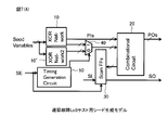
- FIG. 1 is a block diagram conceptually showing a conventional scan BIST LFSR seed generation method.
- a test pattern is generated by processing a netlist of a circuit under test (CUT) with an automatic test pattern generation tool (ATPG).
- the test pattern thus obtained is subjected to seed conversion to obtain a seed of LFSR.
- the seed of the LFSR is obtained through two-step processing (two-pass) of test pattern generation and seed generation.
- a test pattern may not be converted into a seed, and as a result, there is a problem that the fault detection rate is lowered.
- the present inventors considered that it is possible to create all seeds if ATPG can directly generate seeds without creating a test pattern from a netlist. .
- FIG. 2 is a block diagram conceptually showing the procedure of the one-pass seed creation method proposed by the present inventors.
- this method in order to create a seed directly by ATPG, a circuit obtained by artificially converting a circuit to be manufactured (CUT to be tested, CUT) from a netlist into a circuit suitable for producing a seed and converting the same Apply ATPG to generate seeds.
- the converted circuit is shown as a seed generation model.
- the LFSR used as a test pattern generator in the BIST and the state information of each scan FF of the sequential circuit which is a test circuit are temporally expanded.
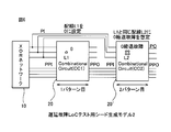
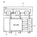
- FIG. 3 is a block diagram showing a subject BIST model.
- 1 indicates an LFSR
- 2 indicates a circuit under test (CUT)
- 3 indicates a response compressor (MISR).
- the CUT 2 is composed of a combinational circuit portion 20 of a sequential circuit and a scan FF chain 30.
- the response compressor 3 is not considered.
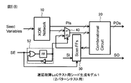
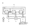
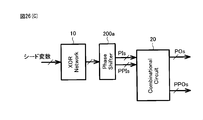
- FIG. 4 is a diagram showing the configuration of a seed generation model according to the first embodiment of the present invention.
- the model of this embodiment is a base model, and targets static faults.
- the combination circuit part of the sequential circuit is constructed by temporally expanding the BSR LFSR 1 by the longest scan path length of the scan FF 30 (see FIG. 3). Configured to connect to 20 inputs.
- the scan FF 30 is removed from the circuit under test (CUT) 2 shown in FIG. 3, the input from the original scan FF 30 to the combinational circuit portion 20 is a pseudo external input (PPIs).
- PPIs pseudo external input
- the outputs to the scan FF 30 of the above are assumed to be pseudo external outputs (PPOs).
- This model can simulate the same operation as the scan BIST circuit in the test mode. Therefore, if ATPG for a single stuck-at fault model or the like is applied to this seed generation model, as shown in FIG. 2, a seed for detecting a fault of the fault model without generating a test pattern for the CUT Can be determined directly.
- the XOR network will be described later with reference to FIGS. 8-10.
- FIGS. 5 (A), 5 (B), 6 and 7 (A) below show seed generation models for delay fault detection.
- the seed generation model shown in FIG. 5A is a seed generation model 1 for delay fault LoC test
- FIG. 6 shows a seed generation model 2 for delay fault LoC test
- the model shown in FIG. 7A is a seed generation model for the delay fault LoS test.
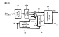
- the model shown in FIG. 5A is a seed generation model for testing delay faults in a launch-off capture (or broadside, hereinafter LoC) method, and shows a model corresponding to multi-clock capture.
- This model has a configuration in which a multiplexer 40 and a timing generation circuit 50 for temporally switching the input of the multiplexer 40 are added to the base model (XOR network 10 and combinational circuit portion 20) shown in FIG.
- the multiplexer 40 serves to switch the input signal to the combinational circuit portion 20 between the output of the XOR network 10 and the output of the scan FF 30.
- the multiplexer 40 is set to 1 during scan shift and during application of the first pattern, and to 0 during application of the second pattern (0 during capture in multi-cycle capture).
- FIG. 5B is a diagram showing another example of the model shown in FIG. 5A, which is a model for detecting delay faults in a two-pattern test (two-cycle capture).
- the circuit indicated by the dotted line 52 is an example of the timing generation circuit in the case of the two pattern test.
- FIG. 5C is a timing chart of test pattern loading in the LoC test corresponding to the two pattern test.
- the scan enable signal (SE) to 1 (scan shift mode) and apply the scan clock for a cycle of scan path length (the number of scan FFs in the longest scan path when there are multiple scan paths)
- SE scan enable signal
- SO scan output
- FIG. 6 shows a seed generation model 2 for LoC test.
- This model comprises an XOR network 10, a combinational circuit portion 20 of the circuit to be detected, and a second combinational circuit portion 20 'duplicating the combinational circuit portion 20.
- test generation of stuck-at faults can generate two pattern tests for delay faults.
- This uses a two-time expansion model. Duplicate two combination circuit parts, connect PI to both outputs of XOR network together, connect PPO of the first circuit and PPI of the second circuit and test two patterns only in combination circuit Can be generated.
- the first combinational circuit is the same portion as the signal line assuming a failure of the target circuit. It may be set to 0, and in the second combinational circuit, test generation may be performed on the same site assuming a 0 stuck-at fault.
- FIG. 7A shows a seed generation model for testing delay faults by a launch off shift (or skewed load, hereinafter, LoS) method.
- the second XOR network 10 ′ has a configuration in which a multiplexer 40 and a timing generation circuit 50 are added to temporally select the output of either XOR network 10 ′ and apply it to the combination circuit portion 20.
- the model shown corresponds to multi-clock capture, but if a circuit that outputs 1 when applying the first pattern and outputs 0 in synchronization with the second pattern capture clock is used as a timing generation circuit, it supports 2 pattern test Model.
- FIG. 7B shows a timing chart of test pattern loading in the LoS test corresponding to the two pattern test.
- the LoS test first, in scan shift mode, apply the scan clock for the scan path length cycle to shift in the first pattern of the 2 pattern test from the scan input and simultaneously shift out the response to the 2 pattern test. Do. Next, the scan clock is applied for one more cycle in the scan shift mode.
- the value set for the scan FF is the second pattern of the two pattern test.
- SE is set to 0 (normal operation mode) and a normal clock is applied for one cycle.
- the value loaded to the FF becomes a response to the two pattern test.
- the period from the last scan clock application to the normal clock application should be equal to the normal clock. Perform the test by repeating this.
- FIG. 8 is a diagram showing a sample circuit of 3-stage LFSR, 2 external inputs, and 3 scan path lengths.
- 81 indicates a 3-stage LFSR
- 82 indicates a CUT
- 83 indicates a combination circuit portion of the CUT 82
- 84 indicates a scan path of the CUT 82.
- the LFSR is configured by XOR and FF. Therefore, when the state information of the scan path 84 is temporally expanded, the circuit to be inspected can be considered as a combination circuit without an FF. Therefore, the values of each scan FF at a certain time and the external input can be expressed as a function of the seed.
- FIG. 10 shows an XOR network 101 formed based on the input / output relationship of FIG.
- FIG. 11 is a diagram showing a seed generation model configured by connecting the XOR network 101 shown in FIG. 10 to the combinational circuit portion 83 of the CUT, and the base model shown in FIG. 4 is applied to the sample circuit of FIG. It is a thing.
- the same operation as the scan BIST circuit in the test mode can be simulated, and ATPG is applied to this model. Can directly determine the seed. As a result, it is not necessary to generate a test with don't care, and the number of patterns can be reduced compared to the conventional method.
- FIG. 12 is a diagram showing a sample circuit of a 3-stage LFSR, 2 external inputs, and a scan path length of 3 and has 1 stuck-at fault in the combinational circuit portion.
- FIG. 13 shows an example of generating a seed for a target failure by the seed generation model formed for the circuit of FIG.
- FIG. 14 shows an example of test generation and seed conversion according to the conventional method, and shows a case where a test pattern: (0, X, X, 1, 1) can not be converted into a seed.
- LFSR linear feedback shift register
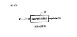
- FIG. 15A shows a combinational circuit
- FIG. 15B shows a sequential circuit
- a circuit that can be expressed as a combination of an input value, an output value, and an internal state value of 0 or 1 is called a logic circuit.
- Logic circuits can be further classified into combinational circuit (a) and sequential circuit (b).
- the output value of the circuit is determined only by the input value at that time, and in the sequential circuit, it is not determined only by the input value but depends on the internal state of the circuit.
- the combinational circuit consists only of the combinational component 152 as shown in FIG. 15 (A).
- PI and PO represent an external input and an external output, respectively.
- the sequential circuit as shown in FIG.
- the 15B comprises a state storage portion constituted by a combinational circuit portion 152 and a plurality of flip-flops (Flip-Flop, FF) 155.
- the output is determined by the value of the input currently applied and the value of the internal state.
- the internal state changes to the internal state at the next time according to the current input and the internal state.
- the D-type flip-flop 166 shown in FIG. 16 is handled.
- the FF 166 has a data input (D), a data output (Q) and a clock input (CLK), and takes in data by the clock signal.
- a failure model in which a logic function of a logic circuit changes to another logic function due to a failure is called a logic (static) failure.
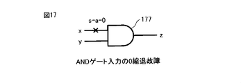
- a typical static fault model is stuck-at-fault.
- a stuck-at fault is a fault in which the value of the signal line in the circuit is fixed to 1 or 0, and a fault fixed to 1 is referred to as a stuck-at fault (stuck-at-1, sa-1), and is set to 0
- the fixed fault is called a stuck-at 0 fault (stuck-at-0, s-a-0).
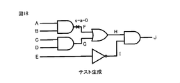
- a stuck-at fault consider the circuit shown in FIG.
- Testing is to make sure that the logic circuit is manufactured as designed.
- a test consists of two processes of test generation (test generation) and test execution (test application), assuming a failure in test generation, setting the value of the failure point opposite to the failure value (activation), Find a test pattern that propagates the value to the external output.
- test execution a test pattern obtained by test generation is applied to a circuit, and the presence or absence of a failure is determined by comparing the output response with an expected value.
- Test metrics include fault coverage and fault coverage.
- the failure detection rate is the number of failures that can be detected among the target failures, and is expressed by equation 1.
- the fault detection efficiency indicates how many faults have been detected among the targeted faults, as well as how many faults identified as faults that can not be detected by the I / O response called redundant faults are identified. It is a ratio and is expressed by equation 2.
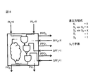
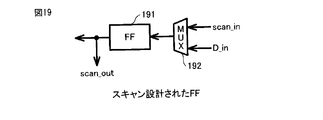
- FIG. 19 shows an example of the scan designed FF.
- One of the testability designs is scan design.
- FF 191 is provided with a scan input (scan in) so that it can be directly input from the outside, and multiplexer (MUX) 192 switches data input (Din) and scan input during normal operation so that they can be input to FF 191 .
- the output of the FF 191 can be observed from the scan out to the outside. If a scan input output terminal is prepared for each FF 191, an extra terminal is required twice as many as the number of FFs 191, which is not practical. Therefore, the FFs 191 are connected in a line so that they can operate as shift registers.
- a set of scan designed FFs in this way is called a scan path.
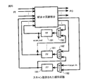
- FIG. 20 shows an example of a scan-designed sequential circuit.
- the FF 191 can be operated as a shift register, so that each FF 191 can be easily set to an arbitrary state, and at the same time, those states can be observed. Therefore, the problem of test generation of scan-designed circuits can be treated as a problem of combinational circuits.
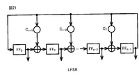
- FIG. 21 shows an example of the LFSR.
- a linear feed-back shift register (LFSR) is mainly used as a test pattern generation circuit of the built-in self-test system (BIST).
- BIST built-in self-test system
- the feedback position to XOR can be expressed by a polynomial, and the polynomial is called a characteristic polynomial.
- the characteristic polynomial of the LFSR in FIG. 21 can be expressed as Equation 3.
- the LFSR can be used to perform a pseudorandom test or an exhaustive test in which a pattern other than all zeros is applied.
- the value of the FF at the next time t + 1 can be expressed by the following equation 4 using the value of the FF at a certain time t and the characteristic polynomial.
- FIG. 22 shows a 3-bit LFSR.
- a design method that simplifies external test equipment is the built-in self-test (BIST) method.
- the BIST method uses a circuit that generates a test pattern and a circuit that examines an output response to the test pattern, and the pattern generation circuit mainly uses an LFSR.
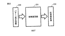
- FIG. 23 shows a schematic view of BIST.
- a test pattern is generated by the pattern generation circuit 230, applied to the circuit under test 231, and the output is compared with an expected value by the response analyzer (MISR) 231 to determine the presence or absence of a failure or a failure state.
- MISR response analyzer
- the pattern generation circuit 230 for example, the above-mentioned LFSR is used.
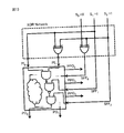
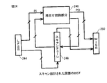
- FIG. 24 shows the BIST of the scan designed circuit.
- Reference numeral 244 denotes an LFSR as a pattern generator
- 246 denotes a combination circuit part in the sequential circuit
- 248 denotes a scan path formed of FFs in the sequential circuit
- 250 denotes an MISR as a response analyzer.
- a pseudorandom test is performed by moving the LFSR 244 until the scan path 248 is satisfied, and the values of the scan path 248 and PI at that time are applied to the combinational circuit portion 246 of the circuit under test .
- the BIST of this structure is used as the BIST model of the present application, as shown in FIG.
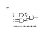
- One problem with BIST is that it is difficult to detect random pattern tolerant faults.
- a circuit in which the signal line E in FIG. 25 is sa-0 is shown.
- the pattern for detecting a fault needs a pattern in which all four inputs are 1; however, in the case of a 4-bit LFSR, the probability that this pattern is generated is 1/15.
- a failure that can be generated by the LFSR a failure that can be detected with only a limited number of patterns is called a random pattern tolerant failure.
- reseeding of LFSR referred to as reseed
- reseed is effective for detecting random pattern tolerant failure in BIST.
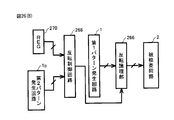
- phase shifter is a circuit created using an XOR arranged at the output of the LFSR, and it changes the order of patterns generated by the LFSR. Further, there is a method using a random inversion circuit as a technique for reducing the dependency between the FF, the external input, and the scan path as in the phase shifter.
- reference numeral 200 denotes a phase shifter, which serves to change the order of patterns generated by the LFSR 1 as described above.
- the BIST includes a circuit under test (CUT) 2, a scan path for enabling the scan, and a first pattern generation circuit 1 for forming a test pattern supplied to the scan path.
- the random inversion circuit controls pattern generation for changing the pattern generated by the first pattern generation circuit 1 using a pattern generated by the second pattern generation circuit 1 b provided separately from the first pattern generation circuit 1.
- the pattern control circuit includes an inversion logic unit 266 capable of inverting the logic of the output value of the first pattern generation circuit 1, and the inversion logic unit using a pattern generated by the second pattern generation circuit 1b.
- An inversion control circuit 268 capable of controlling the operation of the circuit 266 is included, and the output signal of the inversion logic unit 266 is supplied to the circuit under test 2. Specifically, whether the value generated by the first pattern generation circuit 1b is inverted is determined by the number of 1 values generated by the second pattern generation circuit 1b and the value of the inversion condition setting REG 270.
- the random inversion circuit is formed of the second pattern generation circuit 1b, the inversion logic unit 266, the inversion control circuit 268, and the inversion condition setting REG 270.
- FIG. 26 (C) and 26 (D) show a seed generation model corresponding to the BIST model with phase shifter shown in FIG. 26 (A).
- FIG. 26C shows a seed generation model with a phase shifter for static failure, in which a phase shifter group 200a is inserted between the XOR network 10 and the combinational circuit portion 20 with respect to the base model shown in FIG. Have.
- the phase shifter group 200a is a circuit in which the phase shifter 200 shown in FIG. 26A is copied in the scan path length and arranged in parallel. Strictly speaking, the phase shifter group 200a in FIGS. 26C and 26D has the phase shifter 200 shown in FIG.
- FIG. 26A shows a seed generation model with phase shifter for delay fault LoC test, in which the phase shifter group 200a is connected to the output of the XOR network 10 with respect to the seed generation model shown in FIG. 5A. It has composition.
- FIGS. 26E and 26F show a seed generation model corresponding to the BIST model with a random inversion circuit shown in FIG. 26B.
- FIG. 26E shows a seed generation model with a random inversion circuit for static failure, which is different from the base model shown in FIG. 4 in the second XOR network 10a, the inversion logic circuit group 266a, and the inversion control circuit group 268a. Equipped with The inversion logic circuit group 266a is a circuit in which the inversion logic unit 266 shown in FIG. 26B is copied in parallel for the scan path length and similarly arranged in the inversion control circuit group 268a. This is a circuit in which long copies are arranged in parallel.
- the second XOR network 10a is configured by expanding the time of the LFSR constituting the second pattern generation circuit 1b by the scan path length of the scan FF.
- the first seed input to the (first) XOR network 10 is the seed of the first pattern generation circuit 1 of FIG. 26B, and the second seed input to the second XOR network 10a. Is a seed to be input to the second pattern generation circuit 1b of FIG.
- FIG. 26F shows a seed generation model with a random inversion circuit for delay fault LoC test, and the second XOR network 10a and the inversion control circuit group 268a with respect to the seed generation model shown in FIG. 5A. , And a configuration in which a random inversion circuit group consisting of inversion logic circuit groups 266a is added.
- the seed input to the (first) XOR network 10 is the seed of the first pattern generation circuit 1
- the seed of the second XOR network 10a is the second pattern. It becomes a seed of the generation circuit 1b.
- a delay fault is a fault model in which a signal can not be propagated within a specified time due to the delay of a gate or a signal line and a malfunction occurs.
- Delay faults include transition faults, gate delay faults, and path delay faults. The following description is directed to transition faults, but is not limited thereto.
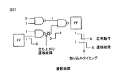
- FIG. 27 shows an example of transition failure. It is assumed that a transition fault causes a delay fault to occur in a certain signal line in a circuit, and that a delay large enough to be observed by an external output or an FF occurs regardless of a path propagating the delay. There are two types of transition faults: rising transition faults that delay the rise of the signal and falling transition faults that delay the fall.
- the transition fault test first, the value of the signal at the target point is set, then the value is changed, and the value is propagated to the external output or the FF, and the response is observed. For example, apply a pattern to set the signal line in the first pattern to 0 (low), apply a pattern to set the signal line to 1 (high) to the second pattern, and propagate it to the external output or FF By observing the change in value, it is possible to detect the rising transition fault of the signal line. Such a test method is called a two-pattern test.
- the LoC method and the LoS method as representative methods for performing two-pattern test at an actual speed (at-speed) in a scan-designed circuit.
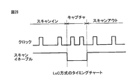
- the LoC test after the first pattern is set by the scan operation, the second pattern is set and the response is stored in the FF at the actual speed by the system clock (FIG. 28). This action is called capture.
- the first pattern is set in consideration of using the internal state for the signal set as the second pattern FF.
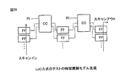
- a time expansion model in which the operation of the LoC method test is expanded for each time is shown in FIG.
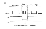
- the timing chart of the LoC method shown in FIG. 28 corresponds to the timing chart for explaining the operation of the delay fault LoC test seed generation model 1 shown in FIG. 5 (C).
- FIG. 30 shows a basic timing chart of the delay fault test according to the LoS method.
- This timing chart is basically the same as the timing chart (FIG. 7B) for explaining the operation of the seed generation model for delay fault LoS test according to the embodiment of the present invention shown in FIG. 7A. Therefore, it is possible to use the operation details of the LoS test as described in the description of FIGS. 7A and 7B.
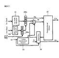
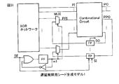
- FIG. 31 shows a seed generation model 1 for delay failure.
- the delay of the control signal m1 of the multiplexer of the seed generation circuit in the LoC test is shown in FIG.
- the delay fault seed generation model 1 of FIG. 31 is another embodiment of the delay fault seed generation model of FIG. 5 (A).
- a multiplexer is added to the output of the scan FF.
- the control signal of the multiplexer is the output of the FF added to the scan enable.
- the inputs of the multiplexer are the external input connecting the XOR network and the output from the scan FF.
- FIG. 6 shows the delay fault seed generation model 2
- FIG. 7 (A) shows the delay fault seed generation model 3 for the LoS test.
- the LFSR seed generation method of the present invention using the seed generation model (base model) for static failure and the seed generation models 1 to 3 for delay failure described above, seed generation is impossible in the seed generation model It is guaranteed that the failure (which turned out to be non-seed) could not be detected even by the original BIST circuit. Therefore, the fault detection capability of the BIST mechanism can be known.
- the test generation tool can be used to directly generate the seed by setting constraints on the test generation. In the conventional method, test generation and seed conversion operations are repeated until seed conversion can be performed. Therefore, in order to obtain the same failure detection rate as the proposed method, test generation is frequently retried and it takes time.
- #PIs, #POs, #Gates, and #FFs respectively represent the number of external inputs, the number of external outputs, the number of gates, and the number of FFs.
- the experimental method is shown below. First, 10,000 pseudo-random patterns are generated by LFSR using appropriate seeds, and failure simulation is performed on the circuit under test using the generated patterns. Next, as a result of failure simulation, the failure not detected is regarded as random pattern tolerant failure (RPRF), and the seed is obtained for each failure by the conventional method and the proposed method, and the failure detection rate and failure detection efficiency of both methods , Seed generation time, Seed number compared. In addition, the case where a phase shifter was attached to the LFSR was also evaluated. For test generation in this experiment, the abort time was set to 10 seconds. The abort time is the upper limit of the time taken to generate one pattern.
- RPRF random pattern tolerant failure
- the used LFSRs were 100 stages LFSR for the first pattern generation circuit without and with the random inversion circuit, and 10 stages for the second pattern generation circuit of the random inversion circuit.
- the phase shifter with the phase shifter is designed so that the input of each scan path is out of phase by more than the scan path length so that the same partial series generated from the LFSR does not enter the plurality of scan paths.
- the conversion to seed in the conventional method adopted the method of solving SAT, and used MiniSAT as a SAT solver.
- Table 4 shows the results of failure simulation with 10,000 pseudo random patterns using LFSR.
- Table 6 shows the results of failure simulation with 10,000 pseudo random patterns using the LFSR with a phase shifter.
- Table 7 shows the results of seed generation using the conventional method and the proposed method for the undetected faults in Table 6.
- Table 8 shows the results of failure simulation with 10,000 pseudo random patterns using LFSR with a random inversion circuit.
- Table 9 shows the results of seed generation using the conventional method and the proposed method for undetected faults in Table 8.
- the circuits used for the experiments are ITC'99 benchmark circuits b14, b17, b18, b19, b20, b21 and b22.
- the experimental environment is identical to that shown in Table 2.
- Tables 10 to 15 evaluation of seed single-piece quality by the seed generation model 1 for delay fault is described.
- Tables 10 and 11 show the evaluation environment and the circuit characteristics of the benchmark circuits b14, b17, b18, b19, b20, b21 and b22.
- Table 11 shows seed generation target faults. It shows the number of undetected failures after the initial pseudo random pattern application.
- Table 12 shows the results of experiments on seed single quality. Here, an undetected fault after application of 10,000 pseudo random patterns is a seed generation target.
- Table 13 shows test generation with don't care and seed conversion, and undetected faults after application of 10,000 pseudo random patterns are targets for seed generation. This shows the loss of fault coverage due to the inability to convert to seeds by the conventional method.
- Table 14 shows the cumulative failure detection rate / detection efficiency. This result shows the case including 10,000 pseudo random pattern application. Undetected faults after application of 10,000 pseudo random patterns are targets for seed generation.
- Tables 15 to 20 and FIGS. 33 to 36 below show experimental results of the seed deployment quality of the seeds generated using the delay generation function 1 for seed generation for delay faults.
- Table 15 shows the experimental result of seed quality (128 pattern expansion).
- the seeds are rearranged so that the rise of the detection rate becomes the fastest, the target generation target failure (only representative failure), the total failure and the undetected failure after applying 10,000 (10 k) pseudo random patterns for b21 For the b19, 50,000 (50 k) pseudo random pattern is not detected after application of the pseudo random pattern.
- Table 16 shows the status of seed generation.
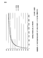
- FIG. 33 shows the transition of the detection rate for the total failure of b21.
- the experimental result shown in FIG. 34 shows the transition of the detection rate with respect to the undetected failure after applying the 10 k pseudo random pattern of b21.
- Table 18 show the transition of the detection rate for undetected faults after application of the 10 k pseudo random pattern of b21.
- the maximum detection rate reached by the conventional method is 85%, and the proposed method can reduce the number of seeds required to reach the same detection rate by 44% (44% reduction in test time).
- the experimental result shown in FIG. 35 is a figure which shows transition of the detection rate with respect to the undetected failure after 50k pseudo random pattern application of b19.
- Table 19 shows the transition of the detection rate for the undetected failure after applying the 50 k pseudo random pattern of b19.
- the maximum detection rate reached by the conventional method was 65%, and the proposed method was able to reduce the number of seeds required to reach this detection rate by 25% (25% reduction in test time).
- the experimental result shown in FIG. 36 shows the transition of the detection rate with respect to the undetected failure after applying the 50 k pseudo random pattern of b19.
Landscapes
- Engineering & Computer Science (AREA)
- General Engineering & Computer Science (AREA)
- Physics & Mathematics (AREA)
- General Physics & Mathematics (AREA)
- Tests Of Electronic Circuits (AREA)
- Semiconductor Integrated Circuits (AREA)
Applications Claiming Priority (6)
| Application Number | Priority Date | Filing Date | Title |
|---|---|---|---|
| JP2013148812 | 2013-07-17 | ||
| JP2013-148812 | 2013-07-17 | ||
| JP2013-148663 | 2013-07-17 | ||
| JP2013148663 | 2013-07-17 | ||
| JP2014-146027 | 2014-07-16 | ||
| JP2014146027A JP6391336B2 (ja) | 2013-07-17 | 2014-07-16 | スキャンbistのlfsrシード生成法及びそのプログラムを記憶する記憶媒体 |
Publications (1)
| Publication Number | Publication Date |
|---|---|
| WO2015008843A1 true WO2015008843A1 (ja) | 2015-01-22 |
Family
ID=52346285
Family Applications (1)
| Application Number | Title | Priority Date | Filing Date |
|---|---|---|---|
| PCT/JP2014/069103 Ceased WO2015008843A1 (ja) | 2013-07-17 | 2014-07-17 | スキャンbistのlfsrシード生成法及びそのプログラムを記憶する記憶媒体 |
Country Status (2)
| Country | Link |
|---|---|
| JP (1) | JP6391336B2 (enExample) |
| WO (1) | WO2015008843A1 (enExample) |
Families Citing this family (2)
| Publication number | Priority date | Publication date | Assignee | Title |
|---|---|---|---|---|
| JP7083728B2 (ja) * | 2018-08-24 | 2022-06-13 | ルネサスエレクトロニクス株式会社 | 自己診断装置、半導体装置及び自己診断方法 |
| JP2022017646A (ja) | 2020-07-14 | 2022-01-26 | ソニーセミコンダクタソリューションズ株式会社 | 固体撮像素子、車両制御システム、および、固体撮像素子の制御方法 |
Citations (2)
| Publication number | Priority date | Publication date | Assignee | Title |
|---|---|---|---|---|
| JPS55123744A (en) * | 1979-03-15 | 1980-09-24 | Nec Corp | Logic integrated circuit easy to check |
| US6611933B1 (en) * | 2000-04-12 | 2003-08-26 | International Business Machines Corporation | Real-time decoder for scan test patterns |
-
2014
- 2014-07-16 JP JP2014146027A patent/JP6391336B2/ja active Active
- 2014-07-17 WO PCT/JP2014/069103 patent/WO2015008843A1/ja not_active Ceased
Patent Citations (2)
| Publication number | Priority date | Publication date | Assignee | Title |
|---|---|---|---|---|
| JPS55123744A (en) * | 1979-03-15 | 1980-09-24 | Nec Corp | Logic integrated circuit easy to check |
| US6611933B1 (en) * | 2000-04-12 | 2003-08-26 | International Business Machines Corporation | Real-time decoder for scan test patterns |
Non-Patent Citations (2)
| Title |
|---|
| SATOSHI OTAKE ET AL.: "Sen'i Kosho BIST no Tameno Jikan Tenkai Model o Mochiita LFSR Seed Seiseiho", 4 DAIGAKU LSI TEST SEMINAR, 11 March 2013 (2013-03-11) * |
| T AKANORI MORIYASU ET AL.: "A Method of Deterministic LFSR Seed Generation for Scan- Based BIST", IEICE TECHNICAL REPORT, vol. 113, no. 104, 14 June 2013 (2013-06-14) * |
Also Published As
| Publication number | Publication date |
|---|---|
| JP2015038473A (ja) | 2015-02-26 |
| JP6391336B2 (ja) | 2018-09-19 |
Similar Documents
| Publication | Publication Date | Title |
|---|---|---|
| JP5537158B2 (ja) | 低消費電力スキャンテスト技術および装置 | |
| JP4177807B2 (ja) | 回路テストシステム | |
| US20120047412A1 (en) | Apparatus and system for implementing variable speed scan testing | |
| US11815555B2 (en) | Universal compactor architecture for testing circuits | |
| JP5034576B2 (ja) | 半導体集積回路、テストデータ生成装置およびlsi試験装置 | |
| EP3756020B1 (en) | Deterministic stellar built-in self-test | |
| US11585853B2 (en) | Trajectory-optimized test pattern generation for built-in self-test | |
| US6728914B2 (en) | Random path delay testing methodology | |
| Lala | An introduction to logic circuit testing | |
| EP3756021A1 (en) | Flexible isometric decompressor architecture for test compression | |
| JP6391336B2 (ja) | スキャンbistのlfsrシード生成法及びそのプログラムを記憶する記憶媒体 | |
| Girard et al. | Comparison between random and pseudo-random generation for BIST of delay, stuck-at and bridging faults | |
| Son et al. | E-BIST: Enhanced test-per-clock BIST architecture | |
| Kumar et al. | Implementation of hybrid LBIST mechanism in digital circuits for test pattern generation and test time reduction | |
| US11320487B1 (en) | Programmable test compactor for improving defect determination | |
| Holst et al. | Analysis and mitigation or IR-Drop induced scan shift-errors | |
| Chakraborty et al. | Path delay fault simulation of sequential circuits | |
| Gopikrishna et al. | Test Coverage Analysis of DFT with EDT and without EDT Architecture | |
| Pomeranz et al. | On the use of fully specified initial states for testing of synchronous sequential circuits | |
| Sowmya et al. | Strategic DFT Implementation and Verification of Next–Gen Electronics Using ATPG Simulation | |
| Oshima et al. | On Flip-Flop Selection for Multi-cycle Scan Test with Partial Observation in Logic BIST | |
| Balcárek et al. | On properties of sat instances produced by sat-based atpgs | |
| Kundu et al. | Diagnosing multiple faulty chains with low pin convolution compressor using compressed production test set | |
| Kalbande | Design of Fault Injection Technique for Digital HDL Models | |
| CN120344867A (zh) | 多阶段逻辑内建自测试观测扫描技术 |
Legal Events
| Date | Code | Title | Description |
|---|---|---|---|
| 121 | Ep: the epo has been informed by wipo that ep was designated in this application |
Ref document number: 14826147 Country of ref document: EP Kind code of ref document: A1 |
|
| NENP | Non-entry into the national phase |
Ref country code: DE |
|
| 122 | Ep: pct application non-entry in european phase |
Ref document number: 14826147 Country of ref document: EP Kind code of ref document: A1 |