WO2015005083A1 - 窒化物半導体積層基板、窒化物半導体装置および窒化物半導体積層基板の製造方法 - Google Patents
窒化物半導体積層基板、窒化物半導体装置および窒化物半導体積層基板の製造方法 Download PDFInfo
- Publication number
- WO2015005083A1 WO2015005083A1 PCT/JP2014/066197 JP2014066197W WO2015005083A1 WO 2015005083 A1 WO2015005083 A1 WO 2015005083A1 JP 2014066197 W JP2014066197 W JP 2014066197W WO 2015005083 A1 WO2015005083 A1 WO 2015005083A1
- Authority
- WO
- WIPO (PCT)
- Prior art keywords
- nitride semiconductor
- substrate
- layer
- semiconductor multilayer
- multilayer substrate
- Prior art date
- Legal status (The legal status is an assumption and is not a legal conclusion. Google has not performed a legal analysis and makes no representation as to the accuracy of the status listed.)
- Ceased
Links
Images



Classifications
-
- H—ELECTRICITY
- H10—SEMICONDUCTOR DEVICES; ELECTRIC SOLID-STATE DEVICES NOT OTHERWISE PROVIDED FOR
- H10D—INORGANIC ELECTRIC SEMICONDUCTOR DEVICES
- H10D62/00—Semiconductor bodies, or regions thereof, of devices having potential barriers
- H10D62/40—Crystalline structures
- H10D62/405—Orientations of crystalline planes
-
- H—ELECTRICITY
- H10—SEMICONDUCTOR DEVICES; ELECTRIC SOLID-STATE DEVICES NOT OTHERWISE PROVIDED FOR
- H10D—INORGANIC ELECTRIC SEMICONDUCTOR DEVICES
- H10D30/00—Field-effect transistors [FET]
- H10D30/01—Manufacture or treatment
- H10D30/015—Manufacture or treatment of FETs having heterojunction interface channels or heterojunction gate electrodes, e.g. HEMT
-
- H—ELECTRICITY
- H10—SEMICONDUCTOR DEVICES; ELECTRIC SOLID-STATE DEVICES NOT OTHERWISE PROVIDED FOR
- H10D—INORGANIC ELECTRIC SEMICONDUCTOR DEVICES
- H10D30/00—Field-effect transistors [FET]
- H10D30/40—FETs having zero-dimensional [0D], one-dimensional [1D] or two-dimensional [2D] charge carrier gas channels
- H10D30/47—FETs having zero-dimensional [0D], one-dimensional [1D] or two-dimensional [2D] charge carrier gas channels having two-dimensional [2D] charge carrier gas channels, e.g. nanoribbon FETs or high electron mobility transistors [HEMT]
- H10D30/471—High electron mobility transistors [HEMT] or high hole mobility transistors [HHMT]
- H10D30/475—High electron mobility transistors [HEMT] or high hole mobility transistors [HHMT] having wider bandgap layer formed on top of lower bandgap active layer, e.g. undoped barrier HEMTs such as i-AlGaN/GaN HEMTs
-
- H—ELECTRICITY
- H10—SEMICONDUCTOR DEVICES; ELECTRIC SOLID-STATE DEVICES NOT OTHERWISE PROVIDED FOR
- H10P—GENERIC PROCESSES OR APPARATUS FOR THE MANUFACTURE OR TREATMENT OF DEVICES COVERED BY CLASS H10
- H10P14/00—Formation of materials, e.g. in the shape of layers or pillars
- H10P14/20—Formation of materials, e.g. in the shape of layers or pillars of semiconductor materials
- H10P14/29—Formation of materials, e.g. in the shape of layers or pillars of semiconductor materials characterised by the substrates
- H10P14/2901—Materials
- H10P14/2902—Materials being Group IVA materials
- H10P14/2905—Silicon, silicon germanium or germanium
-
- H—ELECTRICITY
- H10—SEMICONDUCTOR DEVICES; ELECTRIC SOLID-STATE DEVICES NOT OTHERWISE PROVIDED FOR
- H10P—GENERIC PROCESSES OR APPARATUS FOR THE MANUFACTURE OR TREATMENT OF DEVICES COVERED BY CLASS H10
- H10P14/00—Formation of materials, e.g. in the shape of layers or pillars
- H10P14/20—Formation of materials, e.g. in the shape of layers or pillars of semiconductor materials
- H10P14/29—Formation of materials, e.g. in the shape of layers or pillars of semiconductor materials characterised by the substrates
- H10P14/2926—Crystal orientations
-
- H—ELECTRICITY
- H10—SEMICONDUCTOR DEVICES; ELECTRIC SOLID-STATE DEVICES NOT OTHERWISE PROVIDED FOR
- H10P—GENERIC PROCESSES OR APPARATUS FOR THE MANUFACTURE OR TREATMENT OF DEVICES COVERED BY CLASS H10
- H10P14/00—Formation of materials, e.g. in the shape of layers or pillars
- H10P14/20—Formation of materials, e.g. in the shape of layers or pillars of semiconductor materials
- H10P14/32—Formation of materials, e.g. in the shape of layers or pillars of semiconductor materials characterised by intermediate layers between substrates and deposited layers
- H10P14/3202—Materials thereof
- H10P14/3214—Materials thereof being Group IIIA-VA semiconductors
- H10P14/3216—Nitrides
-
- H—ELECTRICITY
- H10—SEMICONDUCTOR DEVICES; ELECTRIC SOLID-STATE DEVICES NOT OTHERWISE PROVIDED FOR
- H10P—GENERIC PROCESSES OR APPARATUS FOR THE MANUFACTURE OR TREATMENT OF DEVICES COVERED BY CLASS H10
- H10P14/00—Formation of materials, e.g. in the shape of layers or pillars
- H10P14/20—Formation of materials, e.g. in the shape of layers or pillars of semiconductor materials
- H10P14/34—Deposited materials, e.g. layers
- H10P14/3402—Deposited materials, e.g. layers characterised by the chemical composition
- H10P14/3414—Deposited materials, e.g. layers characterised by the chemical composition being group IIIA-VIA materials
- H10P14/3416—Nitrides
-
- H—ELECTRICITY
- H10—SEMICONDUCTOR DEVICES; ELECTRIC SOLID-STATE DEVICES NOT OTHERWISE PROVIDED FOR
- H10D—INORGANIC ELECTRIC SEMICONDUCTOR DEVICES
- H10D62/00—Semiconductor bodies, or regions thereof, of devices having potential barriers
- H10D62/80—Semiconductor bodies, or regions thereof, of devices having potential barriers characterised by the materials
- H10D62/85—Semiconductor bodies, or regions thereof, of devices having potential barriers characterised by the materials being Group III-V materials, e.g. GaAs
- H10D62/8503—Nitride Group III-V materials, e.g. AlN or GaN
-
- H—ELECTRICITY
- H10—SEMICONDUCTOR DEVICES; ELECTRIC SOLID-STATE DEVICES NOT OTHERWISE PROVIDED FOR
- H10D—INORGANIC ELECTRIC SEMICONDUCTOR DEVICES
- H10D64/00—Electrodes of devices having potential barriers
- H10D64/20—Electrodes characterised by their shapes, relative sizes or dispositions
- H10D64/23—Electrodes carrying the current to be rectified, amplified, oscillated or switched, e.g. sources, drains, anodes or cathodes
- H10D64/251—Source or drain electrodes for field-effect devices
- H10D64/256—Source or drain electrodes for field-effect devices for lateral devices wherein the source or drain electrodes are recessed in semiconductor bodies
-
- H—ELECTRICITY
- H10—SEMICONDUCTOR DEVICES; ELECTRIC SOLID-STATE DEVICES NOT OTHERWISE PROVIDED FOR
- H10H—INORGANIC LIGHT-EMITTING SEMICONDUCTOR DEVICES HAVING POTENTIAL BARRIERS
- H10H20/00—Individual inorganic light-emitting semiconductor devices having potential barriers, e.g. light-emitting diodes [LED]
- H10H20/80—Constructional details
- H10H20/81—Bodies
- H10H20/817—Bodies characterised by the crystal structures or orientations, e.g. polycrystalline, amorphous or porous
Definitions
- the present invention relates to a nitride semiconductor multilayer substrate, a nitride semiconductor device, and a method for manufacturing a nitride semiconductor multilayer substrate.
- Nitride semiconductor is represented by the general formula In x Al y Ga 1-x -y N (0 ⁇ x ⁇ 1,0 ⁇ y ⁇ 1,0 ⁇ x + y ⁇ 1). Since this nitride semiconductor can change the band gap in the range of 1.95 eV to 6 eV depending on its composition, it has been researched and developed as a material for light emitting devices in a wide wavelength range from the ultraviolet region to the infrared region. Has been.
- a control device using a nitride semiconductor is used for a power element that operates at high frequency and high output.
- a control device suitable for amplification in a high frequency band for example, a high electron mobility transistor (HEMT) is used.
- HEMT high electron mobility transistor
- Patent Document 1 JP 2008-166349 A (Patent Document 1).
- an AlN layer as a barrier layer an AlGaN layer as a buffer layer in which the Al composition is changed in the layer thickness direction, and a GaN layer are sequentially epitaxially grown on a Si substrate.
- the conventional nitride semiconductor multilayer substrate uses a Si substrate, it is less expensive than the case of using a sapphire substrate or a SiC (silicon carbide) substrate, and the AlN layer and the GaN layer Since an AlGaN layer having an Al composition changed in the layer thickness direction is sandwiched between them, there is an advantage that warpage and generation of cracks are small.
- the conventional nitride semiconductor multilayer substrate has a problem that pits are easily generated on the surface of the AlN layer formed on the Si substrate and the surface of the AlGaN layer immediately above the AlN.
- an object of the present invention is to provide a nitride semiconductor multilayer substrate, a nitride semiconductor device, and a method for manufacturing the nitride semiconductor multilayer substrate capable of suppressing the occurrence of pits in the nitride semiconductor layer. .
- the nitride semiconductor multilayer substrate of the present invention is A Si substrate having a main surface that is inclined at an off angle of 0.11 degrees or more and 0.50 degrees or less in the (011) direction from the (111) plane; And at least one nitride semiconductor layer epitaxially grown on the Si substrate.
- the nitride semiconductor device of the present invention is The above-mentioned nitride semiconductor multilayer substrate; A nitride semiconductor layer stacked on the nitride semiconductor multilayer substrate; And an electrode provided on the nitride semiconductor layer.
- the method for manufacturing the nitride semiconductor multilayer substrate of the present invention includes: Preparing a Si substrate whose main surface is a plane inclined at an off angle of 0.11 degree or more and 0.50 degree or less in the (011) direction from the (111) plane; And a step of epitaxially growing at least one nitride semiconductor layer on the main surface of the Si substrate.
- pits in the nitride semiconductor layer can be suppressed, and the characteristics of the nitride semiconductor device can be greatly improved.
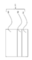
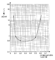
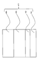
- FIG. 1 is a schematic cross-sectional view of a nitride semiconductor multilayer substrate according to a first embodiment of the present invention. It is a graph which shows the relationship between the off angle from the (111) plane of the main surface of a Si substrate to the (011) direction, and the number of pits. It is a cross-sectional schematic diagram of the nitride semiconductor multilayer substrate of 2nd Embodiment of this invention. It is a graph which shows the layer thickness and the number of pits of an Al layer. It is a cross-sectional schematic diagram of the nitride semiconductor multilayer substrate of 3rd Embodiment of this invention.
- HFET heterojunction field effect transistor
- a nitride semiconductor multilayer substrate 111 includes a Si substrate 101, an AlN layer 102 as an example of a nitride semiconductor layer epitaxially grown on the Si substrate 101, and the AlN layer 102.
- the AlGaN layer 103 is an example of a nitride semiconductor layer epitaxially grown thereon.
- the main surface of the Si substrate 101 is inclined from the (111) plane in the (011) direction with an off angle of 0.11 degrees or more and 0.50 degrees or less.
- the AlN layer 102 functions as a barrier layer, and the AlGaN layer 103 functions as a buffer layer.
- the nitride semiconductor e.g., GaN, said AlN, AlGaN, that of InGaN or the like, and more particularly, the general formula In x Al y Ga 1-x -y N (0 ⁇ x ⁇ 1, A semiconductor represented by 0 ⁇ y ⁇ 1, 0 ⁇ x + y ⁇ 1).
- Samples 1 and 5 below are comparative examples, and samples 2 to 4 are included in the first embodiment.
- a Si substrate (not shown) of Sample 1 whose main surface is a surface inclined at an off angle of 0.07 degrees in the (011) direction from the (111) plane; Si substrate 101 of sample 2 whose main surface is a plane inclined at an off angle of 0.11 degrees from the (111) plane to the (011) direction; Si substrate 101 of sample 3 whose main surface is a surface inclined at an off angle of 0.20 degrees in the (011) direction from the (111) plane; Si substrate 101 of sample 4 whose main surface is a surface inclined at an off angle of 0.50 degrees in the (011) direction from the (111) plane; Five types of sample Si substrates were prepared: a sample 5 Si substrate (not shown) whose main surface is a surface inclined at an off angle of 0.60 degrees from the (111) plane to the (011) direction.
- the Si substrates (not shown) of Samples 1 and 5 of the comparative example do not correspond to the Si substrate 101 shown in FIG. 1, while the Si substrates 101 of Samples 2 to 4 correspond to the Si substrate 101 shown in FIG. To do.
- the Si substrates of these five types of samples were treated with diluted hydrofluoric acid to remove the natural oxide film on the Si substrate. Thereafter, the Si substrate was introduced into a reactor of a MOCVD (Metal Organic Chemical Vapor Deposition) apparatus. Next, after raising the temperature of the Si substrate of the five types of samples to 1100 ° C., NH 3 (ammonia) and TMA (trimethylaluminum) are supplied, and an AlN layer 102 is grown on the main surface of the Si substrate at a growth rate of 400 nm. / Hr at 180 nm.
- MOCVD Metal Organic Chemical Vapor Deposition
- NH 3 , TMA, and TMG trimethylgallium are supplied while keeping the temperature of the Si substrate of the five types of samples at 1100 ° C., and an Al composition ratio of 0.6 nm is formed on the AlN layer 102.
- the AlGaN buffer layer 103 was epitaxially grown.
- a nitride semiconductor multilayer substrate in which the AlN layer 102 and the AlGaN buffer layer 103 are provided on the main surface of the Si substrate 101 was obtained.
- a nitride semiconductor multilayer substrate (sample 1-1: comparative example) using the Si substrate of sample 1 having an off angle of 0.07 degrees manufactured by the above-described manufacturing method;
- a nitride semiconductor multilayer substrate 111 (sample 1-2) using the Si substrate 101 of sample 2 having an off angle of 0.11 degrees as described above;
- a nitride semiconductor multilayer substrate 111 (sample 1-3) using the Si substrate 101 of sample 3 having the 0.20 degree off angle described above;
- For each of the five types of nitride semiconductor multilayer substrates with the above-described nitride semiconductor multilayer substrate 111 (sample 1-5: comparative example) using the Si substrate of the off angle of 0.60 degrees, an AlGaN layer The surface state of 103 was observed with an SEM (scanning electron microscope).
- Sample 1-1 is 15.5 pieces
- Sample 1-2 is 0.9 pieces
- Sample 1-3 is 0.5 pieces
- Sample 1-4 is 0.8 pieces
- Sample 1-5 was 11.3 pieces.
- nitride is obtained. It can be seen that the number of pits having a diameter of 10 nm or more and 50 nm or less can be remarkably reduced on the surface of the semiconductor laminated substrate 111. If the number of pits on the surface of the nitride semiconductor multilayer substrate 111 is small as in the first embodiment, the leakage current of a nitride semiconductor device (not shown) using the nitride semiconductor multilayer substrate 111 can be reduced.
- the off angle when the off angle is 0.11 degrees or more, the terrace width of the growth surface is shortened, the strain caused by the difference in lattice constant between AlN and Si can be easily relaxed, and threading dislocations are generated. Is presumed to be able to suppress pits resulting from threading dislocations.
- the off angle is larger than 0.50 degrees, AlN has a small ability to migrate the growth surface, so that nuclei are formed on the terrace and grow macroscopically in a three-dimensional manner. Dislocations are thought to occur in the meeting area.
- the Si substrate 101 has an off angle of 0.11 degrees or more and 0.50 degrees or less in the (011) direction from the (111) plane, the terrace width of the epitaxial growth surface is shortened. Further, it is possible to easily relax the strain caused by the difference in lattice constant between AlN and Si, to suppress the generation of threading dislocations, and to suppress the generation of pits resulting from threading dislocations.
- FIG. 3 is a schematic cross-sectional view of the nitride semiconductor multilayer substrate 211 of the second embodiment.
- the nitride semiconductor multilayer substrate 211 is formed by laminating an AlN layer 202 and an AlGaN layer 203 on an Si substrate 201. Become.
- the nitride semiconductor multilayer substrate 211 is produced by the same method as in the first embodiment, and an AlN layer 202 functioning as a barrier layer and an AlGaN layer 203 functioning as a buffer layer are sequentially epitaxially grown on the Si substrate 201. ing.
- the Si substrate 201 has a main surface inclined from the (111) plane in the (011) direction at an off angle of 0.20 degrees.
- the AlN layer 202 on the Si substrate 201 has a layer thickness of 40 nm (Sample 2-1). 50 nm (Sample 2-2), 100 nm (Sample 2-3), 180 nm (Sample 2-4), 400nm (Sample 2-5), 450 nm (Sample 2-6), Seven types of 500 nm (sample 2-7) were prepared, and the same AlGaN layer 203 was laminated on the AlN layer 202 to produce seven types of semiconductor laminated substrates 211.
- the surface state of the AlGaN layer 203 was observed with an SEM (scanning electron microscope) for each of the seven types of semiconductor multilayer substrates 211 described above.
- the average number in a 20 ⁇ m square area (5 locations) is: Sample 2-1, 25.6 Sample 2-2 is 1.3 pieces, Sample 2-3 is 0.8 pieces, Sample 2-4 has 0.5 pieces, Sample 2-5 is 1.4, Sample 2-6 is 13.8, Sample 2-7 was 21.7.
- the thickness of the AlN layer 202 is set to 50 nm or more and 400 nm or less.
- the Si substrate 201 has a main surface inclined at an off angle of 0.20 degrees in the (011) direction from the (111) plane, but the Si substrate 201 is separated from the (111) plane.
- the same tendency as in FIG. 4 was obtained even when the main surface was inclined at an off angle of 0.11 to 0.50 degrees in the (011) direction.
- a nitride semiconductor device (not shown) using the nitride semiconductor multilayer substrate 211 can reduce leakage current, etc. The electrical characteristics of can be improved.
- the AlN layer 202 when the thickness of the AlN layer 202 is thinner than 50 nm, the AlN layer 202 does not sufficiently function as a barrier layer, that is, a cover layer, and the TMG Ga used during the growth of the AlGaN layer 203 reacts with the Si substrate. Thus, it is presumed that the surface of the substrate is roughened, and threading dislocations that cause pits are more likely to occur.
- the thickness of the AlN layer 202 is larger than 400 nm, during the growth of the AlN layer 202 and the AlGaN layer 203, the warpage of the substrate due to the difference in lattice constant between Si and AlN increases, and the AlN layer 202, It is considered that strain was applied to the AlGaN layer 203 and pits were easily generated.
- FIG. 5 is a schematic cross-sectional view of the nitride semiconductor multilayer substrate 311 of the third embodiment.
- the nitride semiconductor multilayer substrate 311 is obtained by epitaxially growing an AlN layer 302 and an AlGaN layer 303 on a Si substrate 301.
- the nitride semiconductor multilayer substrate 311 is manufactured by the same method as in the first and second embodiments.
- an AlN layer 302 that functions as a barrier layer and an AlGaN layer 303 that functions as a buffer layer are formed. Sequentially epitaxial growth.
- the Si substrate 301 has a main surface inclined from the (111) plane in the (011) direction at an off angle of 0.20 degrees.
- the AlN layer 302 had a layer thickness of 180 nm, and samples with different half-value widths of rocking curves in (0002) plane X-ray diffraction were manufactured by changing the growth rate of the AlN layer 302.
- the half-value width of the rocking curve in the X-ray diffraction of the (0002) plane of the AlN layer 302 was adjusted by changing the growth rate when each AlN layer 302 was grown on the Si substrate 301.
- the half width of the rocking curve in the X-ray diffraction of the (0002) plane of the AlN layer 302 is 1900 arcsec (sample 3-1), 2200 arcsec (sample 3-2), 2500 arcsec (sample 3-3), Four types of nitride semiconductor multilayer substrates 311 with 2650 arcsec (sample 3-4) were manufactured.
- the surface state of the AlGaN layer 303 was observed with an SEM (scanning electron microscope) for each of the four types of nitride semiconductor multilayer substrates 311.
- the half width of the rocking curve in the X-ray diffraction of the (0002) plane of the AlN layer 302 on the Si substrate 301 is preferably 2500 arcsec or less.
- the Si substrate 301 has a main surface inclined at an off angle of 0.20 degrees in the (011) direction from the (111) plane, but the Si substrate 201 is separated from the (111) plane.
- the same tendency as in FIG. 6 can be obtained even if the main surface is an inclined surface with an off angle of 0.11 to 0.50 degrees in the (011) direction.
- the AlN layer 302 had a thickness of 180 nm. However, even when the thickness of the AlN layer 302 was not less than 50 nm and not more than 400 nm, substantially the same result as that obtained when the layer thickness was 180 nm was obtained.
- FIG. 7 is a schematic cross-sectional view of the nitride semiconductor multilayer substrate 411 of the fourth embodiment.
- the nitride semiconductor multilayer substrate 411 is obtained by epitaxially growing an AlN layer 102, an AlGaN layer 403, and a GaN layer 404 on a Si substrate 101 in order.
- the Si substrate 101 and the AlN layer 102 have the same configuration as the Si substrate 101 and the AlN layer 102 of the first embodiment, the same reference numerals as those in the first embodiment are used and detailed description thereof is omitted.
- the AlGaN layer 403 is an Al x Ga 1-x N layer (0.3 ⁇ x ⁇ 0.8). That is, the Al composition of the AlGaN layer 403 is 30% or more and 80% or less.
- the GaN layer 404 has a layer thickness of 100 nm or more.
- the nitride semiconductor multilayer substrate 411 having the above configuration warpage of the entire nitride semiconductor multilayer substrate 411 can be suppressed, and is given to the nitride semiconductor layer, that is, the AlN layer 102, the AlGaN layer 403, and the GaN layer 404. Distortion stress can be reduced and the occurrence of dislocations and pits can be suppressed.
- the nitride semiconductor multilayer substrate of the fifth embodiment has the same configuration as the nitride semiconductor multilayer substrate 111 of the first embodiment of FIG. 1 except for the surface of the Si substrate. Therefore, about the same component as the component of 1st Embodiment, FIG. 1 of 1st Embodiment is used.
- the Si substrate of the nitride semiconductor multilayer substrate of the fifth embodiment has a surface inclined from the (111) plane in the (011) direction at an off angle of 0.11 degrees or more and 0.50 degrees or less of the Si substrate.
- the surface of the Si substrate has irregularities so as to be 30% or more of the surface.
- the terrace width of the growth surface is shortened in a region of 30% or more of the surface of the Si substrate, and the strain caused by the difference in lattice constant between AlN and Si is alleviated. Therefore, the occurrence of threading dislocations can be reduced, and as a result, pits generated from threading dislocations can be suppressed. Therefore, if a nitride semiconductor device is made using this nitride semiconductor multilayer substrate, the leakage current can be reduced and the electrical characteristics can be improved.
- FIG. 8 is a cross-sectional view showing a main part of a heterojunction field effect transistor (HFET) of a sixth embodiment as an example of the nitride semiconductor device of the present invention.
- the Si substrate 101, the AlN layer 102, the AlGaN layer 103, and the nitride semiconductor multilayer substrate 111 are the Si substrate 101, the AlN layer 102, the AlGaN layer 103, and the nitride semiconductor multilayer substrate of the first embodiment shown in FIG. Since it has exactly the same configuration as 111, the same reference numerals as those in the first embodiment are assigned, and detailed description thereof is omitted.
- HFET heterojunction field effect transistor
- an undoped GaN layer 2 and an undoped AlGaN layer 3 are formed on the AlGaN layer 103 by epitaxial growth.
- the undoped GaN layer 2 and the undoped AlGaN layer 3 constitute a GaN-based laminate 5 having a heterojunction.
- 2DEG (two-dimensional electron gas) 6 is generated at the interface between the undoped GaN layer 2 and the undoped AlGaN layer 3.
- a recess reaching the undoped GaN layer 2 is formed in the GaN-based laminate 5, and the drain electrode 11 and the source electrode 12 are formed as ohmic electrodes in the recess.
- the drain electrode 11 and the source electrode 12 are Ti / Al / TiN electrodes in which a Ti layer, an Al layer, and a TiN layer are sequentially stacked.
- a gate electrode 13 is formed on the undoped AlGaN layer 3.
- the gate electrode 13 is, for example, a Schottky electrode that forms a Schottky junction with the undoped AlGaN layer 3 and is made of, for example, TiN.
- the gate electrode may be formed on an insulating film to have an insulated gate electrode structure.
- An interlayer insulating film (not shown) is formed on the undoped AlGaN layer 3, the drain electrode 11, the source electrode 12, and the gate electrode 13, and a drain electrode pad, a source electrode pad, and a gate electrode pad (not shown) are provided on the interlayer insulating film. ing.
- the drain electrode 11, the source electrode 12, and the gate electrode 13 are electrically connected to the drain electrode pad, the source electrode pad, and the gate electrode pad through via holes (not shown), respectively.
- the HFET of the sixth embodiment has the nitride semiconductor multilayer substrate 111 of the first embodiment, generation of pits due to threading dislocations can be suppressed, and therefore leakage current and the like can be reduced.
- the GaN-based stacked body 5 is configured by stacking the undoped GaN layer 2 and the undoped AlGaN layer 3, but the GaN-based stacked body is made of Al X In Y Ga 1-XY N. What is necessary is just to laminate
- the GaN-based laminate may include AlGaN, GaN, InGaN, or the like.
- a recess reaching the undoped GaN layer 2 is formed in the AlGaN layer 3, and the drain electrode 11 and the source electrode 12 are formed as ohmic electrodes in the recess.
- a drain electrode and a source electrode may be formed on the undoped AlGaN layer on the undoped GaN layer, and the drain electrode and the source electrode may be ohmic electrodes by reducing the thickness of the undoped AlGaN layer.
- the HFET has been described as an example of the nitride semiconductor device.
- the nitride semiconductor device of the present invention includes the nitride semiconductor multilayer substrates 111, 211, 311 of the first to fifth embodiments.
- HEMT High Electron Mobility Transistor: High Electron Mobility Transistor
- MISFET Metal-Insulator-Semiconductor Field Effect Transistor: Metal Insulator Semiconductor Field It may be an effect-transistor
- a junction FET an LED (light emitting diode), a semiconductor laser, or the like.
- the electrode may be a drain electrode, a source electrode, a gate electrode, an emitter electrode, a collector electrode, a base electrode, an anode electrode, a cathode electrode, or the like.
- the AlN layers 102, 202, and 302 are used as the barrier layer.
- a layer made of p-GaN, p-AlGaN, or the like can be used.
- the AlGaN layer as the buffer layer may change the Al composition in the layer thickness direction as in Patent Document 1.
- the nitride semiconductor multilayer substrates 111, 211, 311 and 411 of the present invention are: Si substrates 101, 201, 301 having a main surface as a main surface inclined at an off angle of 0.11 degrees or more and 0.50 degrees or less in the (011) direction from the (111) plane; It is characterized by comprising at least one nitride semiconductor layer 102, 103, 202, 203, 302, 303, 403, 404 epitaxially grown on the Si substrate 101, 201, 301.
- the Si substrates 101, 201, 301 have an off angle of 0.11 ° or more and 0.50 ° or less in the (011) direction from the (111) plane.
- the terrace width on the surface of the epitaxial growth is shortened, and for example, the distortion caused by the difference in lattice constant between AlN and Si can be easily relaxed, the occurrence of threading dislocations can be suppressed, and hence the pits generated from threading dislocations can be suppressed.
- the leakage current of the nitride semiconductor device using the nitride semiconductor multilayer substrates 111, 211, 311, 411, etc. can be reduced.
- An AlN layer 202 having a layer thickness of 50 nm or more and 400 nm or less is stacked on the Si substrate 201.
- the layer thickness of the AlN layer 203 is 50 nm or more and 400 nm or less, the reaction between Si and Ga is suppressed, for example, on the surface of the AlGaN layer 203, the diameter is 10 nm or more and 50 nm or less. The number of size pits can be significantly reduced.
- the half-value width of the rocking curve in the (0002) plane X-ray diffraction is 2500 arcsec or less.
- the half-value width of the rocking curve in the X-ray diffraction of the (0002) plane of the AlN layer 302 is 2500 arcsec or less, it is possible to suppress the occurrence of threading dislocations and hence the generation of pits. .
- the nitride semiconductor multilayer substrate 411 includes: An Al x Ga 1-x N layer 403 (0.3 ⁇ x ⁇ 0.8) is laminated on the AlN layer 102, A GaN layer 404 having a thickness of 100 nm or more is stacked on the Al x Ga 1-x N layer 403.
- warpage of the entire nitride semiconductor multilayer substrate 411 can be suppressed, strain stress applied to the nitride semiconductor layer, that is, the AlN layer 102, the AlGaN layer 403, and the GaN layer 404 can be reduced, Generation of dislocations and pits can be suppressed.
- the surface of the Si substrate so that the surface inclined at an off angle of 0.11 degree or more and 0.50 degree or less from the (111) plane to the (011) direction is 30% or more of the surface of the Si substrate. Have irregularities.
- the terrace width of the growth surface is shortened in a region of 30% or more of the surface of the Si substrate, the strain caused by the difference in lattice constant between AlN and Si can be easily relaxed, and threading dislocation occurs. As a result, pits resulting from threading dislocations can be suppressed. Therefore, the leakage current can be reduced.
- the off angle is increased, the surface roughness is increased, which is not preferable in the process step. If the off angle becomes too small, a difference in surface state such as a step interval and a step direction resulting from a slight off angle deviation occurs in the surface of the substrate.
- the off angle is preferably 0.11 degree or more and 0.50 degree or less from the viewpoint of the pit, and further, from the above viewpoint, the off angle is 0.2 degree or more and 0.4 degree or less. preferable.
- the nitride semiconductor device of the present invention is The aforementioned nitride semiconductor multilayer substrate 111; Nitride semiconductor layers 2 and 3 stacked on the nitride semiconductor multilayer substrate 111; Electrodes 11, 12, and 13 provided on the nitride semiconductor layers 2 and 3 are provided.
- the generation of pits due to threading dislocations can be suppressed and the leakage current can be reduced.
- the manufacturing method of the nitride semiconductor multilayer substrate of the present invention is as follows: A step of preparing Si substrates 101, 201, 301 having a main surface as a main surface inclined at an off angle of 0.11 degrees or more and 0.50 degrees or less in the (011) direction from the (111) plane; And a step of epitaxially growing at least one nitride semiconductor layer 102, 202, 302, 103, 203, 303, 403, 404 on the main surface of the Si substrate 101, 201, 301.
- a nitride semiconductor multilayer substrate of the present invention it is possible to obtain a nitride semiconductor multilayer substrate in which pits due to threading dislocations can be reduced and electrical characteristics such as leakage current are improved.
Landscapes
- Junction Field-Effect Transistors (AREA)
Abstract
窒化物半導体積層基板(111)は、(111)面から(011)方向に、0.11度以上、0.50度以下のオフ角で傾斜した面を主面とするSi基板(101)と、このSi基板(101)の上にエピタキシャル成長した少なくとも1つの窒化物半導体層(102,103)とを含む。
Description
この発明は、窒化物半導体積層基板、窒化物半導体装置および窒化物半導体積層基板の製造方法に関する。
窒化物半導体は、一般式InxAlyGa1-x-yN(0≦x≦1、0≦y≦1、0≦x+y≦1)で表される。この窒化物半導体は、その組成によって、バンドギャップを1.95eV~6eVの範囲で変化させることができることから、紫外域から赤外域に及ぶ広波長範囲の発光デバイスの材料として研究開発され、実用化されている。
また、窒化物半導体を用いた制御デバイスは、高周波かつ高出力で動作するパワー素子などに用いられており、中でも、高周波帯域での増幅に適した制御デバイスとして、例えば高電子移動度トランジスタ(HEMT)などのFETが知られている。
従来、窒化物半導体積層基板としては、特開2008-166349号公報(特許文献1)に記載のものがある。この従来の窒化物半導体積層基板は、Si基板上に、バリア層としてAlN層と、Al組成を層厚方向に変化させたバッファ層としてのAlGaN層と、GaN層を順次エピタキシャル成長している。
このように、上記従来の窒化物半導体積層基板は、Si基板を用いているから、サファイア基板やSiC(炭化シリコン)基板を用いる場合に比べて、安価であり、また、AlN層とGaN層との間に、Al組成を層厚方向に変化させたAlGaN層を挟み込んでいるから、反り、クラックの発生が少ないという利点を有する。
しかしながら、上記従来の窒化物半導体積層基板には、Si基板上に形成されたAlN層の表面、および、そのAlN直上のAlGaN層の表面にピットが発生しやすいという問題がある。
このピットは、SiとAlNの格子定数差から生じる貫通転位が発生起源になっていると考えられ、そのピット上にGaN層などの窒化物半導体層を成長させて、窒化物半導体装置を製造した場合、リーク等の要因となるため、発光デバイスならびに制御デバイスともに、その特性に悪い影響を与える。
そこで、この発明の課題は、窒化物半導体層にピットが発生するのを抑制することが可能な窒化物半導体積層基板、窒化物半導体装置および窒化物半導体積層基板の製造方法を提供することにある。
上記課題を解決するため、この発明の窒化物半導体積層基板は、
(111)面から(011)方向に、0.11度以上、0.50度以下のオフ角で傾斜した面を主面とするSi基板と、
このSi基板の上にエピタキシャル成長した少なくとも1つの窒化物半導体層と
を備えることを特徴としている。
(111)面から(011)方向に、0.11度以上、0.50度以下のオフ角で傾斜した面を主面とするSi基板と、
このSi基板の上にエピタキシャル成長した少なくとも1つの窒化物半導体層と
を備えることを特徴としている。
また、この発明の窒化物半導体装置は、
上述の窒化物半導体積層基板と、
上記窒化物半導体積層基板上に積層された窒化物半導体層と、
上記窒化物半導体層上に設けた電極と
を備えることを特徴としている。
上述の窒化物半導体積層基板と、
上記窒化物半導体積層基板上に積層された窒化物半導体層と、
上記窒化物半導体層上に設けた電極と
を備えることを特徴としている。
また、この発明の窒化物半導体積層基板の製造方法は、
(111)面から(011)方向に、0.11度以上、0.50度以下のオフ角で傾斜した面を主面とするSi基板を準備する工程と、
上記Si基板の主面の上に、少なくとも1つの窒化物半導体層をエピタキシャル成長する工程と
を備えることを特徴としている。
(111)面から(011)方向に、0.11度以上、0.50度以下のオフ角で傾斜した面を主面とするSi基板を準備する工程と、
上記Si基板の主面の上に、少なくとも1つの窒化物半導体層をエピタキシャル成長する工程と
を備えることを特徴としている。
この発明によれば、窒化物半導体層のピットを抑制することができて、窒化物半導体装置の特性を大幅に改善することができる。
(第1実施形態)(AlN層/Si基板 オフ角依存性)
図1に示すように、第1実施形態の窒化物半導体積層基板111は、Si基板101と、このSi基板101上にエピタキシャル成長した窒化物半導体層の一例としてのAlN層102と、このAlN層102上にエピタキシャル成長した窒化物半導体層の一例としてのAlGaN層103とからなる。
図1に示すように、第1実施形態の窒化物半導体積層基板111は、Si基板101と、このSi基板101上にエピタキシャル成長した窒化物半導体層の一例としてのAlN層102と、このAlN層102上にエピタキシャル成長した窒化物半導体層の一例としてのAlGaN層103とからなる。
上記Si基板101は、(111)面から(011)方向に、0.11度以上、0.50度以下のオフ角で傾斜した面を主面としている。
上記AlN層102は、バリア層として機能し、AlGaN層103は、バッファ層として機能する。
この明細書で、窒化物半導体とは、例えば、GaN、AlN、AlGaN、InGaN等のことを言い、より詳しくは、一般式InxAlyGa1-x-yN(0≦x≦1、0≦y≦1、0≦x+y≦1)で表される半導体のことを言う。
次に、上記窒化物半導体積層基板111の製造工程を、比較例と対比しつつ、説明する。下記のサンプル1,5は、比較例であり、サンプル2~4は、この第1実施形態に含まれるものである。
まず、Si基板のサンプルとして、
(111)面から(011)方向に、0.07度のオフ角度で傾斜した面を主面とするサンプル1のSi基板(図示せず)と、
(111)面から(011)方向に、0.11度のオフ角度で傾斜した面を主面とするサンプル2のSi基板101と、
(111)面から(011)方向に、0.20度のオフ角度で傾斜した面を主面とするサンプル3のSi基板101と、
(111)面から(011)方向に、0.50度のオフ角度で傾斜した面を主面とするサンプル4のSi基板101と、
(111)面から(011)方向に、0.60度のオフ角度で傾斜した面を主面とするサンプル5のSi基板(図示せず)と
の5種類のサンプルのSi基板を準備した。
(111)面から(011)方向に、0.07度のオフ角度で傾斜した面を主面とするサンプル1のSi基板(図示せず)と、
(111)面から(011)方向に、0.11度のオフ角度で傾斜した面を主面とするサンプル2のSi基板101と、
(111)面から(011)方向に、0.20度のオフ角度で傾斜した面を主面とするサンプル3のSi基板101と、
(111)面から(011)方向に、0.50度のオフ角度で傾斜した面を主面とするサンプル4のSi基板101と、
(111)面から(011)方向に、0.60度のオフ角度で傾斜した面を主面とするサンプル5のSi基板(図示せず)と
の5種類のサンプルのSi基板を準備した。
比較例のサンプル1,5のSi基板(図示せず)は、図1に示すSi基板101に相当しなく、一方、サンプル2~4のSi基板101は、図1に示すSi基板101に相当する。
この5種類のサンプルのSi基板を希釈フッ酸で処理し、Si基板の自然酸化膜を除去した。その後、Si基板をMOCVD(有機金属気相成長:Metal Organic Chemical Vapor Deposition)装置のリアクタ内に導入した。次に、5種類のサンプルのSi基板の温度を1100℃に昇温した後、NH3(アンモニア)およびTMA(トリメチルアルミニウム)を供給し、Si基板の主面に、AlN層102を成長速度400nm/hrで、180nm成長した。
次に、5種類のサンプルのSi基板の温度を1100℃にしたまま、NH3、TMAおよびTMG(トリメチルガリウム)を供給し、上記AlN層102上に、厚さ200nmでAl組成比0.6のAlGaNバッファ層103をエピタキシャル成長した。
以上の製造工程により、Si基板101の主面上に、AlN層102、AlGaNバッファ層103が設けられた窒化物半導体積層基板が得られた。
上記製造方法により製造した
上述の0.07度のオフ角度のサンプル1のSi基板を用いた窒化物半導体積層基板(サンプル1-1:比較例)と、
上述の0.11度のオフ角度のサンプル2のSi基板101を用いた窒化物半導体積層基板111(サンプル1-2)と、
上述の0.20度オフ角度のサンプル3のSi基板101を用いた窒化物半導体積層基板111(サンプル1-3)と、
上述の0.50度のオフ角度のサンプル4のSi基板を用いた窒化物半導体積層基板111(サンプル1-4)と、
上述の0.60度のオフ角度のサンプル5のSi基板を用いた窒化物半導体積層基板111(サンプル1-5:比較例)と
の5種類の窒化物半導体積層基板夫々に対して、AlGaN層103の表面状態をSEM(走査型電子顕微鏡)で観察した。
上述の0.07度のオフ角度のサンプル1のSi基板を用いた窒化物半導体積層基板(サンプル1-1:比較例)と、
上述の0.11度のオフ角度のサンプル2のSi基板101を用いた窒化物半導体積層基板111(サンプル1-2)と、
上述の0.20度オフ角度のサンプル3のSi基板101を用いた窒化物半導体積層基板111(サンプル1-3)と、
上述の0.50度のオフ角度のサンプル4のSi基板を用いた窒化物半導体積層基板111(サンプル1-4)と、
上述の0.60度のオフ角度のサンプル5のSi基板を用いた窒化物半導体積層基板111(サンプル1-5:比較例)と
の5種類の窒化物半導体積層基板夫々に対して、AlGaN層103の表面状態をSEM(走査型電子顕微鏡)で観察した。
その結果、AlGaN層103の表面において、直径10nm以上、50nm以下のサイズのピットの数について、20μm□エリア(5箇所)内の平均数は、
サンプル1-1は15.5個、
サンプル1-2は0.9個、
サンプル1-3は0.5個、
サンプル1-4は0.8個、
サンプル1-5は11.3個
であった。
サンプル1-1は15.5個、
サンプル1-2は0.9個、
サンプル1-3は0.5個、
サンプル1-4は0.8個、
サンプル1-5は11.3個
であった。
この状態を、図2に片対数グラフで示している。
この図2から、この第1実施形態にように、Si基板101が、(111)面から(011)方向に、0.11度以上、0.50度以下のオフ角を有すると、窒化物半導体積層基板111の表面において、直径10nm以上、50nm以下のサイズのピットの数が著しく低減できることが分かる。この第1実施形態のように、窒化物半導体積層基板111の表面のピット数が少ないと、この窒化物半導体積層基板111を用いた窒化物半導体装置(図示せず)のリーク電流を低減できる。
上記の現象に関して、上記オフ角が0.11度以上の場合は、成長表面のテラス幅が短くなり、AlNとSiの格子定数差から生じる歪を緩和しやすくでき、貫通転位の発生、しいては貫通転位から生じるピットを抑制することができると推定される。また、上記オフ角が0.50度より大きい場合は、AlNが成長表面をマイグレーションする能力が小さいため、テラス上に核が形成されて、マクロ的には3次元状に成長し、核同士が会合したエリアで転位が発生すると考えられる。
この第1実施形態では、Si基板101が、(111)面から(011)方向に、0.11度以上、0.50度以下のオフ角を有するので、エピタキシャル成長表面のテラス幅が短くなって、AlNとSiの格子定数差から生じる歪を緩和しやすくでき、貫通転位の発生を抑制でき、ひいては、貫通転位から生じるピットの発生を抑制することができる。
(第2実施形態)(AlN層/Si基板 AlN層層厚依存性)
図3は、第2実施形態の窒化物半導体積層基板211の断面模式図であり、この窒化物半導体積層基板211は、Si基板201上に、AlN層202と、AlGaN層203とを積層してなる。
図3は、第2実施形態の窒化物半導体積層基板211の断面模式図であり、この窒化物半導体積層基板211は、Si基板201上に、AlN層202と、AlGaN層203とを積層してなる。
上記窒化物半導体積層基板211は、第1実施形態と同様の方法で作製し、Si基板201上に、バリア層として機能するAlN層202と、バッファ層として機能するAlGaN層203とを順次エピタキシャル成長している。
詳細は、以下の通りである。上記Si基板201は、(111)面から(011)方向に、0.20度のオフ角で傾斜した面を主面としている。
上記Si基板201上のAlN層202は、層厚が
40nm(サンプル2-1)と、
50nm(サンプル2-2)と、
100nm(サンプル2-3)と、
180nm(サンプル2-4)と、
400nm(サンプル2-5)と、
450nm(サンプル2-6)と、
500nm(サンプル2-7)と
の7種類のものを作成し、それらのAlN層202上に、同じAlGaN層203を積層して、7種類の半導体積層基板211を製造した。
40nm(サンプル2-1)と、
50nm(サンプル2-2)と、
100nm(サンプル2-3)と、
180nm(サンプル2-4)と、
400nm(サンプル2-5)と、
450nm(サンプル2-6)と、
500nm(サンプル2-7)と
の7種類のものを作成し、それらのAlN層202上に、同じAlGaN層203を積層して、7種類の半導体積層基板211を製造した。
上述の7種類の半導体積層基板211の夫々に対して、AlGaN層203の表面状態をSEM(走査型電子顕微鏡)で観察した。
その結果、上記AlGaN層203の表面において、直径10nm以上、50nm以下のサイズのピットの数について、20μm□エリア(5箇所)内の平均数は、
サンプル2-1は25.6個、
サンプル2-2は1.3個、
サンプル2-3は0.8個、
サンプル2-4は0.5個、
サンプル2-5は1.4個
サンプル2-6は13.8個、
サンプル2-7は21.7個
であった。
サンプル2-1は25.6個、
サンプル2-2は1.3個、
サンプル2-3は0.8個、
サンプル2-4は0.5個、
サンプル2-5は1.4個
サンプル2-6は13.8個、
サンプル2-7は21.7個
であった。
この状態を、図4に片対数グラフで示している。
この図4から、AlN層203の層厚が50nm以上、400nm以下であると、AlGaN層203の表面において、直径10nm以上、50nm以下のサイズのピットの数が著しく減少することが分かる。この第2実施形態では、AlN層202の層厚を、50nm以上、400nm以下にしている。
なお、ここでは、上記Si基板201は、(111)面から(011)方向に、0.20度のオフ角で傾斜した面を主面としているが、Si基板201が、(111)面から(011)方向に、0.11から0.50度のオフ角で傾斜した面を主面としていても、図4と同じ傾向が得られた。
この第2施形態のように、窒化物半導体積層基板21の表面のピット数が少ないと、この窒化物半導体積層基板211を用いた窒化物半導体装置(図示せず)は、リーク電流の低減等の電気的な特性が改善できる。
上記の現象に関して、AlN層202の層厚が50nmより薄い場合、AlN層202がバリア層つまりカバー層として充分に機能せず、AlGaN層203の成長時に使用するTMGのGaとSi基板が反応して、基板表面を荒らして、ピット等の発生要因となる貫通転位が発生しやすくなったと推定される。
また、AlN層202の層厚が400nmよりも厚い場合、AlN層202およびAlGaN層203の成長中に、SiとAlNの格子定数差が要因となる基板の反りが大きくなって、AlN層202、AlGaN層203に歪応力が加わって、ピットが発生しやすくなったと考えられる。
(第3実施形態)(AlN層/Si基板 結晶性依存性)
図5は、第3実施形態の窒化物半導体積層基板311の断面模式図であり、この窒化物半導体積層基板311は、Si基板301上に、AlN層302、AlGaN層303をエピタキシャル成長してなる。
図5は、第3実施形態の窒化物半導体積層基板311の断面模式図であり、この窒化物半導体積層基板311は、Si基板301上に、AlN層302、AlGaN層303をエピタキシャル成長してなる。
上記窒化物半導体積層基板311は、第1および第2実施形態と同様の方法で作製し、Si基板301上に、バリア層として機能するAlN層302と、バッファ層として機能するAlGaN層303とを順次エピタキシャル成長している。
詳細は、以下の通りである。上記Si基板301は、(111)面から(011)方向に、0.20度のオフ角で傾斜した面を主面としている。上記AlN層302は、層厚が180nmであり、そのAlN層302の成長速度を変化させて、(0002)面のX線回折におけるロッキングカーブの半値幅が異なるサンプルを製造した。AlN層302の(0002)面のX線回折におけるロッキングカーブの半値幅の調整は、Si基板301上に、各AlN層302を成長させるときの成長速度を変化させて行った。
そして、AlN層302の(0002)面のX線回折におけるロッキングカーブの半値幅が
1900arcsec(サンプル3-1)と、
2200arcsec(サンプル3-2)と、
2500arcsec(サンプル3-3)と、
2650arcsec(サンプル3-4)と
の4種類の窒化物半導体積層基板311を製造した。
1900arcsec(サンプル3-1)と、
2200arcsec(サンプル3-2)と、
2500arcsec(サンプル3-3)と、
2650arcsec(サンプル3-4)と
の4種類の窒化物半導体積層基板311を製造した。
この4種類の窒化物半導体積層基板311の夫々に対して、AlGaN層303の表面状態をSEM(走査型電子顕微鏡)で観察した。
その結果、上記AlGaN層303の表面において、直径10nm以上、50nm以下のサイズのピットの数について、20μm□エリア(5箇所)内の平均数は、
サンプル3-1は0.5個、
サンプル3-2は0.8個、
サンプル3-3は1.8個、
サンプル3-4は12.3個、
であった。
サンプル3-1は0.5個、
サンプル3-2は0.8個、
サンプル3-3は1.8個、
サンプル3-4は12.3個、
であった。
この状態を、図6に片対数グラフで示している。
この図6から、Si基板301上のAlN層302の(0002)面のX線回折におけるロッキングカーブの半値幅は、2500arcsec以下が好ましいことが分かる。
この現象に関して、AlN層302の(0002)面のX線回折におけるロッキングカーブの半値幅が2500arcsecよりも大きくなると、結晶性が悪い場合に、ピットの要因となる貫通転位等が入り易くなったと考えられる。
逆に、上記AlN層302の(0002)面のX線回折におけるロッキングカーブの半値幅が2500arcsec以下であると貫通転位が比較的少なくなって、AlGaN層30を積層する際に、SiとGaの反応を抑制し、また結晶性が良好なため貫通転位の発生、ひいてはピットの発生を抑制することが可能となったと考えられる。
なお、ここでは、上記Si基板301は、(111)面から(011)方向に、0.20度のオフ角で傾斜した面を主面としているが、Si基板201が、(111)面から(011)方向に、0.11から0.50度のオフ角で傾斜した面を主面としていても、図6と同じ傾向が得られる。また、上記AlN層302は、層厚が180nmであったが、AlN層302の層厚が50nm以上、400nm以下であっても、層厚が180nmの場合と略同様の結果が得られた。
(第4実施形態)(GaN層/AlGaN層/AlN層/Si基板 AlN層混晶比、GaN層の層厚)
図7は、第4実施形態の窒化物半導体積層基板411の断面模式図である。この窒化物半導体積層基板411は、Si基板101上に、AlN層102とAlGaN層403とGaN層404とを順次エピタキシャル成長してなる。
図7は、第4実施形態の窒化物半導体積層基板411の断面模式図である。この窒化物半導体積層基板411は、Si基板101上に、AlN層102とAlGaN層403とGaN層404とを順次エピタキシャル成長してなる。
上記Si基板101およびAlN層102は、第1実施形態のSi基板101およびAlN層102と同じ構成を有するので、第1実施形態と同じ参照番号を付して、詳しい説明は省略する。
上記AlGaN層403は、AlxGa1-xN層(0.3≦x≦0.8)である。つまり、上記AlGaN層403のAl組成は、30%以上、80%以下である。また、上記GaN層404は、100nm以上の層厚を有する。
上記構成の窒化物半導体積層基板411によれば、その窒化物半導体積層基板411全体の反りを抑えることができて、窒化物半導体層、つまり、AlN層102,AlGaN層403,GaN層404に与える歪応力を低減して、転位およびピットの発生を抑制することができる。
(第5実施形態)(AlN層/Si基板 Si基板を凹凸加工)
この第5実施形態の窒化物半導体積層基板は、図示しないが、図1の第1実施形態の窒化物半導体積層基板111とは、Si基板の表面を除いて同じ構成を有する。したがって、第1実施形態の構成要素と同じ構成要素については、第1実施形態の図1を援用する。
この第5実施形態の窒化物半導体積層基板は、図示しないが、図1の第1実施形態の窒化物半導体積層基板111とは、Si基板の表面を除いて同じ構成を有する。したがって、第1実施形態の構成要素と同じ構成要素については、第1実施形態の図1を援用する。
この第5実施形態の窒化物半導体積層基板のSi基板は、(111)面から(011)方向に、0.11度以上、0.50度以下のオフ角で傾斜した面が上記Si基板の表面の30%以上となるように、上記Si基板の表面に凹凸を有する。
こうした場合でも、第1実施形態で検証した結果と略同じ結果が得られた。また、この第5実施形態のSi基板に、第2および第3実施形態と同じ窒化物半導体層を積層しても、第2および第3実施形態と略同じ効果が得られた。
この第5実施形態の窒化物半導体積層基板によれば、上記Si基板の表面の30%以上の領域で、成長表面のテラス幅が短くなって、AlNとSiの格子定数差から生じる歪を緩和しやすくでき、貫通転位の発生を少なくでき、ひいては貫通転位から生じるピットを抑制することができる。したがって、この窒化物半導体積層基板を用いて、窒化物半導体装置を作れば、リーク電流の減少等ができて、電気的特性を改善できる。
(第6実施形態)(窒化物半導体装置)
図8は、この発明の窒化物半導体装置の一例としての第6実施形態のヘテロ接合電界効果トランジスタ(HFET)の要部を示す断面図である。図8において、Si基板101、AlN層102、AlGaN層103および窒化物半導体積層基板111は、図1に示す第1実施形態のSi基板101、AlN層102、AlGaN層103および窒化物半導体積層基板111と全く同じ構成を有するので、第1実施形態と同じ参照番号を付して、その詳しい説明は省略する。
図8は、この発明の窒化物半導体装置の一例としての第6実施形態のヘテロ接合電界効果トランジスタ(HFET)の要部を示す断面図である。図8において、Si基板101、AlN層102、AlGaN層103および窒化物半導体積層基板111は、図1に示す第1実施形態のSi基板101、AlN層102、AlGaN層103および窒化物半導体積層基板111と全く同じ構成を有するので、第1実施形態と同じ参照番号を付して、その詳しい説明は省略する。
図8に示すように、この第6実施形態のHFETは、上記AlGaN層103上に、アンドープGaN層2、アンドープAlGaN層3をエピタキシャル成長により形成している。このアンドープGaN層2とアンドープAlGaN層3とがヘテロ接合を有するGaN系積層体5を構成している。上記アンドープGaN層2とアンドープAlGaN層3との界面に2DEG(2次元電子ガス)6が発生する。
また、上記GaN系積層体5には、アンドープGaN層2に達するリセスを形成し、このリセスにドレイン電極11とソース電極12とをオーミック電極として形成している。このドレイン電極11とソース電極12は、例えば、一例として、Ti層、Al層、TiN層が順に積層されたTi/Al/TiN電極である。また、上記アンドープAlGaN層3上に、ゲート電極13を形成している。このゲート電極13は、例えば、アンドープAlGaN層3とショットキー接合するショットキー電極であり、例えば、TiNで作製している。尤も、ゲート電極は、絶縁膜上に形成して、絶縁ゲート電極構造としてもよい。
上記アンドープAlGaN層3、ドレイン電極11、ソース電極12およびゲート電極13上に、図示しない層間絶縁膜を形成し、この層間絶縁膜上に図示しないドレイン電極パッド、ソース電極パッドおよびゲート電極パッドを設けている。そして、上記ドレイン電極11、ソース電極12およびゲート電極13を、夫々、図示しないビアホールを介して、ドレイン電極パッド、ソース電極パッドおよびゲート電極パッドに電気接続している。
この第6実施形態のHFETは、第1実施形態の窒化物半導体積層基板111を有するので、貫通転位に起因するピットの発生を抑制することができ、したがって、リーク電流等を低減できる。
なお、第1実施形態の窒化物半導体積層基板111に代えて、第2~第5実施形態の窒化物半導体積層基板211,311,411を用いても、同様の効果が得られる。
この第6実施形態では、GaN系積層体5は、アンドープGaN層2とアンドープAlGaN層3を積層して構成していたが、GaN系積層体は、AlXInYGa1-X-YN(X≧0、Y≧0、0≦X+Y<1)で表されるGaN系半導体層を積層したものであればよい。例えば、GaN系積層体は、AlGaN、GaN、InGaN等を含むものであってもよい。
また、この第6実施形態では、AlGaN層3に、アンドープGaN層2に達するリセスを形成し、このリセスにドレイン電極11とソース電極12をオーミック電極として形成したが、上記リセスを形成しないで、上記アンドープGaN層上のアンドープAlGaN層上にドレイン電極とソース電極を形成し、アンドープAlGaN層の層厚を薄くすることによってドレイン電極とソース電極がオーミック電極になるようにしてもよい。
この第6実施形態では、窒化物半導体装置の一例として、HFETについて説明したが、この発明の窒化物半導体装置は、第1~第5実施形態等の窒化物半導体積層基板111,211,311,411等を用いるものであればどのようなものであってもよく、例えば、HEMT(高電子移動度トランジスタ:High Electron Mobility Transistor)、MISFET(金属-絶縁体-半導体 電界効果トランジスタ:Metal Insulator Semiconductor Field Effect Transistor)、接合型FET、LED(発光ダイオード)、半導体レーザ等であってもよい。
また、窒化物半導体装置の種類に応じて、電極は、ドレイン電極、ソース電極、ゲート電極、エミッタ電極、コレクタ電極、ベース電極、アノード電極、カソード電極等となることは勿論である。
また、上記第1~第6実施形態では、バリア層としてAlN層102,202,302を用いていたが、それに代えて、例えば、p-GaN、p-AlGaN等からなる層を用いることができる。また、バッファ層としてのAlGaN層は、特許文献1のように、Al組成を層厚方向に変化させてもよい。
この発明および実施形態を纏めると、次のようになる。
この発明の窒化物半導体積層基板111,211、311,411は、
(111)面から(011)方向に、0.11度以上、0.50度以下のオフ角で傾斜した面を主面とするSi基板101,201,301と、
このSi基板101,201,301の上にエピタキシャル成長した少なくとも1つの窒化物半導体層102,103,202,203,302,303,403,404と
を備えることを特徴としている。
(111)面から(011)方向に、0.11度以上、0.50度以下のオフ角で傾斜した面を主面とするSi基板101,201,301と、
このSi基板101,201,301の上にエピタキシャル成長した少なくとも1つの窒化物半導体層102,103,202,203,302,303,403,404と
を備えることを特徴としている。
上記構成の窒化物半導体積層基板によれば、Si基板101,201,301が、(111)面から(011)方向に、0.11度以上、0.50度以下のオフ角を有するので、エピタキシャル成長表面のテラス幅が短くなって、例えばAlNとSiの格子定数差から生じる歪を緩和しやすくでき、貫通転位の発生を抑制でき、ひいては、貫通転位から生じるピットを抑制することができる。
このように、上記窒化物半導体積層基板111,211、311,411の表面のピット数が少ないので、この窒化物半導体積層基板111,211、311,411を用いた窒化物半導体装置のリーク電流等を低減できる。
1実施形態では、
上記Si基板201上に、層厚が50nm以上、400nm以下のAlN層202を積層している。
上記Si基板201上に、層厚が50nm以上、400nm以下のAlN層202を積層している。
上記実施形態によれば、AlN層203の層厚が50nm以上、400nm以下であるので、SiとGaとの反応を抑制して、例えば、AlGaN層203の表面において、直径10nm以上、50nm以下のサイズのピットの数を著しく減少することができる。
1実施形態では、
上記AlN層302は、(0002)面のX線回折におけるロッキングカーブの半値幅が2500arcsec以下である。
上記AlN層302は、(0002)面のX線回折におけるロッキングカーブの半値幅が2500arcsec以下である。
上記実施形態によれば、上記AlN層302の(0002)面のX線回折におけるロッキングカーブの半値幅が2500arcsec以下であるので、貫通転位の発生、ひいてはピットの発生を抑制することが可能となる。
1実施形態の窒化物半導体積層基板411は、
上記AlN層102上に、AlxGa1-xN層403(0.3≦x≦0.8)を積層し、
このAlxGa1-xN層403の上に、100nm以上の厚さのGaN層404を積層している。
上記AlN層102上に、AlxGa1-xN層403(0.3≦x≦0.8)を積層し、
このAlxGa1-xN層403の上に、100nm以上の厚さのGaN層404を積層している。
上記実施形態によれば、窒化物半導体積層基板411全体の反りを抑えることができて、窒化物半導体層、つまり、AlN層102,AlGaN層403,GaN層404に与える歪応力を低減して、転位およびピットの発生を抑制することができる。
1実施形態では、
(111)面から(011)方向に、0.11度以上、0.50度以下のオフ角で傾斜した上記面が上記Si基板の表面の30%以上となるように、上記Si基板の表面が凹凸を有する。
(111)面から(011)方向に、0.11度以上、0.50度以下のオフ角で傾斜した上記面が上記Si基板の表面の30%以上となるように、上記Si基板の表面が凹凸を有する。
上記実施形態によれば、上記Si基板の表面の30%以上の領域で、成長表面のテラス幅が短くなって、AlNとSiの格子定数差から生じる歪を緩和しやすくでき、貫通転位の発生を少なくでき、ひいては貫通転位から生じるピットを抑制することができる。したがって、リーク電流の減少等ができる。また、オフ角が大きくなると、表面粗さが大きくなるため、プロセス工程において好ましくない。また、オフ角が小さくなり過ぎると、基板面内にわずかなオフ角のずれから生じるステップ間隔、ステップ方向等の表面状態の差異が基板の面内に生じる。このため、オフ角は、ピットの観点からは、0.11度以上、0.50度以下が好適であるが、さらには、上記の観点から、0.2度以上、0.4度以下が好ましい。
この発明の窒化物半導体装置は、
上述の窒化物半導体積層基板111と、
上記窒化物半導体積層基板111上に積層された窒化物半導体層2,3と、
上記窒化物半導体層2、3上に設けた電極11,12,13と
を備えることを特徴としている。
上述の窒化物半導体積層基板111と、
上記窒化物半導体積層基板111上に積層された窒化物半導体層2,3と、
上記窒化物半導体層2、3上に設けた電極11,12,13と
を備えることを特徴としている。
この発明の窒化物半導体装置によれば、貫通転位に起因するピットの発生を抑制して、リーク電流を少なくすることができる。
この発明の窒化物半導体積層基板の製造方法は、
(111)面から(011)方向に、0.11度以上、0.50度以下のオフ角で傾斜した面を主面とするSi基板101,201,301を準備する工程と、
上記Si基板101,201,301の主面の上に、少なくとも1つの窒化物半導体層102,202,302,103,203,303,403,404をエピタキシャル成長する工程と
を備えることを特徴としている。
(111)面から(011)方向に、0.11度以上、0.50度以下のオフ角で傾斜した面を主面とするSi基板101,201,301を準備する工程と、
上記Si基板101,201,301の主面の上に、少なくとも1つの窒化物半導体層102,202,302,103,203,303,403,404をエピタキシャル成長する工程と
を備えることを特徴としている。
この発明の窒化物半導体積層基板の製造方法によれば、貫通転位に起因するピットを低減できて、リーク電流等の少ない電気的特性が改善された窒化物半導体積層基板を得ることができる。
上記第1~第6実施形態および変形例で述べた構成要素は、適宜、組み合わせてもよく、また、適宜、選択、置換、あるいは、削除してもよいのは、勿論である。
2,404 GaN層
3,103,203,303,403 AlGaN層
101,201,301 Si基板
102,202,302 AlN層
11 ドレイン電極
12 ソース電極
13 ゲート電極
111,211、311,411 窒化物半導体積層基板
3,103,203,303,403 AlGaN層
101,201,301 Si基板
102,202,302 AlN層
11 ドレイン電極
12 ソース電極
13 ゲート電極
111,211、311,411 窒化物半導体積層基板
Claims (5)
- (111)面から(011)方向に、0.11度以上、0.50度以下のオフ角で傾斜した面を主面とするSi基板(101,201,301)と、
このSi基板(101,201,301)の上にエピタキシャル成長した少なくとも1つの窒化物半導体層(102,103,202,203,302,303,403,404)と
を備えることを特徴とする窒化物半導体積層基板。 - 請求項1に記載の窒化物半導体積層基板において、
上記Si基板(201)上に、層厚が50nm以上、400nm以下のAlN層(202)を積層したことを特徴とする窒化物半導体積層基板。 - 請求項2に記載の窒化物半導体積層基板において、
上記AlN層(302)は、(0002)面のX線回折におけるロッキングカーブの半値幅が2500arcsec以下であることを特徴とする窒化物半導体積層基板。 - 請求項1から3の何れか1つに記載の窒化物半導体積層基板(111)と、
上記窒化物半導体積層基板(111)上に積層された窒化物半導体層(2,3)と、
上記窒化物半導体層(2,3)上に設けた電極(11,12,13)と
を備えることを特徴とする窒化物半導体装置。 - (111)面から(011)方向に、0.11度以上、0.50度以下のオフ角で傾斜した面を主面とするSi基板(101,201,301)を準備する工程と、
上記Si基板(101,201,301)の主面の上に、少なくとも1つの窒化物半導体層(102,202,302,103,203,303,403,404)をエピタキシャル成長する工程と
を備えることを特徴とする窒化物半導体積層基板の製造方法。
Applications Claiming Priority (2)
| Application Number | Priority Date | Filing Date | Title |
|---|---|---|---|
| JP2013-146715 | 2013-07-12 | ||
| JP2013146715A JP2016167473A (ja) | 2013-07-12 | 2013-07-12 | 窒化物半導体積層基板、窒化物半導体装置および窒化物半導体積層基板の製造方法 |
Publications (1)
| Publication Number | Publication Date |
|---|---|
| WO2015005083A1 true WO2015005083A1 (ja) | 2015-01-15 |
Family
ID=52279769
Family Applications (1)
| Application Number | Title | Priority Date | Filing Date |
|---|---|---|---|
| PCT/JP2014/066197 Ceased WO2015005083A1 (ja) | 2013-07-12 | 2014-06-18 | 窒化物半導体積層基板、窒化物半導体装置および窒化物半導体積層基板の製造方法 |
Country Status (2)
| Country | Link |
|---|---|
| JP (1) | JP2016167473A (ja) |
| WO (1) | WO2015005083A1 (ja) |
Citations (1)
| Publication number | Priority date | Publication date | Assignee | Title |
|---|---|---|---|---|
| JP2012015304A (ja) * | 2010-06-30 | 2012-01-19 | Sumitomo Electric Ind Ltd | 半導体装置 |
-
2013
- 2013-07-12 JP JP2013146715A patent/JP2016167473A/ja active Pending
-
2014
- 2014-06-18 WO PCT/JP2014/066197 patent/WO2015005083A1/ja not_active Ceased
Patent Citations (1)
| Publication number | Priority date | Publication date | Assignee | Title |
|---|---|---|---|---|
| JP2012015304A (ja) * | 2010-06-30 | 2012-01-19 | Sumitomo Electric Ind Ltd | 半導体装置 |
Also Published As
| Publication number | Publication date |
|---|---|
| JP2016167473A (ja) | 2016-09-15 |
Similar Documents
| Publication | Publication Date | Title |
|---|---|---|
| JP5634681B2 (ja) | 半導体素子 | |
| CN107799583B (zh) | 在异质基底上的第III族氮化物缓冲层结构的p型掺杂 | |
| JP4530171B2 (ja) | 半導体装置 | |
| KR102874457B1 (ko) | 반도체 박막 구조체 및 이를 포함하는 전자 소자 | |
| KR101418187B1 (ko) | 화합물 반도체 장치 및 그 제조 방법 | |
| JP6035721B2 (ja) | 半導体装置の製造方法 | |
| CN103828030B (zh) | 半导体元件、hemt元件、以及半导体元件的制造方法 | |
| JP2005158889A (ja) | 半導体素子形成用板状基体及びこの製造方法及びこれを使用した半導体素子 | |
| CN103715246A (zh) | 半导体装置 | |
| WO2013125185A1 (ja) | エピタキシャル基板、半導体装置及び半導体装置の製造方法 | |
| WO2013168371A1 (ja) | エピタキシャル基板、半導体装置及び半導体装置の製造方法 | |
| US8405067B2 (en) | Nitride semiconductor element | |
| US10332975B2 (en) | Epitaxial substrate for semiconductor device and method for manufacturing same | |
| US20120168771A1 (en) | Semiconductor element, hemt element, and method of manufacturing semiconductor element | |
| JP6244769B2 (ja) | 半導体装置及び半導体装置の製造方法 | |
| JP6089122B2 (ja) | 窒化物半導体積層体およびその製造方法並びに窒化物半導体装置 | |
| JP6205497B2 (ja) | 窒化物半導体の製造方法 | |
| JP5776344B2 (ja) | 半導体装置 | |
| JP2013033877A (ja) | 半導体素子、hemt素子、および半導体素子の製造方法 | |
| CN117916890B (zh) | 半导体装置以及半导体装置的制造方法 | |
| WO2015005083A1 (ja) | 窒化物半導体積層基板、窒化物半導体装置および窒化物半導体積層基板の製造方法 | |
| CN108428741A (zh) | 氮化镓半导体器件及其制作方法 |
Legal Events
| Date | Code | Title | Description |
|---|---|---|---|
| 121 | Ep: the epo has been informed by wipo that ep was designated in this application |
Ref document number: 14822770 Country of ref document: EP Kind code of ref document: A1 |
|
| NENP | Non-entry into the national phase |
Ref country code: DE |
|
| NENP | Non-entry into the national phase |
Ref country code: JP |
|
| 122 | Ep: pct application non-entry in european phase |
Ref document number: 14822770 Country of ref document: EP Kind code of ref document: A1 |