WO2014199676A1 - 導光体及びそれを備えた面状発光装置 - Google Patents
導光体及びそれを備えた面状発光装置 Download PDFInfo
- Publication number
- WO2014199676A1 WO2014199676A1 PCT/JP2014/055303 JP2014055303W WO2014199676A1 WO 2014199676 A1 WO2014199676 A1 WO 2014199676A1 JP 2014055303 W JP2014055303 W JP 2014055303W WO 2014199676 A1 WO2014199676 A1 WO 2014199676A1
- Authority
- WO
- WIPO (PCT)
- Prior art keywords
- light
- light guide
- guide plate
- diffusion pattern
- diffusing agent
- Prior art date
- Legal status (The legal status is an assumption and is not a legal conclusion. Google has not performed a legal analysis and makes no representation as to the accuracy of the status listed.)
- Ceased
Links
Images




Classifications
-
- G—PHYSICS
- G02—OPTICS
- G02B—OPTICAL ELEMENTS, SYSTEMS OR APPARATUS
- G02B6/00—Light guides; Structural details of arrangements comprising light guides and other optical elements, e.g. couplings
- G02B6/0001—Light guides; Structural details of arrangements comprising light guides and other optical elements, e.g. couplings specially adapted for lighting devices or systems
- G02B6/0011—Light guides; Structural details of arrangements comprising light guides and other optical elements, e.g. couplings specially adapted for lighting devices or systems the light guides being planar or of plate-like form
- G02B6/0033—Means for improving the coupling-out of light from the light guide
- G02B6/0035—Means for improving the coupling-out of light from the light guide provided on the surface of the light guide or in the bulk of it
- G02B6/004—Scattering dots or dot-like elements, e.g. microbeads, scattering particles, nanoparticles
- G02B6/0043—Scattering dots or dot-like elements, e.g. microbeads, scattering particles, nanoparticles provided on the surface of the light guide
-
- G—PHYSICS
- G02—OPTICS
- G02B—OPTICAL ELEMENTS, SYSTEMS OR APPARATUS
- G02B6/00—Light guides; Structural details of arrangements comprising light guides and other optical elements, e.g. couplings
- G02B6/0001—Light guides; Structural details of arrangements comprising light guides and other optical elements, e.g. couplings specially adapted for lighting devices or systems
- G02B6/0011—Light guides; Structural details of arrangements comprising light guides and other optical elements, e.g. couplings specially adapted for lighting devices or systems the light guides being planar or of plate-like form
- G02B6/0033—Means for improving the coupling-out of light from the light guide
- G02B6/0035—Means for improving the coupling-out of light from the light guide provided on the surface of the light guide or in the bulk of it
- G02B6/004—Scattering dots or dot-like elements, e.g. microbeads, scattering particles, nanoparticles
- G02B6/0041—Scattering dots or dot-like elements, e.g. microbeads, scattering particles, nanoparticles provided in the bulk of the light guide
-
- G—PHYSICS
- G02—OPTICS
- G02B—OPTICAL ELEMENTS, SYSTEMS OR APPARATUS
- G02B6/00—Light guides; Structural details of arrangements comprising light guides and other optical elements, e.g. couplings
- G02B6/0001—Light guides; Structural details of arrangements comprising light guides and other optical elements, e.g. couplings specially adapted for lighting devices or systems
- G02B6/0011—Light guides; Structural details of arrangements comprising light guides and other optical elements, e.g. couplings specially adapted for lighting devices or systems the light guides being planar or of plate-like form
- G02B6/0033—Means for improving the coupling-out of light from the light guide
- G02B6/005—Means for improving the coupling-out of light from the light guide provided by one optical element, or plurality thereof, placed on the light output side of the light guide
- G02B6/0051—Diffusing sheet or layer
-
- G—PHYSICS
- G02—OPTICS
- G02F—OPTICAL DEVICES OR ARRANGEMENTS FOR THE CONTROL OF LIGHT BY MODIFICATION OF THE OPTICAL PROPERTIES OF THE MEDIA OF THE ELEMENTS INVOLVED THEREIN; NON-LINEAR OPTICS; FREQUENCY-CHANGING OF LIGHT; OPTICAL LOGIC ELEMENTS; OPTICAL ANALOGUE/DIGITAL CONVERTERS
- G02F1/00—Devices or arrangements for the control of the intensity, colour, phase, polarisation or direction of light arriving from an independent light source, e.g. switching, gating or modulating; Non-linear optics
- G02F1/01—Devices or arrangements for the control of the intensity, colour, phase, polarisation or direction of light arriving from an independent light source, e.g. switching, gating or modulating; Non-linear optics for the control of the intensity, phase, polarisation or colour
- G02F1/13—Devices or arrangements for the control of the intensity, colour, phase, polarisation or direction of light arriving from an independent light source, e.g. switching, gating or modulating; Non-linear optics for the control of the intensity, phase, polarisation or colour based on liquid crystals, e.g. single liquid crystal display cells
- G02F1/133—Constructional arrangements; Operation of liquid crystal cells; Circuit arrangements
- G02F1/1333—Constructional arrangements; Manufacturing methods
- G02F1/1335—Structural association of cells with optical devices, e.g. polarisers or reflectors
- G02F1/1336—Illuminating devices
- G02F1/133602—Direct backlight
- G02F1/133606—Direct backlight including a specially adapted diffusing, scattering or light controlling members
-
- G—PHYSICS
- G02—OPTICS
- G02B—OPTICAL ELEMENTS, SYSTEMS OR APPARATUS
- G02B6/00—Light guides; Structural details of arrangements comprising light guides and other optical elements, e.g. couplings
- G02B6/0001—Light guides; Structural details of arrangements comprising light guides and other optical elements, e.g. couplings specially adapted for lighting devices or systems
- G02B6/0011—Light guides; Structural details of arrangements comprising light guides and other optical elements, e.g. couplings specially adapted for lighting devices or systems the light guides being planar or of plate-like form
- G02B6/0033—Means for improving the coupling-out of light from the light guide
- G02B6/005—Means for improving the coupling-out of light from the light guide provided by one optical element, or plurality thereof, placed on the light output side of the light guide
-
- G—PHYSICS
- G02—OPTICS
- G02B—OPTICAL ELEMENTS, SYSTEMS OR APPARATUS
- G02B6/00—Light guides; Structural details of arrangements comprising light guides and other optical elements, e.g. couplings
- G02B6/0001—Light guides; Structural details of arrangements comprising light guides and other optical elements, e.g. couplings specially adapted for lighting devices or systems
- G02B6/0011—Light guides; Structural details of arrangements comprising light guides and other optical elements, e.g. couplings specially adapted for lighting devices or systems the light guides being planar or of plate-like form
- G02B6/0033—Means for improving the coupling-out of light from the light guide
- G02B6/005—Means for improving the coupling-out of light from the light guide provided by one optical element, or plurality thereof, placed on the light output side of the light guide
- G02B6/0055—Reflecting element, sheet or layer
-
- G—PHYSICS
- G02—OPTICS
- G02B—OPTICAL ELEMENTS, SYSTEMS OR APPARATUS
- G02B6/00—Light guides; Structural details of arrangements comprising light guides and other optical elements, e.g. couplings
- G02B6/0001—Light guides; Structural details of arrangements comprising light guides and other optical elements, e.g. couplings specially adapted for lighting devices or systems
- G02B6/0011—Light guides; Structural details of arrangements comprising light guides and other optical elements, e.g. couplings specially adapted for lighting devices or systems the light guides being planar or of plate-like form
- G02B6/0033—Means for improving the coupling-out of light from the light guide
- G02B6/0058—Means for improving the coupling-out of light from the light guide varying in density, size, shape or depth along the light guide
- G02B6/0061—Means for improving the coupling-out of light from the light guide varying in density, size, shape or depth along the light guide to provide homogeneous light output intensity
-
- G—PHYSICS
- G02—OPTICS
- G02B—OPTICAL ELEMENTS, SYSTEMS OR APPARATUS
- G02B6/00—Light guides; Structural details of arrangements comprising light guides and other optical elements, e.g. couplings
- G02B6/0001—Light guides; Structural details of arrangements comprising light guides and other optical elements, e.g. couplings specially adapted for lighting devices or systems
- G02B6/0011—Light guides; Structural details of arrangements comprising light guides and other optical elements, e.g. couplings specially adapted for lighting devices or systems the light guides being planar or of plate-like form
- G02B6/0066—Light guides; Structural details of arrangements comprising light guides and other optical elements, e.g. couplings specially adapted for lighting devices or systems the light guides being planar or of plate-like form characterised by the light source being coupled to the light guide
- G02B6/0073—Light emitting diode [LED]
Definitions
- the present invention relates to a light guide used for a planar light emitting device.
- planar light emitting devices used for backlights of liquid crystal display devices include a direct type provided with a light source directly under a light guide plate (light guide) and an edge type provided with a light source on the side of the light guide plate. is there.
- an edge type is often employed from the viewpoint of reducing the number of members, reducing the weight, and reducing the thickness.
- edge type planar light emitting device light from a light source is incident on the light guide plate, and the incident light repeats total reflection in the light guide plate, and is provided on the back surface of the light guide plate (reflective surface facing the light emitting surface).
- Surface light emission is obtained by reflecting with fluorescent ink or lens shape and emitting from the light exit surface.
- the light emitted from the light guide plate is refracted according to Fresnel's law, and most of the light is emitted at an angle parallel to the light output surface of the light guide plate, so that a lot of outgoing light perpendicular to the light output surface can be obtained. Absent.
- a method of arranging an optical sheet on the light emitting surface side of the light guide plate or adding a diffusing agent to the light guide plate is used.
- an optical sheet when used, the number of parts increases, and material costs and assembly costs increase.
- a diffusing agent when used, it is difficult to adjust the concentration of the diffusing agent inside the light guide plate, and it is difficult to obtain uniform surface emission.
- the diffusing agent is uniformly dispersed inside the light guide plate, becomes brightest in the vicinity of the light source, and becomes darker with distance from the light source, so uniform surface emission cannot be obtained.
- Patent Document 1 a light diffusing dot is formed on at least one surface of a light guide plate, and two or more kinds of light diffusing dots having different sizes are irregularly formed in a region where the concealment ratio by the light diffusing dot is 50% or less.
- Patent Document 2 discloses a light guide plate formed by overlapping light guide layers having different diffusing agent concentrations with gradation in thickness.
- An object of the present invention is to provide a light guide that can obtain a large amount of emitted light perpendicular to the light emitting surface and obtain uniform surface light emission with an inexpensive configuration. It is another object of the present invention to provide a planar light emitting device including the light guide.
- the light guide of the present invention is a light diffusing formed by a plurality of dots or lines containing a first diffusing agent on at least one of a light emitting surface and a back surface facing the light emitting surface. It has a pattern, The light diffusion pattern is controlled by the size of the dot or the width of the line, and the density of the dot or line.
- the light diffusion pattern containing the first diffusing agent can provide a large amount of outgoing light perpendicular to the light outgoing surface with an inexpensive configuration. Further, uniform surface emission can be obtained by controlling the light diffusion pattern by the size of the dots or the width of the lines and the density of the dots or lines. For example, a high level luminance distribution required for a liquid crystal display device can be obtained.
- the number of optical sheetless or optical sheets can be reduced. And, by reducing the number of parts, material costs and assembly costs can be reduced. Furthermore, various problems that occur when the optical sheet is used, for example, optical sheet unevenness and optical sheet bending can be suppressed.
- FIG. 2 is a sectional view taken along line AA in FIG. 1. It is a top view of the light-guide plate of 1st Embodiment of this invention. It is a figure explaining an example of the luminance distribution of the light-guide plate of 1st Embodiment of this invention. It is a figure explaining an example of the luminance distribution of the light-guide plate of 1st Embodiment of this invention. It is a figure explaining an example of the luminance distribution of the light-guide plate of 1st Embodiment of this invention. It is a figure explaining an example of the luminance distribution of the light-guide plate of 1st Embodiment of this invention. It is a fragmentary sectional view of the planar light-emitting device of 3rd Embodiment of this invention.
- a backlight of a liquid crystal display device will be described as an example of a planar light emitting device.
- the planar light emitting device of the present invention can also be used for display devices that employ other optical shutter devices such as MEMS (Micro Electro Mechanical Systems).
- MEMS Micro Electro Mechanical Systems
- Members common to the embodiments are denoted by the same reference numerals, and redundant description is omitted.
- the technical features described in each embodiment can be implemented in appropriate combination within the possible range.
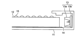
- FIG. 1 is a plan view of the planar light emitting device of this embodiment
- FIG. 2 is a cross-sectional view taken along line AA of FIG. 1
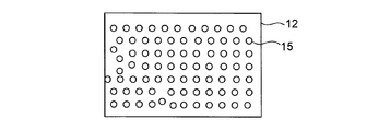
- FIG. 3 is a plan view of the light guide plate of this embodiment.
- the planar light emitting device 10 includes a backlight chassis 11, a light guide plate (light guide) 12, a light source unit 13, and a reflection sheet 14.
- Various optical sheets may be provided on the light guide plate 12 as appropriate.
- the optical sheet is a generic term for a prism sheet, a diffusion sheet, and the like, and is a combination of one or a plurality of these sheets.
- the backlight chassis 11 is a member that serves as a base for mounting (accommodating) each member of the planar light emitting device 10.
- SECC steel plate
- aluminum or the like for the material of the backlight chassis 11, it is desirable to use SECC (steel plate), aluminum or the like in order to ensure rigidity and heat dissipation.
- the light guide plate 12 is a member that converts light incident from the light incident surface into a surface light source and derives it from the light emitting surface.
- the light guide plate 12 is, for example, a rectangular parallelepiped, and has a light emitting surface facing a liquid crystal panel (not shown), a surface facing the light emitting surface (back surface), and four side surfaces connecting these two surfaces. Of the four side surfaces, two side surfaces (two surfaces on the long side in FIG. 1) are light incident surfaces that face each light source unit 13. Note that the light incident surface may be at least one side surface, and the light source units 13 may be provided in a number opposite to the light incident surface.
- a resin such as acrylic, polystyrene, PC (polycarbonate), or glass from the viewpoint of thickness reduction and weight reduction.
- the light source unit 13 is disposed to face the light incident surface of the light guide plate 12. Such an arrangement of the light source unit 13 is called an edge type and can be made thinner than the direct type.
- the light source unit 13 includes an LED (Light Emitting Diode) 13a, which is a point light source, and an LED substrate 13b on which the LED is mounted. A plurality of LEDs 13a are arranged along the side surface of the light guide plate 12 at predetermined intervals on the LED substrate 13b to form a linear light source.
- a metal substrate such as Al is preferably used in consideration of heat dissipation and strength.
- you may use the fluorescent tube etc. which are linear light sources other than LED.
- the reflection sheet 14 is disposed on the surface side (back surface side) facing the light emitting surface of the light guide plate 12. The light that reaches the back surface in the light guide plate 12 is reflected by the reflection sheet 14, and the light emission efficiency of the light guide plate 12 is improved.
- the light guide plate 12 has a light diffusion pattern formed by a plurality of dots 15 containing the first diffusing agent on the light exit surface. This light diffusion pattern is controlled (determined) by the size of the dots 15 and the density of the dots 15 so that uniform surface emission can be obtained.
- the light propagating in the light guide plate 12 changes its propagation angle by the dots 15, and light having an angle component smaller than the critical angle is extracted from the light exit surface.
- the dots 15 diffuse light by mainly reflecting the light in the light guide plate 12 to increase the light extraction efficiency.
- the dots 15 can have a circular shape or the like, and are formed, for example, by printing a white paint containing the first diffusing agent with an inkjet or the like.
- the shape of the dot 15 is not limited and may be an ellipse or a polygon. In the case of inkjet printing, it becomes a semi-spherical shape, but it can be made into an arbitrary shape by using screen printing or the like.
- the first diffusing agent is not limited in material and shape as long as it diffuses light, and for example, silica micro beads can be used. In addition, fine particles such as silicone, zirconia, titanium dioxide, and calcium carbonate can be used. Further, the degree of diffusion can be adjusted by adjusting the concentration of the first diffusing agent in the light diffusion pattern.
- the light diffusion pattern is determined by the size of the dots 15 and the density of the dots 15 as described above, but the brightness distribution can be adjusted more precisely as the distance between the dots 15 is shorter, that is, the density of the dots 15 is higher.
- the distance between the dots 15 is preferably 100 ⁇ m or less.
- the size of the dots 15 is too large, the luminance distribution cannot be adjusted precisely.
- the size is too small, it is difficult to obtain the effect of light diffusion.
- the light diffusion pattern may have a shape other than the dot 15, for example, a stripe-like or curved line (a line having a width).
- a stripe-like or curved line a line having a width
- the light diffusion pattern is controlled by the line width and the line density.
- the luminance distribution can be precisely adjusted by shortening the distance between the lines and setting the line width to an appropriate range.
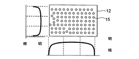
- FIG. 4 to 6 are diagrams for explaining an example of the luminance distribution of the light guide plate of the present embodiment.
- the light guide plate 12 shown in FIG. 4 has a light diffusion pattern formed by dots 15, and the luminance is the highest in the vicinity of the center in both the longitudinal direction and the lateral direction, and the luminance increases from the center toward both ends. Smoothly lowered. The difference between the luminance near the center and the luminance near both ends is within 20%. According to such a luminance distribution, the high level luminance distribution required for the liquid crystal display device is satisfied.
- the light guide plate 12 shown in FIG. 5 has a light diffusion pattern formed by dots 15, and the luminance in the vicinity of the center is the highest in both the longitudinal direction and the lateral direction, and the luminance increases from the center toward both ends. Slightly lower and the brightness rapidly decreases near both ends. The difference between the luminance near the center and the luminance near both ends is within 20%. Such a luminance distribution also satisfies a high-level luminance distribution required for a liquid crystal display device.
- the light guide plate 12 shown in FIG. 6 has a light diffusion pattern in which stripe-like lines 16 are formed vertically and horizontally, and has a luminance distribution similar to that in FIG. Such a light diffusion pattern can also provide a high-level luminance distribution required for a liquid crystal display device.
- the light diffusion pattern even if the light diffusion pattern is provided on the back surface of the light guide plate 12, the same effect can be obtained. Moreover, you may provide a light-diffusion pattern in both a light-projection surface and a back surface. That is, the light diffusion pattern may be formed on at least one of the light exit surface of the light guide plate 12 and the back surface facing the light exit surface.
- the light guide plate 12 of the present embodiment has a light diffusing pattern formed by the plurality of dots 15 or lines 16 containing the first diffusing agent on at least one of the light emitting surface and the back surface facing the light emitting surface.
- the light diffusion pattern is controlled by the size of the dot 15 or the width of the line 16 and the density of the dot 15 or the line 16.
- the light diffusion pattern containing the first diffusing agent can provide a large amount of outgoing light perpendicular to the light outgoing surface with an inexpensive configuration. Further, by controlling the light diffusion pattern by the size of the dots 15 or the width of the lines 16 and the density of the dots 15 or the lines 16, uniform surface light emission can be obtained. For example, a high level luminance distribution required for a liquid crystal display device can be obtained. By using such a light guide plate 12, the number of optical sheetless or optical sheets can be reduced. And, by reducing the number of parts, material costs and assembly costs can be reduced. Furthermore, various problems that occur when the optical sheet is used, for example, optical sheet unevenness and optical sheet bending can be suppressed.
- a second diffusing agent is contained in the light guide plate 12 other than the light diffusion pattern in the first embodiment.
- Other configurations are the same as those of the first embodiment.
- the second diffusing agent is not limited in material and shape as long as it diffuses light.
- silica micro beads can be used.
- the same fine particles as the first diffusing agent can be used.
- the degree of diffusion can be adjusted by adjusting the concentration of the second diffusing agent in the light guide plate 12.
- the second diffusing agent may be uniformly dispersed inside the light guide plate 12, and there is no need to adjust the concentration of the diffusing agent within the light guide plate 12. Therefore, the light guide plate 12 to which the second diffusing agent is added can be easily manufactured at low cost.
- the second diffusing agent by adding the second diffusing agent to the inside of the light guide plate 12, light propagating in the light guide plate 12 is diffused by the second diffusing agent. As a result, light perpendicular to the light exit surface increases, and more emitted light perpendicular to the light exit surface can be obtained. At this time, since the outgoing light from between the light diffusion patterns increases on the light outgoing surface, the luminance difference from the outgoing light from the light diffusion pattern is reduced, and the display quality is improved.
- the concentration of the first diffusing agent in the light diffusion pattern and the concentration of the second diffusing agent in the light guide plate 12 are adjusted so as to obtain uniform surface light emission.
- the concentration of the second diffusing agent is preferably such a concentration that the light from the LED 13a propagates to the entire light guide plate 12, while the concentration of the first diffusing agent increases the light extraction efficiency while increasing the light extraction efficiency.
- the concentration is preferably such that uniform surface emission can be obtained by the diffusion pattern.
- the concentration of the first diffusing agent in the light diffusing patterns is the light guide plate 12. It is preferable that the concentration is equal to or greater than the concentration of the second diffusing agent in the interior and that the concentration difference is small.
- the concentration of the first diffusing agent in the light diffusion pattern is preferably 1 to 1.1 times the concentration of the second diffusing agent in the light guide plate 12, and preferably 1 to 1.05 times. More preferably.
- FIG. 7 is a partial cross-sectional view of the planar light emitting device of this embodiment. As shown in FIG. 7, the third embodiment differs from the first embodiment in that a film 21 having a light diffusion pattern is used. Other configurations are the same as those of the first embodiment.
- the light guide plate 20 is configured by adhering a film 21 having a light diffusion pattern on the light emitting surface side with an adhesive or the like.
- the main body of the light guide plate 20 excluding the film 21 can use the same material as the light guide plate 12 of the first embodiment.
- a material of the film 21 a material that can be used for the light guide plate 20 can be used.
- the refractive index of the film 21 is substantially equal to the refractive index of the light-guide plate 20 main body from a viewpoint of improving light extraction efficiency. Therefore, it is preferable to use the same material for the film 21 and the light guide plate 20.
- the light diffusion pattern can be the same as in the first embodiment, and for example, dots 15 are used in FIG. Further, as in the second embodiment, a second diffusing agent may be added inside the light guide plate 20.
- the same effect can be obtained even if the film 21 is provided on the back surface of the light guide plate 20.
- the manufacturing speed is improved as compared with the case of printing directly on the light guide plate. And it becomes easy to process a light-diffusion pattern into the film 21 of a large area, and the response
- the light guide (light guide plate 12) of one embodiment of the present invention is formed by a plurality of dots 15 or lines 16 containing the first diffusing agent on at least one of the light exit surface and the back surface facing the light exit surface.
- the light diffusion pattern is controlled by the size of the dot 15 or the width of the line 16 and the density of the dot 15 or line 16.
- the light diffusing pattern containing the first diffusing agent can provide a large amount of outgoing light perpendicular to the light outgoing surface with an inexpensive configuration. Further, by controlling the light diffusion pattern by the size of the dots 15 or the width of the lines 16 and the density of the dots 15 or the lines 16, uniform surface light emission can be obtained. For example, a high level luminance distribution required for a liquid crystal display device can be obtained.
- a light guide light guide plate 12
- the number of optical sheets or optical sheets can be reduced. And, by reducing the number of parts, material costs and assembly costs can be reduced. Furthermore, various problems that occur when the optical sheet is used, for example, optical sheet unevenness and optical sheet bending can be suppressed.
- a second diffusing agent is contained inside the light guide other than the light diffusion pattern.
- the second diffusing agent may be uniformly dispersed inside the light guide, and there is no need to adjust the concentration of the diffusing agent within the light guide. Therefore, the light guide added with the second diffusing agent can be easily manufactured at low cost. Further, by adding the second diffusing agent inside the light guide, the light propagating through the light guide is diffused by the second diffusing agent. As a result, light perpendicular to the light exit surface increases, and more emitted light perpendicular to the light exit surface can be obtained. At this time, since the emitted light from between the light diffusion patterns increases on the light exit surface, the luminance difference from the light emitted from the light diffusion pattern is reduced, and the display quality is improved.
- the concentration of the first diffusing agent in the light diffusion pattern is preferably 1 to 1.1 times the concentration of the second diffusing agent in the light guide.
- the luminance difference between the light emitted from between the light diffusion patterns and the light emitted from the light diffusion pattern on the light emission surface is small and bright spots are not easily generated, so the luminance uniformity is high and the display quality is high. improves.
- the light guide may have a structure in which the film 21 having the light diffusion pattern is attached.
- the manufacturing speed is improved as compared with the case of printing directly on the light guide. To do. And it becomes easy to process a light-diffusion pattern into the film 21 of a large area, and the response
- the planar light-emitting device 10 includes a light guide body according to any one of the above, in which one side surface other than the light emitting surface and the back surface is a light incident surface, and is opposed to the light incident surface. And a light source (LED 13a).
- an edge-type planar light-emitting device that can be used as a backlight for a liquid crystal display device or the like can be provided.
- the present invention can be used in a display device that employs an optical shutter device such as a liquid crystal panel or MEMS.
Landscapes
- Physics & Mathematics (AREA)
- General Physics & Mathematics (AREA)
- Optics & Photonics (AREA)
- Nonlinear Science (AREA)
- Mathematical Physics (AREA)
- Chemical & Material Sciences (AREA)
- Crystallography & Structural Chemistry (AREA)
- Planar Illumination Modules (AREA)
Abstract
安価な構成で、光出射面に対して垂直な出射光が多く得られるとともに、均一な面発光を得ることができる導光体を提供することを目的とする。そのため、導光板は、光出射面及び該光出射面に対向する裏面の少なくとも一方に、第1拡散剤を含有した複数のドットで形成される光拡散パターンを有し、該光拡散パターンはドットの大きさと、ドットの密度とによって制御されることを特徴とする。
Description
本発明は、面状発光装置に用いる導光体に関する。
従来から、液晶表示装置のバックライトなどに用いられる面状発光装置には、光源を導光板(導光体)の直下に備える直下型と、光源を導光板の側方に備えるエッジ型とがある。一般的に、部材の削減、軽量化、薄型化等の観点からエッジ型が採用されることが多い。
エッジ型の面状発光装置では、光源からの光を導光板へ入射させ、入射した光が導光板内で全反射を繰り返し、導光板の裏面(光出射面に対向する反射面)に設けた蛍光インクやレンズ形状などで反射し、光出射面から出射することで面発光を得ている。しかしながら、導光板から出射する光はフレネルの法則によって屈折し、多くは導光板の光出射面に対して平行に近い角度で出射するため、光出射面に対して垂直な出射光は多く得られない。
この対策としては、導光板の光出射面側に光学シートを配設したり、導光板に拡散剤を添加したりする手法が用いられている。しかし、光学シートを用いた場合は部品点数が増え、材料費及び組立費が増加する。一方、拡散剤を用いた場合は導光板内部で拡散剤の濃度を調整することが難しく、均一な面発光を得ることが難しい。通常、拡散剤は導光板内部で均一に分散してしまい、光源付近で最も明るくなり、光源から離れるにしたがって暗くなるので、均一な面発光が得られない。
ところで、特許文献1には、導光板の少なくとも一方の面に光拡散ドットを形成し、光拡散ドットによる隠蔽率が50%以下の領域に2種類以上の大きさの異なる光拡散ドットを不規則に並べた構成が開示されている。また、特許文献2には、拡散剤の濃度が異なる導光層を厚みにグラデーションをもたせて重ねることで形成した導光板が開示されている。
しかしながら、特許文献1の技術では、導光板の光出射面に対して垂直な出射光は多く得られない。また、特許文献2の技術では、拡散剤の濃度が異なる導光層が複数必要なため、多くの材料が必要となり高価になる。さらに、各層を完全に密着させる必要があり、製造が困難である。
本発明は、安価な構成で、光出射面に対して垂直な出射光が多く得られるとともに、均一な面発光を得ることができる導光体を提供することを目的とする。また、その導光体を備えた面状発光装置を提供することも目的とする。
上記目的を達成するために本発明の導光体は、光出射面及び該光出射面に対向する裏面の少なくとも一方に、第1拡散剤を含有した複数のドット又はラインで形成される光拡散パターンを有し、該光拡散パターンは前記ドットの大きさ又は前記ラインの幅と、前記ドット又はラインの密度とによって制御されることを特徴とする。
本発明によると、第1拡散剤を含有した光拡散パターンにより、安価な構成で、光出射面に対して垂直な出射光が多く得られる。また、光拡散パターンをドットの大きさ又はラインの幅と、ドット又はラインの密度とによって制御することにより、均一な面発光を得ることができる。例えば、液晶表示装置に要求される高水準の輝度分布を得ることができる。このような導光体を用いることによって、光学シートレス又は光学シートの枚数を減らすことができる。そして、部品点数が削減されることで、材料費及び組立費を削減できる。さらに、光学シートを用いることで発生する種々の問題、例えば、光学シートムラや光学シート撓みを抑制できる。
以下に本発明の実施形態を図面を参照して説明する。以下の実施形態では面状発光装置として液晶表示装置のバックライトを例に説明する。なお、本発明の面状発光装置は、MEMS(Micro Electro Mechanical Systems)等、他の光シャッターデバイスを採用する表示装置などにも利用できる。各実施形態で共通する部材には同符号を付し、重複する説明を省略する。また、各実施形態で記載されている技術特徴は可能な範囲で適宜組み合わせて実施することができる。
<第1実施形態>
図1は、本実施形態の面状発光装置の平面図であり、図2は、図1のA-A線断面図であり、図3は、本実施形態の導光板の平面図である。
図1は、本実施形態の面状発光装置の平面図であり、図2は、図1のA-A線断面図であり、図3は、本実施形態の導光板の平面図である。
面状発光装置10は、バックライトシャーシ11と、導光板(導光体)12と、光源ユニット13と、反射シート14とを備えている。なお、導光板12上に適宜、各種光学シートを設けてもよい。光学シートは、プリズムシート、拡散シート等の総称であり、これらのシートの何れか1枚又は複数枚を組み合わせたものである。
バックライトシャーシ11は、面状発光装置10の各部材を搭載(収容)するための土台となる部材である。バックライトシャーシ11の材料には、剛性及び放熱性を確保するため、SECC(鋼板)やアルミニウムなどを用いることが望ましい。
導光板12は光入射面から入射した光を面光源へ変換して光出射面から導出する部材である。導光板12は例えば直方体であり、液晶パネル(不図示)に対向する光出射面と、該光出射面に対向する面(裏面)と、それら2面を繋ぐ4つの側面とを有する。4つの側面のうち2つの側面(図1では長辺側の2面)は各光源ユニット13に対向する光入射面である。なお、光入射面は少なくとも1つの側面であればよく、光源ユニット13も光入射面に対向する数だけ設置すればよい。導光板12の材料としては薄型化、軽量化の観点からアクリル、ポリスチレン、PC(ポリカーボネート)などの樹脂やガラスを用いることが望ましい。
光源ユニット13は、導光板12の光入射面に対向して配設される。このような光源ユニット13の配置はエッジ型と呼ばれ、直下型よりも薄型化できる。光源ユニット13は点状光源であるLED(Light Emitting Diode)13aと、LEDを搭載するLED基板13bとを含んでいる。そして、LED基板13b上で複数のLED13aが導光板12の側面に沿って所定間隔で配設されて線状光源を形成している。LED基板13bとしては放熱性や強度を考慮してAlなどの金属基板を用いることが好ましい。なお、光源としては、LEDの他に線状光源である蛍光管などを用いてもよい。
反射シート14は、導光板12の光出射面に対向する面側(裏面側)に配設される。反射シート14により、導光板12内で裏面に到達した光が反射され、導光板12の発光効率が向上する。
次に、本実施形態の特徴的な構成について説明する。導光板12は光出射面に、第1拡散剤を含有した複数のドット15で形成される光拡散パターンを有している。この光拡散パターンは、均一な面発光が得られるように、ドット15の大きさと、ドット15の密度とによって制御(決定)されている。導光板12内の光はドット15によって伝搬する角度が変化し、臨界角よりも小さい角度成分をもった光が光出射面から取り出される。
ドット15は、導光板12内の光を主に反射させることで拡散させて光の取り出し効率を高めるものである。ドット15は円形等の形状とすることができ、例えば、第1拡散剤を含んだ白色の塗料をインクジェット等で印刷することで形成される。なお、ドット15の形状には限定はなく、楕円形や多角形であってもよい。インクジェット印刷の場合は半円球状となるが、スクリーン印刷等を用いれば任意の形状にすることができる。
第1拡散剤は、光を拡散すれば材料や形状等に限定はなく、例えば、シリカの微小ビーズを用いることができる。他にはシリコーン、ジルコニア、二酸化チタン、炭酸カルシウムなどの微粒子を用いることもできる。また、光拡散パターンにおける第1拡散剤の濃度を調整することで拡散度合いを調整できる。
光拡散パターンは、上述したようにドット15の大きさと、ドット15の密度とによって決められるが、ドット15間の距離が短いほど、つまりドット15の密度が高いほど輝度分布を精密に調整できる。例えば、ドット15間の距離は100μm以下であることが好ましい。また、ドット15の大きさは、大きすぎると輝度分布を精密に調整できず、逆に小さすぎると光拡散の効果が得られにくいため、50~80μmであることが好ましい。
さらに、光拡散パターンはドット15以外の形状であってもよく、例えば、ストライプ状や湾曲状等のライン(幅をもった線)などであってもよい。このようなラインを用いる場合、光拡散パターンはラインの幅と、ラインの密度とによって制御される。そして、ドット15を用いる場合と同様に、ライン間の距離を短く、ラインの幅を適切な範囲にすることで輝度分布を精密に調整できる。
図4~図6は、本実施形態の導光板の輝度分布の一例を説明する図である。図4に示した導光板12は、ドット15で形成される光拡散パターンを有しており、長手方向及び短手方向ともに、中央付近の輝度が最も高く、中央から両端へ向かってそれぞれ輝度が滑らかに低くなっている。そして、中央付近の輝度と両端付近の輝度の差が20%以内となっている。このような輝度分布によれば、液晶表示装置に要求される高水準の輝度分布を満たしている。
図5に示した導光板12は、ドット15で形成される光拡散パターンを有しており、長手方向及び短手方向ともに、中央付近の輝度が最も高く、中央から両端へ向かってそれぞれ輝度がやや低くなり、両端付近で急激に輝度が低くなっている。そして、中央付近の輝度と両端付近の輝度の差が20%以内となっている。このような輝度分布によっても、液晶表示装置に要求される高水準の輝度分布を満たしている。
図6に示した導光板12は、ストライプ状のライン16が縦横に直交して形成される光拡散パターンを有しており、図5と同様の輝度分布となっている。このような光拡散パターンによっても液晶表示装置に要求される高水準の輝度分布が得られる。
なお、本実施形態において光拡散パターンは導光板12の裏面に設けても同じ効果が得られる。また、光拡散パターンは光出射面及び裏面の両方に設けてもよい。すなわち、光拡散パターンは導光板12の光出射面及び光出射面に対向する裏面の少なくとも一方に形成されていればよい。
このように、本実施形態の導光板12は、光出射面及び光出射面に対向する裏面の少なくとも一方に、第1拡散剤を含有した複数のドット15又はライン16で形成される光拡散パターンを有し、光拡散パターンはドット15の大きさ又はライン16の幅と、ドット15又はライン16の密度とによって制御されるものである。
本実施形態によれば、第1拡散剤を含有した光拡散パターンにより、安価な構成で、光出射面に対して垂直な出射光が多く得られる。また、光拡散パターンをドット15の大きさ又はライン16の幅と、ドット15又はライン16の密度とによって制御することにより、均一な面発光を得ることができる。例えば、液晶表示装置に要求される高水準の輝度分布を得ることができる。このような導光板12を用いることによって、光学シートレス又は光学シートの枚数を減らすことができる。そして、部品点数が削減されることで、材料費及び組立費を削減できる。さらに、光学シートを用いることで発生する種々の問題、例えば、光学シートムラや光学シート撓みを抑制できる。
<第2実施形態>
第2実施形態は、第1実施形態において光拡散パターン以外の導光板12内部に第2拡散剤を含有したものである。その他の構成は第1実施形態と同様である。
第2実施形態は、第1実施形態において光拡散パターン以外の導光板12内部に第2拡散剤を含有したものである。その他の構成は第1実施形態と同様である。
第2拡散剤は、第1拡散剤と同様に、光を拡散すれば材料や形状等に限定はなく、例えば、シリカの微小ビーズを用いることができる。他にも第1拡散剤と同様の微粒子を用いることもできる。また、導光板12内部における第2拡散剤の濃度を調整することで拡散度合いを調整できる。また、第2拡散剤は導光板12内部で均一に分散させればよく、導光板12内部で拡散剤の濃度に変化をもたせるように調整する必要はない。したがって、第2拡散剤を添加した導光板12は、容易に安価に製造できる。
このように、導光板12内部に第2拡散剤を添加することで、導光板12内を伝搬する光が第2拡散剤で拡散される。その結果、光出射面に対して垂直な光が増加し、光出射面に対して垂直な出射光がさらに多く得られる。このとき、光出射面において光拡散パターンの間からの出射光が増加するので、光拡散パターンからの出射光との輝度差が小さくなり、表示品位が向上する。
また、光拡散パターンにおける第1拡散剤の濃度と、導光板12内部における第2拡散剤の濃度とは、均一な面発光が得られるようにそれぞれ調整される。このとき、第2拡散剤の濃度は、LED13aからの光が導光板12全体に伝搬する程度の濃度であることが好ましく、一方、第1拡散剤の濃度は、光取り出し効率を高めつつ、光拡散パターンによって均一な面発光が得られる程度の濃度であることが好ましい。
均一な面発光が得られる条件は第1及び第2拡散剤の濃度や光拡散パターンの配列等でいくつか存在するが、その中でも、光拡散パターンにおける第1拡散剤の濃度が、導光板12内部における第2拡散剤の濃度以上であり、かつそれらの濃度差が小さいことが好ましい。具体的には、光拡散パターンにおける第1拡散剤の濃度が導光板12内部における第2拡散剤の濃度の1倍以上1.1倍以下であることが好ましく、1倍以上1.05倍以下であることがさらに好ましい。
上記の濃度差が大きい場合、光拡散パターンからの出射光が多く、光拡散パターンが輝点となりやすいが、それらの濃度差を小さくすることにより、光出射面において光拡散パターンの間からの出射光と光拡散パターンからの出射光との輝度差が小さくなり輝点が生じにくいため輝度の均一性が高く、表示品位が向上する。
<第3実施形態>
図7は、本実施形態の面状発光装置の部分断面図である。図7に示すように、第3実施形態は、光拡散パターンを有するフィルム21を用いている点で第1実施形態と異なる。その他の構成は第1実施形態と同様である。
図7は、本実施形態の面状発光装置の部分断面図である。図7に示すように、第3実施形態は、光拡散パターンを有するフィルム21を用いている点で第1実施形態と異なる。その他の構成は第1実施形態と同様である。
導光板20は、光出射面側に光拡散パターンを有するフィルム21が接着剤等で貼着されて構成される。フィルム21を除いた導光板20本体は第1実施形態の導光板12と同じ材料を用いることができる。フィルム21の材料としては、導光板20に利用可能な材料を用いることができる。そして、光取り出し効率を向上させる観点からフィルム21の屈折率が導光板20本体の屈折率とほぼ等しいことが好ましい。よって、フィルム21と導光板20とは同じ材料を用いることが好ましい。
光拡散パターンは第1実施形態と同様とすることができ、例えば図7ではドット15を採用している。また、第2実施形態と同様に、導光板20の内部に第2拡散剤を添加してもよい。
なお、本実施形態においてフィルム21は導光板20の裏面に設けても同じ効果が得られる。また、フィルム21は光出射面及び裏面の両方に設けてもよい。すなわち、フィルム21は導光板20の光出射面及び光出射面に対向する裏面の少なくとも一方に設けられればよい。
このように、フィルム21に光拡散パターンを形成することで、ロールtoロールでフィルムに光拡散パターンを印刷することができるので、導光板に直接印刷する場合よりも製造スピードが向上する。そして、光拡散パターンを大面積のフィルム21へ加工することが容易となり、大画面化への対応が容易となる。
以下に本発明の実施形態についてまとめる。本発明の一実施形態の導光体(導光板12)は、光出射面及び該光出射面に対向する裏面の少なくとも一方に、第1拡散剤を含有した複数のドット15又はライン16で形成される光拡散パターンを有し、該光拡散パターンは前記ドット15の大きさ又は前記ライン16の幅と、前記ドット15又はライン16の密度とによって制御されることを特徴とする。
この構成によれば、第1拡散剤を含有した光拡散パターンにより、安価な構成で、光出射面に対して垂直な出射光が多く得られる。また、光拡散パターンをドット15の大きさ又はライン16の幅と、ドット15又はライン16の密度とによって制御することにより、均一な面発光を得ることができる。例えば、液晶表示装置に要求される高水準の輝度分布を得ることができる。このような導光体(導光板12)を用いることによって、光学シートレス又は光学シートの枚数を減らすことができる。そして、部品点数が削減されることで、材料費及び組立費を削減できる。さらに、光学シートを用いることで発生する種々の問題、例えば、光学シートムラや光学シート撓みを抑制できる。
上記の導光体において、前記光拡散パターン以外の導光体内部に第2拡散剤を含有することが好ましい。
この構成によれば、第2拡散剤は導光体内部で均一に分散させればよく、導光体内部で拡散剤の濃度に変化をもたせるように調整する必要はない。したがって、第2拡散剤を添加した導光体は、容易に安価に製造できる。また、導光体内部に第2拡散剤を添加することで、導光体内を伝搬する光が第2拡散剤で拡散される。その結果、光出射面に対して垂直な光が増加し、光出射面に対して垂直な出射光がさらに多く得られる。このとき、光出射面において光拡散パターンの間からの出射光が増加するので、光拡散パターンからの出射光との輝度差が小さくなり、表示品位が向上する。
また上記の導光体において、前記光拡散パターンにおける第1拡散剤の濃度が前記導光体内部における第2拡散剤の濃度の1倍以上1.1倍以下であることが好ましい。
この構成によれば、光出射面において光拡散パターンの間からの出射光と光拡散パターンからの出射光との輝度差が小さくなり輝点が生じにくいため輝度の均一性が高く、表示品位が向上する。
また上記の導光体は、前記光拡散パターンを有するフィルム21が貼着されてなる構成としてもよい。
この構成によれば、フィルム21に光拡散パターンを形成することで、ロールtoロールでフィルム21に光拡散パターンを印刷することができるので、導光体に直接印刷する場合よりも製造スピードが向上する。そして、光拡散パターンを大面積のフィルム21へ加工することが容易となり、大画面化への対応が容易となる。
また本発明の一実施形態の面状発光装置10は、前記光出射面及び前記裏面以外の一側面を光入射面とする上記の何れかに記載の導光体と、前記光入射面に対向する光源(LED13a)と、を備えたことを特徴とする。
この構成によれば、液晶表示装置等のバックライトとして用いることができるエッジ型の面状発光装置を提供できる。
本発明は、液晶パネルやMEMS等の光シャッターデバイスを採用する表示装置に利用することができる。
10 面状発光装置
12 導光板(導光体)
13a LED(光源)
15 ドット
16 ライン
21 フィルム
12 導光板(導光体)
13a LED(光源)
15 ドット
16 ライン
21 フィルム
Claims (5)
- 光出射面及び該光出射面に対向する裏面の少なくとも一方に、第1拡散剤を含有した複数のドット又はラインで形成される光拡散パターンを有し、該光拡散パターンは前記ドットの大きさ又は前記ラインの幅と、前記ドット又はラインの密度とによって制御されることを特徴とする導光体。
- 前記光拡散パターン以外の導光体内部に第2拡散剤を含有することを特徴とする請求項1に記載の導光体。
- 前記光拡散パターンにおける第1拡散剤の濃度が前記導光体内部における第2拡散剤の濃度の1倍以上1.1倍以下であることを特徴とする請求項2に記載の導光体。
- 前記光拡散パターンを有するフィルムが貼着されてなることを特徴とする請求項1~3の何れかに記載の導光体。
- 前記光出射面及び前記裏面以外の一側面を光入射面とする請求項1~4の何れかに記載の導光体と、
前記光入射面に対向する光源と、を備えたことを特徴とする面状発光装置。
Priority Applications (1)
| Application Number | Priority Date | Filing Date | Title |
|---|---|---|---|
| US14/786,279 US20160070052A1 (en) | 2013-06-10 | 2014-03-03 | Light guide body and planar light-emission device provided with same |
Applications Claiming Priority (2)
| Application Number | Priority Date | Filing Date | Title |
|---|---|---|---|
| JP2013121945 | 2013-06-10 | ||
| JP2013-121945 | 2013-06-10 |
Publications (1)
| Publication Number | Publication Date |
|---|---|
| WO2014199676A1 true WO2014199676A1 (ja) | 2014-12-18 |
Family
ID=52021983
Family Applications (1)
| Application Number | Title | Priority Date | Filing Date |
|---|---|---|---|
| PCT/JP2014/055303 Ceased WO2014199676A1 (ja) | 2013-06-10 | 2014-03-03 | 導光体及びそれを備えた面状発光装置 |
Country Status (2)
| Country | Link |
|---|---|
| US (1) | US20160070052A1 (ja) |
| WO (1) | WO2014199676A1 (ja) |
Cited By (1)
| Publication number | Priority date | Publication date | Assignee | Title |
|---|---|---|---|---|
| WO2019149217A1 (zh) * | 2018-02-01 | 2019-08-08 | Oppo广东移动通信有限公司 | 背光模组、显示装置和电子设备 |
Families Citing this family (3)
| Publication number | Priority date | Publication date | Assignee | Title |
|---|---|---|---|---|
| CN108333665A (zh) * | 2018-01-18 | 2018-07-27 | 苏州三鑫时代新材料股份有限公司 | 一种含有光学网点和反射层的导光板及其背光模组 |
| CN110967860B (zh) * | 2018-09-28 | 2021-12-03 | 京东方科技集团股份有限公司 | 显示面板和显示装置 |
| WO2021185880A1 (en) * | 2020-03-20 | 2021-09-23 | Gpx Medical Ab | A light diffuser and a method for assembling the same |
Citations (5)
| Publication number | Priority date | Publication date | Assignee | Title |
|---|---|---|---|---|
| JP2009001726A (ja) * | 2007-06-25 | 2009-01-08 | Asahi Kasei Chemicals Corp | 塗料組成物、及びそれを印刷した導光板 |
| JP2010145990A (ja) * | 2008-12-16 | 2010-07-01 | Samsung Electronics Co Ltd | 表示装置 |
| WO2011104765A1 (ja) * | 2010-02-26 | 2011-09-01 | 株式会社クラレ | 導光板及び導光板の製造方法 |
| JP2013089543A (ja) * | 2011-10-21 | 2013-05-13 | Toyota Tsusho Corp | 導光板及びそれを用いた面状発光体装置 |
| JP2013093205A (ja) * | 2011-10-25 | 2013-05-16 | Jsr Corp | 導光板、バックライトユニットおよび液晶表示装置 |
Family Cites Families (9)
| Publication number | Priority date | Publication date | Assignee | Title |
|---|---|---|---|---|
| US20030095401A1 (en) * | 2001-11-20 | 2003-05-22 | Palm, Inc. | Non-visible light display illumination system and method |
| CN1851536A (zh) * | 2005-04-22 | 2006-10-25 | 鸿富锦精密工业(深圳)有限公司 | 背光模组及其光学膜成型方法 |
| TW200804931A (en) * | 2006-07-14 | 2008-01-16 | Glory Sun Opto Electronics Corp | Optical diffusing sheet and backlight module |
| KR100826396B1 (ko) * | 2007-01-18 | 2008-05-02 | 삼성전기주식회사 | Led 칩 패키지 |
| TWI322281B (en) * | 2007-04-04 | 2010-03-21 | Eternal Chemical Co Ltd | Thin and flexible light guide element |
| US8585273B2 (en) * | 2007-07-31 | 2013-11-19 | Rambus Delaware Llc | Illumination assembly including wavelength converting material |
| JP5270409B2 (ja) * | 2008-07-24 | 2013-08-21 | 株式会社ユポ・コーポレーション | 光反射体ならびにそれを用いた面光源装置及び照明装置 |
| WO2010052605A1 (en) * | 2008-11-05 | 2010-05-14 | Koninklijke Philips Electronics N.V. | Light emitting device |
| RU2012127562A (ru) * | 2009-12-03 | 2014-01-10 | Конинклейке Филипс Электроникс Н.В. | Прозрачный излучающий оконный элемент |
-
2014
- 2014-03-03 WO PCT/JP2014/055303 patent/WO2014199676A1/ja not_active Ceased
- 2014-03-03 US US14/786,279 patent/US20160070052A1/en not_active Abandoned
Patent Citations (5)
| Publication number | Priority date | Publication date | Assignee | Title |
|---|---|---|---|---|
| JP2009001726A (ja) * | 2007-06-25 | 2009-01-08 | Asahi Kasei Chemicals Corp | 塗料組成物、及びそれを印刷した導光板 |
| JP2010145990A (ja) * | 2008-12-16 | 2010-07-01 | Samsung Electronics Co Ltd | 表示装置 |
| WO2011104765A1 (ja) * | 2010-02-26 | 2011-09-01 | 株式会社クラレ | 導光板及び導光板の製造方法 |
| JP2013089543A (ja) * | 2011-10-21 | 2013-05-13 | Toyota Tsusho Corp | 導光板及びそれを用いた面状発光体装置 |
| JP2013093205A (ja) * | 2011-10-25 | 2013-05-16 | Jsr Corp | 導光板、バックライトユニットおよび液晶表示装置 |
Cited By (2)
| Publication number | Priority date | Publication date | Assignee | Title |
|---|---|---|---|---|
| WO2019149217A1 (zh) * | 2018-02-01 | 2019-08-08 | Oppo广东移动通信有限公司 | 背光模组、显示装置和电子设备 |
| US11294116B2 (en) | 2018-02-01 | 2022-04-05 | Guangdong Oppo Mobile Telecommunications Corp., Ltd. | Display device based on diffusion film and electronic device |
Also Published As
| Publication number | Publication date |
|---|---|
| US20160070052A1 (en) | 2016-03-10 |
Similar Documents
| Publication | Publication Date | Title |
|---|---|---|
| JP4153515B2 (ja) | 導光板及びバックライトモジュール | |
| US7195364B2 (en) | Backlight apparatus reduced in thickness | |
| TWI434103B (zh) | 用於改善之背光照度均勻性的系統 | |
| TWI551900B (zh) | 導光板、面光源裝置及透射影像顯示裝置 | |
| JP2008282825A (ja) | 導光板及びバックライトモジュール | |
| US8287172B2 (en) | Planar illumination device | |
| CN101749597A (zh) | 平面发光装置 | |
| JP2007304553A (ja) | プリズムシート、それを備えたバックライトユニット及び液晶表示装置 | |
| CN101498810B (zh) | 导光板及使用该导光板的背光模块 | |
| CN101140335A (zh) | 导光板及背光模组 | |
| CN101641619A (zh) | 具有光散射材料的液晶显示器用导光板及其背光模组 | |
| KR101104141B1 (ko) | 도광 플레이트 및 백라이트 유닛 | |
| JP2009289701A (ja) | 照明装置、面光源装置、および液晶表示装置 | |
| JP2011216322A (ja) | 発光装置およびこれを用いた表示装置 | |
| KR101692888B1 (ko) | 도광판과 이를 이용한 백라이트 유닛 | |
| WO2014199676A1 (ja) | 導光体及びそれを備えた面状発光装置 | |
| JP2012033310A (ja) | サイドエッジ型面状発光装置 | |
| JP2008053203A (ja) | 面光源装置、バックライトユニット及び液晶表示装置 | |
| TW201514561A (zh) | 導光板、面光源裝置及透過型圖像顯示裝置 | |
| JP4324006B2 (ja) | 面照明素子 | |
| KR20130016972A (ko) | 확산층을 구비하는 도광판 및 이를 구비하는 백라이트 유닛, 디스플레이 장치 및 조명 장치 | |
| KR101039322B1 (ko) | 측면 발광형 백라이트 유닛 | |
| CN202484730U (zh) | Led背光模组 | |
| KR100939191B1 (ko) | 미세 구멍이 분포된 반사시트를 구비한 백라이트용 광학패널 | |
| JP2007294372A (ja) | 面光源装置及び表示装置 |
Legal Events
| Date | Code | Title | Description |
|---|---|---|---|
| 121 | Ep: the epo has been informed by wipo that ep was designated in this application |
Ref document number: 14810795 Country of ref document: EP Kind code of ref document: A1 |
|
| WWE | Wipo information: entry into national phase |
Ref document number: 14786279 Country of ref document: US |
|
| NENP | Non-entry into the national phase |
Ref country code: DE |
|
| 122 | Ep: pct application non-entry in european phase |
Ref document number: 14810795 Country of ref document: EP Kind code of ref document: A1 |
|
| NENP | Non-entry into the national phase |
Ref country code: JP |