WO2014199545A1 - 半導体集積回路およびそれを備えたデータインタフェースシステム - Google Patents
半導体集積回路およびそれを備えたデータインタフェースシステム Download PDFInfo
- Publication number
- WO2014199545A1 WO2014199545A1 PCT/JP2014/001890 JP2014001890W WO2014199545A1 WO 2014199545 A1 WO2014199545 A1 WO 2014199545A1 JP 2014001890 W JP2014001890 W JP 2014001890W WO 2014199545 A1 WO2014199545 A1 WO 2014199545A1
- Authority
- WO
- WIPO (PCT)
- Prior art keywords
- circuit
- voltage
- power supply
- semiconductor integrated
- integrated circuit
- Prior art date
- Legal status (The legal status is an assumption and is not a legal conclusion. Google has not performed a legal analysis and makes no representation as to the accuracy of the status listed.)
- Ceased
Links
Images

Classifications
-
- G—PHYSICS
- G06—COMPUTING OR CALCULATING; COUNTING
- G06F—ELECTRIC DIGITAL DATA PROCESSING
- G06F13/00—Interconnection of, or transfer of information or other signals between, memories, input/output devices or central processing units
- G06F13/14—Handling requests for interconnection or transfer
- G06F13/16—Handling requests for interconnection or transfer for access to memory bus
- G06F13/1668—Details of memory controller
- G06F13/1689—Synchronisation and timing concerns
-
- G—PHYSICS
- G05—CONTROLLING; REGULATING
- G05F—SYSTEMS FOR REGULATING ELECTRIC OR MAGNETIC VARIABLES
- G05F1/00—Automatic systems in which deviations of an electric quantity from one or more predetermined values are detected at the output of the system and fed back to a device within the system to restore the detected quantity to its predetermined value or values, i.e. retroactive systems
- G05F1/10—Regulating voltage or current
- G05F1/12—Regulating voltage or current wherein the variable actually regulated by the final control device is AC
-
- G—PHYSICS
- G11—INFORMATION STORAGE
- G11C—STATIC STORES
- G11C5/00—Details of stores covered by group G11C11/00
- G11C5/14—Power supply arrangements, e.g. power down, chip selection or deselection, layout of wirings or power grids, or multiple supply levels
- G11C5/147—Voltage reference generators, voltage or current regulators; Internally lowered supply levels; Compensation for voltage drops
-
- G—PHYSICS
- G06—COMPUTING OR CALCULATING; COUNTING
- G06F—ELECTRIC DIGITAL DATA PROCESSING
- G06F1/00—Details not covered by groups G06F3/00 - G06F13/00 and G06F21/00
- G06F1/26—Power supply means, e.g. regulation thereof
- G06F1/32—Means for saving power
- G06F1/3203—Power management, i.e. event-based initiation of a power-saving mode
- G06F1/3234—Power saving characterised by the action undertaken
- G06F1/3243—Power saving in microcontroller unit
-
- G—PHYSICS
- G06—COMPUTING OR CALCULATING; COUNTING
- G06F—ELECTRIC DIGITAL DATA PROCESSING
- G06F1/00—Details not covered by groups G06F3/00 - G06F13/00 and G06F21/00
- G06F1/26—Power supply means, e.g. regulation thereof
- G06F1/32—Means for saving power
- G06F1/3203—Power management, i.e. event-based initiation of a power-saving mode
- G06F1/3234—Power saving characterised by the action undertaken
- G06F1/3296—Power saving characterised by the action undertaken by lowering the supply or operating voltage
-
- Y—GENERAL TAGGING OF NEW TECHNOLOGICAL DEVELOPMENTS; GENERAL TAGGING OF CROSS-SECTIONAL TECHNOLOGIES SPANNING OVER SEVERAL SECTIONS OF THE IPC; TECHNICAL SUBJECTS COVERED BY FORMER USPC CROSS-REFERENCE ART COLLECTIONS [XRACs] AND DIGESTS
- Y02—TECHNOLOGIES OR APPLICATIONS FOR MITIGATION OR ADAPTATION AGAINST CLIMATE CHANGE
- Y02D—CLIMATE CHANGE MITIGATION TECHNOLOGIES IN INFORMATION AND COMMUNICATION TECHNOLOGIES [ICT], I.E. INFORMATION AND COMMUNICATION TECHNOLOGIES AIMING AT THE REDUCTION OF THEIR OWN ENERGY USE
- Y02D10/00—Energy efficient computing, e.g. low power processors, power management or thermal management
Definitions
- the present disclosure relates to a semiconductor integrated circuit, and more particularly to a semiconductor integrated circuit that transmits and receives data to and from an external memory.
- the voltage supplied to the internal circuit of the semiconductor integrated circuit is dynamically controlled.
- Patent Document 1 discloses a configuration in a memory control device in which a memory access test is started with a wait of zero and a minimum voltage when the system is activated when the memory configuration or the operating frequency is changed.
- the power supply voltage is raised and the memory access test is performed again.
- the power supply voltage is determined with the voltage at that time as the lowest operable voltage. If memory access is difficult even when the power supply voltage reaches the maximum value, a wait is inserted in units of clocks and the memory access test is performed again. By repeatedly performing the memory access test in this manner, the number of waits inserted in memory access is minimized.
- the power supply voltage used in the actual operation of memory access is determined to the minimum, the speed of memory access and the reduction in power consumption are achieved.
- an object of the present disclosure is to provide a semiconductor integrated circuit that can normally transmit and receive data while dynamically controlling a power supply voltage.
- a semiconductor integrated circuit that operates with a voltage supplied from a first power supply IC and transmits / receives data to / from an external memory uses a voltage supplied from a second power supply IC different from the first power supply IC.
- An interface circuit that receives and operates, accesses the external memory, transmits and receives data to and from the external memory, and determines an AC timing between the external memory and the interface circuit based on an access result of the interface circuit.
- the voltage supplied from the second power supply IC to the interface circuit can be controlled based on the AC timing between the external memory and the interface circuit when the semiconductor integrated circuit is started or during normal operation. . Therefore, in the data transmission / reception between the external memory and the interface circuit, the output voltage of the second power supply IC can be dynamically controlled so that the data latch timing is within the AC timing range. That is, in the semiconductor integrated circuit, data can be normally transmitted and received while dynamically controlling the power supply voltage.
- the data interface system includes the semiconductor integrated circuit, the first power supply IC, the second power supply IC, and the external memory to which a voltage is supplied from the second power supply IC.
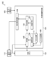
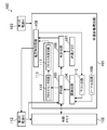
- FIG. 1 is a configuration diagram of a data interface system including a semiconductor integrated circuit according to the first embodiment.
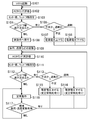
- FIG. 2 is a flowchart relating to voltage control of the semiconductor integrated circuit of FIG.
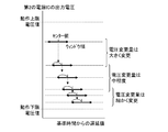
- FIG. 3 is a diagram illustrating the relationship among the delay value from the reference time, the power supply voltage, and the window in the determination circuit of FIG.
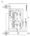
- FIG. 4 is a configuration diagram of a data interface system including a semiconductor integrated circuit according to the second embodiment.
- FIG. 5 is a configuration diagram of a data interface system including a semiconductor integrated circuit according to the third embodiment.
- FIG. 6 is a configuration diagram of a data interface system including a semiconductor integrated circuit according to the fourth embodiment.
- FIG. 1 is a configuration diagram of a data interface system including a semiconductor integrated circuit according to the first embodiment.
- the data interface system 100 includes a semiconductor integrated circuit 101, an external memory 102, a first power supply IC 103, and a second power supply IC 112.
- data is transmitted and received between the semiconductor integrated circuit 101 to which a voltage is supplied from the first power supply IC 103 and the external memory 102 to which a voltage is supplied from the second power supply IC 112.
- the semiconductor integrated circuit 101 includes an IF circuit 105, a determination circuit 106, a voltage control circuit 108, a test circuit 110, a normal circuit 109, an arbitration circuit 104, and a built-in memory 107 as a table circuit.
- the IF circuit 105 receives the voltage supplied from the second power supply IC 112 and operates. Specifically, the IF circuit 105 accesses the external memory 102 to read and write data.
- the test circuit 110 instructs the IF circuit 105 to execute an access test to the external memory 102 in accordance with the output timing from the voltage control circuit 108. As a result, the IF circuit 105 executes an access test on the external memory 102.
- the normal circuit 109 instructs the IF circuit 105 to perform normal access to the external memory 102 during actual operation of the data interface system 100.
- the arbitration circuit 104 arbitrates between an access test instruction from the test circuit 110 and a normal access instruction from the normal circuit 109. For example, during an actual operation of the data interface system 100, when the voltage control circuit 108 gives an instruction to start an access test to the test circuit 110, the arbitration circuit 104 relays the instruction from the test circuit 110 to the IF circuit 105. .
- the determination circuit 106 evaluates the AC timing between the external memory 102 and the IF circuit 105. Specifically, the determination circuit 106 determines the AC timing between the external memory 102 and the IF circuit 105 based on the access result of the IF circuit 105, that is, the result of the access test. Then, the determination circuit 106 generates control information for controlling the output voltage of the second power supply IC 112 based on the AC timing. For example, the determination circuit 106 compares the AC timing with a predetermined value stored in the built-in memory 107. If the AC timing is larger than the predetermined value, the determination circuit 106 may decrease the output voltage of the second power supply IC 112. Control information is generated. On the other hand, when the AC timing is smaller than a predetermined value, control information indicating that the output voltage of the second power supply IC 112 is increased is generated.
- the determination circuit 106 can be constituted by a variable delay element, for example. Then, by searching the write timing and the read timing for the external memory 102, a range (window) in which the data from the external memory 102 matches the expected value may be determined. Note that the configuration of the determination circuit 106 is arbitrary.
- the built-in memory 107 As predetermined values, for example, AC timing based on design information of the semiconductor integrated circuit 101 and control information indicating the value of the voltage to be output by the second power supply IC 112 are stored in association with each other. ing. Although details of the internal memory 107 will be described later, the internal memory 107 only needs to store information necessary for evaluating the AC timing.
- the voltage control circuit 108 controls the output voltage of the second power supply IC 112 according to the control information generated by the determination circuit 106. Further, the voltage control circuit 108 instructs the test circuit 110 to start an access test. That is, the output from the voltage control circuit 108 serves as a trigger for the AC timing to be evaluated by the determination circuit 106.
- circuits other than the IF circuit 105 operate with a voltage supplied from the first power supply IC 103.
- a voltage is supplied from the first power supply IC 103 to the semiconductor integrated circuit 101 to operate each circuit in the semiconductor integrated circuit 101, and the design of the semiconductor integrated circuit 101 is performed from the voltage control circuit 108 to the second power supply IC 112. Power supply voltage information based on the information is input. As a result, a voltage is supplied from the second power supply IC 112 to the external memory 102 and the IF circuit 105, and the system is activated (S101).
- the voltage control circuit 108 After starting the system, the voltage control circuit 108 issues a trigger for starting the AC timing evaluation to the test circuit 110.
- the AC timing is detected by the determination circuit 106, and the write timing or read timing is determined.
- the determination circuit 106 obtains information on the AC timing, such as the upper and lower limits of the window, the center value, and the delay value from the reference time.
- the delay value from the reference time is, for example, a time defined by a delay time based on the AC timing search start time.
- the data transmission / reception timing to the external memory 102 is set to be the center value of the window. Further, the window width is calculated from the upper limit value and the lower limit value of the window (S103).
- the minimum window width necessary for performing stable data transmission / reception is compared with the window width obtained in S103, and it is determined whether or not the window width is excessive or insufficient (S104).
- S104 the minimum window width necessary for data transmission / reception is stored in the built-in memory 107 in advance, and the information is compared with the AC timing obtained by the determination circuit 106.
- the control information indicating that the voltage of the second power supply IC 112 is lowered is output from the determination circuit 106 to the voltage control circuit 108, and the voltage control circuit is accordingly displayed. 108 lowers the voltage of the second power supply IC 112 (S106).
- the AC timing obtained by the determination circuit 106 is larger than the minimum required window width, stable data transmission / reception is possible, but in order to obtain the minimum required window width, the external memory 102 and the IF circuit Lower the power supply voltage to 105.
- control information indicating that the voltage of the second power supply IC 112 is increased is output from the determination circuit 106 to the voltage control circuit 108.
- the voltage control circuit 108 increases the voltage of the second power supply IC 112 (S107).
- the voltage control circuit 108 causes the external memory 102 and the IF circuit 105 to be transmitted.
- the window width can be increased by increasing the power supply voltage, and the window width necessary for stable data transmission / reception can be ensured.
- the process returns to S102, and the AC timing is re-evaluated. That is, after changing a certain power supply voltage, a trigger is issued from the voltage control circuit 108 to the test circuit 110.
- the excess or deficiency of the window width is resolved, the voltage output from the second power supply IC 112 is optimized, and the power consumption is reduced. Can be reduced.
- the data interface system 100 transitions to the actual operation state (S108). That is, normal access by the IF circuit 105 is performed in accordance with an instruction from the normal circuit 109.
- the load and temperature of the semiconductor integrated circuit 101 vary (S109). Due to this variation, there is a possibility that the window width of the AC timing is deviated from the reference value. Therefore, a trigger is issued again from the voltage control circuit 108 to the test circuit 110, and the AC timing is re-evaluated (S110).
- the center value and the window width are calculated from the AC timing during the actual operation of the data interface system 100 by re-evaluating the AC timing by the determination circuit 106 (S111). Further, the determination circuit 106 determines whether or not the window width is excessive or insufficient (S112).
- the control information indicating that the voltage of the second power supply IC 112 is lowered is output from the determination circuit 106 to the voltage control circuit 108, and the voltage control circuit is accordingly displayed. 108 lowers the voltage of the second power supply IC 112 (S114).
- control information indicating that the voltage of the second power supply IC 112 is increased is output from the determination circuit 106 to the voltage control circuit 108.
- the voltage control circuit 108 increases the voltage of the second power supply IC 112 (S115).
- the amount of change in the output voltage of the second power supply IC 112 by performing the AC timing evaluation once.
- the amount of change in the output voltage of the second power supply IC 112 is limited so that the window center value before the voltage change, that is, the data transmission / reception timing is within the window width after the voltage change.
- the output voltage of the second power supply IC 112 is decreased so that the center value before the voltage change is within the window width after the voltage change ( S114).
- the output voltage of the second power supply IC 112 is increased so that the center value before the voltage change is within the range of the window width after the voltage change ( S115).
- the voltage change amount of the second power supply IC 112 is set to be different between the system startup and the actual operation.
- the process returns to S110, and the above processing is repeated until the AC timing window width is eliminated. Accordingly, the output voltage of the second power supply IC 112 can be dynamically optimized, so that the power consumption of the semiconductor integrated circuit 101 can be reduced. Even if the second power supply IC 112 is dynamically controlled, the data interface system 100 can transmit and receive data normally.
- the data interface system 100 enters a steady operation state (S116).
- Changes in the data transmission / reception load and the temperature of the semiconductor integrated circuit 101 between the external memory 102 and the IF circuit 105 may affect the window width of the AC timing.
- the window width of the AC timing decreases due to power integrity and signal integrity, so that stable data transmission / reception with the external memory 102 becomes difficult.
- the temperature of the semiconductor integrated circuit 101 rises, the drive capability of the IF circuit 105 decreases, and the window width of the AC timing tends to decrease.
- the voltage control circuit 108 sends the A trigger is issued to perform an AC timing reevaluation.
- the arbitration circuit 104 preferentially executes the access test by the test circuit 110, whereby the AC timing is re-evaluated by the determination circuit 106 (S110). ).
- the window width of the AC timing is optimized. Therefore, the window width is maintained at a size necessary for data transmission / reception, and the output voltage of the second power supply IC 112 is kept to a minimum level even in a steady operation state, so that data transmission / reception is stabilized and low consumption is achieved. Electricity becomes possible.
- the output voltage of one power source (a power source corresponding to the first power IC 103) is controlled according to the internal load state of the semiconductor integrated circuit 101.
- the power supply voltage to the IF circuit 105 and the semiconductor integrated circuit 101 is dynamically controlled using the first and second power supply ICs 103 and 112. Since the internal load level of the semiconductor integrated circuit 101 and the load level of data transmission / reception of the external memory 102 and the IF circuit 105 often do not coincide with each other, in this embodiment, these circuits are separated from independent power supply ICs. An optimum voltage can be supplied.
- the center value before changing the output voltage of the second power supply IC 112 must be within the range of the window width after the voltage change.
- FIG. 3 is a diagram showing the relationship between the delay value from the reference time, the window upper limit value, the lower limit value, the center value, the window width, and the output voltage of the second power supply IC 112 in the determination circuit 106 of FIG. .
- the data transmission / reception load between the semiconductor integrated circuit 101 and the external memory 102 and the AC timing window width due to temperature fluctuations of the semiconductor integrated circuit 101 are eliminated, and the second power supply IC 112 After the output voltage converges, a relationship is obtained in which the AC timing window width is constant without depending on the output voltage.
- the amount of change in the output voltage may be fixed instead of being variable.
- the built-in memory 107 stores a window width value necessary for maintaining stable data transmission / reception between the semiconductor integrated circuit 101 and the external memory 102.
- the window width value is called by the determination circuit 106 every time AC timing is evaluated, and becomes a reference for comparison.
- the determination circuit 106 identifies an address in the built-in memory 107 that stores the window width corresponding to the window width obtained by the evaluation of the AC timing at the time of starting the system, and acquires an output voltage value corresponding to the address. To do.
- the determination circuit 106 calculates the difference between the output voltage value corresponding to the required window width and the current output voltage value, and outputs this difference value to the voltage control circuit 108 as control information.
- the voltage control circuit 108 changes the output voltage of the second power supply IC 112 according to the control information.
- the center of the window before changing the output voltage of the second power supply IC 112 in order to maintain normal data transmission / reception in the normal access between the external memory 102 and the IF circuit 105.
- the built-in memory 107 stores in advance a relationship between the output voltage of the second power supply IC 112 and the amount of change in the output voltage based on the delay value from the reference time, as shown in FIG.
- the change amount of the stored output voltage is set so that the center value of the data transmission / reception timing before changing the output voltage is within the range of the AC timing window after changing the output voltage.
- the determination circuit 106 Based on the delay value from the reference time obtained by the AC timing evaluation, the determination circuit 106 identifies an address in which the delay value from the corresponding reference time in the built-in memory 107 is stored, and uses the delay value as the delay value. Get the corresponding output voltage change amount.
- the determination circuit 106 outputs the acquired change amount to the voltage control circuit 108 as control information.
- the voltage control circuit 108 changes the output voltage of the second power supply IC 112 according to the control information from the determination circuit 106.
- the data stored in advance in the built-in memory 107 is not limited to data prepared in the process of manufacturing the semiconductor integrated circuit 101 based on the design information of the semiconductor integrated circuit 101.
- a system start-up or actual operation test may be performed, and an actual measurement value corresponding to each semiconductor integrated circuit 101 may be stored in the built-in memory 107 as data.
- the data in the built-in memory 107 may be set by trimming the pre-shipment inspection of the semiconductor integrated circuit 101 or by calibration at system startup.
- the determination circuit 106 reads the actual measurement data stored in the built-in memory 107, when the system is activated, the address where the window width information is stored is specified, and the corresponding output voltage value is acquired. Further, in actual operation, an address where the reference time is stored may be specified and a corresponding output voltage value may be acquired.
- the AC timing is evaluated at each voltage value while changing the output voltage of the second power supply IC 112
- the delay value from the reference time, Data on the upper limit value, lower limit value, center value, and window width of the window may be acquired, and these data may be stored in the built-in memory 107 as a table.
- the voltage supplied to the IF circuit 105 and the external memory 102 can be dynamically controlled based on the AC timing between the external memory 102 and the IF circuit 105. Therefore, the power consumption of the semiconductor integrated circuit 101 can be reduced while maintaining stable data transmission / reception between the external memory 102 and the IF circuit 105.
- the voltage is dynamically controlled based on the AC timing, it is possible to adjust the timing of data transmission / reception in units of clocks or less.
- the AC timing is evaluated when there is a load or temperature change. For example, a timer is provided, and the AC timing is evaluated every time a certain time elapses. You may make it do.
- FIG. 4 is a configuration diagram of a data interface system including a semiconductor integrated circuit according to the second embodiment. In the present embodiment, differences from the first embodiment will be mainly described.
- the temperature detector 111 monitors the temperature of the IF circuit 105, and outputs to the voltage control circuit 108 that the temperature of the IF circuit 105 has changed by a predetermined value or more based on the monitoring result of the temperature monitor circuit 113. And a temperature determination circuit 114.
- the temperature monitor circuit 113 monitors the temperature of the IF circuit 105 and outputs the temperature to the temperature determination circuit 114.
- the temperature determination circuit 114 stores the output of the temperature monitor circuit 113. For example, immediately after the actual operation, the temperature of the IF circuit 105 after system startup is stored.
- the temperature of the IF circuit 105 is output from the temperature monitor circuit 113 to the temperature determination circuit 114.
- the temperature determination circuit 114 notifies the voltage control circuit 108 of the change. Note that the temperature determination circuit 114 may notify when the temperature of the IF circuit 105 is a predetermined value.
- the voltage control circuit 108 issues a trigger to the test circuit 110 based on the output timing from the temperature determination circuit 114. That is, the voltage control circuit 108 instructs the test circuit 110 to start an access test.
- the AC timing is evaluated by the determination circuit 106, and the output voltage of the second power supply IC 112 is dynamically controlled. Therefore, even if the temperature of the semiconductor integrated circuit 101 changes, the window width is kept constant, so that stable data transmission / reception can be maintained.
- the temperature monitor circuit 113 monitors the temperature periodically or constantly, and the temperature determination circuit 114 detects that the temperature changes by a predetermined value or more. Alternatively, when the temperature is a predetermined value, the voltage control circuit 108 is notified. That is, the temperature detection unit 111 performs processing related to S109 and S117 shown in FIG.
- the present embodiment even when the data transmission / reception load between the external memory 102 and the IF circuit 105 is constant, when the temperature change of the semiconductor integrated circuit 101 occurs, the AC timing is re-evaluated, and the second The output voltage of the power supply IC 112 can be readjusted. Therefore, even if the temperature changes, the window width can be kept constant, and stable data transmission / reception between the external memory 102 and the IF circuit 105 can be ensured.
- FIG. 5 is a configuration diagram of a data interface system including a semiconductor integrated circuit according to the third embodiment. In the present embodiment, differences from the first embodiment will be mainly described.
- the semiconductor integrated circuit 101 in FIG. 5 includes a process detection unit 115 in addition to the configuration of the semiconductor integrated circuit 101 in FIG.
- the process detection unit 115 should output the process monitor circuit 116 that monitors individual manufacturing variations of the IF circuit 105 mounted on the semiconductor integrated circuit 101 and the second power supply IC 112 based on the monitoring result of the process monitor circuit 116. And a process determination circuit 117 for outputting voltage data.
- the process monitor circuit 116 monitors a physical quantity indicating the current capability of the transistor in the IF circuit 105. Further, the process determination circuit 117 determines whether or not the manufacturing variation of the IF circuit 105 is located within a predetermined standard based on the physical quantity.
- the process determination circuit 117 compares the monitoring result of the process monitor circuit 116 with the physical quantity that is a reference that is trimmed in the inspection before the shipment of the semiconductor integrated circuit 101, so that the physical quantity of the individual IF circuit 105 is determined. The deviation from the center value of the standard range can be determined.
- the process monitor circuit 116 monitors the manufacturing variation of the IF circuit 105 and outputs the monitoring result to the process determination circuit 117.
- the process determination circuit 117 receives the output of the process monitor circuit 116 and determines the deviation of the above-described physical quantity from the center value in a predetermined standard range. Then, the process determination circuit 117 converts the deviation amount into a voltage value, and outputs the converted voltage value to the voltage control circuit 108.
- the voltage control circuit 108 reflects the voltage value from the process determination circuit 117 on the output voltage of the second power supply IC 112.
- the semiconductor integrated circuit 101 Since the power supply voltage value at the time of starting the system varies depending on the manufacturing variation of each semiconductor integrated circuit 101, the semiconductor integrated circuit 101 is started with an appropriate voltage by taking into account the output of the process detection unit 115. be able to. Then, the flow after S102 shown in FIG. 3 is performed.
- the voltage control circuit 108 controls the output voltage of the second power supply IC 112 based on the change amount of the voltage based on the evaluation of the AC timing and the information obtained by converting the deviation amount from the process detection unit 115 into the voltage. As a result, the excess or deficiency of the window width is solved. The same applies after the transition to the actual operation state.
- the power supply voltage for each manufacturing variation of the semiconductor integrated circuit 101 it is not necessary to store the power supply voltage for each manufacturing variation of the semiconductor integrated circuit 101, the data related to the window width, the delay value from the reference time, and the like in the built-in memory 107.
- the capacity of the built-in memory 107 can be small.
- a suitable voltage change amount can be calculated for each individual having manufacturing variations using the data in the built-in memory 107.
- the monitor result of the process monitor circuit 116 is compared with the center value in the range of a predetermined standard, and when the current capability of the transistor in the IF circuit 105 is high, it is determined by trimming in the pre-shipment inspection. Information for reducing a certain amount of voltage is output to the voltage control circuit 108.
- FIG. 6 is a configuration diagram of a data interface system including a semiconductor integrated circuit according to the fourth embodiment. In the present embodiment, differences from the first embodiment will be mainly described.
- the voltage monitor circuit 118 monitors the voltage supplied from the second power supply IC 112 to the IF circuit 105 and informs the voltage control circuit 108 that this voltage has changed by a predetermined value or more, or that this voltage is a predetermined value. Output.
- the voltage monitor circuit 118 monitors the voltage supplied to the IF circuit 105 and stores the voltage value.
- the voltage supplied to the IF circuit 105 fluctuates. Therefore, when this voltage changes by a predetermined value or when this voltage is a predetermined value, The voltage monitor circuit 118 notifies the voltage control circuit 108 for evaluating the AC timing.
- the voltage control circuit 108 outputs a trigger to the test circuit 110 in accordance with the output timing of the voltage monitor circuit 118. Thereby, AC timing is evaluated.
- the fluctuation of the output voltage of the second power supply IC 112 can be regarded as the fluctuation of the load shown in S109 and S117 of FIG.
- the present embodiment by monitoring the voltage supplied to the IF circuit 105, it is possible to detect fluctuations in the data transmission / reception load between the external memory 102 and the IF circuit 105, re-evaluation of AC timing, and The output voltage of the second power supply IC 112 can be readjusted. Therefore, it is possible to ensure the stability of data transmission / reception between the external memory 102 and the IF circuit 105 while maintaining the window width of the AC timing constant.
- the data transmission / reception load between the external memory 102 and the IF circuit 105 is set as a trigger requirement for performing the reevaluation of the AC timing, but waiting for issuing an instruction to the arbitration circuit 104 (queue)
- the load of the IF circuit 105 may be determined by monitoring data patterns such as the data toggle rate of the IF circuit 105 and the data simultaneous change rate, and the result may be used as a trigger requirement. Further, the load of the IF circuit 105 may be monitored by a user program of the semiconductor integrated circuit 101, and the result may be used as a trigger requirement.
- a control circuit based on the AC timing may be generated by providing a memory in the determination circuit 106.
- the built-in memory 107 may be omitted.
- the semiconductor integrated circuit according to the present disclosure is useful for reducing power consumption of various systems that perform data communication because it can perform stable voltage transmission and reception while dynamically controlling voltage.
Landscapes
- Engineering & Computer Science (AREA)
- Theoretical Computer Science (AREA)
- Physics & Mathematics (AREA)
- General Physics & Mathematics (AREA)
- Power Engineering (AREA)
- General Engineering & Computer Science (AREA)
- Electromagnetism (AREA)
- Radar, Positioning & Navigation (AREA)
- Automation & Control Theory (AREA)
- Semiconductor Integrated Circuits (AREA)
- Power Sources (AREA)
- Computer Hardware Design (AREA)
Abstract
Description
図1は、第1の実施形態に係る半導体集積回路を備えたデータインタフェースシステムの構成図である。
図4は、第2の実施形態に係る半導体集積回路を備えたデータインタフェースシステムの構成図である。本実施形態では、主に、第1の実施形態との相違点について説明する。
図5は、第3の実施形態に係る半導体集積回路を備えたデータインタフェースシステムの構成図である。本実施形態では、主に、第1の実施形態との相違点について説明する。
図6は、第4の実施形態に係る半導体集積回路を備えたデータインタフェースシステムの構成図である。本実施形態では、主に、第1の実施形態との相違点について説明する。
101 半導体集積回路
102 外部メモリ
103 第1の電源IC
104 調停回路
105 IF回路(インタフェース回路)
106 判定回路
107 内蔵メモリ(テーブル回路)
108 電圧制御回路
109 ノーマル回路
110 テスト回路
111 温度検知部
112 第2の電源IC
115 プロセス検知部
118 電圧モニタ回路
Claims (11)
- 第1の電源IC(Integrated Circuit)から供給される電圧で動作し、外部メモリとデータの送受信を行う半導体集積回路であって、
前記第1の電源ICとは別の第2の電源ICから供給される電圧を受けて動作し、前記外部メモリにアクセスして、前記外部メモリとデータの送受信を行うインタフェース回路と、
前記インタフェース回路のアクセス結果に基づいて、前記外部メモリと前記インタフェース回路とのAC(Alternate Current)タイミングを判定し、当該ACタイミングに基づいて前記第2の電源ICの出力電圧を制御する制御情報を生成する判定回路と、
前記制御情報に従って、前記第2の電源ICの出力電圧を制御する電圧制御回路とを備えている
ことを特徴とする半導体集積回路。 - 請求項1の半導体集積回路において、
前記判定回路は、前記ACタイミングが所定値よりも大きい場合には、前記第2の電源ICの出力電圧を下げることを示す前記制御情報を生成する一方、前記ACタイミングが前記所定値よりも小さい場合には、前記第2の電源ICの出力電圧を上げることを示す前記制御情報を生成する
ことを特徴とする半導体集積回路。 - 請求項1の半導体集積回路において、
前記インタフェース回路に対して前記外部メモリへのアクセステストを実行するように指示するテスト回路と、
前記インタフェース回路に対して前記外部メモリへの通常アクセスを実行するように指示するノーマル回路と、
前記テスト回路による前記アクセステストの指示と前記ノーマル回路による前記通常アクセスの指示とを調停する調停回路とを備え、
前記電圧制御回路は、前記テスト回路に対して、前記アクセステストの開始を指示し、
前記判定回路は、前記アクセステストの結果によって得られた前記ACタイミングに基づいて前記制御情報を生成する
ことを特徴とする半導体集積回路。 - 請求項1の半導体集積回路において、
前記インタフェース回路の温度を検知し、当該温度が所定値以上変化したこと、あるいは当該温度が所定値であることを出力する温度検知部を備え、
前記電圧制御回路は、前記温度検知部からの出力タイミングに基づいて、前記第2の電源ICの出力電圧を制御する
ことを特徴とする半導体集積回路。 - 請求項1の半導体集積回路において、
前記インタフェース回路の単体固有の製造ばらつきを検知し、当該製造ばらつきに基づいて前記第2の電源ICが出力すべき電圧の情報を出力するプロセス検知部を備え、
前記電圧制御回路は、前記プロセス検知部の出力に基づいて、前記第2の電源ICの出力電圧を制御する
ことを特徴とする半導体集積回路。 - 請求項1の半導体集積回路において、
前記第2の電源ICから前記インタフェース回路に供給される電圧を検知し、当該電圧が所定値以上変化したこと、あるいは当該電圧が所定値であることを出力する電圧モニタ回路を備え、
前記電圧制御回路は、前記電圧モニタ回路からの出力タイミングに基づいて、前記第2の電源ICの出力電圧を制御する
ことを特徴とする半導体集積回路。 - 請求項1の半導体集積回路において、
前記第2の電源ICが出力すべき電圧の情報が格納されたテーブル回路を備え、
前記判定回路は、前記テーブル回路を参照して前記制御情報を生成する
ことを特徴とする半導体集積回路。 - 請求項7の半導体集積回路において、
前記テーブル回路には、前記第2の電源ICが出力すべき電圧の値と、前記インタフェース回路および前記外部メモリのデータの送受信が正常となるように設定されたACタイミングとが対応づけて格納されている
ことを特徴とする半導体集積回路。 - 請求項8の半導体集積回路において、
前記テーブル回路に格納されているACタイミングは、
前記電圧制御回路によって前記第2の電源ICの電圧が変更された後におけるACタイミングのセンター値が、前記第2の電源ICの電圧が変更される前におけるACタイミングの範囲内となるように設定されている
ことを特徴とする半導体集積回路。 - 請求項7乃至9のうちいずれか1つの半導体集積回路において、
前記テーブル回路に格納されるデータは、当該半導体集積回路の出荷前検査のトリミング、あるいは当該半導体集積回路の起動時のキャリブレーションにより設定される
ことを特徴とする半導体集積回路。 - 請求項1の半導体集積回路と、
前記第1の電源ICと、
前記第2の電源ICと、
前記第2の電源ICから電圧が供給される前記外部メモリとを備えている
ことを特徴とするデータインタフェースシステム。
Priority Applications (4)
| Application Number | Priority Date | Filing Date | Title |
|---|---|---|---|
| JP2015522482A JP6245262B2 (ja) | 2013-06-11 | 2014-03-31 | 半導体集積回路およびそれを備えたデータインタフェースシステム |
| CN201480030636.9A CN105283854B (zh) | 2013-06-11 | 2014-03-31 | 半导体集成电路及包括该半导体集成电路的数据接口系统 |
| US14/964,435 US10089258B2 (en) | 2013-06-11 | 2015-12-09 | Semiconductor integrated circuit, and data interface system provided with same, which provides for dynamic control of the supply voltage |
| US16/111,668 US10802997B2 (en) | 2013-06-11 | 2018-08-24 | Method for controlling power supply voltage in semiconductor integrated circuit |
Applications Claiming Priority (2)
| Application Number | Priority Date | Filing Date | Title |
|---|---|---|---|
| JP2013122327 | 2013-06-11 | ||
| JP2013-122327 | 2013-06-11 |
Related Child Applications (1)
| Application Number | Title | Priority Date | Filing Date |
|---|---|---|---|
| US14/964,435 Continuation US10089258B2 (en) | 2013-06-11 | 2015-12-09 | Semiconductor integrated circuit, and data interface system provided with same, which provides for dynamic control of the supply voltage |
Publications (1)
| Publication Number | Publication Date |
|---|---|
| WO2014199545A1 true WO2014199545A1 (ja) | 2014-12-18 |
Family
ID=52021872
Family Applications (1)
| Application Number | Title | Priority Date | Filing Date |
|---|---|---|---|
| PCT/JP2014/001890 Ceased WO2014199545A1 (ja) | 2013-06-11 | 2014-03-31 | 半導体集積回路およびそれを備えたデータインタフェースシステム |
Country Status (4)
| Country | Link |
|---|---|
| US (2) | US10089258B2 (ja) |
| JP (1) | JP6245262B2 (ja) |
| CN (2) | CN105283854B (ja) |
| WO (1) | WO2014199545A1 (ja) |
Families Citing this family (3)
| Publication number | Priority date | Publication date | Assignee | Title |
|---|---|---|---|---|
| WO2019082263A1 (ja) * | 2017-10-24 | 2019-05-02 | 株式会社ソシオネクスト | 変換器及びデータ転送システム |
| US11608737B2 (en) * | 2019-02-19 | 2023-03-21 | Geodynamics, Inc. | Valve status indicator system and method |
| CA3202924A1 (en) * | 2022-08-25 | 2024-02-25 | Weibin MA | Power supply voltage control method and apparatus, blockchain server, and storage medium |
Citations (3)
| Publication number | Priority date | Publication date | Assignee | Title |
|---|---|---|---|---|
| JP2002015599A (ja) * | 2000-06-27 | 2002-01-18 | Oki Electric Ind Co Ltd | 半導体記憶装置 |
| JP2007164970A (ja) * | 2005-12-09 | 2007-06-28 | A-Data Technology Co Ltd | 不揮発性メモリ装置及びそのコントローラ |
| JP2011003088A (ja) * | 2009-06-19 | 2011-01-06 | Panasonic Corp | データラッチ調整装置およびそれを用いたメモリアクセスシステム |
Family Cites Families (8)
| Publication number | Priority date | Publication date | Assignee | Title |
|---|---|---|---|---|
| US6757857B2 (en) * | 2001-04-10 | 2004-06-29 | International Business Machines Corporation | Alternating current built in self test (AC BIST) with variable data receiver voltage reference for performing high-speed AC memory subsystem self-test |
| CN1453853A (zh) * | 2002-04-27 | 2003-11-05 | 力旺电子股份有限公司 | 非易失性动态随机存取存储器 |
| US7236894B2 (en) * | 2004-12-23 | 2007-06-26 | Rambus Inc. | Circuits, systems and methods for dynamic reference voltage calibration |
| JP2008098774A (ja) * | 2006-10-06 | 2008-04-24 | Oki Electric Ind Co Ltd | 半導体集積回路装置 |
| JP4465539B2 (ja) | 2008-03-12 | 2010-05-19 | Okiセミコンダクタ株式会社 | メモリ制御装置及び方法 |
| WO2012131796A1 (ja) * | 2011-03-28 | 2012-10-04 | パナソニック株式会社 | メモリインターフェース回路およびメモリシステム |
| US9536626B2 (en) * | 2013-02-08 | 2017-01-03 | Intel Corporation | Memory subsystem I/O performance based on in-system empirical testing |
| US9461626B2 (en) * | 2014-07-14 | 2016-10-04 | Qualcomm Incorporated | Dynamic voltage adjustment of an I/O interface signal |
-
2014
- 2014-03-31 CN CN201480030636.9A patent/CN105283854B/zh active Active
- 2014-03-31 CN CN201910297052.2A patent/CN109947164B/zh active Active
- 2014-03-31 WO PCT/JP2014/001890 patent/WO2014199545A1/ja not_active Ceased
- 2014-03-31 JP JP2015522482A patent/JP6245262B2/ja active Active
-
2015
- 2015-12-09 US US14/964,435 patent/US10089258B2/en active Active
-
2018
- 2018-08-24 US US16/111,668 patent/US10802997B2/en active Active
Patent Citations (3)
| Publication number | Priority date | Publication date | Assignee | Title |
|---|---|---|---|---|
| JP2002015599A (ja) * | 2000-06-27 | 2002-01-18 | Oki Electric Ind Co Ltd | 半導体記憶装置 |
| JP2007164970A (ja) * | 2005-12-09 | 2007-06-28 | A-Data Technology Co Ltd | 不揮発性メモリ装置及びそのコントローラ |
| JP2011003088A (ja) * | 2009-06-19 | 2011-01-06 | Panasonic Corp | データラッチ調整装置およびそれを用いたメモリアクセスシステム |
Also Published As
| Publication number | Publication date |
|---|---|
| CN105283854A (zh) | 2016-01-27 |
| CN109947164B (zh) | 2020-10-09 |
| US10802997B2 (en) | 2020-10-13 |
| JP6245262B2 (ja) | 2017-12-13 |
| US10089258B2 (en) | 2018-10-02 |
| US20180365178A1 (en) | 2018-12-20 |
| US20160091943A1 (en) | 2016-03-31 |
| CN105283854B (zh) | 2019-05-07 |
| JPWO2014199545A1 (ja) | 2017-02-23 |
| CN109947164A (zh) | 2019-06-28 |
Similar Documents
| Publication | Publication Date | Title |
|---|---|---|
| US8442697B2 (en) | Method and apparatus for on-demand power management | |
| US10114390B2 (en) | Fan control system, computer system, and fan controlling method thereof | |
| US8954770B2 (en) | Controlling temperature of multiple domains of a multi-domain processor using a cross domain margin | |
| EP2635948B1 (en) | Method and apparatus for thermal control of processing nodes | |
| US9703336B2 (en) | System and method for thermal management in a multi-functional portable computing device | |
| US9411343B2 (en) | Temperature feedback control system for dynamic voltage frequency scaling | |
| US20130246820A1 (en) | Method for adaptive performance optimization of the soc | |
| US20150160716A1 (en) | Information processing apparatus, data transfer apparatus, and control method for data transfer apparatus | |
| JP2007233782A (ja) | 発熱量の制御方法およびコンピュータ | |
| JP2008026948A (ja) | 半導体集積回路 | |
| TW201339820A (zh) | 使用串列介面之適應性電壓比例調整 | |
| EP3036598B1 (en) | Power signal interface | |
| EP3274787B1 (en) | Technologies for managing power of an embedded controller during a low-power state | |
| KR20160085892A (ko) | 칩상의 시스템에서의 동작 주파수 조정 및 작업부하 스케쥴링을 위한 시스템 및 방법 | |
| JP6245262B2 (ja) | 半導体集積回路およびそれを備えたデータインタフェースシステム | |
| JP5956090B2 (ja) | 適応型電圧スケーリング(avs)を行うための方法およびavsを行うように構成された集積回路 | |
| JP2014052969A (ja) | クロック周波数制御装置、半導体装置 | |
| US10067483B1 (en) | Controlling electrical device based on temperature and voltage | |
| US9817743B2 (en) | Maintenance apparatus of electronic device, maintenance method of electronic device, and non-transitory computer readable medium storing program | |
| CN116400754A (zh) | 电子装置及电子装置中控制温度的方法 | |
| JP2015036965A (ja) | メモリ制御装置、メモリ制御装置の制御方法及び情報処理装置 | |
| JP6392743B2 (ja) | 制御回路および制御方法 | |
| US10318396B2 (en) | Technologies for temperature measurement of a processor | |
| CN117212215B (zh) | 一种风扇调速参数确定方法、装置、电子设备及存储介质 | |
| JP2012251944A (ja) | センサーモジュール |
Legal Events
| Date | Code | Title | Description |
|---|---|---|---|
| WWE | Wipo information: entry into national phase |
Ref document number: 201480030636.9 Country of ref document: CN |
|
| 121 | Ep: the epo has been informed by wipo that ep was designated in this application |
Ref document number: 14810642 Country of ref document: EP Kind code of ref document: A1 |
|
| ENP | Entry into the national phase |
Ref document number: 2015522482 Country of ref document: JP Kind code of ref document: A |
|
| NENP | Non-entry into the national phase |
Ref country code: DE |
|
| 122 | Ep: pct application non-entry in european phase |
Ref document number: 14810642 Country of ref document: EP Kind code of ref document: A1 |