WO2014196448A1 - 補償光学システムの調整方法、補償光学システム、及び補償光学システム用プログラムを記憶する記録媒体 - Google Patents
補償光学システムの調整方法、補償光学システム、及び補償光学システム用プログラムを記憶する記録媒体 Download PDFInfo
- Publication number
- WO2014196448A1 WO2014196448A1 PCT/JP2014/064294 JP2014064294W WO2014196448A1 WO 2014196448 A1 WO2014196448 A1 WO 2014196448A1 JP 2014064294 W JP2014064294 W JP 2014064294W WO 2014196448 A1 WO2014196448 A1 WO 2014196448A1
- Authority
- WO
- WIPO (PCT)
- Prior art keywords
- phase
- light intensity
- intensity distribution
- region
- wavefront
- Prior art date
- Legal status (The legal status is an assumption and is not a legal conclusion. Google has not performed a legal analysis and makes no representation as to the accuracy of the status listed.)
- Ceased
Links
Images














Classifications
-
- G—PHYSICS
- G02—OPTICS
- G02B—OPTICAL ELEMENTS, SYSTEMS OR APPARATUS
- G02B26/00—Optical devices or arrangements for the control of light using movable or deformable optical elements
- G02B26/06—Optical devices or arrangements for the control of light using movable or deformable optical elements for controlling the phase of light
-
- G—PHYSICS
- G01—MEASURING; TESTING
- G01J—MEASUREMENT OF INTENSITY, VELOCITY, SPECTRAL CONTENT, POLARISATION, PHASE OR PULSE CHARACTERISTICS OF INFRARED, VISIBLE OR ULTRAVIOLET LIGHT; COLORIMETRY; RADIATION PYROMETRY
- G01J9/00—Measuring optical phase difference; Determining degree of coherence; Measuring optical wavelength
-
- G—PHYSICS
- G01—MEASURING; TESTING
- G01M—TESTING STATIC OR DYNAMIC BALANCE OF MACHINES OR STRUCTURES; TESTING OF STRUCTURES OR APPARATUS, NOT OTHERWISE PROVIDED FOR
- G01M11/00—Testing of optical apparatus; Testing structures by optical methods not otherwise provided for
- G01M11/02—Testing optical properties
-
- G—PHYSICS
- G02—OPTICS
- G02B—OPTICAL ELEMENTS, SYSTEMS OR APPARATUS
- G02B27/00—Optical systems or apparatus not provided for by any of the groups G02B1/00 - G02B26/00, G02B30/00
- G02B27/0025—Optical systems or apparatus not provided for by any of the groups G02B1/00 - G02B26/00, G02B30/00 for optical correction, e.g. distorsion, aberration
- G02B27/0068—Optical systems or apparatus not provided for by any of the groups G02B1/00 - G02B26/00, G02B30/00 for optical correction, e.g. distorsion, aberration having means for controlling the degree of correction, e.g. using phase modulators, movable elements
-
- G—PHYSICS
- G02—OPTICS
- G02F—OPTICAL DEVICES OR ARRANGEMENTS FOR THE CONTROL OF LIGHT BY MODIFICATION OF THE OPTICAL PROPERTIES OF THE MEDIA OF THE ELEMENTS INVOLVED THEREIN; NON-LINEAR OPTICS; FREQUENCY-CHANGING OF LIGHT; OPTICAL LOGIC ELEMENTS; OPTICAL ANALOGUE/DIGITAL CONVERTERS
- G02F1/00—Devices or arrangements for the control of the intensity, colour, phase, polarisation or direction of light arriving from an independent light source, e.g. switching, gating or modulating; Non-linear optics
- G02F1/01—Devices or arrangements for the control of the intensity, colour, phase, polarisation or direction of light arriving from an independent light source, e.g. switching, gating or modulating; Non-linear optics for the control of the intensity, phase, polarisation or colour
- G02F1/13—Devices or arrangements for the control of the intensity, colour, phase, polarisation or direction of light arriving from an independent light source, e.g. switching, gating or modulating; Non-linear optics for the control of the intensity, phase, polarisation or colour based on liquid crystals, e.g. single liquid crystal display cells
-
- G—PHYSICS
- G02—OPTICS
- G02F—OPTICAL DEVICES OR ARRANGEMENTS FOR THE CONTROL OF LIGHT BY MODIFICATION OF THE OPTICAL PROPERTIES OF THE MEDIA OF THE ELEMENTS INVOLVED THEREIN; NON-LINEAR OPTICS; FREQUENCY-CHANGING OF LIGHT; OPTICAL LOGIC ELEMENTS; OPTICAL ANALOGUE/DIGITAL CONVERTERS
- G02F2203/00—Function characteristic
- G02F2203/18—Function characteristic adaptive optics, e.g. wavefront correction
Definitions
- One aspect of the present invention relates to a compensation optical system adjustment method, a compensation optical system, and a recording medium that stores a program for the compensation optical system.
- Non-Patent Documents 1 and 2 describe a method of adjusting an adaptive optical system by a phase measurement method.
- a phase measurement method a known phase distribution is displayed on a spatial light modulator, this phase distribution is measured by a wavefront sensor, and the measurement result is compared with the known phase distribution, thereby making it possible to measure the phase distribution on the modulation surface.
- the coordinates and the coordinates on the detection surface are associated with each other.
- the adaptive optics technology is a technology that dynamically removes aberrations by measuring optical aberration (wavefront distortion) using a wavefront sensor and controlling the wavefront modulation element (spatial light modulator) based on the result. is there.
- This adaptive optics technique it is possible to improve the imaging characteristics, the degree of light collection, the SN ratio of the image, and the measurement accuracy.
- adaptive optics technology has been mainly used in astronomical telescopes and large laser devices.
- adaptive optics technology is being applied to fundus cameras, scanning laser ophthalmoscopes, optical coherence tomographs, laser microscopes, and the like. Imaging using such an adaptive optics technique enables observation with an unprecedented high resolution.
- the adaptive optics system for realizing the adaptive optics technique as described above is mainly composed of a spatial light modulator, a wavefront sensor, and a control device for controlling them.
- adjustment (calibration) of the adaptive optics system is required.
- the calibration of the adaptive optics system is mainly to adjust the correspondence between the control signal to the spatial light modulator and the measurement signal from the wavefront sensor.
- the correspondence of (1) above can be easily obtained from the phase modulation characteristics of the spatial light modulator.
- the phase modulation characteristics of the spatial light modulator may depend on the environment (for example, temperature or change with time) in which the spatial light modulator is used, but in many cases it is negligible.
- the correspondence relationship (2) depends on the spatial positional relationship between the spatial light modulator and the wavefront sensor (mainly the positional relationship in the plane intersecting the optical axis).
- the wavefront is controlled with accuracy below the wavelength of light (for example, sub-micro level). Therefore, the phase distribution measured by the wavefront sensor and displayed on the spatial light modulator due to vibration at the time of transportation and installation, or deformation of the wavefront sensor and the member holding the spatial light modulator due to heat, etc. Misalignment may occur with the compensation phase pattern. Therefore, it is desirable that the adjustment work related to (2) be performed not only when the apparatus including the adaptive optical system is assembled and maintained, but also immediately before using the apparatus or between a plurality of imaging operations. Therefore, a means for easily and highly accurately executing the adjustment work described above is required.
- the accuracy of adjustment is the phase modulation accuracy of the spatial light modulator, the phase measurement of the wavefront sensor.
- the accuracy and the accuracy of the optical image for calibration it is difficult to stably realize high accuracy.
- One aspect of the present invention has been made in view of these problems.
- the correspondence relationship between the phase pattern measured by the wavefront sensor and the compensation phase pattern displayed on the spatial light modulator is short-time. It is another object of the present invention to provide a compensation optical system adjustment method that can be adjusted with high accuracy, a compensation optical system, and a recording medium that stores a program for the compensation optical system.
- an adjustment method for an adaptive optics system includes a spatial light modulator that spatially modulates the phase of an optical image incident on a modulation surface, and a plurality of lenses.
- a wavefront sensor having a lens array arranged in a dimension and a light detecting element for detecting a light intensity distribution including a condensing spot formed by the lens array and receiving a modulated light image from a spatial light modulator;
- a compensation optical system that compensates for wavefront distortion by controlling the phase pattern displayed on the spatial light modulator based on the wavefront shape of the optical image obtained from the light intensity distribution, the correspondence between the modulation surface and the wavefront sensor
- a method of adjusting the relationship wherein the first region on the modulation surface that is intended to correspond to one of a plurality of lenses or two or more adjacent lenses is linear in at least one direction
- One of the first phase pattern and the second phase pattern that is spatially nonlinear is displayed, and the other of the first and second phase patterns is displayed in
- the adaptive optical system adjustment method includes a second light intensity distribution acquisition step of acquiring a light intensity distribution by the light detection element in a state where spatially nonlinear phase patterns are displayed in the first and second regions. And a numerical value related to the clarity of the condensing spot included in the light intensity distribution obtained in the first light intensity distribution acquisition step, and the condensing included in the light intensity distribution obtained in the second light intensity distribution acquisition step.
- a difference calculation step of calculating a difference from a numerical value related to the clarity of the spot, and the clarity of the condensed spot included in the light intensity distribution obtained in the first light intensity distribution acquisition step during the adjustment step Instead, the correspondence between the modulation surface and the wavefront sensor may be adjusted based on the difference obtained in the difference calculation step.
- the adjustment of the correspondence relationship between the modulation surface and the wavefront sensor in the adjustment step includes the position coordinates and the wavefront assumed on the modulation surface when displaying the phase pattern for wavefront distortion compensation.
- the relative positional relationship with the sensor may be adjusted.
- the adjustment of the correspondence relationship between the modulation surface and the wavefront sensor in the adjustment step is an adjustment of the relative relationship between the attachment position of the wavefront sensor and the attachment position of the spatial light modulator. Also good.
- the width of the first region in the arrangement direction of the plurality of lenses is (n 1 / M) times the arrangement pitch of the plurality of lenses (where n 1 is a natural number, M May be the imaging magnification of the optical system between the modulation surface and the lens array.
- the adjustment method of the adaptive optical system includes a spatially nonlinear phase pattern (that is, a phase pattern having a spatially nonlinear phase profile), a random distribution in which the distribution of phase magnitudes is irregular, and a collection. It may include at least one of defocus distributions for expanding the diameter of the light spot.
- the adjustment method of the adaptive optics system is such that a phase pattern having linearity in at least one direction (that is, a phase pattern having linearity in at least one direction) has a substantially uniform phase distribution and tilted in at least one direction.
- Phase distribution a phase distribution having a cylindrical lens effect in the first direction and substantially uniform in a second direction intersecting (for example, orthogonal to) the first direction, and a diffraction grating in the first direction
- And may include at least one of phase distributions that are substantially uniform in a second direction that intersects (eg, is orthogonal to) the first direction.
- An adaptive optics system includes a spatial light modulator that spatially modulates the phase of an optical image incident on a modulation surface, a lens array in which a plurality of lenses are two-dimensionally arranged, and A wavefront sensor that has a light detecting element that detects a light intensity distribution including a condensing spot formed by a lens array and receives a modulated light image from a spatial light modulator, and a light image obtained from the light intensity distribution
- a control unit that compensates for wavefront distortion by controlling a phase pattern displayed on the spatial light modulator based on the wavefront shape, and the control unit is one of a plurality of lenses or two or more lenses adjacent to each other
- One of a first phase pattern having linearity in at least one direction and a spatially nonlinear second phase pattern is displayed in the first region on the modulation surface to be made to correspond to In a state where the other of the first and second phase patterns is displayed in the second region surrounding the region, the light intensity distribution is acquired by the light detection element, and
- the adaptive optics system program is formed by a spatial light modulator that spatially modulates the phase of an optical image incident on the modulation surface, a lens array in which a plurality of lenses are arranged two-dimensionally, and a lens array.
- a wavefront sensor having a light detecting element for detecting a light intensity distribution including a focused spot and receiving a modulated light image from a spatial light modulator, and a wavefront shape of the light image obtained from the light intensity distribution
- a compensation optical system comprising a control unit that compensates for wavefront distortion by controlling a phase pattern displayed on a spatial light modulator, and a program for controlling the operation of the control unit, comprising: A first phase pattern having a linearity in at least one direction and a spatial region in a first region on the modulation surface to be associated with one or two or more lenses adjacent to each other One of the non-linear second phase patterns is displayed, and the other of the first and second phase patterns is displayed in the second region surrounding the first region.
- the correspondence relationship between the modulation surface and the wavefront sensor And an adjustment step for adjusting the control unit.
- a recording medium for storing a program for an adaptive optics system includes a spatial light modulator that spatially modulates the phase of an optical image incident on a modulation surface, and a plurality of lenses in a two-dimensional shape.
- a wavefront sensor having an arrayed lens array, a light detecting element for detecting a light intensity distribution including a condensing spot formed by the lens array, receiving a modulated light image from a spatial light modulator, and a light intensity;
- an adaptive optics system comprising a controller that compensates for wavefront distortion by controlling a phase pattern displayed on a spatial light modulator based on a wavefront shape of an optical image obtained from the distribution, for controlling the operation of the controller
- the adaptive optics system program is a recording medium storing the adaptive optics system program, and the adaptive optics system program is one of a plurality of lenses or two or more lenses adjacent to each other.
- One of a first phase pattern having linearity in at least one direction and a spatially nonlinear second phase pattern is displayed in the first region on the modulation surface to be made to correspond to
- the phase pattern measured by the wavefront sensor is displayed on the spatial light modulator.
- the correspondence relationship with the compensation phase pattern can be adjusted in a short time and with high accuracy.
- FIG. 1 is a diagram schematically showing a configuration of an adaptive optics system according to an embodiment.
- FIG. It is sectional drawing which shows the structure of the wavefront sensor of one Embodiment roughly, Comprising: The cross section along the optical axis of the optical image is shown. It is the figure which looked at the lens array with which a wavefront sensor is provided from the optical axis direction of an optical image. It is the figure which looked at the image sensor with which a wavefront sensor is provided from the optical axis direction of an optical image.
- FIG. 2 is a cross-sectional view schematically showing an LCOS type spatial light modulator as an example of the spatial light modulator of one embodiment, showing a cross section along the optical axis of an optical image.
- phase pattern having linearity in at least one direction it is a diagram showing a phase distribution having a substantially uniform phase value over the entire modulation surface.
- block diagram which shows an example of an internal structure of a control part.
- flowchart which shows the operation
- FIG. 1 A phase distribution in which the phase value is inclined in the first direction (for example, the row direction) and the phase value is substantially uniform in the second direction (for example, the column direction) intersecting (for example, orthogonal to) the first direction.
- FIG. It is a figure which shows the phase distribution which a phase value inclines in both the 1st direction (for example, row direction) and the 2nd direction (for example, column direction).
- the phase distribution in the first direction has a cylindrical lens effect and the phase distribution has a substantially uniform phase value in the second direction.
- the phase distribution in the first direction forms a diffraction grating, and the phase distribution has a substantially uniform phase value in the second direction.
- combination pattern obtained by superimposition It is a figure which shows the modification of a lens array. It is a figure which shows the modification of each area
- phase distribution refers to two-dimensionally distributed phase values
- phase pattern refers to a phase distribution (two-dimensional phase value) coded based on a certain standard
- phase profile refers to a distribution of phase values along a certain direction (line) in the phase distribution.
- FIG. 1 is a diagram schematically showing a configuration of an adaptive optics system 10 according to the present embodiment.
- the adaptive optics system 10 is incorporated into, for example, an ophthalmic examination apparatus, a laser processing apparatus, a microscope apparatus, or an adaptive optics apparatus.
- the adaptive optics system 10 includes a spatial light modulator (SLM) 11, a wavefront sensor 12, a control unit 13, a beam splitter 14, relay lenses 15 and 16, and a control circuit unit 17.
- SLM spatial light modulator
- the spatial light modulator 11 receives the optical image La on the modulation surface 11a for displaying the phase pattern, modulates the wavefront shape of the optical image La, and outputs the result.
- the light image La incident on the spatial light modulator 11 is, for example, light emitted from a laser light source or a super luminescent diode (SLD), or reflected light, scattered light, fluorescence, or the like generated from an observation object irradiated with the light. is there.
- the wavefront sensor 12 includes information relating to the wavefront shape of the optical image La that has arrived from the spatial light modulator 11 (typically, which appears due to aberrations of the optical system and represents wavefront distortion, that is, wavefront deviation from the reference wavefront).
- the data S1 is provided to the control unit 13.
- the control unit 13 Based on the data S ⁇ b> 1 obtained from the wavefront sensor 12, the control unit 13 generates a control signal S ⁇ b> 2 for causing the spatial light modulator 11 to display an appropriate phase pattern.
- the control unit 13 includes an input unit that inputs data S1 from the wavefront sensor 12, an aberration calculation unit that calculates aberration from the data S1, a phase pattern calculation unit that calculates a phase pattern to be displayed on the spatial light modulator 11, and A signal generation unit that generates the control signal S2 according to the calculated phase pattern is included.
- the control circuit unit 17 receives the control signal S2 from the control unit 13 and applies a voltage V1 based on the control signal S2 to the plurality of electrodes of the spatial light modulator 11.
- the beam splitter 14 is disposed between the wavefront sensor 12 and the spatial light modulator 11 and branches the optical image La.
- the beam splitter 14 may be any of a polarization direction independent type, a polarization direction dependent type, or a wavelength dependent type (dichroic mirror) beam splitter.
- One light image La branched by the beam splitter 14 is sent to a light detection element 18 such as a CCD, a photomultiplier tube, or an avalanche photodiode.
- the light detection element 18 is incorporated in, for example, a scanning laser ophthalmoscope (SLO), an optical tomography apparatus (Optical Coherence Tomography: OCT), a fundus camera, a microscope, a telescope, or the like.
- SLO scanning laser ophthalmoscope
- OCT optical tomography apparatus
- the other optical image La branched by the beam splitter 14 enters the wavefront sensor 12.
- Relay lenses 15 and 16 are arranged side by side in the optical axis direction between the wavefront sensor 12 and the spatial light modulator 11. By these relay lenses 15 and 16, the wavefront sensor 12 and the spatial light modulator 11 are maintained in an optical conjugate relationship with each other.
- An optical imaging lens and / or a deflection mirror may be further disposed between the wavefront sensor 12 and the spatial light modulator 11.
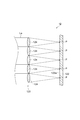
- FIG. 2 is a cross-sectional view schematically showing the configuration of the wavefront sensor 12 of the present embodiment, and shows a cross section along the optical axis of the optical image La.
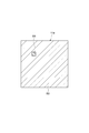
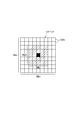
- FIG. 3 is a diagram of the lens array 120 included in the wavefront sensor 12 as viewed from the optical axis direction of the optical image La.
- FIG. 4 is a view of the image sensor (light detection element) 122 included in the wavefront sensor 12 as viewed from the optical axis direction of the optical image La.
- the wavefront sensor 12 includes an interference type and a non-interference type.
- a non-interference type Shack-Hartmann type wavefront sensor having a lens array 120 and an image sensor 122 is used as the wavefront sensor 12.
- the seismic resistance is superior to the case where an interference wavefront sensor is used, and the configuration of the wavefront sensor and the calculation processing of measurement data can be simplified. There is.
- the lens array 120 has N lenses (N is an integer of 4 or more).
- the N lenses 124 are arranged in a two-dimensional lattice pattern of Na rows and Nb columns (Na and Nb are integers of 2 or more).
- the image sensor 122 shown in FIG. 2 has a light receiving surface 122 a at a position overlapping the rear focal plane of the N lenses 124 constituting the lens array 120, and the N formed by the N lenses 124.
- a light intensity distribution including a single condensing spot P is detected.
- the image sensor 122 includes a plurality of pixels 122 b arranged in a two-dimensional grid of Ma rows and Mb columns (Ma and Mb are integers of 2 or more). Note that the row direction and column direction of the image sensor 122 coincide with the row direction and column direction of the lens array 120.
- the arrangement pitch of the pixels 122b of the image sensor 122 is sufficiently smaller than the arrangement pitch of the lenses 124 so that the magnitude of the deviation of the condensed image position from the reference position can be detected with high accuracy.
- the wavefront shape (phase gradient distribution) of the optical image La is measured based on the light intensity distribution detected by the image sensor 122. That is, the magnitude of the deviation between the position of the focused spot P by the lens 124 and the reference position is proportional to the local wavefront inclination of the optical image La incident on the lens 124. Therefore, the magnitude of the positional deviation of the condensed spot P from the reference position can be calculated for each lens 124, and the wavefront shape of the optical image La can be measured based on the positional deviation of the condensed spot P.
- the reference position used for calculating the magnitude of the deviation of the focused image position can be a position where the optical axis of each of the plurality of lenses 124 and the light receiving surface 122a of the image sensor 122 intersect. This position can be easily obtained by calculating the center of gravity using a condensed image obtained by allowing a parallel plane wave to vertically enter each lens 124.
- the spatial light modulator 11 is an element that receives a light image La from a light source or an observation object, modulates the wavefront of the light image La, and outputs the modulated light wave.
- the spatial light modulator 11 has a plurality of pixels (control points) arranged in a two-dimensional lattice, and modulates each pixel according to a control signal S2 provided from the control unit 13.
- the amount (for example, phase modulation amount) is changed.
- the spatial light modulator 11 includes, for example, LCOS-SLM (Liquid Crystal Crystal On Spatial Light Modulator), PPM (Programmable Phase Modulator), LCD (Liquid Crystal Display), micro electromechanical element (Micro Electro Electro Mechanical Systems; MEMS), or There is an electrical address type spatial light modulator formed by combining a liquid crystal display element and an optical address type liquid crystal spatial light modulator.
- LCOS-SLM Liquid Crystal Crystal On Spatial Light Modulator
- PPM Programmable Phase Modulator
- LCD Liquid Crystal Display
- MEMS Micro Electro Electro Electro Mechanical Systems
- an electrical address type spatial light modulator formed by combining a liquid crystal display element and an optical address type liquid crystal spatial light modulator.
- the reflective spatial light modulator 11 is shown in FIG. 1, the spatial light modulator 11 may be a transmissive type.
- FIG. 5 is a cross-sectional view schematically showing an LCOS type spatial light modulator as an example of the spatial light modulator 11 of the present embodiment, and shows a cross section along the optical axis of the optical image La.
- the spatial light modulator 11 includes a transparent substrate 111, a silicon substrate 112, a plurality of pixel electrodes 113, a liquid crystal part (modulation part) 114, a transparent electrode 115, alignment films 116a and 116b, a dielectric mirror 117, and a spacer 118. ing.
- the transparent substrate 111 is made of a material that transmits the optical image La, and is disposed along the main surface of the silicon substrate 112.
- the plurality of pixel electrodes 113 are arranged in a two-dimensional lattice pattern on the main surface of the silicon substrate 112 and constitute each pixel of the spatial light modulator 11.
- the transparent electrode 115 is disposed on the surface of the transparent substrate 111 facing the plurality of pixel electrodes 113.
- the liquid crystal unit 114 is disposed between the plurality of pixel electrodes 113 and the transparent electrode 115.
- the alignment film 116 a is disposed between the liquid crystal part 114 and the transparent electrode 115, and the alignment film 116 b is disposed between the liquid crystal part 114 and the plurality of pixel electrodes 113.
- the dielectric mirror 117 is disposed between the alignment film 116 b and the plurality of pixel electrodes 113.
- the dielectric mirror 117 reflects the light image La incident from the transparent substrate 111 and transmitted through the liquid crystal unit 114 and emits the light from the transparent substrate 111 again.
- the spatial light modulator 11 further includes a pixel electrode circuit (active matrix drive circuit) 119 that controls a voltage applied between the plurality of pixel electrodes 113 and the transparent electrode 115.
- a pixel electrode circuit active matrix drive circuit
- the liquid crystal unit 114 on the pixel electrode 113 is changed according to the magnitude of the electric field generated between the pixel electrode 113 and the transparent electrode 115.
- the refractive index of. Therefore, the optical path length of the optical image La that passes through the portion of the liquid crystal unit 114 changes, and as a result, the phase of the optical image La changes.
- the spatial distribution of the phase modulation amount can be electrically written, and various wavefront shapes can be realized as necessary. it can.
- FIG. 6 is a front view of the modulation surface 11 a of the spatial light modulator 11.
- the modulation surface 11 a includes a plurality of pixels 11 b arranged in a two-dimensional lattice pattern with Pa rows and Pb columns (Pa and Pb are integers of 2 or more).
- Each of the plurality of pixels 11b includes a plurality of pixel electrodes 113.
- a light image La from a light source (not shown) or an observation object enters the spatial light modulator 11 as substantially parallel light.
- the light image La modulated by the spatial light modulator 11 enters the beam splitter 14 via the relay lenses 15 and 16, and is branched into two light images.
- One optical image La after branching enters the wavefront sensor 12.
- the wavefront sensor 12 generates data S1 including the wavefront shape (phase distribution) of the optical image La, and the data S1 is provided to the control unit 13.
- the control unit 13 calculates the wavefront shape (phase distribution) of the optical image La as necessary based on the data S1 from the wavefront sensor 12, and calculates a phase pattern for appropriately compensating for the wavefront distortion of the optical image La.
- the control signal S2 including the signal is output to the spatial light modulator 11. Thereafter, the undistorted optical image La compensated by the spatial light modulator 11 is branched by the beam splitter 14, enters the light detection element 18 through an optical system (not shown), and is imaged.
- the coordinate systems on the modulation surface 11a of the spatial light modulator 11 and the detection surface of the wavefront sensor 12 are set as follows. That is, two directions parallel to and perpendicular to the modulation surface 11a of the spatial light modulator 11 are defined as an x-axis direction and a y-axis direction on the modulation surface 11a, and are parallel to the detection surface of the wavefront sensor 12 and to each other. Two orthogonal directions are defined as an x-axis direction and a y-axis direction on the detection surface.
- the x-axis on the modulation surface 11 a of the spatial light modulator 11 and the x-axis on the detection surface of the wavefront sensor 12 are opposite to each other, the y-axis on the modulation surface 11 a of the spatial light modulator 11, and the wavefront sensor 12. Are opposite to each other in the y-axis on the detection surface.
- the coordinates with the origin at the center of the modulation surface 11a of the spatial light modulator 11 are (Xs, Ys)
- the coordinates with the center of the detection surface of the wavefront sensor 12 at the origin are (Xc, Yc).
- Equation (1) M is the magnification of the relay lenses 15 and 16.
- (Xs 0 , Ys 0 ) are coordinates on the modulation surface 11 a of the spatial light modulator 11 projected onto the coordinate origin on the detection surface of the wavefront sensor 12, and the positions of the modulation surface 11 a and the detection surface. Indicates the amount of deviation. Note that the magnification M included in Equation (1) is often known.
- the adjustment (calibration) of the correspondence relationship between the modulation surface 11a and the wavefront sensor 12 of the adaptive optics system 10 in the present embodiment is performed by examining the values of (Xs 0 , Ys 0 ) and bringing these values close to zero. is there. In other words, the relative relationship between the mounting position of the wavefront sensor 12 and the mounting position of the spatial light modulator 11 is adjusted.
- the adjustment (calibration) of the correspondence relationship between the modulation surface 11a and the wavefront sensor 12 is performed when the phase pattern given to the spatial light modulator 11 and the wavefront shape obtained from the wavefront sensor 12 are associated with each other (Xs 0 , Ys 0 ). In other words, the relative positional relationship between the position coordinates assumed on the modulation surface 11 a and the wavefront sensor 12 when displaying the phase pattern for wavefront distortion compensation is adjusted.
- a special phase pattern for adjustment is displayed on the spatial light modulator 11, and the wavefront sensor 12 detects a characteristic caused by the phase pattern, thereby detecting the wavefront sensor 12.
- the positional deviation amount between the wavefront shape measured in step S1 and the phase pattern displayed on the spatial light modulator 11 is acquired, and the correspondence between the modulation surface 11a and the wavefront sensor 12 is adjusted (calibration) based on the positional deviation amount. ).
- This adjustment method is stored as a program in the storage area 13a of the control unit 13 shown in FIG. 1, and is performed by the control unit 13 reading and executing this program.
- FIG. 7 is a conceptual diagram for explaining the principle of the adjustment method in the present embodiment.
- the wavefronts W1 and W1 of the optical image incident on the modulation surface 11a the relay lenses 15 and 16
- the wavefront W2 of the optical image emitted from the modulation surface 11a and the wavefront W3 of the optical image incident on the wavefront sensor 12 are shown.
- the spatial light modulator 11 emits a wavefront W2 in which a wavefront corresponding to the phase pattern displayed on the spatial light modulator 11 is added to the incident wavefront W1.
- FIG. 7 shows an optical image La that is emitted from a region on the modulation surface 11 a corresponding to one lens 124 and reaches the lens 124.
- FIG. 8 is a diagram conceptually showing a special phase pattern displayed on the modulation surface 11a.
- a first phase pattern having linearity in at least one direction is displayed in a region B1 (hereinafter referred to as a first region) on the modulation surface 11a having a size corresponding to one lens 124.
- a first phase pattern is realized by including, for example, a substantially uniform phase distribution, a phase distribution inclined in at least one direction, and the like.
- such a first phase pattern has a cylindrical lens effect in a certain first direction, and a phase distribution that is substantially uniform in a second direction that intersects (eg, is orthogonal to) the first direction.
- the diffraction grating in the first direction and including a phase distribution that is substantially uniform in the second direction intersecting (for example, orthogonal to) the first direction.
- the substantially uniform phase distribution may be a phase distribution having a linear function.
- a spatially nonlinear second phase pattern (for example, having a phase magnitude) is formed in a region B2 (hereinafter referred to as a second region) surrounding the first region B1 on the modulation surface 11a.
- a random distribution with an irregular distribution, a defocus distribution for expanding the diameter of the focused spot, etc.) are displayed.
- the wavefront corresponding to the second region B2 in the outgoing wavefront W2 is disturbed (portion A1 in FIG. 7).
- the disturbance of the wavefront also occurs in the portion of the incident wavefront W3 incident on the wavefront sensor 12 that enters the lens 124 corresponding to the second region B2 (portion A2 in FIG. 7).
- the condensing spot P formed by the lens 124 is diffused, and the condensing spot P is not formed, or the light intensity is weak.
- the wavefront is disturbed in at least one direction due to the first phase pattern having linearity in at least one direction.
- the light enters the lens 124 without being processed. Therefore, the condensing spot P is clearly formed by the lens 124.
- FIG. 9 is a diagram conceptually showing light intensity distribution data (Shack-Hartmanngram) detected by the image sensor 122 of the wavefront sensor 12.
- FIG. 9A shows a light intensity distribution in the case where a phase pattern having linearity in at least one direction is displayed in the first region B1 and a spatially nonlinear phase pattern is displayed in the second region B2. Data D1 is shown.
- FIG. 9B shows light intensity distribution data D2 when a phase pattern having linearity is displayed in all regions.
- N focused spots P corresponding to the N lenses 124 are light intensity distribution data.
- N focused spots P corresponding to the N lenses 124 are light intensity distribution data.
- FIG. 9A a phase pattern having linearity in at least one direction is displayed in the first region B1, and a spatially nonlinear phase pattern is displayed in the second region B2.
- one focused spot P corresponding to the first area B1 is included in the light intensity distribution data, but the focused spot corresponding to the second area B2 is not formed or is a spot.
- the maximum brightness is reduced, or the spot diameter is widened. In other words, only the condensing spot corresponding to the second region B2 can be formed with reduced clarity.
- the adjustment (calibration) of the positional deviation between the phase pattern displayed on the spatial light modulator 11 and the wavefront shape measured by the wavefront sensor 12 is performed. Assuming that this is done properly.
- the case where these have a position shift is considered.
- FIG. 10A and 10 (b) are enlarged views showing the vicinity of the wavefront sensor 12 of FIG.
- FIG. 10A when the positional deviation adjustment between the phase pattern of the wavefront sensor 12 and the spatial light modulator 11 is appropriately performed, the wavefront portion A4 corresponding to the first region B1.
- the lens 124 corresponding to the first region B1 are completely coincident with each other when viewed from the optical axis direction. ) Is formed.
- the surrounding lens 124 that is, the lens 124 corresponding to the second region B2
- a condensing spot is not formed or becomes minute.
- the first when there is a positional deviation between the phase pattern of the wavefront sensor 12 and the spatial light modulator 11, the first is seen from the optical axis direction.
- the wavefront portion A4 corresponding to the region B1 overlaps the lens 124 corresponding to the first region B1 and another lens 124 adjacent to the lens 124.
- the light condensing spot P formed by the lens 124 corresponding to the first region B1 has a light intensity that is less clear than the case shown in FIG.
- such an optical image is referred to as a partially condensed image).
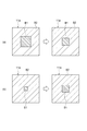
- FIG. 11A to FIG. 11C are plan views showing the positional relationship between the wavefront portion A4 and the lens 124 as seen from the optical axis direction in a simplified manner.
- the wavefront portion A4 is shown superimposed on the four lenses 124 adjacent to each other.
- the light intensity distribution data D1 includes four lenses as shown in FIG. 11D.
- Four condensing spots P each formed by 124 are included. If the center of the wavefront portion A4 is further brought closer to the center of a certain lens 124 from this state (FIG. 11 (b)), as shown in FIG. 11 (e), the other three lenses 124 and the wavefront portion A4.
- the condensing spot P formed by the other three lenses 124 becomes gradually weaker.
- the center of the wavefront portion A4 and the center of the lens 124 completely coincide with each other (FIG. 11C), as shown in FIG. 11F, the condensed light formed by the other three lenses 124.
- the spot P disappears or becomes extremely weak.
- the condensing spot P is formed as a total condensing point image.
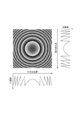
- phase pattern displayed in the second region B2 of FIG. FIG. 12 to FIG. 15 are diagrams showing examples of such phase patterns, where the magnitude of the phase is shown by light and dark, the phase of the darkest part is 0 (rad), and the brightest part is shown.
- the phase is 2 ⁇ (rad).
- FIG. 12 shows a random distribution in which the phase size distribution is irregular.
- FIG. 12 also illustrates a graph of the phase modulation amount profile at one location in each of the row direction and the column direction.
- FIG. 13 shows a defocus distribution in which the focused spot P is enlarged.
- FIG. 13 also illustrates a graph of the amount of phase modulation at one place in each of the row direction and the column direction.
- FIG. 14 shows a distribution that causes a large spherical aberration in the optical image La.
- a phase pattern that causes defocusing and spherical aberration a phase pattern that causes large astigmatism or coma may be used.
- FIG. 15 shows a distribution that causes an aberration including high-order aberrations of orders greater than spherical aberration, astigmatism, and coma aberration in the optical image La. Even when the phase pattern shown in FIGS. 14 and 15 is displayed in the second region B2, a clear focused spot P is not formed.
- the spatially nonlinear phase pattern may include at least one of these distributions, or may include a combined pattern obtained by superimposing at least one of these distributions and a linear phase pattern.
- the non-linear phase pattern displayed in the second area B2 may include a common phase distribution for each of a plurality of areas obtained by dividing the second area B2, and the second area B2 is divided. Different phase distributions may be included for each of the plurality of regions.
- FIG. 16 illustrates a phase pattern in which a common phase distribution (for example, a phase distribution including high-order aberrations) is arranged for each of a plurality of regions obtained by dividing the second region B2.
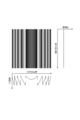
- FIG. 17 illustrates a phase pattern in which different phase distributions (for example, defocus distribution) are arranged for each of a plurality of regions obtained by dividing the second region B2.
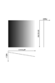
- the “phase pattern having linearity in at least one direction” displayed in the first region B1 in FIG. 8 is realized by, for example, a phase distribution having a substantially uniform phase value over the entire modulation surface 11a.
- FIG. 18 is a diagram showing such a phase pattern, and the magnitude of the phase is shown by light and dark as in FIGS.
- the phase pattern as shown in FIG. 18 is displayed in the first region B1
- the wavefront of the optical image La in the portion becomes flat, and thus a clear condensing spot P is formed by the lens 124.
- FIG. 19 is a block diagram illustrating an example of the internal configuration of the control unit 13 of the present embodiment.
- the control unit 13 can include a pattern creation unit 13b and a calculation processing unit 13c.
- the pattern creation unit 13b and the calculation processing unit 13c are stored as programs in the storage area 13a of the control unit 13 shown in FIG. 1, and are realized by the control unit 13 reading and executing this program. .
- the pattern creating unit 13b creates a special phase pattern for adjusting (calibrating) the correspondence between the modulation surface 11a and the wavefront sensor 12, that is, a phase pattern including the first region B1 and the second region B2. .
- the pattern creating unit 13b creates a phase pattern whose entire region is spatially nonlinear. These phase patterns are sent from the pattern creating unit 13b to the control circuit unit 17 as a control signal S2.
- a special phase pattern P A for calibration is represented by, for example, the following equation (2).
- a is a certain constant and is an example of a first phase pattern having linearity in at least one direction.
- rand () is a random function and is an example of a second phase pattern that is spatially nonlinear.
- N, m represents coordinates in pixel units on the modulation surface 11a.
- ROI is defined as a symbol representing the first region B1.
- the phase pattern P B in which the entire region is spatially nonlinear is represented by the following formula (3).
- the first region B1 in the present embodiment has a size corresponding to one lens 124.
- the shape of the first region B1 is a square. Therefore, the previous equation (2) can be modified as the following equation (4).
- (xc, yc) is the center coordinate of the first area B1
- w is the number of pixels on one side of the first area B1.
- the arrangement pitch of the pixels 11b on the modulation surface 11a is slmPITCH
- the arrangement pitch of the lenses 124 on the lens array 120 is mlaPITCH
- the imaging magnification of the optical system between the modulation surface 11a and the lens surface of the lens array 120 is M.
- the number of pixels w on one side of the first region B1 is expressed by the following formula (5).
- the calculation processing unit 13c acquires the light intensity distribution data S1 output from the wavefront sensor 12 when the phase patterns P A and P B described above are displayed on the modulation surface 11a.
- the calculation processing unit 13c calculates a feature amount related to the focused spot P included in the light intensity distribution data S1 according to an algorithm described later.
- the calculation processing unit 13c sets the first amount so that the feature amount satisfies the condition (typically, the feature amount is minimized or the feature amount is less than a predetermined threshold).
- the center position (xc, yc) of the region B1 is moved.
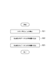
- FIG. 20 is a flowchart showing the operation of the adaptive optics system 10 of this embodiment and the correspondence adjustment method.
- the correspondence adjustment method is stored in the storage area 13a of the control unit 13 shown in FIG. 1 as an adaptive optics system program, and the control unit 13 reads and executes this program.
- the control unit 13 may be configured mainly by a computer including a CPU, a RAM and a ROM that are main storage devices, a communication module for performing communication, and hardware resources such as an auxiliary storage device such as a hard disk.
- the adaptive optics system program is stored in a recording medium that is inserted into the computer and accessed, or a recording medium provided in the computer.
- a recording medium include a magnetic disk, an optical disk, a CD-ROM, a USB memory, and a memory (storage area 13a) built in the computer.
- step S11 an initial process of the control unit 13 is performed (step S11).
- this initial processing step S11 for example, a memory area necessary for calculation processing is secured, initial parameter settings, and the like are performed.
- the initialization of the special phase pattern P A for calibration, the center of the first area B1 may be specified for any pixel in the vicinity of the center of the modulation surface 11a.
- the number of repetitions of subsequent steps S12 to S19 is set. The number of repetitions is set to an integer larger than a value obtained by squaring the number of pixels on one side in the first region B1, for example.
- the control unit 13 creates a special phase pattern P A for calibration, is displayed on the modulation surface 11a (step S12).
- a phase pattern having linearity in at least one direction (for example, the figure) is formed in the first region B1 on the modulation surface 11a to be associated with one lens 124 among the plurality of lenses 124 of the lens array 120. 18), and a spatially nonlinear phase pattern (see, for example, FIGS. 12 to 15) is displayed in the second region B2 surrounding the first region B1.
- step S13 First light intensity distribution acquisition step
- control unit 13 creates a phase pattern P B in which the entire region is spatially nonlinear, and displays the phase pattern P B on the modulation surface 11a (step S14).
- a spatially nonlinear phase pattern (see, for example, FIGS. 12 to 15) is displayed in both the first area B1 and the second area B2.
- step S15 Second light intensity distribution acquisition step
- control unit 13 obtains the figures for clarity of the light intensity distribution data D figures for clarity of Included focused spot P to A, and the light intensity distribution data D converged spot P contained in B (step S16).
- a numerical value related to the clarity of the focused spot P is referred to as a “feature amount”.
- feature amount a numerical value related to the clarity of the focused spot P.
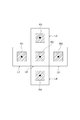
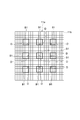
- FIG. 21 is a diagram showing a rectangular region L0 facing one lens 124 on the image sensor 122 and rectangular regions L1 to L4 facing four lenses 124 adjacent to the periphery of the lens 124. is there.
- regions L1 and L2 are aligned in the row direction with the region L0 interposed therebetween
- regions L3 and L4 are aligned in the column direction with the region L0 interposed therebetween.
- the number of pixels on one side of the regions L1 to L4 and the center distance (number of pixels) d between the regions L1 to L4 and the region L0 are expressed by the following equation (from the lens array pitch mlaPITCH and the image sensor image pitch ccdPITCH 6).
- feature amount calculation areas R0 to R4 are set inside the areas L0 to L4.
- the feature amount calculation regions R0 to R4 are similar to the regions L1 to L4, for example, and their center positions coincide with the center positions of the regions L1 to L4, respectively.
- FIG. 22 is an enlarged view of the regions L0 to L4.
- Each of the regions L0 to L4 is composed of a plurality of pixels 122b, and the plurality of pixels 122b are arranged in a two-dimensional lattice form over Ma 1 row and Mb 1 column (Ma 1 and Mb 1 are integers of 2 or more).
- the feature amount calculation regions R0 to R4 included in the regions L0 to L4 are indicated by parallel oblique lines in the drawing, and Ma 2 rows and Mb 2 columns (Ma 2 ⁇ Ma 1 , Mb 2 ⁇ Mb 1 ).
- the pixels 122b are arranged in a two-dimensional lattice pattern.
- the pixels painted out in black in the figure represent central pixels common to the regions L0 to L4 and the feature amount calculation regions R0 to R4.
- FIG. 23 is a flowchart showing a method of calculating the feature amount of the focused spot P.
- it detects the position of the condensing spot P in the light intensity distribution data D A (step S21).
- the position (c x , c y ) of the focused spot P is expressed by the following formula (7).
- a ij is the light intensity at the coordinates (i, j) of the light intensity distribution data D A
- R 0 is a feature amount calculation area including the peak position of the focused spot P.
- the center coordinates of the regions L0 and R0 are (c x , c y ) and expressed.
- the center coordinates of the regions L1 and R1 are (c x -d, c y ), the center coordinates of the regions L2 and R2 are (c x + d, c y ), and the center coordinates of the regions L3 and R3 are (c x , c y ⁇ d), the center coordinates of the regions L4 and R4 are represented as (c x , c y + d).
- the feature quantity calculation region R1 ⁇ R4 in the light intensity distribution data D B the feature quantity V B1 represented by the following formula (9), V B2, V B3, and calculates a V B4 (step S23) .
- the feature amounts V A1 to V A4 of the focused spot P included in the light intensity distribution data D A and the feature amounts V B1 to V B4 of the focused spot P included in the light intensity distribution data D B are calculated.
- the feature amount calculation formulas (8) and (9) regarding the clarity of the focused spot calculation is performed using the light intensity distribution data DA and DB, but the data after image processing of the light intensity distribution data DA and DB is performed. May be used to calculate.
- the calculated feature amount indicates the spread of the focused spot. That is, the feature amount related to the clarity of the focused spot includes an amount related to the power of the focused spot and an amount related to the spread of the focused spot.
- step S18 first, values V x and V y shown in the following equation (11) are calculated.
- the value V x is the absolute value of the difference between the difference ⁇ V 1 and the difference ⁇ V 2, and indicates the balance of the clarity of the focused spot P in the regions L1 and L2 arranged in the row direction across the region L0.
- the value V y is an absolute value of the difference between the difference ⁇ V 3 and the difference ⁇ V 4, and indicates the balance of the clarity of the focused spot P in the regions L3 and L4 arranged in the column direction across the region L0. .
- a direction value V x and the value V y is decreased to adjust the correspondence between the modulation surface 11a and the wavefront sensor 12.
- the difference ⁇ V 1 becomes smaller (or larger) than the difference ⁇ V 2
- the difference ⁇ V 1 becomes larger and the difference ⁇ V 2 becomes smaller (or the difference ⁇ V 1 becomes smaller and the difference ⁇ V 2 becomes larger).
- the difference ⁇ V 3 is smaller (or larger) than the difference ⁇ V 4
- the difference ⁇ V 3 becomes larger and the difference ⁇ V 4 becomes smaller (or the difference ⁇ V 3 becomes smaller and the difference ⁇ V 4 becomes larger).
- step S19 the control unit 13 determines whether or not the above differences ⁇ V 1 to ⁇ V 4 satisfy a predetermined end condition (step S19). For example, the control unit 13 determines whether the values V x and V y are minimum or whether the values V x and V y are below a predetermined threshold. When determining the end condition so that the values V x and V y are minimized, the above steps S12 to S19 are repeated until a preset number of repetitions is reached. Since the present embodiment moves the first region B1 of the phase pattern P A pixel by pixel, the maximum number of iterations is equal to the number of pixels constituting the first region B1. When determining the end condition based on the magnitudes of the values V x and V y and the predetermined threshold, steps S12 to S19 described above are repeated until the end condition is satisfied.
- the calibration is completed.
- the control unit 13 modifies the modulation surface 11a before the calibration described above.
- the wavefront sensor 12 may be adjusted (second adjustment step). For example, the relative relationship between the mounting position of the wavefront sensor 12 and the mounting position of the spatial light modulator 11 is adjusted so that the relative position between the phase pattern for compensating wavefront distortion and the wavefront sensor 12 matches each other.
- a phase pattern having linearity in at least one direction is displayed in the first region B1 of the spatial light modulator 11, and the first region B1 is surrounded. in a state of spatially display the nonlinear phase pattern in the second region B2, and acquires a light intensity distribution data D a by the image sensor 122 of the wavefront sensor 12.
- the condensing spot P in the region L0 is not clearly formed, and a part of the light from the first region B1 is condensed in any of the regions L1 to L4 via the adjacent lens 124. Further, the condensing spots P formed in the regions L1 to L4 become clear as the positional deviation increases. Accordingly, the correspondence between the modulation surface 11a and the wavefront sensor 12 can be adjusted based on the clarity of the focused spot P in the regions L0 to L4 (that is, the feature amounts V A1 to V A4 ).
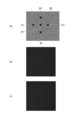
- FIG. 24 shows, as an example, (a) a special phase pattern for calibration, and (b) a light intensity distribution in a case where the first region B1 and the corresponding lens 124 are displaced.
- Data D A and (c) light intensity distribution data D A after calibration of the lens 124 corresponding to the first region B1 are shown.
- a plurality of first regions B1 (five locations in the figure) are provided.
- FIG. 24B when the positional deviation occurs, the focused spot P is dispersed and lacks clarity (FIG. 24B), but after calibration, the focused spot P is concentrated at one point. It can be seen that the clarity is increased (FIG. 24C).
- the calibration can be performed only by the phase pattern control of the spatial light modulator 11 by the control unit 13 and the calculation inside the control unit 13, and therefore the wavefront sensor 12 measures the calibration.
- the correspondence between the phase pattern and the compensation phase pattern displayed on the spatial light modulator 11 can be adjusted in a short time and with high accuracy.
- FIG. 25 is a diagram for explaining an advantage due to high accuracy of adjustment (calibration) of the adaptive optical system.
- FIG. 25A conceptually shows the incident wavefront 61, the compensation wavefront 62, and the compensated wavefront 63 (the sum of the incident wavefront 61 and the compensation wavefront 62) when the adjustment accuracy is low.
- FIG. 25B conceptually shows the incident wavefront 71, the compensation wavefront 72, and the compensated wavefront 73 (the sum of the incident wavefront 71 and the compensation wavefront 72) when the adjustment accuracy is high.
- the adjustment accuracy is low, if there is a positional shift between the incident wavefront 61 and the compensating wavefront 62, the wavefront distortion is not completely removed in the compensated wavefront 63. Accordingly, there is a possibility that the imaging characteristics are deteriorated, and the wavefront distortion may be increased due to the influence of feedback control.
- the adjustment accuracy is high and the positional deviation between the incident wavefront 71 and the compensation wavefront 72 is small, the wavefront distortion is appropriately corrected and the compensated wavefront 73 is obtained. Can be almost a plane wave.
- the structure of the phase pattern used for calibration is complicated, and the spatial light modulator 11 can accurately generate the structure of the complicated phase pattern. It's not easy.
- the present embodiment may be the first and second regions B1, B2 consist of a simple phase pattern including the phase pattern P A, the structure of the phase pattern is simple, the phase pattern by the control unit 13 Is easy and can be generated accurately.
- Non-Patent Document 2 it is necessary to calculate the overall wavefront shape based on the light intensity distribution data output from the wavefront sensor 12.
- calibration can be performed based on only a part of the light intensity distribution data, which facilitates calculation processing.
- Non-Patent Document 2 since it is desired that the phase pattern used for calibration is displayed on almost the entire modulation surface, a beam diameter of an optical image irradiated on the modulation surface is desired. A big thing is needed.
- the beam diameter of the optical image La may be at least three times the diameter of the lens 124.
- the beam diameter of the optical image La can be reduced, the size of the light source can be reduced. This makes it possible to perform the calibration work more easily.
- the modulation surface 11a and the wavefront sensor 12 are optically conjugate with each other, but if there is a deviation in their optical distance, the phase pattern displayed on the modulation surface 11a and the wavefront sensor 12 detect it. There is a difference between the phase pattern to be generated. Therefore, in the method described in Non-Patent Document 2, there is a concern about a decrease in calibration accuracy due to a shift in the optical distance between the modulation surface 11a and the wavefront sensor 12.
- the calibration accuracy can be maintained even when the modulation surface 11a and the wavefront sensor 12 are slightly deviated from the conjugate positional relationship.
- the reason is as follows.
- the modulation surface 11a and the wavefront sensor 12 are slightly deviated from a conjugate positional relationship, when the phase pattern of the first region B1 and the second region B2 is projected onto the wavefront sensor 12, it corresponds to the first region B1.
- the wavefront shape is a spherical wave obtained by adding some defocus components to the linear pattern, and the wavefront shape corresponding to the second region B2 is still a nonlinear (for example, random waveform) wavefront.
- the correspondence between the modulation surface 11a and the wavefront sensor 12 is preferably adjusted based on the differences ⁇ V 1 to ⁇ V 4 .
- the width of the wavefront portion A4 corresponding to the first region B1 matches the diameter of the lens 124, so that the condensing spot P in the region L0 shown in FIG. 21 and the converging spots in the surrounding regions L1 to L4. Since the difference in clarity with the light spot P can be emphasized, calibration can be performed with higher accuracy.
- the width of the first region B1 may be (n 1 / M) times (n 1 is an integer of 1 or more) times the arrangement pitch mlaPITCH of the plurality of lenses 124. Even in this case, the same effects as described above can be obtained.
- the present embodiment obtains the light intensity distribution data D A in a state of displaying a special phase pattern P A for calibration (step S13), and then the phase pattern P entire area is spatially non-linear It has acquired light intensity distribution data D B in a state of displaying the B (step S15).
- the light intensity distribution data D A, acquisition order of D B is not particularly limited, may acquire the light intensity distribution data D A after obtaining the light intensity distribution data D B.
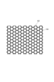
- a spatial light modulator in which a plurality of regular hexagonal pixels are arranged without gaps may be used.
- the spatial light modulator using liquid crystal has been described as an example.
- the spatial light modulator using a material having an electro-optic effect other than liquid crystal, or the pixel is formed by a micromirror.
- a spatial light modulator or a variable mirror that deforms a film mirror with an actuator may be used.
- step S13 it acquires the light intensity distribution data D A in a state of displaying the phase pattern P A (step S13), and after obtaining the light intensity distribution data D B while viewing the phase pattern P B (step In step S15, differences ⁇ V 1 to ⁇ V 4 between the feature amounts V A1 to V A4 and the feature amounts V B1 to V B4 calculated from the light intensity distribution data D A and D B are obtained.
- step S15 differences ⁇ V 1 to ⁇ V 4 between the feature amounts V A1 to V A4 and the feature amounts V B1 to V B4 calculated from the light intensity distribution data D A and D B are obtained.
- FIG. 26 is a flowchart showing an adjustment method (operation of the control unit 13) of the adaptive optics system 10 according to this modification.
- the control unit 13 performs steps S11 to S13 (see FIG. 20) similar to those in the above embodiment. Thereafter, Steps S14 and S15 shown in FIG. 20 are omitted, and the process proceeds to Step S36 for feature amount calculation.
- Step S36 is different from step S16 in the above embodiment in that step S21 (calculation of the spot centroid) and step S22 (calculation of feature amounts V A1 to V A4 ) shown in FIG. 23 are performed, and step S23 (feature) The calculation of the amounts V B1 to V B4 is omitted.
- control part 13 performs 1st adjustment step S37, without performing step S17 of the said embodiment.
- step S37 on the basis of the feature quantity V A1 ⁇ V A4 obtained in step S36, the control unit 13, the first region B1 of the phase pattern P A, to adjust the correspondence between the area L0.
- step S37 first, values V x and V y shown in the following equation (12) are calculated.
- the value V x is the absolute value of the difference between the feature value V A1 and the feature value V A2, and indicates the balance of clarity of the focused spot P in the regions L1 and L2 arranged in the row direction across the region L0.
- the value V y is the absolute value of the difference between the feature value V A3 and the feature value V A4, and indicates the balance of the clarity of the focused spot P in the regions L3 and L4 arranged in the column direction across the region L0. ing.
- a direction value V x and the value V y is decreased to adjust the correspondence between the modulation surface 11a and the wavefront sensor 12.
- the feature amount V A1 is larger (or smaller) than the feature amount V A2
- the feature amount V A1 increases and the feature amount V A2 decreases (or the feature amount V A1 decreases and the feature amount V A2 decreases).
- the direction of A2 increases), is moved by one pixel for example, the first area B1 in the row direction of the phase pattern P a.
- the feature amount V A3 is larger (or smaller) than the feature amount V A4
- the feature amount V A3 increases and the feature amount V A4 decreases (or the feature amount V A3 decreases and the feature amount V A4 decreases).
- the direction of A4 is increased), is moved by one pixel for example, the first area B1 in the column direction of the phase pattern P a.
- the control unit 13 determines whether or not the above-described feature amounts V A1 to V A4 satisfy a predetermined end condition (step S38). For example, the control unit 13 determines whether the values V x and V y are minimum or whether the values V x and V y are below a predetermined threshold. When determining the end condition so that the values V x and V y are minimized, the above-described steps S12 to 19 or S12 to S38 are repeated until a preset number of repetitions is reached. When determining the end condition based on the values V x and V y and the predetermined threshold value, the above-described steps S12 to S19 or S12 to S38 are repeated until the end condition is satisfied.
- the control unit 13 may adjust the correspondence between the modulation surface 11a and the wavefront sensor 12 (second adjustment step).
- the adjustment method in the second adjustment step is the same as in the above embodiment.
- the feature amounts V A1 to V A4 and the feature amounts V B1 to V B4 are calculated for the regions L1 to L4 adjacent to the region L0, and these feature amounts are calculated. Perform calibration based on However, calibration may be performed based on the feature amount for the region L0.
- the control unit 13 based on the difference [Delta] V 0 obtained in the difference calculation step S17, the control unit 13, the first region B1 of the phase pattern P A, the correspondence between the area L0 adjustment To do. More specifically, in the direction of the difference [Delta] V 0 increases, it is moved by the first one pixel, for example, in a row or column direction of the area B1 of the phase pattern P A.
- step S19 the control unit 13 determines whether or not the difference ⁇ V 0 satisfies a predetermined end condition. For example, the control unit 13 determines whether the difference ⁇ V 0 is maximum or whether the difference ⁇ V 0 exceeds a predetermined threshold. When determining the end condition so that the difference ⁇ V 0 is maximized, steps S12 to S19 are repeated until a preset number of repetitions is reached. When determining the end condition based on the difference ⁇ V 0 and the predetermined threshold, steps S12 to S19 are repeated until the end condition is satisfied.
- the process (second adjustment step) when the difference ⁇ V 0 satisfies a predetermined end condition is the same as that in the above embodiment.
- the correspondence relationship between the modulation surface 11 a and the wavefront sensor 12 is adjusted based on the difference ⁇ V 0 .
- the correspondence between the wavefront measured by the wavefront sensor 12 and the compensation phase pattern displayed on the spatial light modulator 11 can be increased in a short time.
- the accuracy can be adjusted.
- the correspondence may be adjusted based on the feature value V A0 instead of the difference ⁇ V 0 . In that case, since the number of steps is small, the time required for adjustment can be shortened. In the present modification, it is desirable that the light intensity of the light image La incident on the modulation surface 11a is constant over time.
- a first area B1 row direction (or column of the phase pattern P A In the direction) by one pixel when adjusting the correspondence between the modulation surface 11a and the wavefront sensor 12 in step S18 shown in FIG. 20, a first area B1 row direction (or column of the phase pattern P A In the direction) by one pixel.
- the movement amount of the first region B1 in step S18 is not limited to one pixel.
- the amount of movement of the first region B1 when the value V x is smaller than a predetermined value, the amount of movement of the first area B1 per time is one pixel, and when the value V x is larger than the predetermined value, the first area per time
- the amount of movement of B1 can be 2 pixels or 3 pixels.
- the relationship between the magnitudes of the values V x and V y (or the difference ⁇ V 0 ) and the amount of movement per movement of the first region B1 can be determined, for example, by an experiment performed in advance. In this experiment, for example, it is assumed that the wavefront sensor 12 and the spatial light modulator 11 are in an appropriate correspondence relationship, and the first region B1 is moved pixel by pixel in the row direction or the column direction from that state. Calculate the amount. Then, a graph showing the correlation between the movement amount (number of pixels) of the first region B1 and the values V x and V y (or the difference ⁇ V 0 ) is created. Based on this graph, the amount of movement per time of the first region B1 can be determined from the magnitudes of the values V x and V y (or the difference ⁇ V 0 ).
- the correspondence between the wavefront measured by the wavefront sensor 12 and the compensation phase pattern displayed on the spatial light modulator 11 can be obtained in a short time and with high accuracy. Can be adjusted. Further, by changing the movement amount of the first region B1 according to the magnitudes of the values V x and V y (or the difference ⁇ V 0 ), the time required for adjusting the correspondence can be shortened.
- the size of the first region B1 is set so that the size of the wavefront portion A4 (see FIG. 7) matches the diameter of one lens 124 (formula ( See 5)).
- the size of the first region B1 is not limited to this, and may be set to various sizes as shown below.
- FIG. 27 is a diagram illustrating examples of various sizes of the first region B1.
- 27A and 27B show the case where the size of the first region B1 is set so that the length (number of pixels) of one side of the region L0 is twice the diameter of the lens 124. Is shown conceptually.
- FIG. 27A shows a case where the length (number of pixels) of one side of the surrounding areas L1 to L4 is set to be equal to the diameter of the lens 124.
- the length of the side in contact with the region L0 (number of pixels) is equal to the length of the side of the region L0
- the length of the side not in contact with the region L0 is the diameter of the lens 124. Is set to be equal to.
- FIG. 27C conceptually shows a case where the size of the first region B1 is set so that the length (number of pixels) of one side of the region L0 is three times the diameter of the lens 124. Show. In the figure, the case where the length (number of pixels) of one side of the surrounding regions L1 to L4 is set to be equal to the diameter of the lens 124 is shown. However, as shown in FIG. The length of the side (the number of pixels) in contact with may be set to be equal to the length of the side of the region L0.
- FIG. 27D shows an example in which the length in the row direction and the length in the column direction of the first region B1 are different from each other.
- the length in the row direction and the length in the column direction of the region L0 are different from each other.
- the shapes of the surrounding regions L1 to L4 can be arbitrarily combined with the shape shown in FIG. 27A, the shape shown in FIG.
- the shape of the first region B1 according to this modification can be expressed as follows. That is, the arrangement pitch of the pixels 11b on the modulation surface 11a is slmPITCH, the arrangement pitch of the lenses 124 on the lens array 120 is mlaPITCH, and the imaging magnification of the optical system between the modulation surface 11a and the lens surface of the lens array 120 is M. Then, the number of pixels w on one side of the first region B1 is expressed by the following formula (15). However, n 1 is a natural number.
- step S12 shown in FIG. 20 the first phase pattern having linearity in at least one direction is displayed in the first region B1, and the spatially nonlinear second phase is displayed.
- the phase pattern is displayed in the second area B2.
- Equation (2) described above can be rewritten as follows.
- equation (3) can be rewritten as follows.
- a ′ is a certain constant and is an example of a first phase pattern having linearity in at least one direction.
- the correspondence relationship between the modulation surface 11a and the wavefront sensor 12 can be adjusted in the direction in which the values V x and V y decrease, as in step S18 shown in FIG.
- the correspondence between the wavefront measured by the wavefront sensor 12 and the compensation phase pattern displayed on the spatial light modulator 11 can be obtained in a short time and with high accuracy. Can be adjusted. Further, since a phase pattern having linearity can be displayed in all areas other than the first area B1, calibration is performed in parallel during execution of adaptive optics by using the phase pattern as a phase pattern for wavefront distortion compensation. Can be performed.
- the first phase pattern having linearity in at least one direction displayed in the first area B1 (second area B2 in the fifth modification)
- a constant a Or the substantially uniform distribution represented by a '
- the first phase pattern may be a phase distribution inclined (linearly changed) in at least one direction.
- a special phase pattern PA for calibration including such a phase pattern is expressed by the following formula (18).
- n 0 and m 0 are central pixels of the first region B 1 (ROI)
- a, b, and c are constants.
- the phase value is inclined in the first direction (for example, the row direction), and the phase value is substantially uniform in the second direction (for example, the column direction) intersecting (for example, orthogonal to) the first direction.
- FIG. 29 shows a phase distribution in which the phase value is inclined in both the first direction (for example, the row direction) and the second direction (for example, the column direction). This is the phase distribution in the ROI when b ⁇ 0 and c ⁇ 0 in the above equation (18). Note that FIGS. 28 and 29 also show graphs of phase modulation amounts in one row and one column in the row direction and the column direction, respectively.
- phase patterns When these phase patterns are displayed in the first area B 1, the wavefront of the optical image La in that portion becomes flat, and thus a clear focused spot P is formed by the lens 124. Therefore, calibration can be performed based on the clarity of the focused spot P in the regions L0 to L4, as in the above embodiment and each modification.
- the center of gravity of the focused spot P formed in the regions L0 to L4 is the center position of the regions L0 to L4 (ie, on the optical axis of each lens 124) by the inclination of the first phase pattern. ). Therefore, when calculating the feature amount, it is possible to perform the same calculation as in the above embodiment after moving the feature amount calculation regions R0 to R4 shown in FIG. 21 by the shift amount.
- the amount of deviation of the center of gravity position of the focused spot P is uniquely determined based on the configuration parameters of the wavefront sensor 12 and the coefficients b and c. Further, since the original center position can be obtained by subtracting the deviation amount from the gravity center position of the focused spot P, calibration can be performed by the same procedure as in the above embodiment.
- the first phase pattern displayed in the first region B1 (second region B2 in the fifth modification) has a cylindrical phase distribution in the first direction (for example, the row direction) as shown in FIG.
- the phase distribution may have a lens effect and the phase value may be substantially uniform in the second direction (for example, the column direction).
- a special phase pattern PA for calibration including such a phase distribution is expressed by the following equation (19).
- the phase value in the row direction is a substantially uniform, the phase distribution in the column direction has a cylindrical lens effect, the phase pattern P A in the case of constituting the phase distribution with a quadratic function, the following equation (20) Is represented by In the above formulas (19) and (20), n 0 and m 0 are central pixels of the first region B1 (ROI), and a 1 , b 1 , and c 1 are constants.
- phase pattern P A shown in Equation (19) When the phase pattern P A shown in Equation (19) is displayed on the modulation surface 11a, the wavefront sensor 12, extending in the row direction, converged spot P, which is focused in the column direction is formed. Thus, by using the phase pattern P A shown in Equation (19) can be carried out in the column direction calibration. Further, when the phase pattern P A shown in Equation (20) is displayed on the modulation surface 11a, the wavefront sensor 12, and focused in the row direction, converged spot P diffused in the column direction is formed. Therefore, it is possible by using the phase pattern P A shown in Equation (20), calibration is performed in the row direction. In this modification, for example, to calibrate the column direction by using the phase pattern P A shown in Equation (19), before or after, the row direction using a phase pattern P A shown in equation (20) Calibration can be performed.
- the first phase pattern displayed in the first region B1 (second region B2 in the fifth modification) has a diffracted phase distribution in the first direction (for example, the row direction) as shown in FIG. It may be a phase distribution that constitutes a grating and has a substantially uniform phase value in the second direction (for example, the column direction).
- phase pattern P A comprising a first phase pattern shown in Figure 31
- the wavefront sensor 12 a plurality of focused spots P separated in the row direction is formed.
- the phase pattern P A comprising a first phase pattern shown in Figure 31
- the modulation surface 11a is a row direction
- the modulation surface 11a can be displayed.
- the first phase pattern displayed in the first area B1 (second area B2 in the fifth modification) is a composite obtained by superimposing the phase distributions shown in the above embodiment and the seventh to ninth modifications on each other.
- a pattern may be included.
- FIG. 32 is a diagram showing an example of a composite pattern obtained by such superposition.
- the phase pattern shown in FIG. 32 (a) is the one shown in FIG. 30, and the phase pattern shown in FIG. 32 (b) is the one obtained by rotating the phase pattern shown in FIG. 28 by 90 °. .
- the phase pattern shown in FIG. 32C is a composite pattern in which these are superimposed.
- phase pattern P A comprising a synthetic pattern shown in FIG. 32 (c)
- the wavefront sensor 12 is diffused in the row direction, the focused spot P, which is focused in a column direction forming Is done.
- the phase pattern P A it is possible to perform column calibration.
- the phase pattern P A containing the synthetic patterns of the second direction is the row direction as the first phase pattern, modulation surface 11a can be displayed.
- a random distribution (FIG. 12) is used as an example of the spatially nonlinear second phase pattern displayed in the second region B2 (the first region B1 in the fifth modification).
- a defocus distribution (FIG. 13).
- the second phase pattern is not limited to these, and it is sufficient that the second phase pattern has a phase distribution such that a clear focused spot P is not formed.
- An example of such a phase distribution is a Fresnel Zone Plate (FZP) type phase pattern.
- the FZP type phase pattern has a function of condensing or diverging an incident light image La having a substantially uniform phase value.
- the position of the condensing spot P in the optical axis direction deviates from the focal plane of the lens 124 (that is, the surface of the image sensor 122). . For this reason, a blurred point image is formed on the surface of the image sensor 122.
- a special phase pattern PA for calibration including such an FZP type phase pattern is expressed by the following equation (21).
- a 2 are constants
- b 2 is sufficiently large constant.
- (N k , m k ) is the central pixel of the second region B2. Since b 2 is sufficiently large, the condensing spot P formed by the lens 124 can be sufficiently separated from the focal plane of the lens 124 (the surface of the image sensor 122).
- the lens array 120 of the wavefront sensor 12 is shown by FIG. 3, the form with which the some lens 124 was arranged in the two-dimensional lattice form is illustrated.
- the lens array of the wavefront sensor 12 is not limited to such a form.
- the lens array 120 may have a honeycomb structure in which a plurality of regular hexagonal lenses 128 are arranged without gaps.
- the first region B1 may be set to a hexagon.
- the region L0 and the like and the feature amount calculation region R0 and the like shown in FIG. 21 may all be set in a hexagon as shown in FIG.
- the values corresponding to the values V x and V y calculated in step S18 in FIG. 20 are the areas facing each other across the area L0 (specifically, the areas L1 and L2, the areas L3 and L4, and the area L5). And the feature amount calculated in L6).
- FIG. 35 is an enlarged view showing the vicinity of the wavefront sensor 12 of FIG.
- FIG. 35A shows a case where the width of the wavefront portion A4 corresponding to the first region B1 is slightly larger than the diameter of one lens 124
- FIG. 35B shows the width of the wavefront portion A4. The case where it is a little smaller than the diameter of one lens 124 is shown.
- the width of the wavefront portion A4 is slightly larger than the diameter of one lens 124, even if the center position of the wavefront portion A4 is close to the center of the lens 124, they are adjacent to each other. Since the amount of light incident on the lens 124 changes according to the positional deviation of the wavefront portion A4, the value V x (or value V y ) in the above embodiment varies. Therefore, as in the above embodiment, the end determination is performed based on whether the values V x and V y are the minimum or the values V x and V y are below a predetermined threshold value. High calibration accuracy can be maintained. On the other hand, as shown in FIG.
- the center position of the wavefront portion A4 is close to the center of the lens 124 in any of the cases shown in FIGS. 35 (a) and 35 (b). Since the amount of light incident on the lens 124 does not change according to the positional deviation of the wavefront portion A4, the calibration accuracy is slightly lowered as compared with the above embodiment.
- n 1 when n 1 is not a natural number, n 1 may be larger than 1.
- the end determination can be made based on whether the values V x and V y are minimum or the values V x and V y are below a predetermined threshold as in the above embodiment.
- Such a form is useful, for example, when the imaging magnification M between the spatial light modulator 11 and the wavefront sensor 12 has an error with respect to the design value.
- the numerical value estimated by Expression 5 (Expression 15) is also effective when it is a non-integer.
- an integer larger than the numerical value may be used as the width (number of pixels) of the first region B1.
- steps S12 ⁇ S18 following form can also be It is. That is, before performing calibration, by performing steps S12 to S18, a plurality of sets of values V x and V y (for example, the same number as the number of pixels constituting the first region B1) are acquired in advance. Keep it. At the time of calibration, steps S12 to S18 (until calculation of the values V x and V y ) are performed only once, and the obtained values V x and V y and a plurality of values V x and V acquired in advance are obtained. Compare the V y set.
- the maximum value of the displacement width between the first region B1 and the lens 124 corresponding to the first region B1 is ⁇ 1 of the number of pixels w on one side of the first region B1. / 2 times. Therefore, the number of combinations of positional relationships between the first region B1 and the lens 124 corresponding to the first region B1 is w ⁇ w. Of the w ⁇ w positional relationships, there is only one way in which the position of the first region B1 and the position of the lens 124 completely match, and the other (w ⁇ w ⁇ 1) ways. In this case, the first region B1 has a specific shift amount for each positional relationship in the row direction, the column direction, or both with respect to the lens 124.
- step S12 shown in FIG. 20 a plurality (typically w ⁇ w) of first regions B1 having different amounts of deviation from the corresponding lenses 124 by one pixel are obtained. create a phase pattern P a for calibration comprising simultaneously displaying the phase pattern P a on the modulation surface 11a.
- the arrangement pitch (number of pixels) of the first region B1 may be set to (2 ⁇ w) or more.
- the correspondence relationship between the modulation surface 11a and the wavefront sensor 12 is adjusted based on the shift amount of the first region B1 having the smallest values V x and V y calculated in step S18.
- calibration can be performed in a short time without repeating steps S12 to S18 shown in FIG.
- the (i, j) th center position of the first area B1 that is included in the phase pattern P A in this modification is represented by, for example, by the following equation (22).
- i ⁇ w / 2
- W / 2-1 and j ⁇ w / 2
- Pa is the number of pixels in the row direction of the modulation surface 11a
- Pb is the number of pixels in the column direction of the modulation surface 11a.
- the above equation (22) represents a case where the width of the wavefront portion A4 corresponding to the first region B1 and the diameter of the lens 124 are equal to each other (see equation (5)).
- a region indicated by a thick frame represents the first region B1
- one pixel D existing in each first region B1 is a pixel corresponding to the center of the corresponding lens 124.
- the center position of the first region B1 located at the center coincides with the center position of the corresponding lens 124
- the center positions of the other eight first regions B1 are the corresponding lenses.
- 124 is shifted from the center position.
- the nine light collecting spot P contained in the light intensity distribution data D A only focused spot P corresponding to the first region B1 of the center becomes clear, the other eight focused spot P Is unclear.
- the position of the first region B1 is grasped by grasping the position of the first region B1 where the condensing spot P becomes most clear (specifically, the values V x and V y are the smallest). Based on the above, the amount of deviation between the modulation surface 11a and the wavefront sensor 12 can be determined.
- the adjustment method of the compensation optical system, the compensation optical system, the program for the compensation optical system, and the recording medium for storing the program for the compensation optical system according to one aspect of the present invention are not limited to the above-described embodiments.
- the size of the first region B1 is set in advance and the calibration process is performed.
- the size of the first region B1 may be variable.
- FIG. 37 shows an example in which the size of the first region B1 is variable.
- the size of the first region B1 is set to be relatively large, and an appropriate size (for example, the diameter of the lens 124) is set based on the obtained light intensity distribution data. (Size corresponding to).
- the size of the first region B1 is set to be relatively small, and an appropriate size (for example, the lens 124) is set based on the obtained light intensity distribution data.
- the adaptive optics system includes one spatial light modulator.
- the adaptive optics system includes a plurality of spatial lights optically coupled in series.
- a modulator may be provided.
- the other spatial light modulator by keeping to display a substantially uniform phase pattern example, the one space Calibration of the light modulator and the wavefront sensor can be performed. Then, by performing such an operation for each of the plurality of spatial light modulators, it is possible to calibrate all the spatial light modulators and the wavefront sensors.
- the adaptive optical system includes a plurality of spatial light modulators, and even when a plurality of spatial light modulations are optically coupled in parallel, calibration of all the spatial light modulators and wavefront sensors The mutual association between the plurality of spatial light modulators can be performed.
- a compensation optical system adjustment method a compensation optical system, a compensation optical system program, and a recording medium storing a compensation optical system program according to an aspect of the present invention
- a phase pattern measured by a wavefront sensor and a space The correspondence with the compensation phase pattern displayed on the optical modulator can be adjusted in a short time and with high accuracy.
- DESCRIPTION OF SYMBOLS 10 Compensation optical system, 11 ... Spatial light modulator, 11a ... Modulation surface, 11b ... Pixel, 12 ... Wavefront sensor, 13 ... Control part, 13a ... Storage area, 13b ... Pattern creation part, 13c ... Calculation processing part, 14 DESCRIPTION OF SYMBOLS ... Beam splitter, 15, 16 ... Relay lens, 17 ... Control circuit part, 18 ... Photodetection element, 120 ... Lens array, 122 ... Image sensor, 122a ... Light-receiving surface, 122b ... Pixel, 124 ... Lens, B1 ... 1st , B2 ... second region, D A , D B ... light intensity distribution data, La ... light image, P ... focused spot, P A , P B ... phase pattern, R0 to R4 ... feature quantity calculation area.
Landscapes
- Physics & Mathematics (AREA)
- General Physics & Mathematics (AREA)
- Optics & Photonics (AREA)
- Nonlinear Science (AREA)
- Spectroscopy & Molecular Physics (AREA)
- Chemical & Material Sciences (AREA)
- Analytical Chemistry (AREA)
- Crystallography & Structural Chemistry (AREA)
- Optical Modulation, Optical Deflection, Nonlinear Optics, Optical Demodulation, Optical Logic Elements (AREA)
- Liquid Crystal (AREA)
Abstract
Description
(1)空間光変調器への制御信号の大きさと、波面センサによる計測信号の大きさとの対応関係
(2)空間光変調器における制御点の位置と、波面センサにおける計測点の位置との対応関係
図1は、本実施形態に係る補償光学システム10の構成を概略的に示す図である。補償光学システム10は、例えば眼科検査装置、レーザ加工装置、顕微鏡装置、または補償光学装置などに組み込まれる。この補償光学システム10は、空間光変調器(Spatial Light Modulator;SLM)11、波面センサ12、制御部13、ビームスプリッタ14、リレーレンズ15及び16、並びに制御回路部17を備えている。
センサ12に入射する。

中心とレンズ124の中心とが完全に一致すると(図11(c))、図11(f)に示されるように、他の3枚のレンズ124によって形成される集光スポットPが、消滅するか或いは極めて微弱なものとなる。一方、一枚のレンズ124では、集光スポットPが全集光点像として形成される。





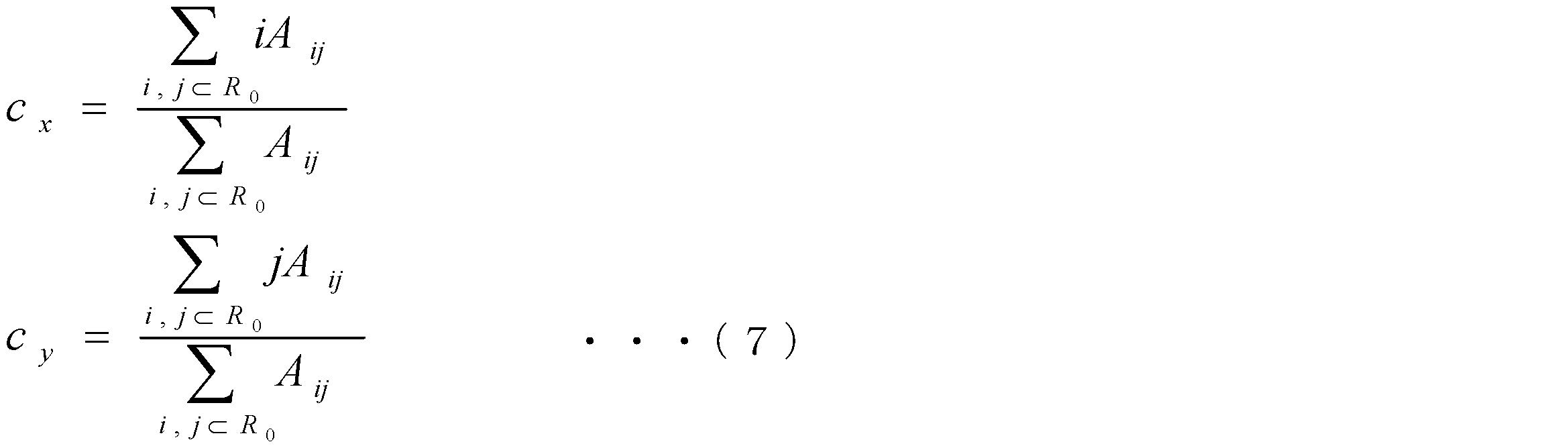
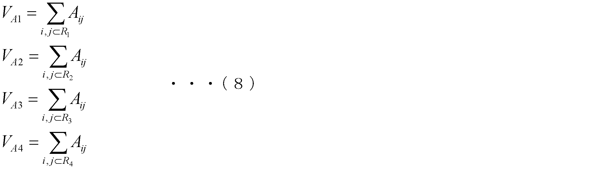
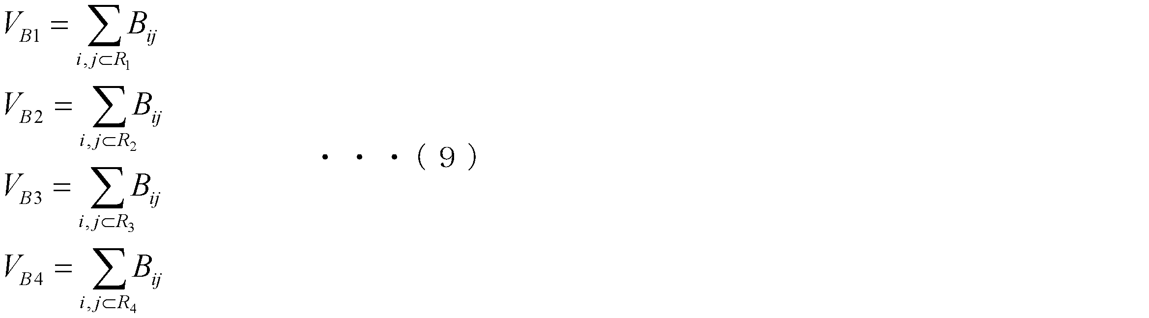


上述した実施形態では、位相パターンPAを表示した状態で光強度分布データDAを取得し(ステップS13)、位相パターンPBを表示した状態で光強度分布データDBを取得したのち(ステップS15)、これらの光強度分布データDA,DBから算出される特徴量VA1~VA4と特徴量VB1~VB4との差分ΔV1~ΔV4を求めている。しかしながら、特徴量VA1~VA4のみに基づいてキャリブレーションを行うことも可能である。

上記実施形態および第1変形例では、特徴量の算出の際、領域L0に隣接する領域L1~L4について特徴量VA1~VA4及び特徴量VB1~VB4を算出し、これらの特徴量に基づいてキャリブレーションを行う。しかしながら、領域L0についての特徴量に基づいてキャリブレーションを行ってもよい。


上記実施形態および各変形例では、図20に示されたステップS18において変調面11aと波面センサ12との対応関係を調整する際、位相パターンPAの第1の領域B1を行方向(又は列方向)に一画素だけ移動させている。しかしながら、ステップS18における第1の領域B1の移動量は一画素に限られない。例えば、値Vx及びVyの大きさに応じて、第1の領域B1の移動量を変化させてもよい。一例としては、値Vxが所定値よりも小さいときには一回当たりの第1の領域B1の移動量を一画素とし、値Vxが所定値よりも大きいときには、一回当たりの第1の領域B1の移動量を2画素や3画素などとすることができる。なお、前述した第2変形例にこの方法を適用する場合、差分ΔV0の大きさに応じて、第1の領域B1の移動量を決定することができる。
上記実施形態および各変形例では、波面部分A4(図7を参照)の大きさが一つのレンズ124の径と一致するように、第1の領域B1の大きさを設定している(数式(5)を参照)。しかしながら、第1の領域B1の大きさはこれに限られず、以下に示すような種々の大きさに設定されてもよい。

上記実施形態および各変形例では、図20に示されたステップS12において、少なくとも一方向に線形性を有する第1の位相パターンを第1の領域B1に表示し、空間的に非線形な第2の位相パターンを第2の領域B2に表示している。しかしながら、少なくとも一方向に線形性を有する位相パターンを第2の領域B2に表示し、空間的に非線形な位相パターンを第1の領域B1に表示した場合であっても、上記実施形態と同様の効果を得ることができる。なお、この場合、前述した数式(2)は、次のように書き換えられる。


上記実施形態および各変形例では、変調面11aにおいて第1の領域B1が一つのみ設定された場合を説明しているが、第1の領域B1は複数箇所設定されてもよい。これにより、複数の第1の領域B1のそれぞれに関して算出された特徴量に基づいて各第1の領域B1と波面センサ12との位置ずれを調べたのち、これらの位置ずれを統計的に処理し、その結果に基づいて、変調面11aと波面センサ12との対応関係をより精度良く調整することができる。
上記実施形態および各変形例では、第1の領域B1(第5変形例では第2の領域B2)に表示される少なくとも一方向に線形性を有する第1の位相パターンの例として、定数a(若しくはa’)で表される略均一な分布を例示した。しかしながら、第1の位相パターンは、少なくとも一方向に傾斜した(線形的に変化する)位相分布であってもよい。このような位相パターンを含むキャリブレーション用の特殊な位相パターンPAは、次の数式(18)により表される。

第1の領域B1(第5変形例では第2の領域B2)に表示される第1の位相パターンは、図30に示されるような、第1の方向(例えば行方向)における位相分布がシリンドリカルレンズ効果を有し、第2の方向(例えば列方向)において位相値が略均一であるような位相分布であってもよい。このような位相分布を含むキャリブレーション用の特殊な位相パターンPAは、次の数式(19)により表される。


第1の領域B1(第5変形例では第2の領域B2)に表示される第1の位相パターンは、図31に示されるような、第1の方向(例えば行方向)における位相分布が回折格子を構成し、第2の方向(例えば列方向)において位相値が略均一であるような位相分布であってもよい。図31に示される第1の位相パターンを含む位相パターンPAが変調面11aに表示されると、波面センサ12では、行方向に分離される複数の集光スポットPが形成される。従って、この位相パターンPAを用いて、列方向のキャリブレーションを行うことができる。なお、行方向のキャリブレーションを行う際には、上記第1の方向を列方向とし、上記第2の方向を行方向とした第1の位相パターンを含む位相パターンPAを、変調面11aに表示することができる。
第1の領域B1(第5変形例では第2の領域B2)に表示される第1の位相パターンは、上記実施形態および第7~9変形例に示された位相分布を互いに重ね合わせた合成パターンを含んでもよい。図32は、そのような重ね合わせによって得られる合成パターンの例を示す図である。図32(a)に示される位相パターンは図30に示されたものであり、図32(b)に示される位相パターンは、図28に示された位相パターンを90°回転させたものである。そして、図32(c)に示される位相パターンは、これらを重ね合わせた合成パターンである。図32(c)に示される位相パターンは第1の方向における位相分布が2次関数を有し、第2の方向における位相分布が線形関数を有する位相分布の位相パターンである。図32(c)に示された合成パターンを含む位相パターンPAが変調面11aに表示されると、波面センサ12では、行方向に拡散し、列方向に集束された集光スポットPが形成される。従って、この位相パターンPAを用いて、列方向のキャリブレーションを行うことができる。なお、行方向のキャリブレーションを行う際には、第1の方向を列方向とし、第2の方向を行方向とした上記合成パターンを第1の位相パターンとして含む位相パターンPAを、変調面11aに表示することができる。
上記実施形態および各変形例では、第2の領域B2(第5変形例では第1の領域B1)に表示される空間的に非線形な第2の位相パターンの例として、ランダム分布(図12)及びデフォーカス分布(図13)を例示した。第2の位相パターンはこれらに限られず、明瞭な集光スポットPが形成されないような位相分布を有していればよい。このような位相分布としては、例えばFresnel Zone Plate(FZP)型の位相パターンが挙げられる。FZP型位相パターンは、入射された略均一な位相値を有する光像Laを集光或いは発散させる作用を有する。従って、FZP型位相パターンにより集光或いは発散された光像Laがレンズ124に入射すると、集光スポットPの光軸方向の位置が、レンズ124の焦点面(すなわちイメージセンサ122の表面)からずれる。このため、イメージセンサ122の表面では、ぼけた点像が形成される。

上記実施形態および各変形例では、波面センサ12のレンズアレイ120として、図3に示されたように、複数のレンズ124が二次元格子状に配列された形態を例示している。しかしながら、波面センサ12のレンズアレイはこのような形態に限られない。例えば、図33に示されるように、レンズアレイ120は、正六角形の複数のレンズ128が隙間無く並んだハニカム構造を有していてもよい。なお、この場合、第1の領域B1は六角形に設定されてもよい。また、図21に示された領域L0等や特徴量計算領域R0等は、図34に示されるように、全て六角形に設定されてもよい。更に、図20のステップS18において算出された値Vx及びVyに相当する値は、領域L0を挟んで対向する領域(具体的には、領域L1及びL2、領域L3及びL4、並びに領域L5及びL6)において算出される特徴量から求められる。
上記実施形態および各変形例では、第1の領域B1に対応する波面部分A4(図10を参照)の大きさが、レンズ124の径のn1倍(但し、n1は自然数)であるとしている。しかしながら、n1は自然数ではない実数(例えば0.8や1.2など)であってもよい。ここで、n1がそのような値をとる場合における、第1の領域B1の大きさとキャリブレーション精度との関係について説明する。図35は、図7の波面センサ12付近を拡大して示す図である。図35(a)は、第1の領域B1に対応する波面部分A4の幅が一つのレンズ124の径よりも若干大きい場合を示しており、図35(b)は、波面部分A4の幅が一つのレンズ124の径よりも若干小さい場合を示している。
上記実施形態では、図20に示されたステップS18において位相パターンPAの第1の領域B1を一画素ずつ移動させながら、ステップS12~S18を繰り返し行っているが、次のような形態も可能である。すなわち、キャリブレーションを行う前に、ステップS12~S18を行うことにより、複数の(例えば、第1の領域B1を構成する画素数と同じ数の)値Vx及びVyの組を予め取得しておく。そして、キャリブレーション時には、ステップS12~S18(値Vx及びVyの算出まで)を一回のみ行い、得られた値Vx及びVyと、予め取得しておいた複数の値Vx及びVyの組とを比較する。このとき、例えば得られた値Vx及びVyと予め取得しておいた複数の値Vx及びVyの組との類似性の度合い(相関係数)を算出してもよい。そして、得られた値Vx及びVyに最も近い値Vx及びVyの組が算出された際の第1の領域B1の位置に基づいて、変調面11aと波面センサ12との対応関係を調整する。これにより、図20に示されたステップS12~S18を繰り返すことなく、キャリブレーションを短時間で行うことができる。なお、値Vx及びVyの組に代えて、予め取得しておいた複数の光強度分布データDAや特徴量を比較対象としてもよい。
上記実施形態および各変形例において、第1の領域B1と、該第1の領域B1に対応するレンズ124とのずれ幅の最大値は、第1の領域B1の一辺の画素数wの±1/2倍である。従って、第1の領域B1と、該第1の領域B1に対応するレンズ124との位置関係の組み合わせの数はw×w通りである。そして、そのw×w通りの位置関係のうち、第1の領域B1の位置とレンズ124の位置とが完全に一致するのは一通りだけであり、他の(w×w-1)通りの場合、第1の領域B1は、レンズ124に対して行方向若しくは列方向、又はその双方に、各位置関係毎に固有のずれ量を有している。

Claims (9)
- 変調面に入射した光像の位相を空間的に変調する空間光変調器と、複数のレンズが二次元状に配列されたレンズアレイ、並びに前記レンズアレイによって形成された集光スポットを含む光強度分布を検出する光検出素子を有しており前記空間光変調器から変調後の前記光像を受ける波面センサとを備え、前記光強度分布から得られる前記光像の波面形状に基づいて前記空間光変調器に表示される位相パターンを制御することにより波面歪みを補償する補償光学システムにおいて、前記変調面と前記波面センサとの対応関係を調整する方法であって、
前記複数のレンズのうちの一若しくは互いに隣接する二以上のレンズに対応させようとする前記変調面上の第1の領域に、少なくとも一方向に線形性を有する第1の位相パターン及び空間的に非線形な第2の位相パターンのうち一方を表示させ、前記第1の領域を囲む第2の領域に前記第1及び第2の位相パターンのうち他方を表示させた状態で、前記光検出素子により前記光強度分布を取得する第1の光強度分布取得ステップと、
前記第1の光強度分布取得ステップにおいて得られた前記光強度分布に含まれる前記集光スポットの明瞭さに基づいて、前記変調面と前記波面センサとの対応関係を調整する調整ステップと、
を備える補償光学システムの調整方法。 - 空間的に非線形な位相パターンを前記第1及び第2の領域に表示させた状態で、前記光検出素子により前記光強度分布を取得する第2の光強度分布取得ステップと、
前記第1の光強度分布取得ステップにおいて得られた前記光強度分布に含まれる前記集光スポットの明瞭さに関する数値と、前記第2の光強度分布取得ステップにおいて得られた前記光強度分布に含まれる前記集光スポットの明瞭さに関する数値との差分を算出する差分算出ステップと、
を更に備え、
前記調整ステップの際に、前記第1の光強度分布取得ステップにおいて得られた前記光強度分布に含まれる前記集光スポットの明瞭さに代えて、前記差分算出ステップにおいて得られた前記差分に基づいて前記変調面と前記波面センサとの対応関係を調整する請求項1に記載の補償光学システムの調整方法。 - 前記調整ステップにおける前記変調面と前記波面センサとの対応関係の調整とは、波面歪み補償用の前記位相パターンを表示する際に前記変調面上に想定される位置座標と前記波面センサとの相対位置関係の調整である請求項1または2に記載の補償光学システムの調整方法。
- 前記調整ステップにおける前記変調面と前記波面センサとの対応関係の調整とは、前記波面センサの取り付け位置と、前記空間光変調器の取り付け位置との相対関係の調整である請求項1または2に記載の補償光学システムの調整方法。
- 前記複数のレンズの配列方向における前記第1の領域の幅が、前記複数のレンズの配列ピッチの(n1/M)倍(但し、n1は自然数であり、Mは前記変調面と前記レンズアレイとの間の光学系の結像倍率)である請求項1~4のいずれか一項に記載の補償光学システムの調整方法。
- 前記空間的に非線形な位相パターンが、位相の大きさの分布が不規則であるランダム分布、および前記集光スポットを拡径するデフォーカス分布のうち少なくとも一つを含む請求項1~5のいずれか一項に記載の補償光学システムの調整方法。
- 前記少なくとも一方向に線形性を有する位相パターンが、略均一な位相分布、少なくとも一方向に傾斜した位相分布、第1の方向においてシリンドリカルレンズ効果を有し、該第1の方向と交差する第2の方向において略均一である位相分布、及び、第1の方向において回折格子を構成し、該第1の方向と交差する第2の方向において略均一である位相分布のうち少なくとも一つを含む請求項1~6のいずれか一項に記載の補償光学システムの調整方法。
- 変調面に入射した光像の位相を空間的に変調する空間光変調器と、
複数のレンズが二次元状に配列されたレンズアレイ、並びに前記レンズアレイによって形成された集光スポットを含む光強度分布を検出する光検出素子を有しており前記空間光変調器から変調後の前記光像を受ける波面センサと、
前記光強度分布から得られる前記光像の波面形状に基づいて前記空間光変調器に表示される位相パターンを制御することにより波面歪みを補償する制御部と、
を備え、
前記制御部が、前記複数のレンズのうちの一若しくは互いに隣接する二以上のレンズに対応させようとする前記変調面上の第1の領域に、少なくとも一方向に線形性を有する第1の位相パターン及び空間的に非線形な第2の位相パターンのうち一方を表示させ、前記第1の領域を囲む第2の領域に前記第1及び第2の位相パターンのうち他方を表示させた状態で、前記光検出素子により前記光強度分布を取得し、該光強度分布に含まれる前記集光スポットの明瞭さに基づいて前記変調面と前記波面センサとの対応関係を調整する補償光学システム。 - 変調面に入射した光像の位相を空間的に変調する空間光変調器と、複数のレンズが二次元状に配列されたレンズアレイ、並びに前記レンズアレイによって形成された集光スポットを含む光強度分布を検出する光検出素子を有しており前記空間光変調器から変調後の前記光像を受ける波面センサと、前記光強度分布から得られる前記光像の波面形状に基づいて前記空間光変調器に表示される位相パターンを制御することにより波面歪みを補償する制御部とを備える補償光学システムにおいて、前記制御部の動作を制御するための補償光学システム用プログラムを記憶する記録媒体であって、
前記補償光学システム用プログラムは、
前記複数のレンズのうちの一若しくは互いに隣接する二以上のレンズに対応させようとする前記変調面上の第1の領域に、少なくとも一方向に線形性を有する第1の位相パターン及び空間的に非線形な第2の位相パターンのうち一方を表示させ、前記第1の領域を囲む第2の領域に前記第1及び第2の位相パターンのうち他方を表示させた状態で、前記光検出素子により前記光強度分布を取得する第1の光強度分布取得ステップと、
前記第1の光強度分布取得ステップにおいて得られた前記光強度分布に含まれる前記集光スポットの明瞭さに基づいて、前記変調面と前記波面センサとの対応関係を調整する調整ステップと、
を前記制御部に実行させる、
補償光学システム用プログラムを記憶する記録媒体。
Priority Applications (5)
| Application Number | Priority Date | Filing Date | Title |
|---|---|---|---|
| KR1020157037214A KR102128642B1 (ko) | 2013-06-06 | 2014-05-29 | 보상 광학 시스템의 조정 방법, 보상 광학 시스템, 및 보상 광학 시스템용 프로그램을 기억하는 기록 매체 |
| US14/895,588 US9594245B2 (en) | 2013-06-06 | 2014-05-29 | Adjustment method for adaptive optics system, adaptive optics system, and storage medium storing program for adaptive optics system |
| JP2015521417A JP6259825B2 (ja) | 2013-06-06 | 2014-05-29 | 補償光学システムの調整方法、補償光学システム、及び補償光学システム用プログラムを記憶する記録媒体 |
| CN201480031849.3A CN105264428B (zh) | 2013-06-06 | 2014-05-29 | 自适应光学系统的调整方法、自适应光学系统和存储自适应光学系统用程序的记录介质 |
| DE112014002683.2T DE112014002683B4 (de) | 2013-06-06 | 2014-05-29 | Justierverfahren für adaptives Optiksystem, adaptives Optiksystem und Speichermedium, das ein Programm für ein adaptives Optiksystem speichert |
Applications Claiming Priority (2)
| Application Number | Priority Date | Filing Date | Title |
|---|---|---|---|
| JP2013-119852 | 2013-06-06 | ||
| JP2013119852 | 2013-06-06 |
Publications (1)
| Publication Number | Publication Date |
|---|---|
| WO2014196448A1 true WO2014196448A1 (ja) | 2014-12-11 |
Family
ID=52008094
Family Applications (1)
| Application Number | Title | Priority Date | Filing Date |
|---|---|---|---|
| PCT/JP2014/064294 Ceased WO2014196448A1 (ja) | 2013-06-06 | 2014-05-29 | 補償光学システムの調整方法、補償光学システム、及び補償光学システム用プログラムを記憶する記録媒体 |
Country Status (6)
| Country | Link |
|---|---|
| US (1) | US9594245B2 (ja) |
| JP (1) | JP6259825B2 (ja) |
| KR (1) | KR102128642B1 (ja) |
| CN (1) | CN105264428B (ja) |
| DE (1) | DE112014002683B4 (ja) |
| WO (1) | WO2014196448A1 (ja) |
Cited By (3)
| Publication number | Priority date | Publication date | Assignee | Title |
|---|---|---|---|---|
| WO2018185740A1 (en) * | 2017-04-06 | 2018-10-11 | Yoav Berlatzky | Wavefront sensor and method of using it |
| JP2019176214A (ja) * | 2018-03-27 | 2019-10-10 | 株式会社日立製作所 | 撮像装置、撮像モジュールおよび撮像方法 |
| CN112639421A (zh) * | 2018-09-07 | 2021-04-09 | 伯格利-格拉维瑞斯股份有限公司 | 自适应激光束整形 |
Families Citing this family (22)
| Publication number | Priority date | Publication date | Assignee | Title |
|---|---|---|---|---|
| JP6298050B2 (ja) * | 2013-06-06 | 2018-03-20 | 浜松ホトニクス株式会社 | 補償光学システムの対応関係特定方法、波面歪み補償方法、補償光学システム、および補償光学システム用プログラムを記憶する記録媒体 |
| EP2908341B1 (en) * | 2014-02-18 | 2018-07-11 | ams AG | Semiconductor device with surface integrated focusing element |
| JP6768444B2 (ja) * | 2016-10-14 | 2020-10-14 | 浜松ホトニクス株式会社 | レーザ加工装置、及び、動作確認方法 |
| US20180301484A1 (en) * | 2017-04-17 | 2018-10-18 | Semiconductor Components Industries, Llc | Image sensors with high dynamic range and autofocusing hexagonal pixels |
| JP6969164B2 (ja) * | 2017-05-31 | 2021-11-24 | 株式会社リコー | 評価装置、評価プログラム及び評価方法 |
| KR20190054353A (ko) | 2017-11-13 | 2019-05-22 | 한국 천문 연구원 | 범용 적응 광학 시스템 |
| CN110501826B (zh) * | 2018-05-18 | 2021-09-07 | 中国科学院上海光学精密机械研究所 | 基于相位载波的提高光束质量的方法 |
| CN109358030B (zh) * | 2018-11-26 | 2020-10-30 | 浙江大学 | 一种具有自动对准功能的多色超分辨显微镜系统 |
| CN109520712B (zh) * | 2018-12-03 | 2021-08-17 | 江苏慧光电子科技有限公司 | 光学检测方法、系统及光学器件制造系统 |
| CN109683312B (zh) * | 2019-01-22 | 2021-03-12 | 中国工程物理研究院激光聚变研究中心 | 一种自适应光学系统像传递关系的调节方法 |
| FR3092396B1 (fr) * | 2019-01-31 | 2021-04-09 | Centre Nat Rech Scient | Système de contrôle de surfaces d’onde optique par filtre à gradient de densité |
| CN111609995B (zh) * | 2019-02-26 | 2025-07-22 | 弗提图德萨沃有限公司 | 一种光学模组装调测试方法及装置 |
| US11662597B2 (en) * | 2019-07-03 | 2023-05-30 | Texas Instruments Incorporated | Homogenizing lens array for display imaging |
| CN112161584A (zh) * | 2020-10-27 | 2021-01-01 | 龚海 | 一种基于照明光倾斜调制的波前三维显微镜 |
| CN113295286A (zh) * | 2021-05-20 | 2021-08-24 | 中国科学院西安光学精密机械研究所 | 一种夏克-哈特曼波前传感器测量系统及相位恢复方法 |
| CN113534255B (zh) | 2021-07-07 | 2024-07-16 | 南方海洋科学与工程广东省实验室(湛江) | 一种任意形态不连续面自适应表达的方法 |
| CN113267909B (zh) * | 2021-07-19 | 2021-10-08 | 军事科学院系统工程研究院网络信息研究所 | 基于波前畸变补偿的防窥显示方法 |
| JPWO2023210115A1 (ja) * | 2022-04-28 | 2023-11-02 | ||
| WO2024030902A1 (en) * | 2022-08-01 | 2024-02-08 | California Institute Of Technology | Complex-wavefront photonic transceiver processor |
| CN115685565B (zh) * | 2022-08-05 | 2024-07-26 | 华侨大学 | 一种透过散射介质的复杂光场的调控方法及装置 |
| KR102841979B1 (ko) * | 2022-09-15 | 2025-08-04 | 서울대학교산학협력단 | 이미지 분할 기반 광검출 시스템 및 방법 |
| CN119803273B (zh) * | 2025-03-13 | 2025-07-11 | 中国科学院长春光学精密机械与物理研究所 | 复杂曲面光学元件的补偿装置设计方法及补偿检测装置 |
Citations (4)
| Publication number | Priority date | Publication date | Assignee | Title |
|---|---|---|---|---|
| JPH0915057A (ja) * | 1995-06-26 | 1997-01-17 | Mitsubishi Electric Corp | 波面センサ並びに波面計測方法 |
| JP2009162614A (ja) * | 2008-01-07 | 2009-07-23 | Mitsubishi Electric Corp | 光波面計測装置 |
| JP2010261810A (ja) * | 2009-05-07 | 2010-11-18 | Mitsubishi Electric Corp | 波面センサ |
| JP2013250525A (ja) * | 2012-06-04 | 2013-12-12 | Hamamatsu Photonics Kk | 補償光学システムの調整方法および補償光学システム |
Family Cites Families (15)
| Publication number | Priority date | Publication date | Assignee | Title |
|---|---|---|---|---|
| US6771417B1 (en) * | 1997-08-01 | 2004-08-03 | Carl Zeiss Jena Gmbh | Applications of adaptive optics in microscopy |
| US6827442B2 (en) | 2001-09-12 | 2004-12-07 | Denwood F. Ross | Ophthalmic wavefront measuring devices |
| GB0314444D0 (en) * | 2003-06-20 | 2003-07-23 | Univ Heriot Watt | Novel wavefront sensor |
| US7333215B2 (en) * | 2003-06-25 | 2008-02-19 | The Boeing Company | Adaptive optics control system |
| JP4531431B2 (ja) * | 2004-04-02 | 2010-08-25 | 浜松ホトニクス株式会社 | 波面補償装置、波面補償方法、プログラム、及び、記録媒体 |
| WO2006035775A1 (ja) * | 2004-09-27 | 2006-04-06 | Hamamatsu Photonics K.K. | 空間光変調装置、光学処理装置、カップリングプリズム、及び、カップリングプリズムの使用方法 |
| US7649160B2 (en) * | 2005-02-23 | 2010-01-19 | Lyncee Tec S.A. | Wave front sensing method and apparatus |
| WO2007070006A1 (en) * | 2005-12-13 | 2007-06-21 | Agency For Science, Technology And Research | Optical wavefront sensor |
| US8451427B2 (en) * | 2007-09-14 | 2013-05-28 | Nikon Corporation | Illumination optical system, exposure apparatus, optical element and manufacturing method thereof, and device manufacturing method |
| JP5139832B2 (ja) | 2008-02-14 | 2013-02-06 | 浜松ホトニクス株式会社 | 観察装置 |
| JP5692969B2 (ja) * | 2008-09-01 | 2015-04-01 | 浜松ホトニクス株式会社 | 収差補正方法、この収差補正方法を用いたレーザ加工方法、この収差補正方法を用いたレーザ照射方法、収差補正装置、及び、収差補正プログラム |
| US8551730B2 (en) * | 2008-10-24 | 2013-10-08 | The Regents Of The University Of California | Use of a reference source with adaptive optics in biological microscopy |
| JP5599563B2 (ja) * | 2008-12-25 | 2014-10-01 | 浜松ホトニクス株式会社 | 光制御装置および光制御方法 |
| JP2012037572A (ja) * | 2010-08-03 | 2012-02-23 | Hamamatsu Photonics Kk | レーザ光整形及び波面制御用光学系 |
| US8237835B1 (en) * | 2011-05-19 | 2012-08-07 | Aeon Imaging, LLC | Confocal imaging device using spatially modulated illumination with electronic rolling shutter detection |
-
2014
- 2014-05-29 US US14/895,588 patent/US9594245B2/en active Active
- 2014-05-29 JP JP2015521417A patent/JP6259825B2/ja active Active
- 2014-05-29 DE DE112014002683.2T patent/DE112014002683B4/de active Active
- 2014-05-29 KR KR1020157037214A patent/KR102128642B1/ko not_active Expired - Fee Related
- 2014-05-29 CN CN201480031849.3A patent/CN105264428B/zh active Active
- 2014-05-29 WO PCT/JP2014/064294 patent/WO2014196448A1/ja not_active Ceased
Patent Citations (4)
| Publication number | Priority date | Publication date | Assignee | Title |
|---|---|---|---|---|
| JPH0915057A (ja) * | 1995-06-26 | 1997-01-17 | Mitsubishi Electric Corp | 波面センサ並びに波面計測方法 |
| JP2009162614A (ja) * | 2008-01-07 | 2009-07-23 | Mitsubishi Electric Corp | 光波面計測装置 |
| JP2010261810A (ja) * | 2009-05-07 | 2010-11-18 | Mitsubishi Electric Corp | 波面センサ |
| JP2013250525A (ja) * | 2012-06-04 | 2013-12-12 | Hamamatsu Photonics Kk | 補償光学システムの調整方法および補償光学システム |
Non-Patent Citations (3)
| Title |
|---|
| ABDUL AWWAL ET AL.: "Characterization and Operation of a Liquid Crystal Adaptive Optics Phoropter", PROC. OF SPIE, vol. 5169, 31 December 2003 (2003-12-31), pages 104 - 122 * |
| HONGXIN HUANG ET AL.: "Adaptive aberration compensation sysytem using a high-resolution liquid crystal on silicon spatial phase modulator", PROC. OF SPIE, vol. 7156, 3 December 2008 (2008-12-03), pages 71560F - 1-71560F-10 * |
| JASON PORTER ET AL., ADAPTIVE OPTICS FOR VISION SCIENCE, June 2006 (2006-06-01), pages 477 - 509 * |
Cited By (6)
| Publication number | Priority date | Publication date | Assignee | Title |
|---|---|---|---|---|
| WO2018185740A1 (en) * | 2017-04-06 | 2018-10-11 | Yoav Berlatzky | Wavefront sensor and method of using it |
| KR20190137104A (ko) * | 2017-04-06 | 2019-12-10 | 피엑스이 컴퓨테이셔널 이미징 엘티디 | 파두 센서 및 이를 사용하는 방법 |
| US11293806B2 (en) | 2017-04-06 | 2022-04-05 | Pxe Computational Imagimg Ltd | Wavefront sensor and method of using it |
| KR102537284B1 (ko) * | 2017-04-06 | 2023-05-26 | 피엑스이 컴퓨테이셔널 이미징 엘티디 | 파두 센서 및 이를 사용하는 방법 |
| JP2019176214A (ja) * | 2018-03-27 | 2019-10-10 | 株式会社日立製作所 | 撮像装置、撮像モジュールおよび撮像方法 |
| CN112639421A (zh) * | 2018-09-07 | 2021-04-09 | 伯格利-格拉维瑞斯股份有限公司 | 自适应激光束整形 |
Also Published As
| Publication number | Publication date |
|---|---|
| JP6259825B2 (ja) | 2018-01-10 |
| US9594245B2 (en) | 2017-03-14 |
| US20160131901A1 (en) | 2016-05-12 |
| CN105264428A (zh) | 2016-01-20 |
| DE112014002683B4 (de) | 2024-04-18 |
| CN105264428B (zh) | 2018-06-29 |
| DE112014002683T5 (de) | 2016-03-10 |
| JPWO2014196448A1 (ja) | 2017-02-23 |
| KR102128642B1 (ko) | 2020-06-30 |
| KR20160016962A (ko) | 2016-02-15 |
Similar Documents
| Publication | Publication Date | Title |
|---|---|---|
| JP6259825B2 (ja) | 補償光学システムの調整方法、補償光学システム、及び補償光学システム用プログラムを記憶する記録媒体 | |
| JP6226977B2 (ja) | 補償光学システムの角度ずれ検出方法、補償光学システムの結像倍率検出方法、及び補償光学システム | |
| CN105264429B (zh) | 自适应光学系统的对应关系确定方法、波前畸变补偿方法、自适应光学系统及存储自适应光学系统用程序的记录介质 | |
| CN105263396B (zh) | 自适应光学系统的对应关系确定方法、自适应光学系统和存储自适应光学系统用程序的记录介质 | |
| JP5919100B2 (ja) | 補償光学システムの調整方法および補償光学システム | |
| US8748801B2 (en) | Discrete wavefront sampling using a variable transmission filter | |
| JP5139832B2 (ja) | 観察装置 | |
| US9727024B2 (en) | Phase modulation method and phase modulating device |
Legal Events
| Date | Code | Title | Description |
|---|---|---|---|
| WWE | Wipo information: entry into national phase |
Ref document number: 201480031849.3 Country of ref document: CN |
|
| 121 | Ep: the epo has been informed by wipo that ep was designated in this application |
Ref document number: 14807349 Country of ref document: EP Kind code of ref document: A1 |
|
| ENP | Entry into the national phase |
Ref document number: 2015521417 Country of ref document: JP Kind code of ref document: A |
|
| WWE | Wipo information: entry into national phase |
Ref document number: 14895588 Country of ref document: US |
|
| WWE | Wipo information: entry into national phase |
Ref document number: 112014002683 Country of ref document: DE |
|
| ENP | Entry into the national phase |
Ref document number: 20157037214 Country of ref document: KR Kind code of ref document: A |
|
| 122 | Ep: pct application non-entry in european phase |
Ref document number: 14807349 Country of ref document: EP Kind code of ref document: A1 |