WO2014192333A1 - 発光装置 - Google Patents
発光装置 Download PDFInfo
- Publication number
- WO2014192333A1 WO2014192333A1 PCT/JP2014/053727 JP2014053727W WO2014192333A1 WO 2014192333 A1 WO2014192333 A1 WO 2014192333A1 JP 2014053727 W JP2014053727 W JP 2014053727W WO 2014192333 A1 WO2014192333 A1 WO 2014192333A1
- Authority
- WO
- WIPO (PCT)
- Prior art keywords
- light
- emitting device
- nanoparticles
- light emitting
- translucent member
- Prior art date
- Legal status (The legal status is an assumption and is not a legal conclusion. Google has not performed a legal analysis and makes no representation as to the accuracy of the status listed.)
- Ceased
Links
Images

Classifications
-
- F—MECHANICAL ENGINEERING; LIGHTING; HEATING; WEAPONS; BLASTING
- F21—LIGHTING
- F21V—FUNCTIONAL FEATURES OR DETAILS OF LIGHTING DEVICES OR SYSTEMS THEREOF; STRUCTURAL COMBINATIONS OF LIGHTING DEVICES WITH OTHER ARTICLES, NOT OTHERWISE PROVIDED FOR
- F21V9/00—Elements for modifying spectral properties, polarisation or intensity of the light emitted, e.g. filters
- F21V9/30—Elements containing photoluminescent material distinct from or spaced from the light source
-
- F—MECHANICAL ENGINEERING; LIGHTING; HEATING; WEAPONS; BLASTING
- F21—LIGHTING
- F21K—NON-ELECTRIC LIGHT SOURCES USING LUMINESCENCE; LIGHT SOURCES USING ELECTROCHEMILUMINESCENCE; LIGHT SOURCES USING CHARGES OF COMBUSTIBLE MATERIAL; LIGHT SOURCES USING SEMICONDUCTOR DEVICES AS LIGHT-GENERATING ELEMENTS; LIGHT SOURCES NOT OTHERWISE PROVIDED FOR
- F21K9/00—Light sources using semiconductor devices as light-generating elements, e.g. using light-emitting diodes [LED] or lasers
- F21K9/60—Optical arrangements integrated in the light source, e.g. for improving the colour rendering index or the light extraction
- F21K9/64—Optical arrangements integrated in the light source, e.g. for improving the colour rendering index or the light extraction using wavelength conversion means distinct or spaced from the light-generating element, e.g. a remote phosphor layer
-
- F—MECHANICAL ENGINEERING; LIGHTING; HEATING; WEAPONS; BLASTING
- F21—LIGHTING
- F21V—FUNCTIONAL FEATURES OR DETAILS OF LIGHTING DEVICES OR SYSTEMS THEREOF; STRUCTURAL COMBINATIONS OF LIGHTING DEVICES WITH OTHER ARTICLES, NOT OTHERWISE PROVIDED FOR
- F21V3/00—Globes; Bowls; Cover glasses
- F21V3/04—Globes; Bowls; Cover glasses characterised by materials, surface treatments or coatings
-
- F—MECHANICAL ENGINEERING; LIGHTING; HEATING; WEAPONS; BLASTING
- F21—LIGHTING
- F21V—FUNCTIONAL FEATURES OR DETAILS OF LIGHTING DEVICES OR SYSTEMS THEREOF; STRUCTURAL COMBINATIONS OF LIGHTING DEVICES WITH OTHER ARTICLES, NOT OTHERWISE PROVIDED FOR
- F21V9/00—Elements for modifying spectral properties, polarisation or intensity of the light emitted, e.g. filters
- F21V9/06—Elements for modifying spectral properties, polarisation or intensity of the light emitted, e.g. filters for filtering out ultraviolet radiation
-
- G—PHYSICS
- G02—OPTICS
- G02B—OPTICAL ELEMENTS, SYSTEMS OR APPARATUS
- G02B1/00—Optical elements characterised by the material of which they are made; Optical coatings for optical elements
- G02B1/10—Optical coatings produced by application to, or surface treatment of, optical elements
- G02B1/11—Anti-reflection coatings
- G02B1/113—Anti-reflection coatings using inorganic layer materials only
- G02B1/115—Multilayers
-
- G—PHYSICS
- G02—OPTICS
- G02B—OPTICAL ELEMENTS, SYSTEMS OR APPARATUS
- G02B1/00—Optical elements characterised by the material of which they are made; Optical coatings for optical elements
- G02B1/10—Optical coatings produced by application to, or surface treatment of, optical elements
- G02B1/11—Anti-reflection coatings
- G02B1/118—Anti-reflection coatings having sub-optical wavelength surface structures designed to provide an enhanced transmittance, e.g. moth-eye structures
-
- G—PHYSICS
- G02—OPTICS
- G02B—OPTICAL ELEMENTS, SYSTEMS OR APPARATUS
- G02B5/00—Optical elements other than lenses
- G02B5/02—Diffusing elements; Afocal elements
- G02B5/0205—Diffusing elements; Afocal elements characterised by the diffusing properties
- G02B5/0236—Diffusing elements; Afocal elements characterised by the diffusing properties the diffusion taking place within the volume of the element
- G02B5/0242—Diffusing elements; Afocal elements characterised by the diffusing properties the diffusion taking place within the volume of the element by means of dispersed particles
-
- H—ELECTRICITY
- H05—ELECTRIC TECHNIQUES NOT OTHERWISE PROVIDED FOR
- H05B—ELECTRIC HEATING; ELECTRIC LIGHT SOURCES NOT OTHERWISE PROVIDED FOR; CIRCUIT ARRANGEMENTS FOR ELECTRIC LIGHT SOURCES, IN GENERAL
- H05B33/00—Electroluminescent light sources
- H05B33/12—Light sources with substantially two-dimensional [2D] radiating surfaces
- H05B33/14—Light sources with substantially two-dimensional [2D] radiating surfaces characterised by the chemical or physical composition or the arrangement of the electroluminescent material, or by the simultaneous addition of the electroluminescent material in or onto the light source
-
- B—PERFORMING OPERATIONS; TRANSPORTING
- B82—NANOTECHNOLOGY
- B82Y—SPECIFIC USES OR APPLICATIONS OF NANOSTRUCTURES; MEASUREMENT OR ANALYSIS OF NANOSTRUCTURES; MANUFACTURE OR TREATMENT OF NANOSTRUCTURES
- B82Y20/00—Nanooptics, e.g. quantum optics or photonic crystals
-
- F—MECHANICAL ENGINEERING; LIGHTING; HEATING; WEAPONS; BLASTING
- F21—LIGHTING
- F21Y—INDEXING SCHEME ASSOCIATED WITH SUBCLASSES F21K, F21L, F21S and F21V, RELATING TO THE FORM OR THE KIND OF THE LIGHT SOURCES OR OF THE COLOUR OF THE LIGHT EMITTED
- F21Y2115/00—Light-generating elements of semiconductor light sources
- F21Y2115/10—Light-emitting diodes [LED]
-
- Y—GENERAL TAGGING OF NEW TECHNOLOGICAL DEVELOPMENTS; GENERAL TAGGING OF CROSS-SECTIONAL TECHNOLOGIES SPANNING OVER SEVERAL SECTIONS OF THE IPC; TECHNICAL SUBJECTS COVERED BY FORMER USPC CROSS-REFERENCE ART COLLECTIONS [XRACs] AND DIGESTS
- Y10—TECHNICAL SUBJECTS COVERED BY FORMER USPC
- Y10S—TECHNICAL SUBJECTS COVERED BY FORMER USPC CROSS-REFERENCE ART COLLECTIONS [XRACs] AND DIGESTS
- Y10S977/00—Nanotechnology
- Y10S977/70—Nanostructure
- Y10S977/773—Nanoparticle, i.e. structure having three dimensions of 100 nm or less
- Y10S977/774—Exhibiting three-dimensional carrier confinement, e.g. quantum dots
-
- Y—GENERAL TAGGING OF NEW TECHNOLOGICAL DEVELOPMENTS; GENERAL TAGGING OF CROSS-SECTIONAL TECHNOLOGIES SPANNING OVER SEVERAL SECTIONS OF THE IPC; TECHNICAL SUBJECTS COVERED BY FORMER USPC CROSS-REFERENCE ART COLLECTIONS [XRACs] AND DIGESTS
- Y10—TECHNICAL SUBJECTS COVERED BY FORMER USPC
- Y10S—TECHNICAL SUBJECTS COVERED BY FORMER USPC CROSS-REFERENCE ART COLLECTIONS [XRACs] AND DIGESTS
- Y10S977/00—Nanotechnology
- Y10S977/902—Specified use of nanostructure
- Y10S977/932—Specified use of nanostructure for electronic or optoelectronic application
- Y10S977/949—Radiation emitter using nanostructure
- Y10S977/95—Electromagnetic energy
Definitions
- the present invention relates to a light-emitting device suitable for illumination or the like, which includes a light-emitting unit including nanoparticles.
- lighting is used in various ways.
- the lighting is installed on the ceiling of the room in order to illuminate the entire room with sufficient luminance, or is installed with appropriate luminance in a place where brightness is required. Needless to say, the latter is preferable in terms of energy saving.
- Lighting installed on a desk or floor is required to be transparent in order to prevent the lighting from conspicuous when it is not in use and the visibility from being deteriorated or the surrounding space from being felt narrow.
- Patent Document 1 describes a toy or lighting made of a transparent or translucent resin containing a rare earth complex or an organic dye that emits fluorescence when irradiated with excitation light having a predetermined wavelength. Light emitting blocks that can be used are described.
- a light emitting device having a light emitting part in which a phosphor is sealed with a transparent resin, such as the light emitting block described in Patent Document 1 external light is reflected by the surface of the transparent resin when not in use, and external light is reflected. Therefore, the light emitting device is conspicuous despite being mainly made of a transparent material, and as a result, there is a problem that the surrounding space is felt narrow.
- an object of the present invention is to provide a light-emitting device including a light-emitting unit including nanoparticles, which is not conspicuous when not in use (when the light is turned off) and can feel a wide surrounding space where it is installed.
- the present invention includes the following light emitting devices.
- a light source that emits primary light
- a light emitting part comprising a translucent member containing first nanoparticles that absorb at least part of the primary light and emit secondary light
- the light emitting unit includes a light reflection preventing structure disposed on an outer surface of at least a part of the translucent member.
- the light source and the translucent member are connected by a light guide member, The light emitting device according to any one of [1] to [3], wherein the primary light is transmitted into the translucent member.
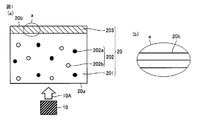
- FIG. 1A is a cross-sectional view schematically showing a light emitting device according to the first embodiment of the present invention
- FIG. 1B is an enlarged view of a region a in FIG.
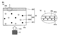
- FIG. 2A is a cross-sectional view schematically showing an example of a light emitting device according to the second embodiment of the present invention
- FIG. 2B is an enlarged view showing a region b in FIG. It is.
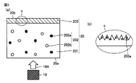
- FIG. 3A is a cross-sectional view schematically showing another example of the light emitting device according to the second embodiment of the present invention
- FIG. 3B is an enlarged view of a region c in FIG. FIG.
- It is sectional drawing which shows typically the light-emitting device which concerns on the 3rd Embodiment of this invention.
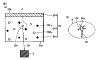
- FIG. 5A is a cross-sectional view schematically showing a light emitting device according to the fourth embodiment of the present invention
- FIG. 5B is an enlarged view of a region d in FIG. . It is a perspective view which shows typically the light-emitting device which concerns on the 5th Embodiment of this invention.
- FIG. 1A is a cross-sectional view schematically showing a light emitting device according to the present embodiment
- FIG. 1B is an enlarged view showing a region a in FIG.
- the light-emitting device shown in FIG. 1 is a light-emitting device that emits white light suitable as an illumination device, for example, and a light source 10 that emits primary light 10A and a second light that absorbs at least part of the primary light 10A and emits secondary light.
- the light emitting unit 20 including the translucent member 201 containing one nanoparticle 202.
- the first nanoparticle 202 includes a red semiconductor nanoparticle phosphor 202a and a green semiconductor nanoparticle phosphor 202b.
- the light emitting unit 20 is a light reflection preventing structure unit disposed on at least a part of the outer surface of the translucent member 201, specifically, on the outer surface from which the secondary light from the first nanoparticles 202 is emitted. 203.
- the light emitting unit 20 includes a light incident surface 20a on which the primary light 10A from the light source 10 is incident and a light emitting surface 20b on which the secondary light is emitted.
- the outer surface of the light reflection preventing structure 203 is a light emitting surface 20b.
- the light reflection preventing structure 203 is a layer (or member) that prevents or suppresses reflection of external light.
- the light reflection preventing structure 203 By providing the light reflection preventing structure 203, outside light is reflected by the light emitting surface 20b while ensuring the light transmitting property (visible light transmitting property) of the light emitting unit 20 when the light emitting device is not used. Since the reflection of light can be prevented or suppressed, the visibility when the light-emitting device is not used can be improved, and the light-emitting device can be made inconspicuous. Thereby, while being able to feel the surrounding space where a light-emitting device is installed widely, when using as an illuminating device etc., the interior property can also be improved.
- the light transmitting property visible light transmitting property
- the light source (excitation light source) 10 emits primary light 10 ⁇ / b> A absorbed by the first nanoparticles 202.
- the primary light 10 ⁇ / b> A has an emission peak wavelength that overlaps at least partially with the absorption wavelength of the first nanoparticle 202.
- a light source having an emission wavelength from the ultraviolet region to the blue region is usually used.
- a light emitting diode (LED) or a laser diode (LD) may be used. It can.
- an organic electroluminescence light emitting element, an inorganic electroluminescence light emitting element, etc. may be used.
- the LED or LD for example, a GaN-based LED or LD can be suitably used. Only one light source 10 may be used, or two or more light sources 10 may be used in combination.
- the translucent member 201 is a member in which the first nanoparticles 202 are contained and dispersed, in other words, a member that seals the first nanoparticles 202. At least a part of the outer surface of the translucent member 201 is a light incident surface 20a on which the primary light 10A from the light source 10 is incident, and the primary light 10A incident from the light incident surface 20a is at least one of the light incident surfaces 20a. The portion is absorbed by the first nanoparticles 202, whereby the first nanoparticles 202 emit light.
- the light emitting surface 20b of the light emitting unit 20 can be provided, for example, on the surface facing the light incident surface 20a.
- the translucent member 201 that can occupy most of the light emitting section 20 has translucency and is preferably transparent. This makes it possible to make the light emitting device translucent when not in use, which is advantageous in that the light emitting device is less noticeable.
- the term “transparent” means that the visible light transmittance is 90% or more.
- the material constituting the translucent member 201 is not particularly limited.
- a translucent (transparent) resin such as an acrylic resin or a silicone resin, a glass material, or the like can be used.
- acrylic resin for example, poly lauryl methacrylate etc.
- a semiconductor nanoparticle phosphor As the first nanoparticles 202 dispersed in the translucent member 201, a semiconductor nanoparticle phosphor can be used.
- the semiconductor nanoparticle phosphor is a nano-sized semiconductor material and exhibits a quantum confinement effect. When such quantum dots absorb primary light from the excitation source and reach an energy excited state, they emit energy corresponding to the energy band gap of the semiconductor nanoparticle phosphor. Therefore, by adjusting the particle size or material composition of the semiconductor nanoparticle phosphor, the energy band gap can be adjusted, and fluorescence of various wavelengths can be used.
- the semiconductor nanoparticle phosphor is a particle having a particle size in the range of 1 to 100 nm, more preferably 2 to 20 nm, and does not scatter visible light. Therefore, the translucency of the light emitting unit 20 when the light emitting device is not used. (Visibility of visible light) can be ensured.
- the present invention is not limited to this, and one type of semiconductor is used, for example, only yellow semiconductor nanoparticle phosphors are used. Only the nanoparticle phosphor may be used, or three or more kinds of semiconductor nanoparticle phosphors may be used.
- a semiconductor nanoparticle phosphor such as InP, InN, or CdSe can be preferably used. The type and combination of the semiconductor nanoparticle phosphors to be used are adjusted according to the desired hue of the secondary light emitted from the light emitting unit 20.
- the concentration of the first nanoparticles 202 dispersed in the translucent member 201 is usually 0.001 to 10% by weight when the total weight of the translucent member 201 and the first nanoparticles 202 is 100%.
- the content is 0.1 to 5% by weight.
- the light reflection preventing structure 203 is a layer (or member) that prevents or suppresses reflection of external light.
- the antireflection structure 203 is not particularly limited, and an antireflection layer having a multilayer structure of an optical thin film, a layer having irregularities on the surface (for example, a layer having a moth-eye structure), or the like can be suitably used.
- FIG. 1 shows an example using a multilayer structure of an optical thin film. Similar to the translucent member 201, the antireflection structure 203 is translucent and preferably transparent.
- an AG (Anti-Glare) film or an AR (Anti-Reflection) film can be used as the light reflection preventing structure 203.
- AG film particles are put into hard coat resin, and reflection is reflected by using the irregularities formed on the surface, and internal scattering due to refractive index difference between hard coat resin and particles is reflected. To prevent.
- the AR film is a film including an antireflection layer having a multilayer structure of optical thin films, and reduces the reflected light intensity using optical interference. Incident light is reflected at the surface of the antireflection layer and at the interface between the light emitting portion and the antireflection layer. In the AR film, the reflected light is canceled by reversing the phases of the surface reflected light and the interface reflected light. Can be reduced.
- the refractive index difference ⁇ n from the translucent member 201 to the air is also similar. Since it does not exist at the interface, the light extraction efficiency from the translucent member 201 to the outside (air) is improved. That is, the fluorescence extraction efficiency from the translucent member 201 to the outside (air) is improved.
- the shape of the protrusion constituting the surface concavo-convex structure is a cone shape, a pyramid shape, a bell shape, or the like depending on the formation conditions of the surface concavo-convex structure.
- Various shapes can be employed.
- the shape of the surface uneven structure is not particularly limited as long as it has a periodic structure having a wavelength of visible light or less.
- the surface uneven structure of the light antireflection structure 203 is provided. It is preferable to make the plane portion that can exist at the interface between the transparent member 201 and the translucent member 201 as small as possible.
- the arrangement position of the light reflection preventing structure 203 is not particularly limited as long as it is on at least a part of the outer surface of the translucent member 201, but at least the outer surface from which the secondary light from the first nanoparticles 202 is emitted. It is preferable to arrange on top. This is because the light emitting surface 20b is in a position where it is very easy to see in appearance, and the effect of the present invention (the prospect of the light emitting device) is very effectively prevented by preventing or suppressing the reflection of external light on the light emitting surface 20b. This is because it is possible to obtain an effect of improving the quality of the image and making it inconspicuous.
- the light reflection preventing structure 203 may be provided on the outer surface other than the outer surface from which the secondary light is emitted. More preferably, the light reflection preventing structure 203 is provided on the entire outer surface from which the secondary light is emitted.
- the side surfaces (outer surfaces other than the light incident surface 20a and the light emitting surface 20b) of the translucent member 201 are not shown.
- the side surface of the coated translucent member 201 does not reflect outside light, the light reflection preventing structure 203 is not necessarily provided.
- the light emitting surface 20b of the light emitting unit 20 is not necessarily provided on the surface facing the light incident surface 20a, and is formed on the side surface of the translucent member 201 instead of or together with the surface. May be.
- the shape of the light emitting unit 20 is not particularly limited, and may be, for example, a complicated three-dimensional shape such as an animal or a doll in addition to a geometric three-dimensional shape such as a cube, a rectangular parallelepiped, a sphere, or a cone.
- FIG. 2A is a cross-sectional view schematically showing an example of the light emitting device according to the present embodiment
- FIG. 2B is an enlarged view of a region b in FIG.
- the light-emitting device shown in FIG. 2 is not limited to the fact that the translucent member 201 contains the first nanoparticles 202, and the light reflection preventing structure 203 further contains the second nanoparticles 203a. This is the same as the embodiment.
- the second nanoparticles 203a are made of ultraviolet light-absorbing nanoparticles.
- the ultraviolet light absorbing second nanoparticles 203a include doped and core / shell type nanoparticles such as InAs / ZnS, InAs / ZnO, InAs / TiO 2 , ZnO: Mg, ZnO: Be, GaN, ZnS.
- inorganic phosphor nanoparticles such as YVO 4 can be used.
- the 2nd nanoparticle 203a may consist only of 1 type of nanoparticle, and may consist of 2 or more types of nanoparticles.
- the first nanoparticles 202 and the second nanoparticles 203a may be made of the same material or different materials.
- the first nanoparticle 202 and the second nanoparticle 203a may have the same particle size or different particle sizes.
- a red semiconductor nanoparticle phosphor 202a and a green semiconductor nanoparticle phosphor 202b are used as the first nanoparticles 202, and a blue semiconductor nanoparticle phosphor is used as the second nanoparticles 203a.
- a blue semiconductor nanoparticle phosphor is used as the second nanoparticles 203a.
- the short-wavelength light can enter the translucent member 201 by providing the light reflection preventing structure 203.
- the translucent member 201 and the first nanoparticles 202 included therein may be deteriorated by the short wavelength light.
- the second nanoparticle 203a is contained and dispersed in the light reflection preventing structure portion 203, short wavelength light such as ultraviolet light in external light is absorbed by the second nanoparticle 203a. The Therefore, it is possible to prevent short wavelength light from entering the inside of the translucent member 201, thereby preventing deterioration of the translucent member 201 and the first nanoparticles 202 included therein.
- the second nanoparticles 203a are dispersed throughout the entire surface of the light reflection preventing structure 203.
- the second nanoparticles 203a may be dispersed throughout the entire thickness direction of the light reflection preventing structure 203 or may be partially dispersed.
- FIG. 3A is a cross-sectional view schematically showing another example of the light emitting device according to the present embodiment
- FIG. 3B is an enlarged view of a region c in FIG.
- the light emitting device shown in FIG. 3 is an example in which a layer having irregularities on the surface is used as the light reflection preventing structure 203, and the second nanoparticles 203a are dispersed on the convexities of the irregular surface structure. Even with such a configuration, the same effect as that of the light-emitting device shown in FIG. 2 can be obtained.
- the second nanoparticles 203a are dispersed in the convex portions of the surface concavo-convex structure, the surface area that comes into contact with air increases, so that improvement in heat dissipation of the light emitting device can be expected.
- the second nanoparticles 203a may of course be dispersed in portions other than the convex portions of the light reflection preventing structure portion 203.
- FIG. 4 is a cross-sectional view schematically showing the light emitting device according to this embodiment.
- the light emitting device shown in FIG. 4 uses, as the second nanoparticle 203b contained in the light reflection preventing structure portion 203, a nanoparticle that absorbs ultraviolet light and emits visible light by absorbing ultraviolet light.
- the second embodiment is the same as the second embodiment.
- a doped or core / shell type semiconductor nanoparticle phosphor such as CdSe / ZnS, CdSe / ZnO, CdSe / TiO 2 , CdS / ZnS, CdS / ZnO, CdS / TiO 2 , ZnSe / ZnS, ZnSe / ZnO, ZnSe / TiO 2 , InP / GaN, InP / ZnS, InP / ZnO, InP / TiO 2 , preferably InN / GaN, InN / ZnS, Wide-gap semiconductor nanoparticle phosphors such as InN / ZnO and InN / TiO 2 ;
- inorganic phosphor nanoparticles such as YVO 4 : Bi 3+ , Eu 3+ and YVO 4 : Eu 3+ can be used.
- the second nanoparticle 203b may be composed of only one kind of nanoparticle or may be composed of two or more kinds of nanoparticles.
- the first nanoparticles 202 and the second nanoparticles 203b may be made of the same material or different materials.
- the first nanoparticle 202 and the second nanoparticle 203b may have the same particle size or different particle sizes.
- An example of a preferable combination of phosphor particles to be used is a red semiconductor nanoparticle phosphor 202a and a green semiconductor nanoparticle phosphor 202b as the first nanoparticle 202, and a blue semiconductor nanoparticle phosphor as the second nanoparticle 203b. Is to use. In this case, when the light emitting device is used, red light and green light emitted from the first nanoparticles 202 are not absorbed by the second nanoparticles 203b, so that there is no adverse effect on the hue and luminance, for example, in lighting applications.
- the same effects as those of the second embodiment can be obtained, and when the light reflection preventing structure portion 203 is irradiated with external light, even when the light emitting device is not used.
- the light emitting unit 20 (light reflection preventing structure unit 203) can emit light weakly. This is advantageous in that it is possible to provide a lighting device with high decorativeness, and it is easy to avoid a collision with the lighting device.
- FIG. 5A is a cross-sectional view schematically showing the light emitting device according to the present embodiment
- FIG. 5B is an enlarged view of a region d in FIG.
- the light-emitting device shown in FIG. 5 is a modification of the light-emitting device according to the first embodiment.
- the surface of the translucent member 201 facing the light source 10 is a light incident surface 20a, and primary light is directed toward the light incident surface 20a.
- the light source 10 and the inside of the translucent member 201 are connected by the light guide member 30, and the primary light 10A is transmitted to the inside of the translucent member 201. It is said.
- the light incident surface 20a exists inside the translucent member 201.
- an optical fiber or the like can be used as the light guide member 30.
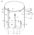
- FIG. 6 is a perspective view schematically showing the light emitting device according to this embodiment.
- the light emitting section 20 has a cylindrical shape, and not only a flat outer surface facing the light incident surface but also a curved outer surface (side surface) is a light emitting surface.
- the light reflection preventing structure 203 is arranged on the flat outer surface and the curved outer surface, and is the same as the fifth embodiment.
- the outer shape of the light emitting unit 20 is not particularly limited, and may be various shapes such as a rectangular shape such as a cube and a rectangular parallelepiped, and a cylindrical shape. Regardless of the outer shape of the light emitting unit 20, it is preferable to dispose the light reflection preventing structure unit 203 on at least the outer surface from which the secondary light from the first nanoparticles 202 is emitted.
- 10 light source 10A primary light, 20 light emitting part, 20a light incident surface, 20b light emitting surface, 30 light guide member, 201 translucent member, 202 first nanoparticle, 202a red semiconductor nanoparticle phosphor, 202b green semiconductor nano Particle phosphor, 203, light reflection preventing structure, 203a, 203b second nanoparticles.
Landscapes
- Physics & Mathematics (AREA)
- Engineering & Computer Science (AREA)
- General Engineering & Computer Science (AREA)
- Optics & Photonics (AREA)
- General Physics & Mathematics (AREA)
- Spectroscopy & Molecular Physics (AREA)
- Chemical & Material Sciences (AREA)
- Dispersion Chemistry (AREA)
- Microelectronics & Electronic Packaging (AREA)
- Inorganic Chemistry (AREA)
- Led Device Packages (AREA)
Abstract
Description
[1] 一次光を発する光源と、
前記一次光の少なくとも一部を吸収して二次光を発する第1ナノ粒子を含有する透光性部材を備える発光部と、
を含み、
前記発光部は、前記透光性部材の少なくとも一部の外表面上に配置される光反射防止構造部を備える、発光装置。
前記一次光は、前記透光性部材の内部に伝送される、[1]~[3]のいずれかに記載の発光装置。
<第1の実施形態>
図1(a)は本実施形態に係る発光装置を模式的に示す断面図であり、図1(b)は図1(a)における領域aを拡大して示す図である。図1に示される発光装置は、例えば照明装置として好適な白色光を発する発光装置であり、一次光10Aを発する光源10と、一次光10Aの少なくとも一部を吸収して二次光を発する第1ナノ粒子202を含有する透光性部材201を備える発光部20とを含む。図1に示される発光装置において、第1ナノ粒子202は、赤色半導体ナノ粒子蛍光体202a及び緑色半導体ナノ粒子蛍光体202bからなる。
光源(励起光源)10は、第1ナノ粒子202が吸収する一次光10Aを発するものである。一次光10Aは、第1ナノ粒子202の吸収波長と少なくとも一部において重複する発光ピーク波長を有する。このような一次光10Aを発する光源10として、通常は、紫外領域から青色領域までの発光波長を有する光源が使用され、例えば、発光ダイオード(LED)やレーザーダイオード(LD)などを使用することができる。また、有機エレクトロルミネッセンス発光素子や無機エレクトロルミネッセンス発光素子などを使用してもよい。LEDやLDとして、例えば、GaN系LEDやLDを好適に用いることができる。光源10は1個のみを用いてもよく、2個以上を併用してもよい。
透光性部材201は、第1ナノ粒子202が含有・分散される部材であり、換言すれば、第1ナノ粒子202を封止する部材である。透光性部材201の外表面の少なくとも一部は、光源10からの一次光10Aが入射される光入射面20aとなっており、光入射面20aから入射された一次光10Aは、その少なくとも一部が第1ナノ粒子202によって吸収され、これにより第1ナノ粒子202が発光する。発光部20の光出射面20bは、例えば、光入射面20aに対向する面側に設けることができる。
光反射防止構造部203は、外光の反射を防止又は抑制する層(又は部材)である。光反射防止構造部203としては、特に制限されないが、光学薄膜の多層構造からなる反射防止層や、表面に凹凸を有する層(例えば、モスアイ構造を有する層等)などを好適に用いることができる。図1は、光学薄膜の多層構造を用いた例である。光反射防止構造部203は、透光性部材201と同様、透光性であり、好ましくは透明である。
n1 2=n0×n2 (1)
〔n0は反射防止層の外部領域の屈折率である。〕
n1×d1=λ/4 (2)
を満たす場合、波長λ(nm)における反射率が0%となる。式(2)から、反射防止効果は波長依存性があり、反射防止層の膜厚依存性もあることがわかる。
R=〔(n1-n2)2/(n1+n2)2〕×100 (3)
で表わされる。
図2(a)は本実施形態に係る発光装置の一例を模式的に示す断面図であり、図2(b)は図2(a)における領域bを拡大して示す図である。図2に示される発光装置は、透光性部材201が第1ナノ粒子202を含有するだけでなく、さらに光反射防止構造部203が第2ナノ粒子203aを含有すること以外は、上記第1の実施形態と同様である。
図4は、本実施形態に係る発光装置を模式的に示す断面図である。図4に示される発光装置は、光反射防止構造部203に含有される第2ナノ粒子203bとして、紫外光吸収性であって、かつ、紫外光の吸収により可視光を発するナノ粒子を用いること以外は、上記第2の実施形態と同様である。
図5(a)は本実施形態に係る発光装置を模式的に示す断面図であり、図5(b)は図5(a)における領域dを拡大して示す図である。図5に示される発光装置は、上記第1の実施形態に係る発光装置の変形例であり、透光性部材201における光源10に対向する表面を光入射面20aとし、そこに向けて一次光10Aを照射する第1の実施形態とは異なり、光源10と透光性部材201の内部とを導光部材30で接続し、一次光10Aを透光性部材201の内部に伝送することを特徴としている。
図6は、本実施形態に係る発光装置を模式的に示す斜視図である。図6に示される発光装置は、発光部20が円柱形状を有しており、光入射面に対向する平面状の外表面だけでなく、曲面となっている外表面(側面)も光出射面となっていて、該平面状の外表面及び曲面となっている外表面に光反射防止構造部203を配置していること以外は、上記第5の実施形態と同様である。
Claims (5)
- 一次光を発する光源と、
前記一次光の少なくとも一部を吸収して二次光を発する第1ナノ粒子を含有する透光性部材を備える発光部と、
を含み、
前記発光部は、前記透光性部材の少なくとも一部の外表面上に配置される光反射防止構造部を備える、発光装置。 - 前記光反射防止構造部は、紫外光吸収性の第2ナノ粒子を含有する、請求項1に記載の発光装置。
- 前記第2ナノ粒子は、紫外光を吸収することにより可視光を発するナノ粒子蛍光体である、請求項2に記載の発光装置。
- 前記光源と前記透光性部材とは導光部材によって接続されており、
前記一次光は、前記透光性部材の内部に伝送される、請求項1~3のいずれか1項に記載の発光装置。 - 前記透光性部材における、少なくとも前記二次光が出射される外表面上に前記光反射防止構造部が配置される、請求項1~4のいずれか1項に記載の発光装置。
Priority Applications (2)
| Application Number | Priority Date | Filing Date | Title |
|---|---|---|---|
| US14/891,095 US20160109073A1 (en) | 2013-05-28 | 2014-02-18 | Light-emitting device |
| JP2015519688A JP6133982B2 (ja) | 2013-05-28 | 2014-02-18 | 発光装置 |
Applications Claiming Priority (2)
| Application Number | Priority Date | Filing Date | Title |
|---|---|---|---|
| JP2013-111855 | 2013-05-28 | ||
| JP2013111855 | 2013-05-28 |
Publications (1)
| Publication Number | Publication Date |
|---|---|
| WO2014192333A1 true WO2014192333A1 (ja) | 2014-12-04 |
Family
ID=51988378
Family Applications (1)
| Application Number | Title | Priority Date | Filing Date |
|---|---|---|---|
| PCT/JP2014/053727 Ceased WO2014192333A1 (ja) | 2013-05-28 | 2014-02-18 | 発光装置 |
Country Status (3)
| Country | Link |
|---|---|
| US (1) | US20160109073A1 (ja) |
| JP (1) | JP6133982B2 (ja) |
| WO (1) | WO2014192333A1 (ja) |
Cited By (1)
| Publication number | Priority date | Publication date | Assignee | Title |
|---|---|---|---|---|
| TWI707200B (zh) * | 2015-09-29 | 2020-10-11 | 德商馬克專利公司 | 光敏組合物及色轉變膜、彼等之應用以及製備方法 |
Families Citing this family (1)
| Publication number | Priority date | Publication date | Assignee | Title |
|---|---|---|---|---|
| JP2018111764A (ja) * | 2017-01-11 | 2018-07-19 | シャープ株式会社 | 波長変換部材および発光装置 |
Citations (3)
| Publication number | Priority date | Publication date | Assignee | Title |
|---|---|---|---|---|
| JP2006253099A (ja) * | 2005-02-08 | 2006-09-21 | Nichia Chem Ind Ltd | 発光装置 |
| JP2007035885A (ja) * | 2005-07-26 | 2007-02-08 | Kyocera Corp | 発光装置およびそれを用いた照明装置 |
| JP2008021578A (ja) * | 2006-07-14 | 2008-01-31 | Koito Mfg Co Ltd | 車両用標識灯 |
Family Cites Families (10)
| Publication number | Priority date | Publication date | Assignee | Title |
|---|---|---|---|---|
| JPH0684487U (ja) * | 1993-05-17 | 1994-12-02 | 株式会社ヤマウ | 発光標識体 |
| US7088040B1 (en) * | 2002-06-27 | 2006-08-08 | University Of Central Florida Research Foundation, Inc. | Light source using emitting particles to provide visible light |
| US7497581B2 (en) * | 2004-03-30 | 2009-03-03 | Goldeneye, Inc. | Light recycling illumination systems with wavelength conversion |
| KR100682874B1 (ko) * | 2005-05-02 | 2007-02-15 | 삼성전기주식회사 | 백색 led |
| US7446939B2 (en) * | 2005-12-22 | 2008-11-04 | Guardian Industries Corp. | Optical diffuser with UV blocking coating using inorganic materials for blocking UV |
| KR20110080165A (ko) * | 2008-10-17 | 2011-07-12 | 루미너스 디바이시즈, 아이엔씨. | 원격 조명 조립체 및 방법 |
| JP5375424B2 (ja) * | 2009-08-10 | 2013-12-25 | 東芝ライテック株式会社 | 発光装置及びその製造方法、灯具、並びに灯具システム |
| JP4991001B2 (ja) * | 2009-12-28 | 2012-08-01 | シャープ株式会社 | 照明装置 |
| JP2011252117A (ja) * | 2010-06-03 | 2011-12-15 | Sharp Corp | 半導体微粒子蛍光体、ならびにそれを用いた波長変換部材、発光装置および画像表示装置 |
| JP5181045B2 (ja) * | 2011-06-21 | 2013-04-10 | シャープ株式会社 | 発光装置、照明装置、車両用前照灯 |
-
2014
- 2014-02-18 WO PCT/JP2014/053727 patent/WO2014192333A1/ja not_active Ceased
- 2014-02-18 US US14/891,095 patent/US20160109073A1/en not_active Abandoned
- 2014-02-18 JP JP2015519688A patent/JP6133982B2/ja not_active Expired - Fee Related
Patent Citations (3)
| Publication number | Priority date | Publication date | Assignee | Title |
|---|---|---|---|---|
| JP2006253099A (ja) * | 2005-02-08 | 2006-09-21 | Nichia Chem Ind Ltd | 発光装置 |
| JP2007035885A (ja) * | 2005-07-26 | 2007-02-08 | Kyocera Corp | 発光装置およびそれを用いた照明装置 |
| JP2008021578A (ja) * | 2006-07-14 | 2008-01-31 | Koito Mfg Co Ltd | 車両用標識灯 |
Cited By (1)
| Publication number | Priority date | Publication date | Assignee | Title |
|---|---|---|---|---|
| TWI707200B (zh) * | 2015-09-29 | 2020-10-11 | 德商馬克專利公司 | 光敏組合物及色轉變膜、彼等之應用以及製備方法 |
Also Published As
| Publication number | Publication date |
|---|---|
| US20160109073A1 (en) | 2016-04-21 |
| JPWO2014192333A1 (ja) | 2017-02-23 |
| JP6133982B2 (ja) | 2017-05-24 |
Similar Documents
| Publication | Publication Date | Title |
|---|---|---|
| RU2634699C1 (ru) | Светоизлучающий модуль, лампа, светильник и способ освещения объекта | |
| JP5286393B2 (ja) | 発光素子、発光装置および発光素子の製造方法 | |
| TWI497167B (zh) | 直下式背光模組及其光源擴散結構 | |
| JP6727483B2 (ja) | 照明装置のカラーフィルター用材料および光学部品 | |
| JP6622187B2 (ja) | 波長変換部材、導光装置、並びに表示装置 | |
| JP6185987B2 (ja) | 発光装置 | |
| CN104272018B (zh) | 用于提供中性颜色外观的照明组件、灯具和照明装置 | |
| JP6339007B2 (ja) | カラー外観が低減された蛍光体増強照明装置、レトロフィット電球及び管電球 | |
| TWI520383B (zh) | 發光二極體封裝結構 | |
| JP2011007995A (ja) | スクリーンおよびプロジェクションシステム | |
| JP6133982B2 (ja) | 発光装置 | |
| JP6644233B2 (ja) | 発光装置 | |
| US7314292B2 (en) | Lighting device | |
| KR20190087482A (ko) | 필터를 포함하는 이색성 산화 아연 나노로드를 이용해 전기-발광 광원의 발산을 증강시키는 광학 디바이스 | |
| CN209042245U (zh) | 灯具 | |
| CN209146979U (zh) | 灯具 | |
| CN209042236U (zh) | 灯具 | |
| CN209042237U (zh) | 灯具 | |
| US20200041101A1 (en) | Wavelength conversion film | |
| CN109616565B (zh) | 灯具 | |
| JP2016012605A (ja) | 発光装置 | |
| TW201304209A (zh) | 降低色彩外觀之磷光體增強照明裝置、改裝燈泡及燈管 |
Legal Events
| Date | Code | Title | Description |
|---|---|---|---|
| 121 | Ep: the epo has been informed by wipo that ep was designated in this application |
Ref document number: 14804160 Country of ref document: EP Kind code of ref document: A1 |
|
| ENP | Entry into the national phase |
Ref document number: 2015519688 Country of ref document: JP Kind code of ref document: A |
|
| WWE | Wipo information: entry into national phase |
Ref document number: 14891095 Country of ref document: US |
|
| NENP | Non-entry into the national phase |
Ref country code: DE |
|
| 122 | Ep: pct application non-entry in european phase |
Ref document number: 14804160 Country of ref document: EP Kind code of ref document: A1 |