WO2014192245A1 - 多結晶シリコン中の局所配向ドメインの評価方法 - Google Patents
多結晶シリコン中の局所配向ドメインの評価方法 Download PDFInfo
- Publication number
- WO2014192245A1 WO2014192245A1 PCT/JP2014/002609 JP2014002609W WO2014192245A1 WO 2014192245 A1 WO2014192245 A1 WO 2014192245A1 JP 2014002609 W JP2014002609 W JP 2014002609W WO 2014192245 A1 WO2014192245 A1 WO 2014192245A1
- Authority
- WO
- WIPO (PCT)
- Prior art keywords
- polycrystalline silicon
- sample
- diffraction intensity
- plate
- silicon rod
- Prior art date
- Legal status (The legal status is an assumption and is not a legal conclusion. Google has not performed a legal analysis and makes no representation as to the accuracy of the status listed.)
- Ceased
Links
Images







Classifications
-
- G—PHYSICS
- G01—MEASURING; TESTING
- G01N—INVESTIGATING OR ANALYSING MATERIALS BY DETERMINING THEIR CHEMICAL OR PHYSICAL PROPERTIES
- G01N23/00—Investigating or analysing materials by the use of wave or particle radiation, e.g. X-rays or neutrons, not covered by groups G01N3/00 – G01N17/00, G01N21/00 or G01N22/00
- G01N23/20—Investigating or analysing materials by the use of wave or particle radiation, e.g. X-rays or neutrons, not covered by groups G01N3/00 – G01N17/00, G01N21/00 or G01N22/00 by using diffraction of the radiation by the materials, e.g. for investigating crystal structure; by using scattering of the radiation by the materials, e.g. for investigating non-crystalline materials; by using reflection of the radiation by the materials
-
- G—PHYSICS
- G01—MEASURING; TESTING
- G01N—INVESTIGATING OR ANALYSING MATERIALS BY DETERMINING THEIR CHEMICAL OR PHYSICAL PROPERTIES
- G01N2223/00—Investigating materials by wave or particle radiation
- G01N2223/60—Specific applications or type of materials
- G01N2223/602—Specific applications or type of materials crystal growth
-
- G—PHYSICS
- G01—MEASURING; TESTING
- G01N—INVESTIGATING OR ANALYSING MATERIALS BY DETERMINING THEIR CHEMICAL OR PHYSICAL PROPERTIES
- G01N2223/00—Investigating materials by wave or particle radiation
- G01N2223/60—Specific applications or type of materials
- G01N2223/604—Specific applications or type of materials monocrystal
-
- G—PHYSICS
- G01—MEASURING; TESTING
- G01N—INVESTIGATING OR ANALYSING MATERIALS BY DETERMINING THEIR CHEMICAL OR PHYSICAL PROPERTIES
- G01N2223/00—Investigating materials by wave or particle radiation
- G01N2223/60—Specific applications or type of materials
- G01N2223/606—Specific applications or type of materials texture
Definitions
- the present invention relates to a method for evaluating local orientation domains contained in polycrystalline silicon, and a polycrystalline silicon rod or polycrystalline silicon lump suitable as a raw material for stably producing single crystal silicon using the method. Relates to the method of selecting.
- Siemens method is a method of vapor deposition (deposition) of polycrystalline silicon on the surface of silicon core wire by CVD (Chemical Vapor Deposition) method by bringing silane source gas such as trichlorosilane and monosilane into contact with heated silicon core wire. It is a method to make it.
- Patent Document 2 discloses that needle-like crystals may be precipitated in a rod during the process of manufacturing a polycrystalline silicon rod (polycrystalline silicon rod) by the Siemens method.
- the melting of individual crystallites depends on their size, so they do not melt uniformly, and unmelted crystallites pass through the melting zone as solid particles into single crystal rods.
- defects are formed as a result of being incorporated into the solidified surface of the single crystal as unmelted particles.
- Patent Document 2 the sample surface cut perpendicularly to the long axis direction of the polycrystalline silicon rod is polished or polished, and after etching, the microcrystals of the structure are contrasted to such an extent that they can be visually recognized under an optical microscope.
- the present invention has been made in view of such problems, and the object of the present invention is to select polycrystalline silicon suitable as a raw material for producing single crystal silicon with high quantitativeness and reproducibility. It is to provide a technology that contributes to stable manufacturing.
- a method for evaluating a local orientation domain in polycrystalline silicon is a method for evaluating a local orientation domain contained in polycrystalline silicon by an X-ray diffraction method.
- Crystal silicon is used as a plate-like sample, the plate-like sample is arranged at a position where Bragg reflection from the mirror index surface ⁇ hkl> is detected, and an X-ray irradiation region defined by a slit is on the main surface of the plate-like sample.
- the Miller index surface ⁇ hkl> is at least one of ⁇ 111> and ⁇ 220>.
- a method for selecting a polycrystalline silicon rod according to the present invention is a method for selecting a polycrystalline silicon rod used as a raw material for producing single crystal silicon by an X-ray diffraction method, wherein the polycrystalline silicon rod is a chemical vapor phase method.
- a plate-like sample having a cross section perpendicular to the radial direction of the polycrystalline silicon rod as a main surface is collected, and the plate-like sample is subjected to Bragg reflection from the mirror index surface ⁇ hkl>.
- the Miller index surface ⁇ hkl> is at least one of ⁇ 111> and ⁇ 220>.
- the diffraction intensity ratio R 111 is 1.8 or less and the diffraction intensity ratio R 220 is 12 or less, it is selected as a polycrystalline silicon rod used as a raw material for producing single crystal silicon.
- the polycrystalline silicon rod is grown by the Siemens method.
- the polycrystalline silicon rod selected by the method of the present invention a random crystalline orientation state is realized even locally, and there are very few or no local orientation domains that are likely to be unmelted particles in the silicon melt. . For this reason, when a single crystal is grown by the FZ method using such a polycrystalline silicon rod, or a single crystal is grown by the CZ method using a polycrystalline silicon lump obtained by crushing such a polycrystalline silicon rod. The occurrence of a local unmelted state is suppressed, and stable production of single crystal silicon becomes possible.
- FIG. 5 is an example of a chart obtained by performing the ⁇ scan measurement shown in FIG. 4 for the mirror index surfaces ⁇ 111>, ⁇ 220>, ⁇ 311>, and ⁇ 400>. It is a figure for demonstrating the outline of the other example of a measurement system at the time of calculating
- 7 is an example of a chart obtained by performing the ⁇ scan measurement shown in FIG.
- polycrystalline silicon Unlike single crystal silicon, polycrystalline silicon consists of a myriad of grains, and generally the size of individual grains is approximately a few microns to a few tens of microns, and usually the individual grains are randomly oriented relative to each other. It is thought that However, when examined in detail, there are cases where regions oriented in substantially the same crystal orientation are recognized in polycrystalline silicon, and the size is as large as several millimeters.
- the crystal axes are locally aligned in a specific orientation. Some areas may exist. In other words, even if the crystal grains are randomly oriented when viewed macroscopically, there can be polycrystalline silicon in which there are not necessarily randomly oriented regions when viewed microscopically.
- Such a local orientation region may be a so-called “crystal domain” (region consisting of a single crystal), or a region formed by a plurality of crystal grains in which individual crystal orientations are substantially the same. In other words, it may be a pseudo “crystal domain”.
- the present inventor is able to evaluate the local orientation domain by X-ray diffraction in the course of studying a method for selecting a polycrystalline silicon rod or a polycrystalline silicon lump suitable for stable production of single crystal silicon. I came to know that there is. In particular, the peaks from the Miller index planes ⁇ 111> and ⁇ 220> have been found to be effective in evaluating the local orientation domain.
- an example of collecting a plate sample for X-ray diffraction measurement from a polycrystalline silicon rod grown by chemical vapor deposition an X-ray diffraction profile from the plate sample is represented by ⁇ .
- Outline of measurement system example for obtaining by -2 ⁇ method outline of measurement system example for obtaining X-ray diffraction profile from plate-like sample by ⁇ scan method, ⁇ scan measurement for mirror index surface ⁇ 111>, ⁇ 220> , ⁇ 311>, ⁇ 400> are described, and examples of peaks appearing on the ⁇ scan chart for the mirror index surfaces ⁇ 111> and ⁇ 220> of the plate-like sample are described. To do.
- FIGS. 1A and 1B are diagrams for explaining an example of collecting a plate-like sample 20 for measuring an X-ray diffraction profile from a polycrystalline silicon rod 10 grown by chemical vapor deposition such as Siemens method. It is.
- reference numeral 1 denotes a silicon core wire for depositing polycrystalline silicon on the surface to form a silicon rod.
- CTR part close to the silicon core wire 1
- EDG part to confirm whether or not the degree of crystal orientation of the polycrystalline silicon rod 10 (the degree of the presence of local orientation domains) is dependent on the radial direction).
- the plate-like sample 20 is collected from a portion close to the side surface of the polycrystalline silicon rod 10 (R / 2: intermediate portion between CTR and EGD), but is not limited to collection from such a portion.
- the diameter of the polycrystalline silicon rod 10 illustrated in FIG. 1A is approximately 120 mm. From the side surface side of the polycrystalline silicon rod 10, a rod 11 having a diameter of approximately 20 mm and a length of approximately 60 mm is connected to the longitudinal direction of the silicon core wire 1. And cut out vertically.
- the portion, length, and number of the rods 11 to be collected may be determined as appropriate according to the diameter of the silicon rod 10 or the diameter of the rod 11 to be hollowed out. However, it is preferable that the position of the silicon rod 10 as a whole can be reasonably estimated.
- the position on the center side and the position on the outside of the point that is half the radius from the center with respect to the radius of the circumference of the silicon rod is preferable to obtain a disk-shaped sample from two places.
- the acquisition positions of two samples to be compared are located on the center side of a point that is one third of the radius from the center and outside the point that is two thirds of the radius from the center. If the position is used, a more accurate comparison can be made.
- the disk-shaped sample to be compared should just be 1 or more, and there is no upper limit in particular.
- the diameter of the disk-shaped sample 20 is set to approximately 20 mm for illustration only, and the diameter may be appropriately determined within a range that does not hinder the X-ray diffraction measurement.
- the plate-like sample 20 collected as described above is placed at a position where Bragg reflection from the mirror index surface ⁇ hkl> is detected.
- the mirror index plane is arranged and rotated in-plane at a rotation angle ⁇ around the center of the plate-like sample 20 so that the X-ray irradiation area defined by the slit scans the main surface of the plate-like sample 20 ⁇ . From the chart, a peak top diffraction intensity value and a baseline diffraction intensity value are obtained.
- the peaks from the Miller index planes ⁇ 111> and ⁇ 220> are particularly effective for the evaluation of the local orientation domain.
- hkl> is preferably at least one of ⁇ 111> and ⁇ 220>.
- the above-described method for evaluating the local orientation domain of polycrystalline silicon is used to select a polycrystalline silicon rod used as a raw material for producing single crystal silicon by the X-ray diffraction method.
- the method for selecting a polycrystalline silicon rod according to the present invention is a method for selecting a polycrystalline silicon rod used as a raw material for producing single crystal silicon by an X-ray diffraction method.
- a plate-like sample which is grown by precipitation by a phase method and has a cross section perpendicular to the radial direction of the polycrystalline silicon rod as a main surface, and the Bragg sample from the Miller index surface ⁇ hkl> It is placed at a position where reflection is detected, and the X-ray irradiation area defined by the slit rotates in-plane at a rotation angle ⁇ around the center of the plate sample as the rotation center so that the main surface of the plate sample is ⁇ scanned
- the peak top diffraction intensity value and the baseline diffraction intensity value are obtained. Therefore, the value obtained by dividing the diffraction intensity value
- the Miller index surface ⁇ hkl> is preferably at least one of ⁇ 111> and ⁇ 220>.
- FIG. 2 is a diagram for explaining an outline of an example of a measurement system when an X-ray diffraction profile from the disk-shaped sample 20 is obtained by a so-called ⁇ -2 ⁇ method.
- the collimated X-ray beam 40 (Cu-K ⁇ ray: wavelength 1.54 mm) emitted from the slit 30 is incident on the disk-shaped sample 20 and rotates the sample while rotating the disk-shaped sample 20 in the XY plane.
- the intensity of the diffracted X-ray beam for each angle ( ⁇ ) is detected by a detector (not shown) to obtain an X-ray diffraction chart of ⁇ -2 ⁇ .
- FIG. 4 is a diagram for explaining an outline of a measurement system when an X-ray diffraction profile from the disk-shaped sample 20 is obtained by a so-called ⁇ scan method.
- the angle ⁇ of the disk-shaped sample 20 is set to an angle at which Bragg reflection from the mirror index surface ⁇ 111> is detected, and in this state, a slit is defined in a region extending from the center of the disk-shaped sample 20 to the peripheral edge.
- FIG. 5 is an example of a chart obtained by performing the ⁇ scan measurement on the mirror index surfaces ⁇ 111>, ⁇ 220>, ⁇ 311>, and ⁇ 400>.
- the Bragg reflection intensity is substantially constant regardless of any of the above Miller index surfaces, and the Bragg reflection intensity does not depend on the rotation angle ⁇ , and is the same chart as the powder sample. That is, it can be determined that this disk-shaped sample 20 does not have a local alignment domain.
- FIG. 6 is a diagram for explaining an outline of another measurement system example for obtaining an X-ray diffraction profile from the disk-shaped sample 20 by the ⁇ scan method.
- the disk-shaped sample is illustrated.
- An area extending across both ends of 20 is irradiated with X-rays on a thin rectangular area defined by a slit, and the center of the disk-shaped sample 20 is scanned so that this X-ray irradiation area scans the entire surface of the disk-shaped sample 20.
- Rotate in the YZ plane ( ⁇ 0 ° to 180 °) as the center of rotation.
- FIG. 7 is an example of a chart obtained by performing the above ⁇ scan measurement on the mirror index surfaces ⁇ 111>, ⁇ 220>, ⁇ 311>, ⁇ 400>, which is substantially the same as that shown in FIG. The same ⁇ scan chart is obtained.
- FIG. 8 is a diagram for explaining an outline of another example of a measurement system when an X-ray diffraction profile from the disk-shaped sample 20 is obtained by the ⁇ scan method.
- X-rays are irradiated not on the entire main surface of the sample 20 but only on the inner peripheral region, and the center of the disk-shaped sample 20 is set as the center of rotation so that this X-ray irradiation region scans the entire surface of the disk-shaped sample 20.
- FIGS. 9A and 9B are an example of a ⁇ scan chart for the mirror index surface ⁇ 111> of a plate sample taken from the center of the polycrystalline silicon rod, and a plate taken from the outer periphery of the polycrystalline silicon rod, respectively. It is an example of a ⁇ scan chart about the mirror index surface ⁇ 220> of the sample.
- FIG. 10 is a diagram for explaining how to define a peak appearing in the ⁇ scan chart for the mirror index surface ⁇ hkl> of the plate-like sample.
- the crystal is oriented completely at random, so that the diffraction intensity from a specific mirror index surface ⁇ hkl> is constant, so that the “baseline” diffraction intensity should be generally constant even when ⁇ scan is performed. . However, if a local alignment domain exists, a peak appears, and the “baseline” becomes “noise”.
- the present inventor has determined whether or not there is a peak in the ⁇ scan chart, for example, the average value of the diffraction intensity values of the upper limit value B H and the lower limit value B L of the “baseline” in the vicinity of the “peak”.
- the “peak” is adopted as a peak for local alignment domain evaluation.
- the ratio (R 220 ) is obtained, and when the diffraction intensity ratio R 111 is 1.8 or less and the diffraction intensity ratio R 220 is 12 or less, it is selected as a polycrystalline silicon rod used as a raw material for producing single crystal silicon. It is preferable.
- processing such as obtaining a difference between the ⁇ scan chart obtained from the X-ray irradiation region as shown in FIG. 8 and the ⁇ scan chart obtained from the entire main surface of the disk-shaped sample 20 is performed. It is also possible to obtain a distribution of local orientation domains in the plane of the disk-shaped sample 20.
- the evaluation of the local orientation domain according to the present invention is as follows. Needless to say, it is significant not only as a method for selecting a polycrystalline silicon rod grown by the Siemens method or the like, but also as a method for evaluating the whole polycrystalline silicon by the X-ray diffraction method.
- the inside of the polycrystalline silicon rod It is also possible to know the presence / absence of a local orientation domain in the region and the change of the local orientation domain accompanying the enlargement of the diameter of the polycrystalline silicon rod, which makes it possible to select a polycrystalline silicon rod suitable as a raw material for producing single crystal silicon. It becomes possible.
- the presence or absence of the local orientation domain in the polycrystalline silicon is evaluated by the above-described method, and the polycrystalline silicon rod or the polycrystalline silicon rod suitable as a raw material for producing single crystal silicon is crushed according to the degree.
- the stability of single crystal silicon production is enhanced.
- the maximum value of the peak appearing in the ⁇ scan chart for each Miller index surface ⁇ hkl> depends on the degree of orientation of the crystal grains in the region constituting the “local orientation domain” in the above-described sense.
- the width of the peak corresponds to the rotation angle of the sample during ⁇ scan in which the “local alignment domain” is irradiated with X-rays, that is, the width of the region of the “local alignment domain”. If the shape of "" is circular, it corresponds to the diameter, and if it is indefinite, it corresponds to the diameter in the case of circular approximation.
- the diffraction intensity ratio (R 111 ) when the Miller index surface ⁇ hkl> is ⁇ 111> and the Miller index surface ⁇ hkl> is ⁇ 220.
- the diffraction intensity ratio (R 220 ) in the case of> is determined, and it is proposed that the diffraction intensity ratio R 111 is 1.8 or less and the diffraction intensity ratio R 220 is 12 or less.
- a disk-shaped sample (20 CTR , 20 EDG , 20 R / 2 ) having a thickness of approximately 2 mm was taken from the three parts shown in FIGS. 1A and 1B, and FIG. A ⁇ scan chart of Miller index planes ⁇ 111> and ⁇ 220> was obtained by the measurement system shown.
- the diameter of the disk-shaped sample 20 is about 20 mm.
- the unit of diffraction intensity is kcps.
- the diffraction intensity ratio (R 111 ) when the Miller index surface ⁇ hkl> is ⁇ 111> and the Miller index surface ⁇ hkl> are The diffraction intensity ratio (R 220 ) in the case of ⁇ 220> is obtained, and it is proposed that the diffraction intensity ratio R 111 is 1.8 or less and the diffraction intensity ratio R 220 is 12 or less.
Landscapes
- Chemical & Material Sciences (AREA)
- Crystallography & Structural Chemistry (AREA)
- Physics & Mathematics (AREA)
- Health & Medical Sciences (AREA)
- Life Sciences & Earth Sciences (AREA)
- Analytical Chemistry (AREA)
- Biochemistry (AREA)
- General Health & Medical Sciences (AREA)
- General Physics & Mathematics (AREA)
- Immunology (AREA)
- Pathology (AREA)
- Analysing Materials By The Use Of Radiation (AREA)
- Silicon Compounds (AREA)
Abstract
多結晶シリコンの局所配向ドメインをX線回折法により評価するにあたり、採取した板状試料(20)をミラー指数面<hkl>からのブラッグ反射が検出される位置に配置し、スリットにより定められるX線照射領域が円板状試料(20)の主面上をφスキャンするように円板状試料(20)の中心を回転中心として回転角度φで面内回転させ、ミラー指数面<hkl>からのブラッグ反射強度の円板状試料(20)の回転角度(φ)依存性を示すチャートから、ピークトップとベースラインの回折強度を求め、ピークトップの値をベースラインの値で除した値を局所配向ドメインの評価指標として用いる。
Description
本発明は、多結晶シリコン中に含まれる局所配向ドメインを評価する方法、および、これを利用して単結晶シリコンを安定的に製造するための原料として好適な多結晶シリコン棒乃至多結晶シリコン塊を選択する方法に関する。
半導体デバイス等の製造に不可欠な単結晶シリコンは、CZ法やFZ法により結晶育成され、その際の原料として多結晶シリコン棒や多結晶シリコン塊が用いられる。このような多結晶シリコン材料は、多くの場合、シーメンス法により製造される(特許文献1等参照)。シーメンス法とは、トリクロロシランやモノシラン等のシラン原料ガスを加熱されたシリコン芯線に接触させることにより、該シリコン芯線の表面に多結晶シリコンをCVD(Chemical Vapor Deposition)法により気相成長(析出)させる方法である。
例えば、CZ法で単結晶シリコンを結晶育成する際には、石英ルツボ内に多結晶シリコン塊をチャージし、これを加熱溶融させたシリコン融液に種結晶を浸漬して転位線を消滅(無転位化)させた後に、所定の直径となるまで徐々に径拡大させて結晶の引上げが行われる。このとき、シリコン融液中に未溶融の多結晶シリコンが残存していると、この未溶融多結晶片が対流により固液界面近傍を漂い、転位発生を誘発して結晶線を消失させてしまう原因となる。
また、特許文献2には、多結晶シリコンロッド(多結晶シリコン棒)をシーメンス法で製造する工程中に該ロッド中で針状結晶が析出することがあり、かかる多結晶シリコン棒を用いてFZ法による単結晶シリコン育成を行うと、個々の晶子の溶融がその大きさに依存するために均一には溶融せず、不溶融の晶子が固体粒子として溶融帯域をとおって単結晶ロッドへと通り抜けて未溶融粒子として単結晶の凝固面に組み込まれ、これにより欠陥形成が引き起こされるという問題が指摘されている。
この問題に対し、特許文献2では、多結晶シリコン棒の長軸方向に対して垂直に切り出された試料面を研磨乃至ポリシングし、エッチング後に組織の微結晶を光学顕微鏡下でも視認できる程度にコントラストを高めて針状結晶のサイズとその面積割合を測定し、その測定結果に基づいてFZ単結晶シリコン育成用原料としての良否を判断する手法を提案している。
しかし、特許文献2に開示の手法のような、光学顕微鏡下での視認による良否判断は、観察試料面のエッチングの程度や評価担当者の観察技量等に依存して結果に差が生じ易いことに加え、定量性や再現性にも乏しい。このため、単結晶シリコンの製造歩留まりを高める観点からは、原料となる多結晶シリコンの良否判断の基準を高めに設定しておく必要があり、結果として、多結晶シリコン棒の不良品率は高くなってしまう。
また、本発明者らが検討したところによれば、特許文献2に開示の手法では、良品と判定された多結晶シリコン棒を用いた場合でも、FZ法による単結晶シリコンロッドの育成工程で転位が発生し結晶線が消失することがある一方で、不良品と判定されたものを使用した場合でも、良好にFZ単結晶が得られる場合もあることが確認されている。
従って、単結晶シリコンを高い歩留まりで安定的に製造するためには、単結晶シリコン製造用原料として好適な多結晶シリコンを、高い定量性と再現性で選別する高度な技術が求められる。
本発明は、このような問題に鑑みてなされたもので、その目的とするところは、単結晶シリコン製造用原料として好適な多結晶シリコンを高い定量性と再現性で選別し、単結晶シリコンの安定的製造に寄与する技術を提供することにある。
上記課題を解決するために、本発明に係る多結晶シリコン中の局所配向ドメインの評価方法は、多結晶シリコン中に含まれる局所配向ドメインをX線回折法により評価する方法であって、前記多結晶シリコンを板状試料とし、該板状試料をミラー指数面<hkl>からのブラッグ反射が検出される位置に配置し、スリットにより定められるX線照射領域が前記板状試料の主面上をφスキャンするように該板状試料の中心を回転中心として回転角度φで面内回転させ、前記ミラー指数面からのブラッグ反射強度の前記板状試料の回転角度(φ)依存性を示すチャートを求め、該チャートからピークトップの回折強度値とベースラインの回折強度値を求め、前記ピークトップの回折強度値(P)を前記ベースラインの回折強度値(B)で除した値(回折強度比:P/B=R)を前記多結晶シリコン中に含まれる局所配向ドメインの評価指標として用いる、ことを特徴とする。
好ましくは、前記ミラー指数面<hkl>は、<111>および<220>の少なくとも一方の面である。
本発明に係る多結晶シリコン棒の選択方法は、単結晶シリコン製造用原料として用いる多結晶シリコン棒をX線回折法により選択するための方法であって、前記多結晶シリコン棒は化学気相法による析出により育成されたものであり、該多結晶シリコン棒の径方向に垂直な断面を主面とする板状試料を採取し、該板状試料をミラー指数面<hkl>からのブラッグ反射が検出される位置に配置し、スリットにより定められるX線照射領域が前記板状試料の主面上をφスキャンするように該板状試料の中心を回転中心として回転角度φで面内回転させ、前記ミラー指数面からのブラッグ反射強度の前記板状試料の回転角度(φ)依存性を示すチャートを求め、該チャートからピークトップの回折強度値とベースラインの回折強度値を求め、前記ピークトップの回折強度値(P)を前記ベースラインの回折強度値(B)で除した値(回折強度比:P/B=R)を判定基準として単結晶シリコン製造用原料としての適否を判断する、ことを特徴とする。
好ましくは、前記ミラー指数面<hkl>は、<111>および<220>の少なくとも一方の面である。
さらに好ましくは、前記ミラー指数面<hkl>が<111>である場合の回折強度比(R111)と、前記ミラー指数面<hkl>が<220>である場合の回折強度比(R220)を求め、前記回折強度比R111が1.8以下で、かつ、前記回折強度比R220が12以下である場合に、単結晶シリコン製造用原料として用いる多結晶シリコン棒として選択する。
例えば、前記多結晶シリコン棒はシーメンス法で育成されたものである。
本発明の方法で選択された多結晶シリコン棒中では、局所的にもランダムな結晶配向状態が実現しており、シリコン融液中の未溶融粒子となり易い局所配向ドメインが極めて少ないか若しくは存在しない。このため、係る多結晶シリコン棒を用いてFZ法で単結晶育成したり、このような多結晶シリコン棒を破砕して得られた多結晶シリコン塊を用いてCZ法で単結晶育成する場合の、局所的未溶融状態の発生が抑制され、単結晶シリコンの安定的製造が可能となる。
本発明者らは、単結晶シリコンの製造を安定的に行うための多結晶シリコンの品質向上につき検討を進める中で、多結晶シリコン析出時の諸条件の違いにより、多結晶シリコン棒中に含まれる「局所配向ドメイン」の程度に差異が生じるという知見を得るに至った。
単結晶シリコンとは異なり、多結晶シリコンは無数の結晶粒から成り、一般に、個々の結晶粒のサイズは概ね数ミクロンから数十ミクロンであり、通常は、個々の結晶粒は互いにランダムに配向していると考えられている。しかし、詳細に調べると、多結晶シリコン中には、概ね同一の結晶方位に配向した領域が認められる場合があり、そのサイズは、大きいものでは数mm程度にもなる。
つまり、仮に、結晶全体にわたって評価した平均値をとれば個々の結晶粒がランダムに配向しているように見える多結晶シリコンであっても、局所的には、結晶軸が特定の方位に揃っている領域が存在することがある。換言すれば、マクロに見れば結晶粒がランダム配向していても、ミクロに見れば必ずしもランダム配向していない領域が存在する多結晶シリコンがあり得るのである。
このような局所的な配向領域は、いわゆる「結晶ドメイン」(単結晶から成る領域)であることもあるであろうし、個々の結晶方位が略同一に揃った複数の結晶粒で形成される領域、言わば疑似的「結晶ドメイン」とも云うべきものである場合もあろう。
多結晶シリコン中にこのような領域が存在する場合には、当該領域は、他の領域に比較して相対的に溶融し難いため、シリコン融液中の未溶融粒子となり易く、単結晶シリコンの安定的製造に支障をきたす結果となる。本明細書では、このような領域を、便宜上、「局所配向ドメイン」と呼ぶこととする。
このような局所配向ドメインは、その程度によっては、光学顕微鏡下で確認することは可能である。しかし、上述したように、光学顕微鏡下での視認による良否判断は、観察試料面のエッチングの程度や評価担当者の観察技量等に依存して結果に差が生じ易いことに加え、定量性や再現性にも乏しいという問題がある。
本発明者は、単結晶シリコンの安定的製造のために好適な多結晶シリコン棒乃至多結晶シリコン塊の選定手法について検討を進める過程で、上記局所配向ドメインが、X線回折法により評価可能であるとの知見を得るに至った。特に、ミラー指数面<111>および<220>からのピークは、局所配向ドメインの評価に有効であることが判明した。
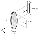
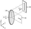
以下では、図面を参照しながら、化学気相法で析出させて育成された多結晶シリコン棒からのX線回折測定用の板状試料の採取例、板状試料からのX線回折プロファイルをθ-2θ法で求める際の測定系例の概略、板状試料からのX線回折プロファイルをφスキャン法で求める際の測定系例の概略、φスキャン測定をミラー指数面<111>、<220>、<311>、<400>について行って得られたチャートの例について説明した上で、板状試料のミラー指数面<111>および<220>についてのφスキャン・チャートに現れるピークの例について説明する。
図1A及び図1Bは、シーメンス法などの化学気相法で析出させて育成された多結晶シリコン棒10からの、X線回折プロファイル測定用の板状試料20の採取例について説明するための図である。図中、符号1で示したものは、表面に多結晶シリコンを析出させてシリコン棒とするためのシリコン芯線である。
なお、この例では、多結晶シリコン棒10の結晶配向度(局所配向ドメインの存在の程度)の径方向依存性の有無を確認すべく3つの部位(CTR:シリコン芯線1に近い部位、EDG:多結晶シリコン棒10の側面に近い部位、R/2:CTRとEGDの中間の部位)から板状試料20を採取しているが、このような部位からの採取に限定されるものではない。
図1Aで例示した多結晶シリコン棒10の直径は概ね120mmであり、この多結晶シリコン棒10の側面側から、直径が概ね20mmで長さが概ね60mmのロッド11を、シリコン芯線1の長手方向と垂直にくり抜く。
そして、図1Bに図示したように、このロッド11のシリコン芯線1に近い部位(CTR)、多結晶シリコン棒10の側面に近い部位(EDG)、CTRとEGDの中間の部位(R/2)からそれぞれ、多結晶シリコン棒10の径方向に垂直な断面を主面とする厚みが概ね2mmの円板状試料(20CTR、20EDG、20R/2)を採取する。
なお、ロッド11を採取する部位、長さ、および本数は、シリコン棒10の直径やくり抜くロッド11の直径に応じて適宜定めればよく、円板状試料20も、くり抜いたロッド11のどの部位から採取してもよいが、シリコン棒10全体の性状を合理的に推定可能な位置であることが好ましい。
例えば、2枚の円板状試料を取得する場合には、シリコン棒の周の半径に対し、中心から半径の2分の1である点よりも中心側にある位置と、外側にある位置の2箇所から円板状試料を取得することが好ましい。更に、例えば比較を行う2つのサンプルの取得位置を、中心から半径の3分の1である点よりも中心側にある位置と、中心から半径の3分の2である点よりも外側にある位置とした場合、より高精度な比較ができる。また、比較する円板状試料は1枚以上であればよく、特に上限はない。
また、円板状試料20の直径を概ね20mmとしたのも例示に過ぎず、直径はX線回折測定時に支障がない範囲で適当に定めればよい。
本発明では、多結晶シリコンの局所配向ドメインをX線回折法により評価するにあたり、上述のようにして採取した板状試料20を、ミラー指数面<hkl>からのブラッグ反射が検出される位置に配置し、スリットにより定められるX線照射領域が板状試料20の主面上をφスキャンするように該板状試料20の中心を回転中心として回転角度φで面内回転させ、上記ミラー指数面からのブラッグ反射強度の板状試料20の回転角度(φ)依存性を示すチャートを求め、該チャートからピークトップの回折強度値とベースラインの回折強度値を求める。そして、このピークトップの回折強度値(P)をベースラインの回折強度値(B)で除した値(回折強度比:P/B=R)を多結晶シリコン中に含まれる局所配向ドメインの評価指標として用いる。
ここで、上述したように、本発明者らの検討によれば、ミラー指数面<111>および<220>からのピークは、局所配向ドメインの評価に特に有効であるから、上記ミラー指数面<hkl>としては、<111>および<220>の少なくとも一方の面であることが好ましい。
また、本発明では、単結晶シリコン製造用原料として用いる多結晶シリコン棒をX線回折法により選択するにあたり、上述の多結晶シリコンの局所配向ドメインの評価方法を利用する。
すなわち、本発明に係る多結晶シリコン棒の選択方法は、単結晶シリコン製造用原料として用いる多結晶シリコン棒をX線回折法により選択するための方法であって、前記多結晶シリコン棒は化学気相法による析出により育成されたものであり、該多結晶シリコン棒の径方向に垂直な断面を主面とする板状試料を採取し、該板状試料をミラー指数面<hkl>からのブラッグ反射が検出される位置に配置し、スリットにより定められるX線照射領域が前記板状試料の主面上をφスキャンするように該板状試料の中心を回転中心として回転角度φで面内回転させ、前記ミラー指数面からのブラッグ反射強度の前記板状試料の回転角度(φ)依存性を示すチャートを求め、該チャートからピークトップの回折強度値とベースラインの回折強度値を求め、前記ピークトップの回折強度値(P)を前記ベースラインの回折強度値(B)で除した値(回折強度比:P/B=R)を判定基準として単結晶シリコン製造用原料としての適否を判断する。
ここでも、上記ミラー指数面<hkl>としては、<111>および<220>の少なくとも一方の面であることが好ましい。
板状試料のミラー指数面<hkl>についてのφスキャン・チャートに現れるピークをどのように定義付けるか等については、ミラー指数面<111>および<220>についてのφスキャン・チャートを例に、後述する。
図2は、円板状試料20からのX線回折プロファイルを、いわゆるθ-2θ法で求める際の測定系例の概略を説明するための図である。スリット30から射出されてコリメートされたX線ビーム40(Cu-Kα線:波長1.54Å)は円板状試料20に入射し、円板状試料20をXY平面内で回転させながら、試料回転角度(θ)毎の回折X線ビームの強度を検知器(不図示)で検出して、θ-2θのX線回折チャートを得る。
図3は、上記で得られたθ-2θのX線回折チャートの例で、ミラー指数面<111>、<220>、<311>、<400>からの強いブラッグ反射がそれぞれ、2θ=28.40°、47.24°、55.98°、68.98°の位置にピークとなって現れる。
図4は、円板状試料20からのX線回折プロファイルを、いわゆるφスキャン法で求める際の測定系の概略を説明するための図である。例えば、円板状試料20の上記θを、ミラー指数面<111>からのブラッグ反射が検出される角度とし、この状態で、円板状試料20の中心から周端に渡る領域にスリットにより定められる細い矩形の領域にX線を照射させ、このX線照射領域が円板状試料20の全面をスキャンするように円板状試料20の中心を回転中心としてYZ面内で回転(φ=0°~360°)させる。
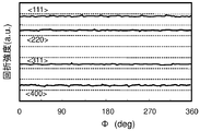
図5は、上記φスキャン測定を、ミラー指数面<111>、<220>、<311>、<400>について行って得られたチャートの一例である。この例では、上記何れのミラー指数面に着目してもブラッグ反射強度は略一定であり、ブラッグ反射強度は回転角φに依存せず、粉末試料と同様のチャートとなっている。つまり、この円板状試料20には、局所配向ドメインが存在しないと判断することができる。
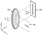
図6は、円板状試料20からのX線回折プロファイルをφスキャン法で求める際の他の測定系例の概略を説明するための図で、この図に示した例では、円板状試料20の両周端に渡る領域にスリットにより定められる細い矩形の領域にX線を照射させ、このX線照射領域が円板状試料20の全面をスキャンするように円板状試料20の中心を回転中心としてYZ面内で回転(φ=0°~180°)させる。
図7は、上記φスキャン測定を、ミラー指数面<111>、<220>、<311>、<400>について行って得られたチャートの一例で、実質的に、図5に示したものと同じφスキャン・チャートが得られている。
図8は、円板状試料20からのX線回折プロファイルをφスキャン法で求める際のもうひとつの測定系例の概略を説明するための図で、この図に示した例では、円板状試料20の主面の全体ではなく、内周領域のみにX線を照射させ、このX線照射領域が円板状試料20の全面をスキャンするように円板状試料20の中心を回転中心としてYZ面内で回転(φ=0°~180°)させる。
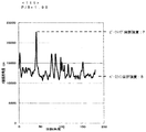
図9Aおよび図9Bは、それぞれ、多結晶シリコン棒の中心部から採取した板状試料のミラー指数面<111>についてのφスキャン・チャート例、および、多結晶シリコン棒の外周部から採取した板状試料のミラー指数面<220>についてのφスキャン・チャート例である。
図9Aのミラー指数面<111>についてのφスキャン・チャートには、多数のピークが表れており、<111>方向に局所的に配向したドメインが存在していることを示している。この例では、最も強いピークのトップの回折強度値(P)と、ベースラインの回折強度値(B)の比(P/B=R)は、1.90と求められる。
また、図9Bのミラー指数面<220>についてのφスキャン・チャートにも、複数のピークが表れており、<220>方向に局所的に配向したドメインが存在していることを示している。この例では、最も強いピークのトップの回折強度値(P)と、ベースラインの回折強度値(B)の比(P/B=R)は、11.2と求められる。
図10は、板状試料のミラー指数面<hkl>についてのφスキャン・チャートに現れるピークをどのように定義付けるかを説明するための図である。
結晶が完全にランダムに配向していれば、特定のミラー指数面<hkl>からの回折強度は一定であるから、φスキャンを行っても「ベースライン」の回折強度は概ね一定のはずである。しかし、局所配向ドメインが存在するとピークが現れ、「ベースライン」も「ノイズ」を帯びたものとなる。
本発明者は、このようなφスキャン・チャート中のピークの有無を、例えば、「ピーク」近傍の「ベースライン」の上限値BHと下限値BLの回折強度値の平均値をベースラインの回折強度値Bとし、「ピーク」のトップの回折強度値Pが、下記の関係式を満足する場合に、当該「ピーク」を局所配向ドメイン評価のためのピークとして採用することとした。
[ΔB/2]×1.5+B<P
後述するように、このような方法において、ミラー指数面<hkl>が<111>である場合の回折強度比(R111)と、ミラー指数面<hkl>が<220>である場合の回折強度比(R220)を求め、回折強度比R111が1.8以下で、かつ、回折強度比R220が12以下である場合に、単結晶シリコン製造用原料として用いる多結晶シリコン棒として選択することが好ましい。
なお、図8に示したようなX線照射領域から得られるφスキャン・チャートと、上述の円板状試料20の主面全体から得られるφスキャン・チャートとの差分を求める等の処理を行うと、円板状試料20の面内での局所配向ドメインの分布を得ることも可能となる。
尤も、図1A~1Bに示したような態様で採取された円板状試料20については面内での局所配向ドメイン分布は生じないと考えられるが、本発明に係る局所配向ドメインの評価は、シーメンス法等により育成された多結晶シリコン棒の選択方法としてのみならず、多結晶シリコン全般をX線回折法により評価する方法としても有意であることは言うまでもない。
従って、例えば、化学気相法による析出で育成された多結晶シリコン棒の径方向と平行に切り出された円板状試料につき面内での局所配向ドメイン分布を求めることにより、多結晶シリコン棒内での局所配向ドメインの有無乃至多結晶シリコン棒の口径拡大に伴う局所配向ドメインの変化等を知ることも可能となり、これにより単結晶シリコン製造用原料として好適な多結晶シリコン棒を選択することが可能となる。
つまり、局所配向ドメインの存在が認められない領域からのミラー指数面<hkl>についてのφスキャン・チャートにはピークが現れない一方、局所配向ドメインの存在が認められる領域からのミラー指数面<hkl>についてのφスキャン・チャートにはピークが現れる。本発明者らの検討によれば、この現象は、ミラー指数面<hkl>が、<111>と<220>において特に顕著である。
従って、上述の手法で多結晶シリコン中の局所配向ドメインの存否を評価し、その程度に応じて、単結晶シリコン製造用原料として好適な多結晶シリコン棒乃至は当該多結晶シリコン棒を破砕して得られた多結晶シリコン塊を選択することにより、単結晶シリコン製造の安定性が高まることになる。
ここで、各ミラー指数面<hkl>についてのφスキャン・チャートに現れるピークの最大値は、上述の意味での「局所配向ドメイン」を構成する領域にある結晶粒の配向の程度に依存しており、ピークの幅は、「局所配向ドメイン」にX線が照射されるφスキャン時の試料の回転角度、つまり、「局所配向ドメイン」の領域の幅に相当するものであり、「局所配向ドメイン」の形状が円形であれば直径に相当し、不定形であればこれを円形近似した場合の直径に相当する。
本発明者らの検討により、光学顕微鏡観察において「局所配向ドメイン」が確認されない試料であっても、上述の手法で評価するとφスキャン・チャートにピークが現れ、「局所配向ドメイン」を含むと判断されるものがあることが明らかになった。つまり、本発明の方法によれば、光学顕微鏡では観察不能乃至は見落される程度の「局所配向ドメイン」であっても、検出が可能である。
また、本発明者らの検討によれば、多数の多結晶シリコン棒から試料を採取して上述の局所配向ドメイン評価を行い、各多結晶シリコン棒を原料としてFZ法で単結晶化を試みたところ、局所配向ドメインの含有レベルが低いと評価されるものでは単結晶化の工程で結晶線が消失しない一方、局所配向ドメインの含有レベルが比較的高いと評価されるものでは単結晶化の工程で結晶線が消失する確率が高いことが判明した。
本発明では、局所配向ドメインの含有レベルが低いと判断する基準として、ミラー指数面<hkl>が<111>である場合の回折強度比(R111)と、ミラー指数面<hkl>が<220>である場合の回折強度比(R220)を求め、回折強度比R111が1.8以下で、かつ、回折強度比R220が12以下であることを提案する。
このような局所配向ドメインの生成メカニズムの詳細は不明な点も多いが、多結晶シリコン棒を製造する際には、その成長に伴って表面積当たりの原料供給量や表面温度の状態も変化するため、局所配向ドメインは、シリコン棒の長軸方向での部位依存性よりも、半径方向での部位依存性の方が高くなりやすい傾向がある。
異なる析出条件下で育成された多結晶シリコン棒を6本準備した(A~F)。これらの多結晶シリコン棒のそれぞれにつき、図1Aおよび1Bで示した3つの部位から、厚みが概ね2mmの円板状試料(20CTR、20EDG、20R/2)を採取し、図6に示した測定系により、ミラー指数面<111>及び<220>のφスキャン・チャートを得た。なお、円板状試料20の直径は約20mmである。
これらの多結晶シリコン棒から得られた円板状試料毎(A~F)のピークトップの回折強度とベースラインの回折強度Bの比(P/B)、および、これらの多結晶シリコン棒を用いてFZ法による単結晶シリコンロッドの育成を行った際の結晶線消失の有無を、表1に纏めた。なお、何れの多結晶シリコン棒についても、同一成長方向の中央部と外側部から取得した円板状試料を評価して得た値のうちの高い方で評価しており、回折強度の単位はkcpsである。

A~Fの何れの試料についても、光学顕微鏡観察において、局所配向ドメインは確認されなかったが、試料DとEにおいて、FZ結晶線の消失が確認された。
試料DにおいてFZ結晶線の消失が確認された理由は、<220>のP/Bの値が12を超えたためであると考えられる。また、試料EにおいてFZ結晶線の消失が確認された理由は、<110>のP/Bの値が1.8を超えたためであると考えられる。
そこで、本発明では、局所配向ドメインの含有レベルが低いと判断する基準として、ミラー指数面<hkl>が<111>である場合の回折強度比(R111)と、ミラー指数面<hkl>が<220>である場合の回折強度比(R220)を求め、回折強度比R111が1.8以下で、かつ、回折強度比R220が12以下であることを提案する。
このように、本発明によれば、光学顕微鏡では観察不能乃至は見落される程度の「局所配向ドメイン」であってもその検出が可能であり、これを利用することで、単結晶シリコン製造用原料として好適な多結晶シリコンを高い定量性と再現性で選別し、単結晶シリコンの安定的製造に寄与する技術の提供が可能となる。
1 シリコン芯線
10 多結晶シリコン棒
11 ロッド
20 板状試料
30 スリット
40 X線ビーム
10 多結晶シリコン棒
11 ロッド
20 板状試料
30 スリット
40 X線ビーム
Claims (10)
- 多結晶シリコン中に含まれる局所配向ドメインをX線回折法により評価する方法であって、
前記多結晶シリコンを板状試料とし、該板状試料をミラー指数面<hkl>からのブラッグ反射が検出される位置に配置し、スリットにより定められるX線照射領域が前記板状試料の主面上をφスキャンするように該板状試料の中心を回転中心として回転角度φで面内回転させ、前記ミラー指数面からのブラッグ反射強度の前記板状試料の回転角度(φ)依存性を示すチャートを求め、該チャートからピークトップの回折強度値とベースラインの回折強度値を求め、前記ピークトップの回折強度値(P)を前記ベースラインの回折強度値(B)で除した値(回折強度比:P/B=R)を前記多結晶シリコン中に含まれる局所配向ドメインの評価指標として用いる、ことを特徴とする多結晶シリコン中の局所配向ドメインの評価方法。 - 前記ミラー指数面<hkl>は、<111>および<220>の少なくとも一方の面である、請求項1に記載の多結晶シリコン中の局所配向ドメインの評価方法。
- 単結晶シリコン製造用原料として用いる多結晶シリコン棒をX線回折法により選択するための方法であって、
前記多結晶シリコン棒は化学気相法による析出により育成されたものであり、該多結晶シリコン棒の径方向に垂直な断面を主面とする板状試料を採取し、該板状試料をミラー指数面<hkl>からのブラッグ反射が検出される位置に配置し、スリットにより定められるX線照射領域が前記板状試料の主面上をφスキャンするように該板状試料の中心を回転中心として回転角度φで面内回転させ、前記ミラー指数面からのブラッグ反射強度の前記板状試料の回転角度(φ)依存性を示すチャートを求め、該チャートからピークトップの回折強度値とベースラインの回折強度値を求め、前記ピークトップの回折強度値(P)を前記ベースラインの回折強度値(B)で除した値(回折強度比:P/B=R)を判定基準として単結晶シリコン製造用原料としての適否を判断する、ことを特徴とする多結晶シリコン棒の選択方法。 - 前記ミラー指数面<hkl>は、<111>および<220>の少なくとも一方の面である、請求項3に記載の多結晶シリコン棒の選択方法。
- 前記ミラー指数面<hkl>が<111>である場合の回折強度比(R111)と、前記ミラー指数面<hkl>が<220>である場合の回折強度比(R220)を求め、前記回折強度比R111が1.8以下で、かつ、前記回折強度比R220が12以下である場合に、単結晶シリコン製造用原料として用いる多結晶シリコン棒として選択する、請求項4に記載の多結晶シリコン棒の選択方法。
- 前記多結晶シリコン棒はシーメンス法で育成されたものである、請求項3乃至5の何れか1項に記載の多結晶シリコン棒の選択方法。
- 請求項3乃至5の方法により選択された多結晶シリコン棒。
- 請求項7に記載の多結晶シリコン棒を破砕して得られた多結晶シリコン塊。
- 請求項7に記載の多結晶シリコン棒をシリコン原料として用いる単結晶シリコンの製造方法。
- 請求項8に記載の多結晶シリコン塊を原料として用いる単結晶シリコンの製造方法。
Applications Claiming Priority (2)
| Application Number | Priority Date | Filing Date | Title |
|---|---|---|---|
| JP2013-111864 | 2013-05-28 | ||
| JP2013111864A JP5984741B2 (ja) | 2013-05-28 | 2013-05-28 | 多結晶シリコン棒の選択方法、および、fz単結晶シリコンの製造方法 |
Publications (1)
| Publication Number | Publication Date |
|---|---|
| WO2014192245A1 true WO2014192245A1 (ja) | 2014-12-04 |
Family
ID=51988298
Family Applications (1)
| Application Number | Title | Priority Date | Filing Date |
|---|---|---|---|
| PCT/JP2014/002609 Ceased WO2014192245A1 (ja) | 2013-05-28 | 2014-05-19 | 多結晶シリコン中の局所配向ドメインの評価方法 |
Country Status (2)
| Country | Link |
|---|---|
| JP (1) | JP5984741B2 (ja) |
| WO (1) | WO2014192245A1 (ja) |
Cited By (1)
| Publication number | Priority date | Publication date | Assignee | Title |
|---|---|---|---|---|
| CN107389709A (zh) * | 2017-06-29 | 2017-11-24 | 中国建筑材料科学研究总院 | 基于xrd优选硅质物料的方法及其应用 |
Citations (2)
| Publication number | Priority date | Publication date | Assignee | Title |
|---|---|---|---|---|
| JP2008039437A (ja) * | 2006-08-01 | 2008-02-21 | Rigaku Corp | X線回折装置 |
| WO2012164803A1 (ja) * | 2011-06-02 | 2012-12-06 | 信越化学工業株式会社 | 多結晶シリコン棒の選択方法および単結晶シリコンの製造方法 |
Family Cites Families (4)
| Publication number | Priority date | Publication date | Assignee | Title |
|---|---|---|---|---|
| JP5012386B2 (ja) * | 2007-10-04 | 2012-08-29 | 三菱マテリアル株式会社 | 多結晶シリコンロッドの製造方法 |
| CN102300808B (zh) * | 2009-02-27 | 2013-08-21 | 株式会社德山 | 多晶硅棒及其制造装置 |
| US8399072B2 (en) * | 2009-04-24 | 2013-03-19 | Savi Research, Inc. | Process for improved chemcial vapor deposition of polysilicon |
| JP5689382B2 (ja) * | 2011-07-25 | 2015-03-25 | 信越化学工業株式会社 | 多結晶シリコンロッドの破砕方法 |
-
2013
- 2013-05-28 JP JP2013111864A patent/JP5984741B2/ja active Active
-
2014
- 2014-05-19 WO PCT/JP2014/002609 patent/WO2014192245A1/ja not_active Ceased
Patent Citations (2)
| Publication number | Priority date | Publication date | Assignee | Title |
|---|---|---|---|---|
| JP2008039437A (ja) * | 2006-08-01 | 2008-02-21 | Rigaku Corp | X線回折装置 |
| WO2012164803A1 (ja) * | 2011-06-02 | 2012-12-06 | 信越化学工業株式会社 | 多結晶シリコン棒の選択方法および単結晶シリコンの製造方法 |
Non-Patent Citations (1)
| Title |
|---|
| HIDEKI TSUYA ET AL.: "Advancing Si single crystals into the I-G bit era", OYO BUTSURI, vol. 60, no. 8, 10 August 1991 (1991-08-10), pages 752 - 765 * |
Cited By (2)
| Publication number | Priority date | Publication date | Assignee | Title |
|---|---|---|---|---|
| CN107389709A (zh) * | 2017-06-29 | 2017-11-24 | 中国建筑材料科学研究总院 | 基于xrd优选硅质物料的方法及其应用 |
| CN107389709B (zh) * | 2017-06-29 | 2019-06-25 | 中国建筑材料科学研究总院 | 基于xrd优选硅质物料的方法及其应用 |
Also Published As
| Publication number | Publication date |
|---|---|
| JP2014231440A (ja) | 2014-12-11 |
| JP5984741B2 (ja) | 2016-09-06 |
Similar Documents
| Publication | Publication Date | Title |
|---|---|---|
| JP5828795B2 (ja) | 多結晶シリコンの結晶配向度評価方法、多結晶シリコン棒の選択方法、および単結晶シリコンの製造方法 | |
| CN104395740B (zh) | 多晶硅的晶体取向度评价方法、多晶硅棒的选择方法、多晶硅棒、多晶硅块以及单晶硅的制造方法 | |
| JP5947248B2 (ja) | 多結晶シリコン棒の選択方法 | |
| CN103547713B (zh) | 多晶硅棒的选择方法及单晶硅的制造方法 | |
| CN107250038B (zh) | 多晶硅棒及其制造方法和fz硅单晶 | |
| JP5969956B2 (ja) | 多結晶シリコンの粒径評価方法および多結晶シリコン棒の選択方法 | |
| JP5923463B2 (ja) | 多結晶シリコンの結晶粒径分布の評価方法、多結晶シリコン棒の選択方法、多結晶シリコン棒、多結晶シリコン塊、および、単結晶シリコンの製造方法 | |
| JP5984741B2 (ja) | 多結晶シリコン棒の選択方法、および、fz単結晶シリコンの製造方法 | |
| KR102284506B1 (ko) | 다결정 실리콘, fz 단결정 실리콘, 및 그의 제조 방법 | |
| JP2019019010A (ja) | 多結晶シリコン棒および多結晶シリコン棒の製造方法 |
Legal Events
| Date | Code | Title | Description |
|---|---|---|---|
| 121 | Ep: the epo has been informed by wipo that ep was designated in this application |
Ref document number: 14803489 Country of ref document: EP Kind code of ref document: A1 |
|
| NENP | Non-entry into the national phase |
Ref country code: DE |
|
| 122 | Ep: pct application non-entry in european phase |
Ref document number: 14803489 Country of ref document: EP Kind code of ref document: A1 |