WO2014185233A1 - 静電容量センサ - Google Patents
静電容量センサ Download PDFInfo
- Publication number
- WO2014185233A1 WO2014185233A1 PCT/JP2014/061397 JP2014061397W WO2014185233A1 WO 2014185233 A1 WO2014185233 A1 WO 2014185233A1 JP 2014061397 W JP2014061397 W JP 2014061397W WO 2014185233 A1 WO2014185233 A1 WO 2014185233A1
- Authority
- WO
- WIPO (PCT)
- Prior art keywords
- frequency
- oscillator
- capacitance
- comparator
- capacitance sensor
- Prior art date
- Legal status (The legal status is an assumption and is not a legal conclusion. Google has not performed a legal analysis and makes no representation as to the accuracy of the status listed.)
- Ceased
Links
Images



Classifications
-
- H—ELECTRICITY
- H03—ELECTRONIC CIRCUITRY
- H03K—PULSE TECHNIQUE
- H03K17/00—Electronic switching or gating, i.e. not by contact-making and –breaking
- H03K17/94—Electronic switching or gating, i.e. not by contact-making and –breaking characterised by the way in which the control signals are generated
- H03K17/945—Proximity switches
- H03K17/955—Proximity switches using a capacitive detector
-
- H—ELECTRICITY
- H03—ELECTRONIC CIRCUITRY
- H03K—PULSE TECHNIQUE
- H03K2217/00—Indexing scheme related to electronic switching or gating, i.e. not by contact-making or -breaking covered by H03K17/00
- H03K2217/94—Indexing scheme related to electronic switching or gating, i.e. not by contact-making or -breaking covered by H03K17/00 characterised by the way in which the control signal is generated
- H03K2217/96—Touch switches
- H03K2217/9607—Capacitive touch switches
- H03K2217/96071—Capacitive touch switches characterised by the detection principle
- H03K2217/960715—Rc-timing; e.g. measurement of variation of charge time or discharge time of the sensor
-
- H—ELECTRICITY
- H03—ELECTRONIC CIRCUITRY
- H03K—PULSE TECHNIQUE
- H03K2217/00—Indexing scheme related to electronic switching or gating, i.e. not by contact-making or -breaking covered by H03K17/00
- H03K2217/94—Indexing scheme related to electronic switching or gating, i.e. not by contact-making or -breaking covered by H03K17/00 characterised by the way in which the control signal is generated
- H03K2217/96—Touch switches
- H03K2217/9607—Capacitive touch switches
- H03K2217/960735—Capacitive touch switches characterised by circuit details
- H03K2217/96074—Switched capacitor
-
- H—ELECTRICITY
- H03—ELECTRONIC CIRCUITRY
- H03K—PULSE TECHNIQUE
- H03K2217/00—Indexing scheme related to electronic switching or gating, i.e. not by contact-making or -breaking covered by H03K17/00
- H03K2217/94—Indexing scheme related to electronic switching or gating, i.e. not by contact-making or -breaking covered by H03K17/00 characterised by the way in which the control signal is generated
- H03K2217/96—Touch switches
- H03K2217/9607—Capacitive touch switches
- H03K2217/960755—Constructional details of capacitive touch and proximity switches
- H03K2217/960765—Details of shielding arrangements
Definitions
- the present invention relates to a capacitance of a detection electrode or a capacitance sensor that detects a change thereof, and more particularly to a capacitance sensor using an oscillator.
- Patent Document 1 discloses a fluid that uses the above-described capacitive proximity sensor.
- a fluid detection sensor for detecting presence / absence, configuration, state change, and the like is disclosed.
- the capacitive proximity sensor includes an oscillation circuit as a circuit for detecting the change in capacitance, and a part of the oscillation circuit serves as a detection electrode.
- the capacitance C X of the detection electrode increases and the oscillation frequency f OSC changes.
- the capacitive proximity sensor includes a determination circuit that determines whether or not the oscillation frequency f OSC of the oscillation circuit has reached a predetermined reference value, and the proximity of the object is determined based on the determination result. Can be detected.
- FIG. 5 is a circuit diagram showing a schematic configuration of the capacitive proximity sensor.
- the capacitive proximity sensor 101 includes an oscillation circuit 111 and a determination circuit 112.
- the oscillation circuit 111 is a Wien bridge oscillation circuit including a detection electrode 113, an operational amplifier A, a capacitance element C 2 , and resistance elements R 1 to R 4 .
- the sign of the resistive element is also the resistance value of the resistive element
- the sign of the capacitive element is also the capacitance of the capacitive element.
- the oscillation circuit 111 outputs a signal having an oscillation frequency f OSC that satisfies the above formula (1) to the determination circuit 112.
- the determination circuit 112 monitors a change in the oscillation frequency f OSC of the signal from the oscillation circuit 111, converts it into a required signal according to the purpose, and outputs it.
- the determination circuit 112 includes a period / voltage conversion circuit that converts the oscillation frequency f OSC into a DC voltage, a comparator that compares the converted DC voltage with a predetermined reference value, and the DC voltage that is larger or smaller than the reference value. And an output circuit for issuing a predetermined alarm and a control signal.
- Japanese Patent Publication Japanese Patent Laid-Open No. 11-230815 (published Aug. 27, 1999)”
- the oscillation frequency f OSC of the oscillation circuit 111 and the reference value of the determination circuit 112 have large manufacturing variations or change due to deterioration over time. For this reason, it is difficult to accurately detect a change in capacitance in the detection electrode 113 unless calibration at the time of manufacture and correction at power-on are performed.
- the present invention has been made in view of the above problems, and its purpose is to accurately detect the capacitance of the detection electrode or its change without performing calibration at the time of manufacture and correction at the time of power-on.
- An object of the present invention is to provide a capacitive sensor that can detect.
- a capacitance sensor is a capacitance sensor that detects a capacitance of a detection electrode or a change thereof, and includes the detection electrode in order to solve the above-described problem.
- An oscillator that oscillates at an oscillation frequency based on the product of the above, and a comparator that compares the oscillation frequency of the oscillator with a reference frequency and outputs a signal corresponding to the capacitance.
- a clock generator for providing a reference frequency of the comparator and a switching frequency of the switched capacitor.
- the reference frequency and the switching frequency are provided from a common clock generator, manufacturing variations and changes due to aging in the clock generator affect the reference frequency of the comparator. Does not affect the comparison result of the comparator, so that it is possible to accurately detect the capacitance of the detection electrode or its change without performing calibration at the time of manufacture and correction at power-on. There is an effect.
- FIG. 1 is a circuit diagram showing a schematic configuration of a capacitance sensor according to a first embodiment of the present invention. It is a graph which shows the time change of the output signal of an oscillator and a comparator in the above-mentioned capacitance sensor. It is a circuit diagram which shows schematic structure of the electrostatic capacitance sensor which concerns on 2nd Embodiment of this invention. It is a circuit diagram which shows schematic structure of the electrostatic capacitance sensor which concerns on 3rd Embodiment of this invention. It is a circuit diagram which shows schematic structure of the conventional electrostatic capacitance type proximity sensor.
- FIGS. 1 to 4 Embodiments of the present invention will be described with reference to FIGS. 1 to 4 as follows.
- members having the same functions as those shown in the embodiments are denoted by the same reference numerals, and description thereof is omitted as appropriate.
- FIG. 1 is a circuit diagram showing a schematic configuration of the capacitance sensor according to the first embodiment of the present invention.
- the capacitance sensor 1 detects the capacitance C X of the detection electrode 2, and is used for, for example, a water level sensor, a touch sensor, a proximity sensor, and the like.
- the capacitance sensor 1 includes an oscillator 11, a comparator 12, a clock generator 13, and a frequency divider 14.
- the oscillator 11 outputs a signal having an oscillation frequency f OSC to the comparator 12.
- the comparator 12 compares the oscillation frequency f OSC of the signal from the oscillator 11 with the reference frequency f ref, and outputs a signal corresponding to the capacitance C X to an external device (not shown).
- the oscillator 11 includes a switched capacitor 21 instead of the resistance element.
- Equivalent resistance R of the switched capacitor 21 uses a capacitor C R and the switching frequency f SW of the switched capacitor 21 is expressed by the following equation.
- R 1 / (f SW ⁇ C R ) (3). Therefore, the oscillation frequency f OSC of the oscillator 11 is expressed by the following equation using the above equations (2) and (3).
- f OSC (f SW / 2 ⁇ ) ⁇ (C R / C X ) (4).
- the clock generator 13 generates a clock signal having the clock frequency f CLK and outputs it to the frequency divider 14 and the comparator 12.
- the frequency divider 14 divides the clock signal from the clock generator 13 by the frequency division ratio M, and supplies the frequency- divided clock signal of the frequency f CLK / M to the switched capacitor 21 of the oscillator 11.
- the switched capacitor 21 performs switching based on the clock signal.
- f SW f CLK / M. Therefore, the oscillation frequency f OSC of the oscillator 11 is expressed by the following equation from the above equation (4).
- f OSC (1 / 2 ⁇ ) ⁇ (f CLK / M) ⁇ ( CR / C X ) (5).
- the comparator 12 sets the frequency f CLK of the clock signal from the clock generator 13 as the reference frequency f ref .
- the oscillation frequency f OSC of the oscillator 11 and the reference frequency f ref of the comparator 12 depend on the frequency f CLK of the clock signal of the common clock generator 13, the oscillation frequency f OSC and the reference frequency f ref The accuracy of the clock signal from the clock generator 13 does not depend on the comparison result.
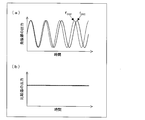
- FIG. 2A and 2B are graphs showing temporal changes in the output signals of the oscillator 11 and the comparator 12 in the electrostatic capacitance sensor 1, respectively.
- a solid line indicates a case where the clock generator 13 generates a clock signal having the frequency f CLK
- a broken line indicates a frequency at which the clock generator 13 is different from the frequency f CLK due to manufacturing variation, aging deterioration, and the like.
- the case where a clock signal of f ′ CLK is generated is shown.
- the oscillation frequency f OSC of the oscillator 11 depends on the frequency f CLK of the clock generator 13. Therefore, the frequency of the clock generator 13, changes from f CLK to f'CLK, the oscillation frequency of the oscillator 11, as shown in FIG. 2 (a), changes from f OSC to f'OSC.
- the comparator 12 as a result of comparison between the oscillation frequency f OSC and the reference frequency f ref, determined frequency ratio (f ref / f OSC), the frequency ratio signal indicating the (f ref / f OSC), static Assume that the signal corresponding to the capacitance C X is output to the external device.
- the frequency ratio (f ref / f OSC ) is expressed by the following equation and does not depend on the frequency f CLK of the clock signal.
- FIG. 3 is a circuit diagram showing a schematic configuration of the capacitance sensor according to the second embodiment of the present invention.
- the capacitive sensor 1 according to the present embodiment is different from the capacitive sensor 1 according to the first embodiment in that the oscillator is a Wien bridge type oscillator 31 including the detection electrode 2, and the other configurations are the same. It is.
- the Wien bridge oscillator 31 has a configuration including a band-pass filter and a non-inverting amplifier circuit. Since the detailed configuration of the Wien bridge type oscillator 31 is known, its description is omitted.
- the resistance in the bandpass filter is realized by the switched capacitors 32 and 33. Further, the switched capacitors 32 and 33 perform switching based on the clock signal from the frequency divider 14 in the same manner as the switched capacitor 21 shown in FIG. Accordingly, the equivalent resistance R 1 of the switched capacitor 32 is M / (f CLK ⁇ C R1 ) using the capacitance C R1 of the switched capacitor 32, and the equivalent resistance R 2 of the switched capacitor 33 is the capacitance C of the switched capacitor 33. Using R2 , M / (f CLK ⁇ C R2 ).
- f ref / f WIEN The frequency ratio (f ref / f WIEN ) between the oscillation frequency f WIEN and the reference frequency f ref in the comparator 12 is expressed by the following equation.
- the oscillation frequency f WIEN and the frequency ratio (f ref / f WIEN ) are based on the capacity ratios (C 1 / C R1 ), (C 2 / C R2 ), and (C X / C R1 ). .
- the capacity ratio indicating the relative relationship between a plurality of capacities has small manufacturing variations and small changes due to aging, so that the accuracy is good and the error is about ⁇ 1%. Therefore, the capacity ratios (C 1 / C R1 ) and (C 2 / C R2 ) have good accuracy.
- the capacity ratio (C X / C R1 ) is (C X / C R1 ) ⁇ 1/2 and (C X / C R1 ) 1/2 in the above formulas (7) and (8). Yes.
- C R1 C R10 (1 + ⁇ ).
- This (C X / C R1 ) ⁇ 1/2 (C X / C R10 ) ⁇ 1/2 ⁇ (1 + ⁇ ) 1/2 ⁇ (C X / C R10 ) ⁇ 1/2 ⁇ (1+ ( ⁇ / 2) ) It becomes.
- the Wien bridge type oscillator has a very low oscillation frequency accuracy.
- the Wien-bridge oscillator 31 of this embodiment improves the accuracy of the oscillation frequency f WIEN by adopting the above configuration.
- the accuracy of the frequency ratio (f ref / f WIEN ) of the comparator 12 is also improved, so that the accuracy of the capacitance sensor 1 is improved. Therefore, it is possible to detect the capacitance C X of the detection electrode 2 or a change thereof more accurately without performing calibration at the time of manufacture and correction at the time of power-on.
- CR oscillators such as the oscillator 11 and the Wien bridge type oscillator 31 generally have an oscillation frequency of several Hz to several hundred KHz, which is lower than the clock frequency f CLK of the clock generator 13. Therefore, the comparator 12 uses a counter circuit or the like to count the period of the signal of the oscillation frequency f WIEN from the Wien bridge type oscillator 31 with the clock signal of the clock frequency f CLK , thereby calculating the frequency ratio (f ref / f WIEN ) may be determined. In this case, the comparator 12 can obtain the frequency ratio (f ref / f WIEN ) with a simple circuit configuration.
- the frequency division ratio M of the frequency divider 14 is large.
- the ratio of the change in the frequency ratio (f ref / f WIEN ) of the comparator 12 to the change in the capacitance C X of the detection electrode 2 increases as shown in the above equation (8), the electrostatic capacitance A change in the capacitance CX can be detected with high accuracy. As a result, the accuracy of the capacitance sensor 1 can be improved.
- the capacitance element C 1 connected in parallel to the detection electrode 2 is provided in the Wien bridge type oscillator 31.
- the capacitance element C 1 may be omitted. Good.
- FIG. 4 is a circuit diagram showing a schematic configuration of a capacitance sensor according to the third embodiment of the present invention.
- the capacitance sensor 1 of the present embodiment is different from the capacitance sensor 1 of the second embodiment in the configuration excluding the detection electrode 2 in the Wien bridge type oscillator 31, the comparator 12, the clock generator 13, and the component.
- the difference is that the peripheral device 14 is formed in an IC (integrated circuit) 3, and other configurations are the same.
- the frequency ratio (f ref / f OSC ) that is the comparison result of the comparator 12 is not affected. Absent. Therefore, since it is not necessary to use a high-accuracy clock generator such as a crystal oscillator as the clock generator 13, it is manufactured by a semiconductor manufacturing process such as an LC tuning oscillator, a ring oscillator, or a relaxation oscillator. A clock generator can be used.
- the clock generator 13 can be incorporated in the IC 3 as in the present embodiment. Thereby, the electrostatic capacitance sensor 1 can be reduced in size.
- the capacitance sensor 1 of the above embodiment since the detection electrode 2 is connected to the input side of the operational amplifier A in the oscillators 11 and 31, the potential of the detection electrode 2 is a sine wave having a small amplitude. Will vibrate. As a result, the intensity of the electromagnetic wave radiated from the detection electrode 2 is small and the band is narrow. Further, in the case of the Wien bridge type oscillator 31, the oscillation frequency f WIEN is determined by the pass band of the bandpass filter, so that the influence of noise from the outside can be suppressed. From the above, the capacitance sensor 1 of the above embodiment has high EMC (Electromagnetic Compatibility) resistance. Therefore, the capacitance sensor 1 of the above-described embodiment is suitable for use in devices that require EMC resistance, such as a water level sensor, a touch sensor, and a proximity sensor.
- EMC Electromagnetic Compatibility
- the capacitance sensor is a capacitance sensor that detects the capacitance of a detection electrode or a change thereof, and includes the detection electrode, and is an oscillation based on a product of the capacitance and the resistance.
- An oscillator that oscillates at a frequency; and a comparator that compares the oscillation frequency of the oscillator with a reference frequency and outputs a signal corresponding to the capacitance.
- the oscillator includes a switched capacitor that realizes the resistor. And a clock generator that provides a reference frequency of the comparator and a switching frequency of the switched capacitor.
- the oscillator is a CR oscillator that oscillates at an oscillation frequency based on the product of capacitance and resistance. Since the oscillation frequency of the CR oscillator is based on the product (C X ⁇ R) of the capacitance C X and the resistance R of the detection electrode, if the resistance R is known, the oscillation frequency can be measured by measuring the oscillation frequency. The capacitance Cx can be estimated.
- the resistor R is realized by a switched capacitor. Equivalent resistance R of the switched capacitor, the switching frequency is f SW, the capacitance and C R, since the formula (3), the oscillation frequency of the oscillator, the switching frequency f SW of the switched capacitor Will depend.
- the comparator compares the oscillation frequency with a reference frequency.
- the manufacturing variation at the reference frequency and the change due to aging are derived from the manufacturing variation at the clock generator that provides the reference frequency and the change due to aging.
- the reference frequency and the switching frequency f SW are provided from a common clock generator.
- manufacturing variations and changes due to aging in the clock generator propagate to the reference frequency and the switching frequency f SW , and further propagate to the oscillation frequency f OSC that depends on the switching frequency f SW.
- the comparator the reference frequency and the oscillation frequency f OSC are compared, so that the manufacturing variation and the change due to aging deterioration do not depend on the comparison result.
- the reference frequency and the switching frequency f SW may be a clock frequency of the clock signal generated by the clock generator, or a signal generated from the clock signal, such as a frequency obtained by dividing the clock frequency. May be the frequency.
- the oscillator is a Wien bridge oscillator.
- the Wien bridge type oscillator has a very low oscillation frequency accuracy.
- an accurate capacitance sensor can be realized even if a Wien bridge type oscillator is used.
- the clock generator Even if the clock generator has a large manufacturing variation or a large change due to aging, the comparison result of the comparator is not affected. Therefore, it is not necessary to use a high-accuracy clock generator such as a crystal oscillator as the clock generator, and the clock generator is manufactured by a semiconductor manufacturing process such as an LC tuned oscillator, ring oscillator, or relaxation oscillator.
- a clock generator can be used.
- the configuration excluding at least the detection electrode in the oscillator, the comparator, and the clock generator are included in one integrated circuit. It may be formed. In this case, the capacitance sensor can be reduced in size.
- the capacitance sensor according to Aspect 4 of the present invention is the counter circuit according to Aspects 1 to 3, wherein the comparator counts the oscillation frequency signal from the oscillator with a clock signal that provides the reference frequency. May be provided.
- the comparator can compare the oscillation frequency and the reference frequency with a simple circuit configuration.
- the capacitive sensor according to aspect 5 of the present invention is the frequency divider according to any one of aspects 1 to 4, wherein the clock signal from the clock generator is divided and the divided clock signal is supplied to the switched capacitor. May be further provided.
- the frequency dividing ratio of the frequency divider is large. As the frequency division ratio increases, the ratio of the reference frequency to the oscillation frequency in the comparator increases with respect to the change in capacitance of the detection electrode, so that the change in capacitance can be accurately detected. Can be detected. As a result, the accuracy of the capacitance sensor can be improved.
- the capacitance sensor according to the present invention is detected without a calibration at the time of manufacture and a correction at the time of power-on by providing a reference frequency and a switching frequency from a common clock generator. Since the capacitance of the electrode or its change can be accurately detected, the present invention can be applied to any capacitance sensor using an oscillator.
Landscapes
- Measurement Of Resistance Or Impedance (AREA)
Abstract
発振器(11)は、抵抗と、検出電極(2)の静電容量との積に基づく発振周波数で発振し、比較器(12)は、発振周波数と基準周波数とを比較する。発振器(11)は、抵抗を実現するスイッチトキャパシタ(21)を備え、クロック生成器(13)は、基準周波数とスイッチング周波数とを提供する。
Description
本発明は、検出電極の静電容量又はその変化を検出する静電容量センサに関し、特に、発振器を用いた静電容量センサに関する。
従来、静電容量の変化を検出することにより物体の接近を検知する静電容量形近接センサが知られており、例えば、特許文献1には、上記静電容量形近接センサを用いて、流体の有無、構成、状態変化などを検知する流体検知センサが開示されている。
上記静電容量形近接センサは、上記静電容量の変化を検出する回路として発振回路を備えており、該発振回路の一部が検出電極となっている。上記発振回路は、上記物体が接近すると、上記検出電極の静電容量CXが増加して、発振周波数fOSCが変化する。そして、上記静電容量形近接センサは、上記発振回路の発振周波数fOSCが所定の基準値に達したか否かを判定する判定回路を備えており、該判定の結果により、上記物体の接近を検知することができる。
図5は、上記静電容量形近接センサの概略構成を示す回路図である。図示のように、静電容量形近接センサ101は、発振回路111及び判定回路112を備えている。図示の例では、発振回路111は、検出電極113と、演算増幅器A、静電容量素子C2、及び抵抗素子R1~R4とを備えたウィーンブリッジ型発振回路である。該ウィーンブリッジ型発振回路の発振周波数fOSCは次式で表される。
fOSC=(2π×(CX×C2×R1×R2)1/2)-1 ・・・(1)。
なお、本願では、抵抗素子の符号は、それぞれ、抵抗素子の抵抗値でもあり、静電容量素子の符号は、静電容量素子の容量でもある。
fOSC=(2π×(CX×C2×R1×R2)1/2)-1 ・・・(1)。
なお、本願では、抵抗素子の符号は、それぞれ、抵抗素子の抵抗値でもあり、静電容量素子の符号は、静電容量素子の容量でもある。
従って、静電容量CXが減少すると、発振周波数fOSCは増加する。発振回路111は、上記式(1)を満たす発振周波数fOSCの信号を判定回路112に出力する。
判定回路112は、発振回路111からの信号の発振周波数fOSCの変化を監視し、目的に応じて所要の信号に変換して出力するものである。例えば、判定回路112は、発振周波数fOSCを直流電圧に変換する周期/電圧変換回路、変換した直流電圧を所定の基準値と比較するコンパレータ、上記直流電圧が上記基準値よりも大きい又は小さい場合に、所定の警報を発したり制御信号を発したりする出力回路、などで構成される。
しかしながら、上記従来の静電容量形近接センサ101では、発振回路111の発振周波数fOSCと、判定回路112の上記基準値とは、製造バラツキが大きかったり、経年劣化により変化したりする。このため、製造時の較正及び電源投入時の補正を行わなければ、検出電極113における静電容量の変化を正確に検出することは困難であった。
本発明は、上記の問題点に鑑みてなされたものであって、その目的は、製造時の較正及び電源投入時の補正を行わなくても、検出電極の静電容量又はその変化を正確に検出でき
る静電容量センサを提供することにある。
る静電容量センサを提供することにある。
本発明に係る静電容量センサは、検出電極の静電容量又はその変化を検出する静電容量センサであって、上記課題を解決するために、前記検出電極を備え、前記静電容量及び抵抗の積に基づく発振周波数で発振する発振器と、前記発振器の発振周波数を基準周波数と比較して、前記静電容量に対応する信号を出力する比較器とを備えており、前記発振器は、前記抵抗を実現するスイッチトキャパシタを備えており、前記比較器の基準周波数と、前記スイッチトキャパシタのスイッチング周波数とを提供するクロック生成器をさらに備えることを特徴としている。
本発明の一態様によれば、基準周波数及びスイッチング周波数が共通のクロック生成器から提供されることにより、該クロック生成器における製造バラツキと経年劣化による変化とは、上記比較器の基準周波数に影響を及ぼしても、上記比較器の比較結果には影響を及ぼさないので、製造時の較正及び電源投入時の補正を行わなくても、検出電極の静電容量又はその変化を正確に検出できるという効果を奏する。
本発明の実施形態について、図1~図4に基づいて説明すれば、以下のとおりである。なお、説明の便宜上、各実施形態に示した部材と同一の機能を有する部材については、同一の符号を付記し、適宜その説明を省略する。
〔実施形態1〕
(静電容量センサの構成)
図1は、本発明の第1実施形態に係る静電容量センサの概略構成を示す回路図である。静電容量センサ1は、検出電極2の静電容量CXを検出するものであり、例えば、水位センサ、タッチセンサ、近接センサなどに利用される。図1に示すように、静電容量センサ1は、発振器11、比較器12、クロック生成器13、及び分周器14を備える。
(静電容量センサの構成)
図1は、本発明の第1実施形態に係る静電容量センサの概略構成を示す回路図である。静電容量センサ1は、検出電極2の静電容量CXを検出するものであり、例えば、水位センサ、タッチセンサ、近接センサなどに利用される。図1に示すように、静電容量センサ1は、発振器11、比較器12、クロック生成器13、及び分周器14を備える。
発振器11は、検出電極2を備えたCR発振器であり、該CR発振器の発振周波数fOSCは、検出電極2の静電容量CXと抵抗素子の抵抗Rとを用いて次式で表される。
fOSC=1/(2π×CX×R) ・・・(2)。
発振器11は、発振周波数fOSCの信号を比較器12に出力する。
fOSC=1/(2π×CX×R) ・・・(2)。
発振器11は、発振周波数fOSCの信号を比較器12に出力する。
比較器12は、発振器11からの信号の発振周波数fOSCを基準周波数frefと比較して、静電容量CXに対応する信号を外部の機器(図示せず)に出力する。
本実施形態では、発振器11は、上記抵抗素子に代えて、スイッチトキャパシタ21を
備えている。スイッチトキャパシタ21の等価抵抗Rは、スイッチトキャパシタ21の容量CR及びスイッチング周波数fSWを用いて、次式で表される。
R=1/(fSW×CR) ・・・(3)。
従って、発振器11の発振周波数fOSCは、上記式(2)・(3)により次式となる。fOSC=(fSW/2π)×(CR/CX) ・・・(4)。
備えている。スイッチトキャパシタ21の等価抵抗Rは、スイッチトキャパシタ21の容量CR及びスイッチング周波数fSWを用いて、次式で表される。
R=1/(fSW×CR) ・・・(3)。
従って、発振器11の発振周波数fOSCは、上記式(2)・(3)により次式となる。fOSC=(fSW/2π)×(CR/CX) ・・・(4)。
クロック生成器13は、クロック周波数fCLKのクロック信号を生成し、分周器14及び比較器12に出力する。
分周器14は、クロック生成器13からのクロック信号を分周比Mで分周し、分周された周波数fCLK/Mのクロック信号を、発振器11のスイッチトキャパシタ21に供給する。スイッチトキャパシタ21は、上記クロック信号に基づいてスイッチングを行う。これにより、fSW=fCLK/Mとなる。従って、発振器11の発振周波数fOSCは、上記式(4)から次式となる。
fOSC=(1/2π)×(fCLK/M)×(CR/CX) ・・・(5)。
fOSC=(1/2π)×(fCLK/M)×(CR/CX) ・・・(5)。
一方、比較器12は、クロック生成器13からのクロック信号の周波数fCLKを基準周波数frefとする。これにより、発振器11の発振周波数fOSCと比較器12の基準周波数frefとは、共通のクロック生成器13のクロック信号の周波数fCLKに依存するので、発振周波数fOSCと基準周波数frefとの比較結果には、クロック生成器13のクロック信号の精度は依存しなくなる。
(静電容量センサの動作)
この点を、図2を参照して具体的に説明する。図2の(a)・(b)は、それぞれ、静電容量センサ1における発振器11及び比較器12の出力信号の時間変化を示すグラフである。同図において、実線は、クロック生成器13が周波数fCLKのクロック信号を生成する場合を示しており、破線は、製造バラツキ、経年劣化などにより、クロック生成器13が周波数fCLKとは異なる周波数f´CLKのクロック信号を生成する場合を示している。
この点を、図2を参照して具体的に説明する。図2の(a)・(b)は、それぞれ、静電容量センサ1における発振器11及び比較器12の出力信号の時間変化を示すグラフである。同図において、実線は、クロック生成器13が周波数fCLKのクロック信号を生成する場合を示しており、破線は、製造バラツキ、経年劣化などにより、クロック生成器13が周波数fCLKとは異なる周波数f´CLKのクロック信号を生成する場合を示している。
上記式(5)のように、発振器11の発振周波数fOSCは、クロック生成器13の周波数fCLKに依存する。従って、クロック生成器13の周波数が、fCLKからf´CLKに変化すると、発振器11の発振周波数は、図2の(a)に示すように、fOSCからf´OSCに変化する。
一方、比較器12は、発振周波数fOSCと基準周波数frefとの比較結果として、周波数比(fref/fOSC)を求め、該周波数比(fref/fOSC)を示す信号を、静電容量CXに対応する信号として、上記外部の機器に出力するとする。この場合、上記周波数比(fref/fOSC)は次式となり、クロック信号の周波数fCLKに依存しなくなる。
fref/fOSC=fCLK/fOSC=2π×M×(CX/CR) ・・・(6)。
従って、クロック生成器13の周波数が、fCLKからf´CLKに変化しても、比較器12の出力信号は、図2の(b)に示すように変化しない。
fref/fOSC=fCLK/fOSC=2π×M×(CX/CR) ・・・(6)。
従って、クロック生成器13の周波数が、fCLKからf´CLKに変化しても、比較器12の出力信号は、図2の(b)に示すように変化しない。
このように、クロック生成器13における製造バラツキと経年劣化による変化とは、比較器12の基準周波数frefに影響を及ぼしても、比較器12の比較結果である上記周波数比(fref/fOSC)には影響を及ぼさない。従って、製造時の較正及び電源投入時の補正を行わなくても、検出電極2の静電容量CX又はその変化を正確に検出することができる。
〔実施形態2〕
図3は、本発明の第2実施形態に係る静電容量センサの概略構成を示す回路図である。本実施形態の静電容量センサ1は、第1実施形態の静電容量センサ1に比べて、発振器が、検出電極2を備えたウィーンブリッジ型発振器31である点が異なり、その他の構成は同様である。
図3は、本発明の第2実施形態に係る静電容量センサの概略構成を示す回路図である。本実施形態の静電容量センサ1は、第1実施形態の静電容量センサ1に比べて、発振器が、検出電極2を備えたウィーンブリッジ型発振器31である点が異なり、その他の構成は同様である。
図3に示すように、ウィーンブリッジ型発振器31は、バンドパスフィルタと非反転増幅回路とを備える構成である。なお、ウィーンブリッジ型発振器31の詳細な構成は公知であるので、その説明を省略する。
本実施形態では、上記バンドパスフィルタにおける抵抗が、スイッチトキャパシタ32・33によって実現されている。また、スイッチトキャパシタ32・33は、図1に示すスイッチトキャパシタ21と同様に、分周器14からのクロック信号に基づいてスイッチングを行っている。従って、スイッチトキャパシタ32の等価抵抗R1は、スイッチトキャパシタ32の容量CR1を用いて、M/(fCLK×CR1)となり、スイッチトキャパシタ33の等価抵抗R2は、スイッチトキャパシタ33の容量CR2を用いて、M/(fCLK×CR2)となる。
これにより、ウィーンブリッジ型発振器31は、検出電極2、演算増幅器A、静電容量素子C1,C2、スイッチトキャパシタ32・33、及び抵抗素子R3,R4を備える構成となり、発振周波数fWIENは、次式のようになる。
fWIEN=(1/2π)×(fclk/M)×((C1+CX)/CR1)-1/2×(C2/CR2)-1/2 ・・・(7)。
fWIEN=(1/2π)×(fclk/M)×((C1+CX)/CR1)-1/2×(C2/CR2)-1/2 ・・・(7)。
また、比較器12における発振周波数fWIENと基準周波数frefとの周波数比(fref/fWIEN)は、次式のようになる。
fref/fWIEN=fCLK/fWIEN=2π×M×((C1+CX)/CR1)1/2×(C2/CR2)1/2 ・・・(8)。
fref/fWIEN=fCLK/fWIEN=2π×M×((C1+CX)/CR1)1/2×(C2/CR2)1/2 ・・・(8)。
このように、発振周波数fWIEN及び周波数比(fref/fWIEN)は、容量比(C1/CR1),(C2/CR2),(CX/CR1)に基づくことになる。
一般に、静電容量素子(キャパシタ)の容量C1,C2,CR1,CR2について、個々の容量は、製造バラツキが大きく、経年劣化による変化が大きいので、精度が低く、誤差が±15%程度である。これに対し、複数の容量の相対関係を示す容量比は、製造バラツキが小さく、かつ経年劣化による変化が小さいので、精度が良好であり、誤差が±1%程度である。従って、容量比(C1/CR1),(C2/CR2)は精度が良好である。
また、容量比(CX/CR1)については、上記式(7)・(8)では、(CX/CR1)-1/2,(CX/CR1)1/2となっている。容量CR1について、理想値をCR10とし、誤差をΔとすると、CR1=CR10(1+Δ)となる。これにより、
(CX/CR1)-1/2=(CX/CR10)-1/2×(1+Δ)1/2≒(CX/CR10)-1/2×(1+(Δ/2))
となる。同様に、(CX/CR1)1/2≒(CX/CR10)1/2×(1-(Δ/2))となる。従って、発振周波数fWIEN及び周波数比(fref/fWIEN)では、容量CR1の精度の影響が半分に抑えられる。
(CX/CR1)-1/2=(CX/CR10)-1/2×(1+Δ)1/2≒(CX/CR10)-1/2×(1+(Δ/2))
となる。同様に、(CX/CR1)1/2≒(CX/CR10)1/2×(1-(Δ/2))となる。従って、発振周波数fWIEN及び周波数比(fref/fWIEN)では、容量CR1の精度の影響が半分に抑えられる。
一般に、ウィーンブリッジ型発振器は、発振周波数の精度がさほど良くない。しかしながら、本実施形態のウィーンブリッジ型発振器31は、上記の構成を採用することにより
、発振周波数fWIENの精度が向上する。これにより、比較器12の周波数比(fref/fWIEN)の精度も向上するので、静電容量センサ1の精度が向上する。従って、製造時の較正及び電源投入時の補正を行わなくても、検出電極2の静電容量CX又はその変化をさらに正確に検出することができる。
、発振周波数fWIENの精度が向上する。これにより、比較器12の周波数比(fref/fWIEN)の精度も向上するので、静電容量センサ1の精度が向上する。従って、製造時の較正及び電源投入時の補正を行わなくても、検出電極2の静電容量CX又はその変化をさらに正確に検出することができる。
なお、発振器11、ウィーンブリッジ型発振器31などのCR発振器は、一般に、発振周波数が数Hz~数百KHzと、クロック生成器13のクロック周波数fCLKよりも低い。そこで、比較器12は、カウンタ回路等を用いて、ウィーンブリッジ型発振器31からの発振周波数fWIENの信号の周期を、クロック周波数fCLKのクロック信号で計数することにより、周波数比(fref/fWIEN)を求めてもよい。この場合、比較器12は、簡便な回路構成で周波数比(fref/fWIEN)を求めることができる。
また、分周器14の分周比Mは大きい方が望ましい。この場合、上記式(8)に示すように、検出電極2の静電容量CXの変化に対する、比較器12の周波数比(fref/fWIEN)の変化の割合が大きくなるので、静電容量CXの変化を精度良く検出することができる。その結果、静電容量センサ1の精度を向上することができる。
また、本実施形態では、検出電極2に並列接続する静電容量素子C1をウィーンブリッジ型発振器31に設けているが、図5に示すように、静電容量素子C1を省略してもよい。
〔実施形態3〕
図4は、本発明の第3実施形態に係る静電容量センサの概略構成を示す回路図である。本実施形態の静電容量センサ1は、第2実施形態の静電容量センサ1に比べて、ウィーンブリッジ型発振器31における検出電極2を除く構成と、比較器12、クロック生成器13、及び分周器14とがIC(集積回路)3内に形成されている点が異なり、その他の構成は同様である。
図4は、本発明の第3実施形態に係る静電容量センサの概略構成を示す回路図である。本実施形態の静電容量センサ1は、第2実施形態の静電容量センサ1に比べて、ウィーンブリッジ型発振器31における検出電極2を除く構成と、比較器12、クロック生成器13、及び分周器14とがIC(集積回路)3内に形成されている点が異なり、その他の構成は同様である。
上述のように、クロック生成器13において、製造バラツキが大きかったり、経年劣化による変化が大きかったりしても、比較器12の比較結果である周波数比(fref/fOSC)には影響を及ぼさない。従って、クロック生成器13としては、例えば水晶発振器のような高精度なクロック生成器を用いる必要は無いので、LC同調発振器、リングオシレータ、弛張発振器などのような、半導体の製造工程によって製造されるクロック生成器を用いることができる。
そこで、本実施形態のように、クロック生成器13をIC3内に組み込むことができる。これにより、静電容量センサ1を小型化することができる。
〔付記事項〕
上記実施形態の静電容量センサ1は、上述のように、検出電極2が発振器11・31における演算増幅器Aの入力側に接続されていることから、検出電極2の電位は振幅の小さい正弦波で振動することになる。その結果、検出電極2から外部に放射される電磁波の強度は小さく、かつ帯域は狭い。また、ウィーンブリッジ型発振器31の場合、発振周波数fWIENは、上記バンドパスフィルタの通過帯域で決定されるため、外部からのノイズの影響を抑制することができる。以上から、上記実施形態の静電容量センサ1は、EMC(Electromagnetic Compatibility)の耐性が高い。従って、上記実施形態の静電容量センサ1は、EMCの耐性が求められる機器、例えば水位センサ、タッチセンサ、近接センサでの利用に好適である。
上記実施形態の静電容量センサ1は、上述のように、検出電極2が発振器11・31における演算増幅器Aの入力側に接続されていることから、検出電極2の電位は振幅の小さい正弦波で振動することになる。その結果、検出電極2から外部に放射される電磁波の強度は小さく、かつ帯域は狭い。また、ウィーンブリッジ型発振器31の場合、発振周波数fWIENは、上記バンドパスフィルタの通過帯域で決定されるため、外部からのノイズの影響を抑制することができる。以上から、上記実施形態の静電容量センサ1は、EMC(Electromagnetic Compatibility)の耐性が高い。従って、上記実施形態の静電容量センサ1は、EMCの耐性が求められる機器、例えば水位センサ、タッチセンサ、近接センサでの利用に好適である。
本発明は上述した各実施形態に限定されるものではなく、請求項に示した範囲で種々の
変更が可能であり、異なる実施形態にそれぞれ開示された技術的手段を適宜組み合わせて得られる実施形態についても本発明の技術的範囲に含まれる。さらに、各実施形態にそれぞれ開示された技術的手段を組み合わせることにより、新しい技術的特徴を形成することができる。
変更が可能であり、異なる実施形態にそれぞれ開示された技術的手段を適宜組み合わせて得られる実施形態についても本発明の技術的範囲に含まれる。さらに、各実施形態にそれぞれ開示された技術的手段を組み合わせることにより、新しい技術的特徴を形成することができる。
〔まとめ〕
本発明の態様1に係る静電容量センサは、検出電極の静電容量又はその変化を検出する静電容量センサであって、前記検出電極を備え、前記静電容量及び抵抗の積に基づく発振周波数で発振する発振器と、前記発振器の発振周波数を基準周波数と比較して、前記静電容量に対応する信号を出力する比較器とを備えており、前記発振器は、前記抵抗を実現するスイッチトキャパシタを備えており、前記比較器の基準周波数と、前記スイッチトキャパシタのスイッチング周波数とを提供するクロック生成器をさらに備える構成である。
本発明の態様1に係る静電容量センサは、検出電極の静電容量又はその変化を検出する静電容量センサであって、前記検出電極を備え、前記静電容量及び抵抗の積に基づく発振周波数で発振する発振器と、前記発振器の発振周波数を基準周波数と比較して、前記静電容量に対応する信号を出力する比較器とを備えており、前記発振器は、前記抵抗を実現するスイッチトキャパシタを備えており、前記比較器の基準周波数と、前記スイッチトキャパシタのスイッチング周波数とを提供するクロック生成器をさらに備える構成である。
上記の構成によると、発振器は、静電容量及び抵抗の積に基づく発振周波数で発振するCR発振器である。該CR発振器の発振周波数は、検出電極の静電容量CX及び抵抗Rの積(CX×R)に基づくので、該抵抗Rが既知であれば、上記発振周波数を測定することにより、静電容量Cxを推定できる。
本発明では、抵抗Rをスイッチトキャパシタによって実現している。該スイッチトキャパシタの等価抵抗Rは、スイッチング周波数をfSWとし、容量をCRとすると、上記式(3)で表されるので、上記発振器の発振周波数は、上記スイッチトキャパシタのスイッチング周波数fSWに依存することになる。
一方、比較器は、上記発振周波数を基準周波数と比較している。この基準周波数における製造バラツキと経年劣化による変化とは、当該基準周波数を提供するクロック生成器における製造バラツキと経年劣化による変化とに由来する。
そこで、本発明では、上記基準周波数及び上記スイッチング周波数fSWは、共通のクロック生成器から提供される。これにより、上記クロック生成器における製造バラツキと経年劣化による変化とは、上記基準周波数及び上記スイッチング周波数fSWに伝播し、さらには、上記スイッチング周波数fSWに依存する上記発振周波数fOSCに伝播する。しかしながら、上記比較器では、上記基準周波数と上記発振周波数fOSCとが比較されることにより、比較結果には、上記製造バラツキと上記経年劣化による変化とが依存しなくなる。
従って、上記クロック生成器における製造バラツキと経年劣化による変化とが、上記比較器の基準周波数に影響を及ぼしても、上記比較器の比較結果には影響を及ぼさない。これにより、製造時の較正及び電源投入時の補正を行わなくても、検出電極の静電容量又はその変化を正確に検出することができる。
なお、上記基準周波数及び上記スイッチング周波数fSWは、上記クロック生成器が生成するクロック信号のクロック周波数であってもよいし、該クロック周波数を分周した周波数など、上記クロック信号から生成される信号の周波数であってもよい。
本発明の態様2に係る静電容量センサは、上記態様1において、前記発振器は、ウィーンブリッジ型発振器であることが好ましい。一般に、ウィーンブリッジ型発振器は、発振周波数の精度がさほど良くない。しかしながら、本発明を適用することにより、ウィーンブリッジ型発振器を用いても、精度の良好な静電容量センサを実現することができる。
ところで、上述のように、上記クロック生成器において、製造バラツキが大きかったり
、経年劣化による変化が大きかったりしても、上記比較器の比較結果には影響を及ぼさない。従って、上記クロック生成器としては、例えば水晶発振器のような高精度なクロック生成器を用いる必要は無いので、LC同調発振器、リングオシレータ、弛張発振器などのような、半導体の製造工程によって製造されるクロック生成器を用いることができる。
、経年劣化による変化が大きかったりしても、上記比較器の比較結果には影響を及ぼさない。従って、上記クロック生成器としては、例えば水晶発振器のような高精度なクロック生成器を用いる必要は無いので、LC同調発振器、リングオシレータ、弛張発振器などのような、半導体の製造工程によって製造されるクロック生成器を用いることができる。
そこで、本発明の態様3に係る静電容量センサは、上記態様1又は2において、前記発振器における少なくとも前記検出電極を除く構成、前記比較器、及び前記クロック生成器は、1つの集積回路内に形成されていてもよい。この場合、静電容量センサを小型化することができる。
一般に、上記CR発振器は、発振周波数が数Hz~数百KHzと低い。そこで、本発明の態様4に係る静電容量センサは、上記態様1から3において、前記比較器は、前記発振器からの発振周波数の信号を、前記基準周波数を提供するクロック信号で計数するカウンタ回路を備えてもよい。この場合、上記比較器は、上記発振周波数と上記基準周波数との比較を、簡便な回路構成で行うことができる。
また、本発明の態様5に係る静電容量センサは、上記態様1から4において、前記クロック生成器からのクロック信号を分周し、分周したクロック信号を前記スイッチトキャパシタに供給する分周器をさらに備えてもよい。この場合、上記分周器の分周比が大きいことが好ましい。上記分周比が大きくなると、上記比較器における上記発振周波数に対する上記基準周波数の比の変化について、上記検出電極の静電容量の変化に対する割合が大きくなるので、上記静電容量の変化を精度良く検出することができる。その結果、上記静電容量センサの精度を向上することができる。
以上のように、本発明に係る静電容量センサは、基準周波数及びスイッチング周波数が共通のクロック生成器から提供されることにより、製造時の較正及び電源投入時の補正を行わなくても、検出電極の静電容量又はその変化を正確に検出できるので、発振器を利用した任意の静電容量センサに本発明を適用することができる。
1 静電容量センサ
2 検出電極
11 発振器
12 比較器
13 クロック生成器
14 分周器
21 スイッチトキャパシタ
31 ウィーンブリッジ型発振器
32・33 スイッチトキャパシタ
A 演算増幅器
C 静電容量
R 抵抗又は等価抵抗
fCLK クロック周波数
fOSC,fWIEN 発振周波数
fSW スイッチング周波数
fref 基準周波数
2 検出電極
11 発振器
12 比較器
13 クロック生成器
14 分周器
21 スイッチトキャパシタ
31 ウィーンブリッジ型発振器
32・33 スイッチトキャパシタ
A 演算増幅器
C 静電容量
R 抵抗又は等価抵抗
fCLK クロック周波数
fOSC,fWIEN 発振周波数
fSW スイッチング周波数
fref 基準周波数
Claims (5)
- 検出電極の静電容量又はその変化を検出する静電容量センサであって、
前記検出電極を備え、前記静電容量及び抵抗の積に基づく発振周波数で発振する発振器と、
前記発振器の発振周波数を基準周波数と比較して、前記静電容量に対応する信号を出力する比較器とを備えており、
前記発振器は、前記抵抗を実現するスイッチトキャパシタを備えており、
前記比較器の基準周波数と、前記スイッチトキャパシタのスイッチング周波数とを提供するクロック生成器をさらに備えることを特徴とする静電容量センサ。 - 前記発振器は、ウィーンブリッジ型発振器であることを特徴とする請求項1に記載の静電容量センサ。
- 前記発振器における少なくとも前記検出電極を除く構成、前記比較器、及び前記クロック生成器は、1つの集積回路内に形成されていることを特徴とする請求項1又は2に記載の静電容量センサ。
- 前記比較器は、前記発振器からの発振周波数の信号を、前記基準周波数を提供するクロック信号で計数するカウンタ回路を備えることを特徴とする請求項1から3までの何れか1項に記載の静電容量センサ。
- 前記クロック生成器からのクロック信号を分周し、分周したクロック信号を前記スイッチトキャパシタに供給する分周器をさらに備えることを特徴とする請求項1から4までの何れか1項に記載の静電容量センサ。
Applications Claiming Priority (2)
| Application Number | Priority Date | Filing Date | Title |
|---|---|---|---|
| JP2013-104370 | 2013-05-16 | ||
| JP2013104370 | 2013-05-16 |
Publications (1)
| Publication Number | Publication Date |
|---|---|
| WO2014185233A1 true WO2014185233A1 (ja) | 2014-11-20 |
Family
ID=51898213
Family Applications (1)
| Application Number | Title | Priority Date | Filing Date |
|---|---|---|---|
| PCT/JP2014/061397 Ceased WO2014185233A1 (ja) | 2013-05-16 | 2014-04-23 | 静電容量センサ |
Country Status (1)
| Country | Link |
|---|---|
| WO (1) | WO2014185233A1 (ja) |
Citations (2)
| Publication number | Priority date | Publication date | Assignee | Title |
|---|---|---|---|---|
| JP2003043156A (ja) * | 2001-07-31 | 2003-02-13 | Hideo Goto | 物体の接近検出方法 |
| JP2009239666A (ja) * | 2008-03-27 | 2009-10-15 | Nec Electronics Corp | 容量検出装置及び方法 |
-
2014
- 2014-04-23 WO PCT/JP2014/061397 patent/WO2014185233A1/ja not_active Ceased
Patent Citations (2)
| Publication number | Priority date | Publication date | Assignee | Title |
|---|---|---|---|---|
| JP2003043156A (ja) * | 2001-07-31 | 2003-02-13 | Hideo Goto | 物体の接近検出方法 |
| JP2009239666A (ja) * | 2008-03-27 | 2009-10-15 | Nec Electronics Corp | 容量検出装置及び方法 |
Similar Documents
| Publication | Publication Date | Title |
|---|---|---|
| US8599169B2 (en) | Touch sense interface circuit | |
| TWI392877B (zh) | 電容感測電路以及電容差異感測方法 | |
| US9448673B2 (en) | Touch detection device, touch panel, and image display device | |
| US7250773B2 (en) | Circuit for detecting difference in capacitance | |
| US10274510B2 (en) | Cancellation of noise due to capacitance mismatch in MEMS sensors | |
| JPH0862266A (ja) | 静電容量変化量検出装置 | |
| US11075634B2 (en) | Switching operation sensing apparatus with touch input member identification | |
| US11143681B2 (en) | Method and device for determining a sensor coil inductance | |
| US9279841B2 (en) | Integratable capacitive touch sensing circuit through charge sharing | |
| US10317443B2 (en) | Integrated capacitance measurement | |
| JP2011107086A (ja) | 静電容量検出回路、圧力検出装置、加速度検出装置、および、マイクロフォン用トランスデューサ | |
| JPH08278336A (ja) | 静電センサ装置 | |
| JP2014006211A (ja) | センサー回路 | |
| WO2014185233A1 (ja) | 静電容量センサ | |
| EP3751282B1 (en) | Capacitive yarn sensor device with offset compensation | |
| JP5069867B2 (ja) | 液面レベル検出装置 | |
| JP5150148B2 (ja) | 静電容量検出回路 | |
| CN202257533U (zh) | 触控面板的控制电路 | |
| JP2003254992A (ja) | 物理量検出回路 | |
| JP5870575B2 (ja) | 静電容量式タッチパネル | |
| US9664749B2 (en) | Resonant magnetic field sensor | |
| JP2009162522A (ja) | 物理/化学量測定装置 | |
| JP2016012819A (ja) | 検知装置および前記検知装置を使用した入力装置 | |
| JP6880167B2 (ja) | 計時回路、電子機器および計時回路の制御方法 | |
| JP2010252032A (ja) | 故障検出回路付圧電発振回路及び物理量センサー |
Legal Events
| Date | Code | Title | Description |
|---|---|---|---|
| 121 | Ep: the epo has been informed by wipo that ep was designated in this application |
Ref document number: 14798508 Country of ref document: EP Kind code of ref document: A1 |
|
| NENP | Non-entry into the national phase |
Ref country code: DE |
|
| 122 | Ep: pct application non-entry in european phase |
Ref document number: 14798508 Country of ref document: EP Kind code of ref document: A1 |
|
| NENP | Non-entry into the national phase |
Ref country code: JP |