WO2014178266A1 - 封止シート貼付け方法および封止シート貼付け装置 - Google Patents
封止シート貼付け方法および封止シート貼付け装置 Download PDFInfo
- Publication number
- WO2014178266A1 WO2014178266A1 PCT/JP2014/060334 JP2014060334W WO2014178266A1 WO 2014178266 A1 WO2014178266 A1 WO 2014178266A1 JP 2014060334 W JP2014060334 W JP 2014060334W WO 2014178266 A1 WO2014178266 A1 WO 2014178266A1
- Authority
- WO
- WIPO (PCT)
- Prior art keywords
- sealing sheet
- sealing
- semiconductor substrate
- pasting
- outer peripheral
- Prior art date
- Legal status (The legal status is an assumption and is not a legal conclusion. Google has not performed a legal analysis and makes no representation as to the accuracy of the status listed.)
- Ceased
Links
Images







Classifications
-
- H—ELECTRICITY
- H10—SEMICONDUCTOR DEVICES; ELECTRIC SOLID-STATE DEVICES NOT OTHERWISE PROVIDED FOR
- H10W—GENERIC PACKAGES, INTERCONNECTIONS, CONNECTORS OR OTHER CONSTRUCTIONAL DETAILS OF DEVICES COVERED BY CLASS H10
- H10W74/00—Encapsulations, e.g. protective coatings
- H10W74/40—Encapsulations, e.g. protective coatings characterised by their materials
- H10W74/47—Encapsulations, e.g. protective coatings characterised by their materials comprising organic materials, e.g. plastics or resins
- H10W74/473—Encapsulations, e.g. protective coatings characterised by their materials comprising organic materials, e.g. plastics or resins containing a filler
-
- H—ELECTRICITY
- H10—SEMICONDUCTOR DEVICES; ELECTRIC SOLID-STATE DEVICES NOT OTHERWISE PROVIDED FOR
- H10W—GENERIC PACKAGES, INTERCONNECTIONS, CONNECTORS OR OTHER CONSTRUCTIONAL DETAILS OF DEVICES COVERED BY CLASS H10
- H10W74/00—Encapsulations, e.g. protective coatings
- H10W74/01—Manufacture or treatment
- H10W74/014—Manufacture or treatment using batch processing
-
- H—ELECTRICITY
- H10—SEMICONDUCTOR DEVICES; ELECTRIC SOLID-STATE DEVICES NOT OTHERWISE PROVIDED FOR
- H10W—GENERIC PACKAGES, INTERCONNECTIONS, CONNECTORS OR OTHER CONSTRUCTIONAL DETAILS OF DEVICES COVERED BY CLASS H10
- H10W74/00—Encapsulations, e.g. protective coatings
- H10W74/10—Encapsulations, e.g. protective coatings characterised by their shape or disposition
- H10W74/111—Encapsulations, e.g. protective coatings characterised by their shape or disposition the semiconductor body being completely enclosed
- H10W74/114—Encapsulations, e.g. protective coatings characterised by their shape or disposition the semiconductor body being completely enclosed by a substrate and the encapsulations
Definitions
- the present invention relates to a sealing sheet pasting method and a sealing sheet pasting apparatus for pasting and sealing a sealing sheet formed with a sealing layer made of a resin composition on a plurality of semiconductor elements formed on a semiconductor substrate. About.
- each of both surfaces of the semiconductor chip is sandwiched between a first sealing resin sheet and a second sealing resin sheet made of a prepreg impregnated with resin.
- a semiconductor device is manufactured by sealing a semiconductor chip (see Patent Document 1).
- semiconductor devices tend to be miniaturized due to the demand for high-density mounting accompanying rapid development of applications. Therefore, after the semiconductor wafer is divided into semiconductor elements by the dicing process, the semiconductor elements are individually sealed with resin, resulting in a problem that throughput is lowered and production efficiency is lowered.
- the main objective is to provide the sealing sheet sticking method and sealing sheet sticking apparatus which can stick a sealing sheet to a semiconductor substrate accurately.
- the present inventors obtained the following knowledge as a result of intensive studies by repeating experiments and simulations in order to solve the inconvenience.
- the resin composition forming the sealing layer is softened by heating. That is, since the sealing sheet is pressure-bonded to the semiconductor substrate in a state where the viscosity is lowered, there arises a problem that the resin composition protrudes from the semiconductor substrate and contaminates the holding table.
- This invention has the following configuration in order to achieve such an object.
- a sealing sheet attaching method for attaching a sealing sheet formed with a sealing layer made of a thermoplastic resin composition to a semiconductor substrate, A transporting process for transporting a sealing sheet cut below the shape of the semiconductor substrate and superimposing it on the semiconductor substrate; A first pasting step of pasting while heating the sealing layer in the outer peripheral region of the sealing sheet; And a second pasting step for pasting the sealing layer in the inner region from the outer peripheral region of the sealing sheet while heating.
- the sealing layer in the outer peripheral region of the sealing sheet attached to the semiconductor substrate is brought into a semi-cured state in which the curing reaction has advanced prior to the inner region. Therefore, the resin composition forming the inner region sealing layer softened by heating is prevented from protruding outside the semiconductor substrate by the resin composition semi-cured in the outer peripheral region even when pressed. Therefore, it can suppress that a tree holding table etc. are contaminated with the resin composition.
- the semiconductor elements formed on the semiconductor substrate are simply brought into contact with the semiconductor substrate by contacting the heated sealing sheet with the semiconductor substrate. It penetrates into the gap and seals. Or it can also affix on a semiconductor substrate, pressurizing and heating a sealing sheet.
- region in a 1st sticking process can be implemented as follows.
- the sealing layer in the outer peripheral region is pressurized and heated by a plate in which a heater covering the outer peripheral region is embedded.
- a roller in which a heater is embedded is rolled in an outer peripheral region.
- the sealing layer is heated by irradiating the outer peripheral region with infrared rays using a permeable plate.
- the encapsulating sheet may be heated only while heating or while being pressurized depending on the characteristics of the resin composition forming the encapsulating layer or the setting conditions of the heating temperature.
- the sealing layer in the inner region is heated by a plate in which a heater that covers the inner region is embedded.
- the sealing sheet may be heated while being heated, or may be heated while being pressurized, as in the above embodiment.
- This method can be semi-cured in a short time after the sealing sheet is attached to the semiconductor substrate.
- the present invention has the following configuration in order to achieve such an object.
- a sealing sheet affixing device for affixing a sealing sheet formed with a sealing layer made of a thermoplastic resin composition to a semiconductor substrate,
- a holding table for holding the semiconductor substrate;
- a transport mechanism for holding a sealing sheet cut to a shape equal to or less than the shape of the semiconductor substrate and holding the sealing sheet on a semiconductor substrate on a holding table;
- a first pasting member for heating and pasting the outer peripheral region of the sealing sheet superimposed on the semiconductor substrate;
- a second pasting member that heats and pastes the inner region from the outer peripheral region of the sealing sheet.
- the first pasting member is a plate embedded with a heater that covers the outer peripheral region of the sealing sheet
- the second affixing member is composed of a plate in which a heater that covers the inner region of the sealing sheet is embedded.
- the plate constituting the first pasting member is composed of an annular plate embedded with a heater that moves up and down on the outer periphery of the holding member smaller than the outer shape of the semiconductor substrate provided in the transport mechanism,
- the second pasting member is configured by embedding a heater in the holding member.
- the sealing sheet can be attached to the semiconductor substrate by the transport mechanism, a dedicated device for the attaching process can be omitted. That is, the apparatus can be reduced in size.
- the sealing layer in the outer peripheral region of the sealing sheet attached to the semiconductor substrate is first subjected to a curing reaction to be in a semi-cured state. It is suppressed that the resin composition which forms the softened sealing layer in the inner area
- the sealing sheet T is supplied by being cut into a sheet-shaped body having a predetermined shape from an original roll or a raw roll in which a long sealing sheet T is wound.
- the sealing sheet T is provided with a protective first release liner S1 and a second release liner S2 on both surfaces of the sealing layer M.
- the sealing layer M is formed into a sheet shape from a sealing material.
- the sealing material include thermosetting silicone resin, epoxy resin, thermosetting polyimide resin, phenol resin, urea resin, melamine resin, unsaturated polyester resin, diallyl phthalate resin, thermosetting urethane resin, and the like.
- a curable resin is mentioned.
- the above-mentioned thermosetting resin and the thermosetting resin composition which contains an additive in an appropriate ratio can also be mentioned.
- Examples of the additive include a filler and a phosphor.
- Examples of the filler include inorganic fine particles such as silica, titania, talc, alumina, aluminum nitride, and silicon nitride, and organic fine particles such as silicone particles.
- the phosphor has a wavelength conversion function, and examples thereof include a yellow phosphor capable of converting blue light into yellow light, and a red phosphor capable of converting blue light into red light. .
- Examples of the yellow phosphor include garnet phosphors such as Y 3 Al 5 O 12 : Ce (YAG (yttrium, aluminum, garnet): Ce).
- Examples of the red phosphor include nitride phosphors such as CaAlSiN 3 : Eu and CaSiN 2 : Eu.
- the sealing layer M is adjusted to a semi-solid state before sealing the semiconductor element. Specifically, when the sealing material contains a thermosetting resin, for example, complete curing (C It is adjusted before being staged, that is, in a semi-cured (B stage) state.
- a thermosetting resin for example, complete curing (C It is adjusted before being staged, that is, in a semi-cured (B stage) state.
- the dimensions of the sealing layer M are appropriately set according to the dimensions of the semiconductor element and the substrate. Specifically, when the sealing sheet is prepared as a long sheet, the length in the left-right direction of the sealing layer, that is, the width is, for example, 100 mm or more, preferably 200 mm or more, for example, 1500 mm. Hereinafter, it is preferably 700 mm or less.
- the thickness of the sealing layer is appropriately set according to the size of the semiconductor element, and is, for example, 30 ⁇ m or more, preferably 100 ⁇ m or more, and for example, 3000 ⁇ m or less, preferably 1000 ⁇ m or less.
- first release liner S1 and the second release liner S2 include polymer sheets such as polyethylene sheets, polyester sheets (such as PET), polystyrene sheets, polycarbonate sheets, and polyimide sheets, such as ceramic sheets, such as metal foil. It is done.
- the contact surface in contact with the sealing layer can be subjected to a release treatment such as a fluorine treatment.
- the dimensions of the first release liner and the second release liner are appropriately set according to the release conditions, and the thickness is, for example, 15 ⁇ m or more, preferably 25 ⁇ m or more, and for example, 125 ⁇ m or less, preferably 75 ⁇ m. It is as follows.
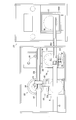
- FIG. 3 is a front view of the sealing sheet sticking apparatus
- FIG. 4 is a plan view of the sealing sheet sticking apparatus.
- the sealing sheet sticking device includes a sheet supply unit 1, a first transport mechanism 21, a liner peeling mechanism 22, a first holding table 23, a second transport mechanism 24, a sticking mechanism 25, and the like.
- the sheet supply unit 1 has a mounting table 2.
- the storage container 3 is placed on the mounting table 2.
- the storage container 3 stores, for example, a single wafer sealing sheet T cut into the shape of the semiconductor substrate W in a stacked manner.
- the first transport mechanism 21 is provided with a suction plate 26 at the lower end of a suction unit that can move horizontally and move up and down and back and forth. That is, a first movable base 28 that moves on the guide rail R1 along the frame 27 extending in the lateral direction of the apparatus main body is provided. A guide rail R2 that is horizontally held toward the front and rear of the apparatus main body is attached to the lower portion of the first movable base 28. A suction plate 26 is provided that can move up and down along a vertical frame that is suspended and supported by a second movable base 30 that can move back and forth along the guide rail R2.
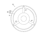
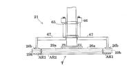
- the suction plate 26 is composed of a circular plate 26a and an annular plate 26b as shown in FIGS.
- the circular plate 26a is smaller than the outer shape of the semiconductor substrate W.
- the circular plate 26a has a heater 29a embedded therein.
- the annular plate 26b is larger than the outer shape of the semiconductor substrate W, and is configured to move up and down relative to the circular plate 26a outside the circular plate 26a.
- a boss portion 66 that moves up and down around the support shaft of the first transport mechanism 21 via a bearing 65 is provided, and the boss portion 66 is provided with three support arms 67 that extend radially in the center.
- An annular plate 26 b is attached to the lower end of each support arm 67.
- the suction plate 26 sucks and holds the outer peripheral area AR1 of the sealing sheet T by the annular plate 26b during the conveyance process, and sucks and holds the inner area AR2 of the sealing sheet T by the circular plate 26a. At this time, the sealing sheet T is held in a flat state by both the plates 26a and 26b.
- the heater 29a and the heater 29b are configured to be individually adjustable in temperature by the control unit 100.
- the circular plate 26a and the annular plate 26b may have a configuration in which suction holes are formed in a metal plate, or may be configured in a porous manner.
- the first transport mechanism 21 corresponds to the transport mechanism of the present invention
- the suction plate 26 corresponds to the holding member
- the circular plate 26a corresponds to the first sticking member
- the annular plate 26b corresponds to the second sticking member.
- the liner peeling mechanism 22 includes a peeling tape supply unit 31, a peeling unit 32, a tape recovery unit 33, and a camera 34.
- the peeling tape supply unit 31 supplies a long peeling tape TS narrower than the sealing sheet T toward the peeling unit 32.
- the peeling unit 32 includes a peeling roller 35 around which the peeling tape TS is wound.
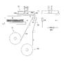
- the peeling roller 35 can be lifted and lowered to a position higher than the storage container 3. That is, in the process in which the sealing sheet T is sucked and held by the first transport mechanism 21 and is transported, the release roller 35 presses and attaches the release tape TS to the release liner S2 on the back surface of the sealing sheet T.
- the tape recovery unit 33 collects the release tape TS together with the release liner S2 peeled from the sealing sheet T by winding the release tape TS in a state of being attached to the release liner S2 on the back side of the sealing sheet T by the release roller 35.
- the release tape TS is wound around the bobbin and collected.
- the camera 34 images the sealing sheet T from which the second peeling liner S2 has been peeled off from the back surface, and transmits the image data to the control unit 100.
- the first holding table 23 is composed of a chuck table that is larger than the semiconductor substrate W.
- the first holding table 23 is configured to rotate around the vertical axis to align the semiconductor substrate W.
- the first holding table 23 is configured to reciprocate along the guide rail 38 over the mounting position of the semiconductor substrate W and the alignment position on the back side of the apparatus.
- Two cameras 39 are provided above the alignment position, take an image of the semiconductor substrate W, and transmit both image data to the control unit 100.
- the second transport mechanism 24 includes a movable base 42 that moves the apparatus on a guide rail R3 that reaches the pasting mechanism 25 side along a frame 41 that extends in the lateral direction of the apparatus main body.
- a suction plate 44 is provided at the lower end of the suction unit that can be moved up and down along a vertical frame suspended and supported by the movable table 42.
- the suction plate 44 is larger than the shape of the semiconductor substrate W. That is, the substrate transport mechanism 24 is configured to reciprocate from the first holding table 23 to a second holding table 45 described later.
- the pasting mechanism 25 includes a second holding table 45, a decompression chamber 46, and the like.
- the second holding table 45 is housed in the lower housing 46B among the upper and lower upper housings 46A and 46B constituting the decompression chamber 46.
- the lower housing 46B is configured to reciprocate between the receiving position of the semiconductor substrate W on the front side of the apparatus main body and below the upper housing 46A along the guide rail 48.
- the upper and lower housings 46A constituting the decompression chamber 46 are provided in the lift drive mechanism 50.
- the elevating drive mechanism 50 includes a movable base 53 that can be moved up and down along a rail 52 that is vertically arranged on the back of a vertical wall 51, a movable frame 54 that is supported on the movable base 53 so that the height can be adjusted, and the movable frame 53.
- An arm 55 extending forward from the frame 54 is provided.
- An upper housing 46A is mounted on a support shaft 56 that extends downward from the tip of the arm 55.
- the movable base 53 is adapted to be screwed up and down by rotating the screw shaft 57 forward and backward by a motor 58.
- a push plate 59 that can be raised and lowered is housed inside the upper housing 46A.
- a heater 60 is embedded in the pressing plate 59.
- the storage container 3 in which the sealing sheet T is stored is mounted on the mounting table 2.
- the suction plate 26 of the first transport mechanism 21 sucks the sealing sheet T and carries it out of the storage container 3 in a flat state.
- the first transport mechanism 21 transports the sealing sheet T to the liner peeling mechanism 22.
- the sealing sheet T is first conveyed above the camera 34.
- the peeling roller 35 rises to a position in the front of the transport direction that is out of the storage container 3 in the process of horizontal transport.
- the peeling tape TS wound around the peeling roller 35 is pressed against the second peeling liner S2 on the back surface side of the sealing sheet T as indicated by a chain line.
- the second release liner S2 is peeled from the sealing sheet T while winding the release tape TS at a speed synchronized with the transport speed of the first transport mechanism 21.
- the peeled second peeling liner S2 is wound and collected on the collecting bobbin together with the peeling tape TS.
- the sealing sheet T When the sealing sheet T reaches above the camera 34, the sealing sheet T is imaged. The acquired image data is transmitted to the control unit 100.
- the first transport mechanism 21 moves onto the first holding table 23 while holding the sealing sheet T by suction.
- the semiconductor substrate W is placed on the first holding table 23 substantially simultaneously with the sealing sheet T being carried out of the storage container 3.
- the first holding table 23 holding the semiconductor substrate W by suction moves to the alignment position, and the surface of the first holding table 23 is imaged by the camera 39.
- the captured image data is transmitted to the control unit 100.
- the first holding stage 23 returns to the placement position.
- the alignment of the semiconductor substrate W is performed so that the contour of the sealing sheet T obtained by the image analysis processing of the control unit 100 matches the contour of the semiconductor substrate W.
- Alignment is performed by rotating the first holding table 23 around the vertical axis.
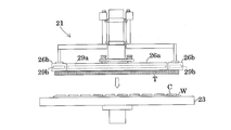
- the sealing sheet T transported by the first transport mechanism 21 is disposed to face the semiconductor substrate W as shown in FIG. Thereafter, the circular plate 26a and the annular plate 26b descend to a predetermined height while holding the sealing sheet T flat. At this time, the bottom surface of the sealing sheet T is lowered to a height at which the bottom surface contacts the surface of the semiconductor element.
- the heater 29b is operated and the annular plate 26b is slightly lowered as shown in FIG. That is, the sealing layer M is heated over a predetermined time while applying a predetermined load to the outer peripheral region of the sealing sheet T by the annular plate 26b.
- the conditions such as the load, the heating temperature, and the heating time vary depending on the properties of the thermoplastic resin composition forming the sealing layer M, but the resin composition is set to the following conditions. To do. While preventing the resin composition in the inner region AR2 softened by heating from protruding from the outside of the semiconductor substrate W, the resin composition in the outer peripheral region AR1 is semi-cured to such an extent that the adhesiveness is maintained in an uncured state.
- the resin composition forming the sealing layer M is softened by the annular plate 26a and enters while eliminating air between the semiconductor elements in the outer peripheral region, thereby sealing the semiconductor elements.
- the resin composition is semi-cured and temporarily press-bonded to the semiconductor substrate W.
- the circular plate 26a is slightly lowered to heat the inner region AR2 of the sealing layer M to soften the resin composition and to penetrate between the semiconductor elements.
- the surface of the sealing sheet T is flattened by the annular plate 26b and the circular plate 26a.
- the sealing layer M is in a temporarily press-bonded state that is not completely cured.
- the first transport mechanism 21 returns to the standby position on the mounting table 2 side.
- the semiconductor substrate W on which the sealing sheet T has been temporarily press-bonded is sucked and held by the second transport mechanism 24 and transported to the second holding table 45.
- the second transport mechanism 24 rises and returns to the first holding table 23 side.
- the second holding table 45 moves to below the upper housing 46A while holding the semiconductor substrate W by suction.
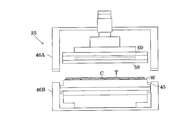
- the lower end of the upper housing 46A is lowered to a position where it comes into contact with the lower housing 46B. That is, the decompression chamber 46 is formed. Thereafter, the inside of the decompression chamber 46 is decompressed. Further, as shown in FIG. 13, the pressing plate 59 is lowered, the sealing sheet T is pressed and heated, and finally press-bonded to the semiconductor substrate W. At this point, the sealing layer M is not yet completely cured.
- the decompression chamber 46 is returned to the atmospheric pressure, and the upper housing 46A is opened.
- the lower housing 46B returns to the substrate transfer position together with the second holding table 45.
- the first release liner S1 is peeled off from the semiconductor substrate W to which the sealing sheet T is press-bonded. Thus, a series of operations for attaching the sealing sheet T to the semiconductor substrate W is completed.
- the sealing layer M in the outer peripheral area AR1 of the sealing sheet T is semi-cured first on the semiconductor substrate W, the sealing layer M in the inner area AR2 is then heated and softened. Even if pressed, the resin composition forming the sealing layer M does not protrude from the semiconductor substrate W. Therefore, contamination of the first holding table 23 holding the semiconductor substrate W and the like is suppressed.
- the present invention can also be implemented in the following forms.
- a roller with a built-in heater may be rolled along the outer peripheral area AR1 of the sealing sheet T.
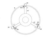
- a boss portion 66 that moves up and down around the support shaft of the first transport mechanism 21 via a bearing 65 is provided, and the boss portion 55 extends radially in the center.
- Three support arms 67 are provided.
- a roller 68 is attached to the lower end of each support arm 67 through a swing arm 69 so as to be movable up and down.
- the roller 68 is spring-biased downward.
- the roller 68 heated on the outer peripheral area AR1 of the sealing sheet T superimposed on the semiconductor substrate W is rolled to press and heat the resin composition to be semi-cured, and then the circular plate 26a.
- the resin composition in the inner region AR2 is pressed and heated to be semi-cured.
- a member having transparency and a diffusion sheet may be attached to the member to form the annular plate 26b, and an infrared LED may be provided therein.
- the sealing layer M is irradiated with infrared rays and heated by the internal infrared LED.
- the shape of the semiconductor substrate W is not limited to a circle. Therefore, the semiconductor substrate W may be a quadrangle such as a square or a rectangle.
- the outer peripheral region and the inner region may be pressurized and heated by a quadrangular annular plate and a quadrangular plate on the inner side, as in the above embodiments.
- a rectangular side edge may be covered in order with a plate with a built-in heater, and pressurized and heated.
- the sealing sheet T may be attached to the semiconductor substrate W simply by heating and softening. That is, depending on the setting conditions such as the characteristics of the resin composition constituting the sealing layer M or the heating temperature, the sealing layer M is softened only by heating without pressurizing the sealing sheet. It is also possible to paste the resin composition in between.
- the sealing sheet T is embedded in each of the circular plate 26a and the annular plate 26b before being conveyed from the storage container 3 to the first holding table 23 via the liner peeling mechanism 22.
- the heated heaters 29a and 29b may be operated to preheat to a predetermined temperature.
- the waiting time until each plate 26a, 26b reaches the set temperature and stabilizes can be shortened. In other words, the waiting time until the heating temperature of the heater is stabilized on the first holding stage 23 can be omitted.
- the outer peripheral area AR1 and the inner area AR2 of the sealing sheet T are pressed and heated by the first transport mechanism, but the configuration is not limited thereto. Therefore, after the sealing sheet T is superimposed on the semiconductor substrate W on the first holding table 23 by the first transport mechanism 21, the first transport mechanism 21 is retracted, and the apparatus including only the circular plate 26a and the annular plate 26b.
- the resin composition that forms the sealing layer M in the order of the outer peripheral area AR1 and the inner area AR2 of the sealing sheet T may be semi-cured by an apparatus including only the sealing sheet T.
- the present invention is suitable for accurately sticking a sealing sheet to a semiconductor substrate.
Landscapes
- Encapsulation Of And Coatings For Semiconductor Or Solid State Devices (AREA)
- Container, Conveyance, Adherence, Positioning, Of Wafer (AREA)
- Structures Or Materials For Encapsulating Or Coating Semiconductor Devices Or Solid State Devices (AREA)
Abstract
半導体基板Wの形状以下に切断された封止シートを第1搬送機構に備わった吸着プレートで第1保持テーブルまで搬送し、当該第1保持テーブル上の半導体基板に封止シートを重ね合わせる。吸着プレートを構成する環状プレートによって封止シートの外周領域を埋設されたヒータによって封止シートの封止層を所定の粘度の半硬化状態で半導体基板に仮圧着する。外周領域の仮圧着が完了すると、円形プレートによって封止シートの内側流域の封止層を加熱して半硬化状態で半導体基板に仮圧着する。
Description
本発明は、半導体基板上に形成された複数個の半導体素子に樹脂組成物からなる封止層の形成された封止シートを貼り付けて封止する封止シート貼付け方法および封止シート貼付け装置に関する。
1個の半導体チップの周りを枠体で囲んだ後に、樹脂を含浸させたプリプレグから成る第1の封止用樹脂シートと第2の封止用樹脂シートによって当該半導体チップの両面のそれぞれを挟み込み、半導体チップを封止して半導体装置を製造している(特許文献1を参照)。
しかしながら、上記従来方法では次のような問題が生じている。
すなわち、近年、アプリケーションの急速な進歩に伴う高密度実装の要求により、半導体装置が小型化される傾向にある。したがって、ダイシング処理によって半導体ウエハを半導体素子に分断した後に、半導体素子を個々に樹脂で封止しているので、スループットが低下し、ひいては生産効率を低下させるといった不都合が生じている。
本発明はこのような事情に鑑みてなされたものであって、半導体基板に封止シートを精度よく貼り付けることが可能な封止シート貼付け方法および封止シート貼付け装置を提供することを主たる目的とする。
そこで、本発明者たちは、当該不都合を解決するために、実験やシミュレーションを繰り返して鋭意検討した結果、以下の知見を得た。
半導体基板の全面に樹脂組成物からなる封止層の形成された枚葉の封止シートを貼り付けて硬化させた後に、当該半導体装置に分断することを試みた。そこで、封止シートを貼り付けるときに、半導体素子への密着性を高めるために封止層を加熱して軟化させていた。
しかしながら、封止シートを加熱圧着する過程で、封止層を形成する樹脂組成物が、加熱によって軟化する。すなわち、粘度が低下している状態で封止シートを半導体基板に圧着しているので、樹脂組成物が半導体基板からはみ出し、保持テーブルなどを汚染するといった問題が生じた。
この発明は、このような目的を達成するために、次のような構成をとる。
すなわち、熱可塑性の樹脂組成物からなる封止層の形成された封止シートを半導体基板に貼り付ける封止シート貼付け方法であって、
前記半導体基板の形状以下に切断された封止シートを搬送して半導体基板上に重ね合わせる搬送過程と、
前記封止シートの外周領域の封止層を加熱しながら貼り付ける第1貼付け過程と、
前記封止シートの外周領域より内側領域の封止層を加熱しながら貼り付ける第2貼付け過程と
を備えたことを特徴とする。
前記半導体基板の形状以下に切断された封止シートを搬送して半導体基板上に重ね合わせる搬送過程と、
前記封止シートの外周領域の封止層を加熱しながら貼り付ける第1貼付け過程と、
前記封止シートの外周領域より内側領域の封止層を加熱しながら貼り付ける第2貼付け過程と
を備えたことを特徴とする。
(作用・効果) この方法によれば、半導体基板に貼り付けられた封止シートの外周領域の封止層が、その内側領域に先立って硬化反応が進んだ半硬化状態にされる。したがって、加熱によって軟化している内側領域の封止層を形成している樹脂組成物は、押圧されても外周領域で半硬化した樹脂組成物によって半導体基板の外側にはみ出るのを防止される。したがって、樹保持テーブルなどが、樹脂組成物によって汚染されるのを抑制することができる。ここで、封止層を形成する樹脂組成物の特性または加熱温度などの設定条件にもよるが、加熱状態の封止シートを半導体基板に当接させるだけで半導体基板に形成された半導体素子同士の間隙に侵入して封止する。または、封止シートを加圧および加熱しながら半導体基板に貼り付けることもできる。
なお、第1貼付け過程における外周領域の封止層の加熱は、次のようにして実施することができる。
例えば、一実施形態として、外周領域を被覆する加熱器の埋設されたプレートによって当該外周領域の封止層を加圧および加熱する。他の実施形態として、加熱器の埋設されたローラを外周領域で転動させる。さらに、他の実施形態として、透過性を有するプレートにより外周領域に赤外線を照射して封止層を加熱する。なお、これら各実施形態においても、封止層を形成する樹脂組成物の特性または加熱温度の設定条件に応じて、封止シートを加熱のみ、或いは、加圧しながら加熱してもよい。
これら各実施形態において、第2貼付け過程は、例えば、内側領域を被覆する加熱器の埋設されたプレートによって当該内側領域の封止層を加熱する。この実施形態においても上記実施形態と同様に封止シートを加熱のみ、或いは、加圧しながら加熱してもよい。
これらいずれの実施形態であっても、上記方法を好適に実施することができる。
なお、上記方法において、各貼付け過程に封止シートを搬送する過程で、当該封止シートの封止層を未硬化状態に保った所定温度まで予備加熱することが好ましい。
この方法によれば、半導体基板に封止シートを貼り付けてから短時間で半硬化させることができる。
また、この発明は、このような目的を達成するために、次のような構成をとる。
すなわち、熱可塑性の樹脂組成物からなる封止層の形成された封止シートを半導体基板に貼り付ける封止シート貼付け装置であって、
前記半導体基板を保持する保持テーブルと、
前記半導体基板の形状以下に切断された封止シートを保持部材で保持して保持テーブル上の半導体基板に重ね合わせる搬送機構と、
前記半導体基板に重ね合わせた封止シートの外周領域を加熱して貼り付ける第1貼付け部材と、
前記封止シートの外周領域より内側領域を加熱して貼り付ける第2貼付け部材と
を備えたことを特徴とする。
前記半導体基板を保持する保持テーブルと、
前記半導体基板の形状以下に切断された封止シートを保持部材で保持して保持テーブル上の半導体基板に重ね合わせる搬送機構と、
前記半導体基板に重ね合わせた封止シートの外周領域を加熱して貼り付ける第1貼付け部材と、
前記封止シートの外周領域より内側領域を加熱して貼り付ける第2貼付け部材と
を備えたことを特徴とする。
この構成によれば、半導体基板上の封止シートの外周領域の封止層のみが、第1貼付け部材によって加熱されて硬化反応が進んだ半硬化状態にされる。封止シートの内側領域は、第2貼付け部材によって加熱された硬化される。したがって、上記方法を好適に実施することができる。
この構成において、第1貼付け部材は、封止シートの外周領域を被覆する加熱器の埋設されたプレートであり、
前記第2貼付け部材は、封止シートの内側領域を被覆する加熱器の埋設されたプレートで構成される。
前記第2貼付け部材は、封止シートの内側領域を被覆する加熱器の埋設されたプレートで構成される。
さらに好ましくは、第1貼付け部材を構成するプレートは、搬送機構に備わった半導体基板の外形より小さい保持部材の外周で昇降する加熱器の埋設された環状プレートで構成されており、
第2貼り付け部材は、保持部材に加熱器を埋設して構成される。
第2貼り付け部材は、保持部材に加熱器を埋設して構成される。
この構成によれば、搬送機構によって封止シートを半導体基板に貼り付けることができるので、貼付け処理の専用装置を省くことができる。すなわち、装置を小型化することができる。
本発明の封止シート貼付け方法および封止シート貼付け装置によれば、半導体基板に貼り付けた封止シートの外周領域の封止層を最初に硬化反応を進めて半硬化状態にさせるので、封止シートの内側領域で軟化された封止層を形成する樹脂組成物が押圧によって半導体基板からはみ出るのを抑制される。したがって、樹脂組成物によって保持テーブルなどが汚染されるのを抑制することができる。
1 … シート供給部
3 … 収納容器
21 … 第1搬送機構
22 … 剥離機構
23 … 第1保持テーブル
24 … 第2搬送機構
26 … 吸着プレート
26a… 円形プレート
26b… 環状プレート
25 … 貼付け機構
29a… ヒータ
29b… ヒータ
100 … 制御部
T … 封止シート
C … 半導体素子
M … 封止層
S1、S2…第1および第2剥離ライナ
W … 半導体基板
3 … 収納容器
21 … 第1搬送機構
22 … 剥離機構
23 … 第1保持テーブル
24 … 第2搬送機構
26 … 吸着プレート
26a… 円形プレート
26b… 環状プレート
25 … 貼付け機構
29a… ヒータ
29b… ヒータ
100 … 制御部
T … 封止シート
C … 半導体素子
M … 封止層
S1、S2…第1および第2剥離ライナ
W … 半導体基板
以下、図面を参照して本発明の一実施例を説明する。表面に複数個の半導体素子が形成された半導体基板に、樹脂組成物からなる封止層の形成された封止シートを貼り付ける場合を例に取って説明する。
<封止シート>
封止シートTは、例えば、図1および図2に示すように、長尺の封止シートTを巻き回した原反ロールまたは当該原反ロールから所定形状の枚様体に切断して供給される。また、当該封止シートTは、封止層Mの両面に保護用の第1剥離ライナS1および第2剥離ライナS2が添設されている。
封止シートTは、例えば、図1および図2に示すように、長尺の封止シートTを巻き回した原反ロールまたは当該原反ロールから所定形状の枚様体に切断して供給される。また、当該封止シートTは、封止層Mの両面に保護用の第1剥離ライナS1および第2剥離ライナS2が添設されている。
封止層Mは、封止材料からシート形状に形成されている。封止材料としては、例えば、熱硬化性シリコーン樹脂、エポキシ樹脂、熱硬化性ポリイミド樹脂、フェノール樹脂、ユリア樹脂、メラミン樹脂、不飽和ポリエステル樹脂、ジアリルフタレート樹脂、熱硬化性ウレタン樹脂、などの熱硬化性樹脂が挙げられる。また、封止材料として、上記した熱硬化性樹脂と、添加剤を適宜の割合で含有する熱硬化性樹脂組成物を挙げることもできる。
添加剤としては、例えば、充填剤、蛍光体などが挙げられる。充填剤としては、例えば、シリカ、チタニア、タルク、アルミナ、窒化アルミニウム、窒化ケイ素などの無機微粒子、例えば、シリコーン粒子、などの有機微粒子などが挙げられる。蛍光体は、波長変換機能を有しており、例えば、青色光を黄色光に変換することのできる黄色蛍光体、青色光を赤色光に変化することのできる赤色蛍光体などを挙げることができる。黄色蛍光体としては、例えば、Y3Al5O12:Ce(YAG(イットリウム・アルミニウム・ガーネット):Ce)などのガーネット型蛍光体が挙げられる。赤色蛍光体としては、例えば、CaAlSiN3:Eu、CaSiN2:Euなどの窒化物蛍光体などが挙げられる。
封止層Mは、半導体素子を封止する前において、半固形状に調整されており、具体的には、封止材料が熱硬化性樹脂を含有する場合には、例えば、完全硬化(Cステージ化)する前、つまり、半硬化(Bステージ)状態で調整されている。
封止層Mの寸法は、半導体素子および基板の寸法に応じて適宜に設定されている。具体的には、封止シートが長尺のシートとして用意される場合における封止層の左右方向における長さ、つまり、幅は、例えば、100mm以上、好ましくは、200mm以上であり、例えば、1500mm以下、好ましくは、700mm以下である。また、封止層の厚みは、半導体素子に寸法に対応して適宜に設定され、例えば、30μm以上、好ましくは、100μm以上であり、また、例えば、3000μm以下、好ましくは、1000μm以下である。
第1剥離ライナS1および第2剥離ライナS2は、例えば、ポリエチレンシート、ポリエステルシート(PETなど)、ポリスチレンシート、ポリカーボネートシート、ポリイミドシートなどのポリマーシート、例えば、セラミックシート、例えば、金属箔などが挙げられる。剥離ライナにおいて、封止層と接触する接触面には、フッ素処理などの離型処理を施すこともできる。第1剥離ライナおよび第2剥離ライナの寸法は、剥離条件に応じて適宜に設定され、厚みが、例えば、15μm以上、好ましくは、25μm以上であり、また、例えば、125μm以下、好ましくは、75μm以下である。
<封止シート貼付け装置>
図3は封止シート貼付け装置の正面図、図4は、封止シート貼付け装置の平面図である。
封止シート貼付け装置は、シート供給部1、第1搬送機構21、ライナ剥離機構22、第1保持テーブル23、第2搬送機構24および貼付け機構25などから構成されている。
シート供給部1は、載置台2を有する。載置台2に収納容器3が載置される。当該収納容器3は、例えば、半導体基板Wの形状に切断された枚葉の封止シートTを積層収納している。
第1搬送機構21は、前後左右に水平移動および昇降可能な吸着ユニットの下端に吸着プレート26を備えている。すなわち、装置本体の横方向に伸びるフレーム27に沿ったガイドレールR1上を移動する第1可動台28を備える。装置本体の前後に向けて水平保持されたガイドレールR2が第1可動台28の下部に装着されている。ガイドレールR2に沿って前後に移動可能な第2可動台30に懸垂支持された縦フレームに沿って昇降可能な吸着プレート26を備えている。
吸着プレート26は、図5および図6に示すように、円形プレート26aと環状プレート26bとから構成されている。
円形プレート26aは、半導体基板Wの外形よりも小形である。また、当該円形プレート26aは、内部にヒータ29aが埋設されている。
環状プレート26bは、半導体基板Wの外形よりも大形であり、円形プレート26aの外側で当該円形プレート26aに対して相対的に昇降するように構成されている。例えば、ベアリング65を介して第1搬送機構21の支軸周りに昇降および回転するボス部66を備えるとともに、当該ボス部66に、中心に径方向に延伸する3本の支持アーム67を備える。各支持アーム67の下端に環状プレート26bが装着されている
したがって、吸着プレート26は、搬送過程で環状プレート26bによって封止シートTの外周領域AR1を吸着保持し、円形プレート26aによって封止シートTの内側領域AR2を吸着保持する。このとき、両プレート26a、26bによって封止シートTは平坦な状態で保持されている。
ヒータ29aおよびヒータ29bは、制御部100によって個々に温度調整が可能に構成されている。
円形プレート26aおよび環状プレート26bは、金属製のプレートに吸引孔を形成した構成であってもよいし、多孔質で構成してもよい。
なお、第1搬送機構21は本発明の搬送機構に、吸着プレート26は保持部材に、円形プレート26aは第1貼付け部材に、環状プレート26bは第2貼付け部材にそれぞれ相当する。
ライナ剥離機構22は、図7に示すように、剥離テープ供給部31、剥離ユニット32、テープ回収部33およびカメラ34から構成される。
剥離テープ供給部31は、封止シートTよりも幅の狭い長尺の剥離テープTSを剥離ユニット32に向けて供給する。
剥離ユニット32は、剥離テープTSを巻き回される剥離ローラ35を備えている。当該剥離ローラ35は、昇降可能であり、収納容器3よりも高い位置まで上昇する。すなわち、封止シートTが第1搬送機構21によって吸着保持されて搬送される過程で、剥離ローラ35は、封止シートTの裏面の剥離ライナS2に剥離テープTSを押圧して貼り付ける。
テープ回収部33は、剥離ローラ35によって封止シートTの裏面側の剥離ライナS2に貼り付けられた状態で剥離テープTSを巻き取ることにより、封止シートTから剥離された剥離ライナS2とともに回収ボビンに剥離テープTSを巻き取り回収する。
カメラ34は、裏面から第2剥離ライナS2の剥離された封止シートTを撮像し、当該画像データを制御部100に送信する。
図3および図4に示すように、第1保持テーブル23は、半導体基板Wよりも大形のチャックテーブルで構成されている。また、第1保持テーブル23は、縦軸周りに回転し、半導体基板Wのアライメントを行うよう構成されている。さらに、第1保持テーブル23は、ガイドレール38に沿って半導体基板Wの載置位置と装置奥側のアライメント位置とにわたって往復移動するように構成されている。
アライメント位置の上方には、2台のカメラ39が配備されており、半導体基板Wを撮像し、両画像データを制御部100に送信する。
第2搬送機構24は、装置本体の横方向に伸びるフレーム41に沿って貼付け機構25側まで達するガイドレールR3上を装置移動する可動台42を備える。当該可動台42に懸垂支持された縦フレームに沿って昇降可能な吸着ユニットの下端に吸着プレート44を備えている。吸着プレート44は、半導体基板Wの形状以上の大きさを有する。すなわち、基板搬送機構24は、第1保持テーブル23から後述する第2保持テーブル45までを往復移動するよう構成されている。
貼付け機構25は、第2保持テーブル45および減圧室46などから構成されている。
第2保持テーブル45は、図8に示すように、減圧室46を構成する上下一対の上ハウジング46Aと下ハウジング46Bのうち、下ハウジング46Bに収納されている。
また、下ハウジング46Bは、ガイドレール48に沿って、装置本体の前側の半導体基板Wの受け取り位置と上ハウジング46Aの下方の間を往復移動するよう構成されている。
減圧室46を構成する上ハウジング46Aには、昇降駆動機構50に備えてられている。この昇降駆動機構50は、縦壁51の背部に縦向きに配置されたレール52に沿って昇降可能な可動台53、この可動台53に高さ調節可能に支持された可動枠54、この可動枠54から前方に向けて延出されたアーム55を備えている。このアーム55の先端部から下方に延出する支軸56に上ハウジング46Aが装着されている。
可動台53は、ネジ軸57をモータ58によって正逆転することでねじ送り昇降されるようになっている。また、上ハウジング46Aの内部には、昇降可能な押圧プレート59が内装されている。当該押圧プレート59には、ヒータ60が埋設されている。
<封止シート貼付け処理>
次に、上記封止シート貼付け装置によって半導体基板に封止シートを貼り付ける一連の動作について詳述する。
次に、上記封止シート貼付け装置によって半導体基板に封止シートを貼り付ける一連の動作について詳述する。
封止シートTの収納された収納容器3が、載置台2に載置される。第1搬送機構21の吸着プレート26が、封止シートTを吸着して平坦な状態で収納容器3から搬出する。第1搬送機構21は、封止シートTをライナ剥離機構22へと搬送する。
この搬送過程で、封止シートTは、先ずカメラ34の上方に搬送される。このとき、図7に示すように、水平搬送される過程で収納容器3から外れた搬送方向の前方の位置に剥離ローラ35が上昇してくる。当該剥離ローラ35に巻き回された剥離テープTSが、鎖線で示すように、封止シートTの裏面側の第2剥離ライナS2に押圧される。その後、第1搬送機構21の搬送速度と同調した速度で剥離テープTSを巻き取りながら、第2剥離ライナS2を封止シートTから剥離する。剥離された第2剥離ライナS2は、剥離テープTSごと回収ボビンに巻き取り回収される。
カメラ34の上方に封止シートTが達すると、封止シートTが撮像される。取得された画像データは、制御部100に送信される。撮像処理が完了すると、第1搬送機構21は、封止シートTを吸着保持したまま、第1保持テーブル23上へと移動する。
封止シートTが、収納容器3から搬出される略同時に、第1保持テーブル23に半導体基板Wが載置される。半導体基板Wを吸着保持した第1保持テーブル23は、アライメント位置に移動し、カメラ39によって表面が撮像される。撮像された画像データは、制御部100へと送信される。
撮像処理が完了すると、第1保持ステージ23は、載置位置に戻る。ここで、制御部100の画像解析処理により求めた封止シートTの輪郭と半導体基板Wの輪郭とが合致するように、半導体基板Wのアライメントを行う。第1保持テーブル23を縦軸周りに回転させてアライメントを行う。
半導体基板Wのアライメントが完了すると、第1搬送機構21によって搬送されてきた封止シートTが、図9に示すように、半導体基板Wに対向配置される。その後、円形プレート26aおよび環状プレート26bが、封止シートTを平坦に保持したまま所定高さまで下降する。このとき、封止シートTの底面が、半導体素子の表面に接触する高さまで下降する。
次に、ヒータ29bを作動させるとともに、図10に示すように、環状プレート26bを僅かに下降させる。すなわち、環状プレート26bによって、所定の荷重を封止シートTの外周領域にかけながら所定時間をかけて封止層Mを加熱する。なお、荷重、加熱温度および加熱時間などの条件は、封止層Mを形成する熱可塑性の樹脂組成物の特性に応じて異なるが、樹脂組成物が、次のような状態になる条件に設定する。加熱によって軟化する内側領域AR2の樹脂組成物が半導体基板Wの外側からはみ出るのを防止するとともに、未硬化状態で接着性を維持し続ける程度まで外周領域AR1の樹脂組成物を半硬化させる。
環状プレート26aによって封止層Mを形成する樹脂組成物が軟化して外周領域の半導体素子間のエアーを排除しながら侵入し、半導体素子を封止する。所定時間が経過すると、樹脂組成物は、半硬化して半導体基板Wに仮圧着される。
図11に示すように、円形プレート26aを僅かに下降させて封止層Mの内側領域AR2を加熱して樹脂組成物を軟化させ、半導体素子間に侵入させてゆく。ことのき、封止シートTの表面は、環状プレート26bおよび円形プレート26aによって平坦に矯正されている。所定時間経過して樹脂組成物が半硬化されると、環状プレート26bおよび円形プレート26aを上昇させて加圧および加熱を解除する。
なお、この時点で、封止層Mは、完全に硬化していない仮圧着された状態にある。封止シートTの仮圧着が完了すると、第1搬送機構21は、載置台2側の待機位置に戻る。
封止シートTが仮圧着された半導体基板Wは、第2搬送機構24によって吸着保持され、第2保持テーブル45に搬送される。
半導体基板Wが第2保持テーブル45に載置されると、第2搬送機構24は上昇して第1保持テーブル23側に戻る。第2保持テーブル45は、半導体基板Wを吸着保持したまま、上ハウジング46Aの下方まで移動する。
図12に示すように、上ハウジング46Aの下端が下ハウジング46Bに当接する位置まで下降する。つまり、減圧室46を形成する。その後、減圧室46内を減圧する。さらに、図13に示すように、押圧プレート59を下降させて封止シートTを押圧および加熱して半導体基板Wに本圧着する。この時点で、封止層Mは、未だに完全に硬化していない状態である。
本圧着が完了すると、減圧室46内を大気圧まで戻して上ハウジング46Aを開放する。下ハウジング46Bは、第2保持テーブル45ごと基板の受け渡し位置まで戻る。封止シートTの本圧着された半導体基板Wは、第1剥離ライナS1が剥離される。以上で半導体基板Wに封止シートTを貼り付ける一連の動作が完了する。
上記実施例装置によれば、半導体基板Wに封止シートTの外周領域AR1の封止層Mのみを先だって半硬化させるので、その後に内側領域AR2の封止層Mを加熱して軟化させて押圧しても封止層Mを形成する樹脂組成物が半導体基板Wからはみ出ることがない、したがって、半導体基板Wを保持している第1保持テーブル23などの汚染が抑制される。
なお、本発明は以下のような形態で実施することもできる。
(1)上記実施例において、第1搬送機構21に備わった環状プレート26bに代えて、封止シートTの外周領域AR1に沿ってヒータ内蔵のローラを転動させてもよい。
例えば、図14および図15に示すように、ベアリング65を介して第1搬送機構21の支軸周りに昇降および回転するボス部66を備えるとともに、当該ボス部55に、中心に径方向に延伸する3本の支持アーム67を備える。各支持アーム67の下端には、ローラ68が揺動アーム69を介して上下移動可能に装着されている。なお、ローラ68は、下向きにバネ付勢されている。
この構成は、半導体基板Wに重ね合わせた封止シートTの外周領域AR1上で加熱されたローラ68を転動させて樹脂組成物を加圧および加熱して半硬化させた後に、円形プレート26aによって内側領域AR2の樹脂組成物を加圧および加熱して半硬化させることになる。
(2)上記各実施例装置において、透過性を有する部材および当該部材に拡散シートを貼り付けて環状プレート26bを構成するとともに、その内部に赤外線LEDを備えた構成であってもよい。
すなわち、環状プレート26bによって封止シートTを押圧しつつ、内部の赤外線LEDによって赤外線を封止層Mに照射して加熱する。
(3)上記各実施例装置において、半導体基板Wの形状は、円形に限定されない。したがって、半導体基板Wは、正方形または長方形などの四角形であってもよい。
半導体基板Wが四角形の場合、上記各実施例と同様に、四角形状の環状プレートとその内側に四角形のプレートによって外周領域と内側領域のそれぞれを加圧および加熱すればよい。
また、ヒータ内蔵のプレートで四角形の側縁を順番に被覆して加圧および加熱するよう構成してもよい。
(4)上記各実施例装置において、封止シートTを加熱して軟化させるだけで半導体基板Wに貼り付けるようにしてもよい。すなわち、封止層Mを構成する樹脂組成物の特性または加熱温度などの設定条件によっては、封止シートを加圧せずに、加熱のみで封止層Mを軟化させて半導体素子C同士の間に樹脂組成物を侵入させて貼り付けることもできする。
(5)上記各実施例装置において、封止シートTは、収納容器3からライナ剥離機構22を経由して第1保持テーブル23に搬送させるまでに、円形プレート26aおよび環状プレート26bのそれぞれに埋設されたヒータ29a、29bを作動させて所定温度まで予備加熱してもよい。
この場合、各プレート26a、26bが、設定温度に到達して安定するまでの待ち時間を短縮することができる。換言すれば、第1保持ステージ23上でヒータの加熱温度が安定するまでの待ち時間を省くことができる。
(6)上記各実施例において、封止シートTの外周領域AR1と内側領域AR2の加圧および加熱を第1搬送機構で行っていたが当該構成に限定されない。したがって、第1搬送機構21によって第1保持テーブル23上の半導体基板Wに封止シートTを重ね合わせた後に当該第1搬送機構21を退避させ、円形プレート26aのみを備えた装置と環状プレート26bのみを備えた装置によって封止シートTの外周領域AR1と内側領域AR2の順番にその封止層Mを形成する樹脂組成物を半硬化させてもよい。
以上のように、本発明は、半導体基板に封止シートを精度よく貼り付けることができるのに適している。
Claims (10)
- 熱可塑性の樹脂組成物からなる封止層の形成された封止シートを半導体基板に貼り付ける封止シート貼付け方法であって、
前記半導体基板の形状以下に切断された封止シートを搬送して半導体基板上に重ね合わせる搬送過程と、
前記封止シートの外周領域の封止層を加熱しながら貼り付ける第1貼付け過程と、
前記封止シートの外周領域より内側領域の封止層を加熱しながら貼り付ける第2貼付け過程と
を備えたことを特徴とする封止シート貼付け方法。 - 請求項1に記載の封止シート貼付け方法において、
前記第1貼付け過程は、外周領域を被覆する加熱器の埋設されたプレートによって当該外周領域の封止層を加圧および加熱し、
前記第2貼付け過程は、内側領域を被覆する加熱器の埋設されたプレートによって当該内側領域の封止層を加圧および加熱する
ことを特徴とする封止シート貼付け方法。 - 請求項1に記載の封止シート貼付け方法において、
前記第1貼付け過程は、加熱器の埋設されたローラを外周領域で転動させて封止層を加圧および加熱し、
前記第2貼付け過程は、内側領域を被覆する加熱器の埋設されたプレートによって当該内側領域の封止層を加圧および加熱する
ことを特徴とする封止シート貼付け方法。 - 請求項1に記載の封止シート貼付け方法において、
前記第1貼付け過程は、透過性を有するプレートで外周領域を加圧した状態で赤外線を照射して封止層を加熱し、
前記第2貼付け過程は、内側領域を被覆する加熱器の埋設されたプレートによって当該内側領域の封止層を加熱する
ことを特徴とする封止シート貼付け方法。 - 請求項1に記載の封止シート貼付け方法において、
前記各貼付け過程に封止シートを搬送する過程で、当該封止シートの封止層を未硬化状態に保った所定温度まで予備加熱する
ことを特徴とする封止シート貼付け方法。 - 熱可塑性の樹脂組成物からなる封止層の形成された封止シートを半導体基板に貼り付ける封止シート貼付け装置であって、
前記半導体基板を保持する保持テーブルと、
前記半導体基板の形状以下に切断された封止シートを保持部材で保持して保持テーブル上の半導体基板に重ね合わせる搬送機構と、
前記半導体基板に重ね合わせた封止シートの外周領域を加熱して貼り付ける第1貼付け部材と、
前記封止シートの外周領域より内側領域を加熱して貼り付ける第2貼付け部材と
を備えたことを特徴とする封止シート貼付け装置。 - 請求項6に記載の封止シート貼付け装置において、
前記第1貼付け部材は、封止シートの外周領域を被覆する加熱器の埋設されたプレートであり、
前記第2貼付け部材は、封止シートの内側領域を被覆する加熱器の埋設されたプレートである
ことを特徴とする封止シート貼付け装置。 - 請求項7に記載の封止シート貼付け装置において、
前記第1貼付け部材を構成するプレートは、搬送機構に備わった半導体基板の外形より小さい保持部材の外周で昇降する加熱器の埋設された環状プレートで構成されており、
前記第2貼付け部材は、保持部材に加熱器を埋設して構成されている
ことを特徴とする封止シート貼付け装置。 - 請求項6に記載の封止シート貼付け装置において、
前記第1貼付け部材は、外周領域を転動するローラに加熱器を埋設して構成されている
ことを特徴とする封止シート貼付け装置。 - 請求項6に記載の封止シート貼付け装置において、
前記第1貼付け部材は、外周領域を被覆する透過性を有するプレートと、
当該プレートを介して当該外周領域に赤外線を照射する投光器とから構成されている
ことを特徴とする封止シート貼付け装置。
Applications Claiming Priority (2)
| Application Number | Priority Date | Filing Date | Title |
|---|---|---|---|
| JP2013095331A JP2014216606A (ja) | 2013-04-30 | 2013-04-30 | 封止シート貼付け方法および封止シート貼付け装置 |
| JP2013-095331 | 2013-04-30 |
Publications (1)
| Publication Number | Publication Date |
|---|---|
| WO2014178266A1 true WO2014178266A1 (ja) | 2014-11-06 |
Family
ID=51843401
Family Applications (1)
| Application Number | Title | Priority Date | Filing Date |
|---|---|---|---|
| PCT/JP2014/060334 Ceased WO2014178266A1 (ja) | 2013-04-30 | 2014-04-09 | 封止シート貼付け方法および封止シート貼付け装置 |
Country Status (3)
| Country | Link |
|---|---|
| JP (1) | JP2014216606A (ja) |
| TW (1) | TW201501253A (ja) |
| WO (1) | WO2014178266A1 (ja) |
Cited By (1)
| Publication number | Priority date | Publication date | Assignee | Title |
|---|---|---|---|---|
| CN116613093A (zh) * | 2023-06-28 | 2023-08-18 | 驰思(珠海)科技有限公司 | 集成电路芯片设计用封装装置 |
Families Citing this family (2)
| Publication number | Priority date | Publication date | Assignee | Title |
|---|---|---|---|---|
| JP7463036B2 (ja) * | 2020-08-21 | 2024-04-08 | 株式会社ディスコ | シート貼着方法及びシート貼着装置 |
| CN114501979A (zh) * | 2021-12-09 | 2022-05-13 | 宁波祈禧智能科技股份有限公司 | 一种智能家电线路板加工用贴片设备 |
Citations (5)
| Publication number | Priority date | Publication date | Assignee | Title |
|---|---|---|---|---|
| JPH01300531A (ja) * | 1988-05-30 | 1989-12-05 | Seikosha Co Ltd | 半導体素子の封止方法 |
| JP2000349114A (ja) * | 1999-06-07 | 2000-12-15 | Matsushita Electric Ind Co Ltd | 半導体装置の製造方法および半導体装置 |
| JP2001156088A (ja) * | 1999-11-26 | 2001-06-08 | Fujikura Ltd | 半導体装置およびその製造方法 |
| JP2003078069A (ja) * | 2001-09-05 | 2003-03-14 | Sony Corp | マルチチップモジュール作製用の疑似ウエハ、及びその作製方法 |
| JP2012142443A (ja) * | 2010-12-28 | 2012-07-26 | Fujitsu Ltd | 積層ウエハ、樹脂封止方法、及び半導体装置の製造方法 |
-
2013
- 2013-04-30 JP JP2013095331A patent/JP2014216606A/ja active Pending
-
2014
- 2014-04-09 WO PCT/JP2014/060334 patent/WO2014178266A1/ja not_active Ceased
- 2014-04-29 TW TW103115262A patent/TW201501253A/zh unknown
Patent Citations (5)
| Publication number | Priority date | Publication date | Assignee | Title |
|---|---|---|---|---|
| JPH01300531A (ja) * | 1988-05-30 | 1989-12-05 | Seikosha Co Ltd | 半導体素子の封止方法 |
| JP2000349114A (ja) * | 1999-06-07 | 2000-12-15 | Matsushita Electric Ind Co Ltd | 半導体装置の製造方法および半導体装置 |
| JP2001156088A (ja) * | 1999-11-26 | 2001-06-08 | Fujikura Ltd | 半導体装置およびその製造方法 |
| JP2003078069A (ja) * | 2001-09-05 | 2003-03-14 | Sony Corp | マルチチップモジュール作製用の疑似ウエハ、及びその作製方法 |
| JP2012142443A (ja) * | 2010-12-28 | 2012-07-26 | Fujitsu Ltd | 積層ウエハ、樹脂封止方法、及び半導体装置の製造方法 |
Cited By (1)
| Publication number | Priority date | Publication date | Assignee | Title |
|---|---|---|---|---|
| CN116613093A (zh) * | 2023-06-28 | 2023-08-18 | 驰思(珠海)科技有限公司 | 集成电路芯片设计用封装装置 |
Also Published As
| Publication number | Publication date |
|---|---|
| JP2014216606A (ja) | 2014-11-17 |
| TW201501253A (zh) | 2015-01-01 |
Similar Documents
| Publication | Publication Date | Title |
|---|---|---|
| JP5334135B2 (ja) | 積層装置 | |
| TW201203336A (en) | Method for manufacturing semiconductor device | |
| WO2014178266A1 (ja) | 封止シート貼付け方法および封止シート貼付け装置 | |
| WO2014167947A1 (ja) | 半導体装置の製造方法 | |
| WO2014167949A1 (ja) | 封止シート貼付け方法および封止シート貼付け装置 | |
| TW201501215A (zh) | 密封片貼附方法及密封片貼附裝置 | |
| JP2009246196A (ja) | シート貼付装置及び貼付方法 | |
| JP2014229790A (ja) | 封止シート貼付け方法 | |
| WO2015087763A1 (ja) | 封止シート貼付け方法 | |
| WO2014178267A1 (ja) | 封止シート貼付け方法および封止シート貼付け装置 | |
| WO2014178269A1 (ja) | 封止シート貼付け方法 | |
| JP2014229791A (ja) | 封止シート貼付け方法 | |
| CN100433246C (zh) | 接合装置、接合方法和用于制造半导体器件的方法 | |
| JP2015115346A (ja) | 封止シート貼付け方法 | |
| JP2006100762A (ja) | 固体撮像装置の製造方法 | |
| JP2015119040A (ja) | 封止シート貼付け方法 | |
| TW201501254A (zh) | 密封片貼附方法及密封片貼附裝置 | |
| JP2015115348A (ja) | 封止シート貼付け方法 | |
| WO2014119446A1 (ja) | 半導体装置の製造方法および製造装置 | |
| WO2014119445A1 (ja) | 半導体装置の製造方法および製造装置 | |
| JP2024106774A (ja) | 保護シート配設方法および保護シート |
Legal Events
| Date | Code | Title | Description |
|---|---|---|---|
| 121 | Ep: the epo has been informed by wipo that ep was designated in this application |
Ref document number: 14792036 Country of ref document: EP Kind code of ref document: A1 |
|
| NENP | Non-entry into the national phase |
Ref country code: DE |
|
| 122 | Ep: pct application non-entry in european phase |
Ref document number: 14792036 Country of ref document: EP Kind code of ref document: A1 |