WO2014174635A1 - Ledバックライト駆動回路、及びledバックライト故障検出方法 - Google Patents
Ledバックライト駆動回路、及びledバックライト故障検出方法 Download PDFInfo
- Publication number
- WO2014174635A1 WO2014174635A1 PCT/JP2013/062225 JP2013062225W WO2014174635A1 WO 2014174635 A1 WO2014174635 A1 WO 2014174635A1 JP 2013062225 W JP2013062225 W JP 2013062225W WO 2014174635 A1 WO2014174635 A1 WO 2014174635A1
- Authority
- WO
- WIPO (PCT)
- Prior art keywords
- led
- led array
- current
- voltage
- led backlight
- Prior art date
- Legal status (The legal status is an assumption and is not a legal conclusion. Google has not performed a legal analysis and makes no representation as to the accuracy of the status listed.)
- Ceased
Links
Images





Classifications
-
- G—PHYSICS
- G09—EDUCATION; CRYPTOGRAPHY; DISPLAY; ADVERTISING; SEALS
- G09G—ARRANGEMENTS OR CIRCUITS FOR CONTROL OF INDICATING DEVICES USING STATIC MEANS TO PRESENT VARIABLE INFORMATION
- G09G3/00—Control arrangements or circuits, of interest only in connection with visual indicators other than cathode-ray tubes
- G09G3/20—Control arrangements or circuits, of interest only in connection with visual indicators other than cathode-ray tubes for presentation of an assembly of a number of characters, e.g. a page, by composing the assembly by combination of individual elements arranged in a matrix no fixed position being assigned to or needed to be assigned to the individual characters or partial characters
- G09G3/34—Control arrangements or circuits, of interest only in connection with visual indicators other than cathode-ray tubes for presentation of an assembly of a number of characters, e.g. a page, by composing the assembly by combination of individual elements arranged in a matrix no fixed position being assigned to or needed to be assigned to the individual characters or partial characters by control of light from an independent source
- G09G3/3406—Control of illumination source
- G09G3/342—Control of illumination source using several illumination sources separately controlled corresponding to different display panel areas, e.g. along one dimension such as lines
- G09G3/3426—Control of illumination source using several illumination sources separately controlled corresponding to different display panel areas, e.g. along one dimension such as lines the different display panel areas being distributed in two dimensions, e.g. matrix
-
- H—ELECTRICITY
- H05—ELECTRIC TECHNIQUES NOT OTHERWISE PROVIDED FOR
- H05B—ELECTRIC HEATING; ELECTRIC LIGHT SOURCES NOT OTHERWISE PROVIDED FOR; CIRCUIT ARRANGEMENTS FOR ELECTRIC LIGHT SOURCES, IN GENERAL
- H05B45/00—Circuit arrangements for operating light-emitting diodes [LED]
- H05B45/20—Controlling the colour of the light
-
- H—ELECTRICITY
- H05—ELECTRIC TECHNIQUES NOT OTHERWISE PROVIDED FOR
- H05B—ELECTRIC HEATING; ELECTRIC LIGHT SOURCES NOT OTHERWISE PROVIDED FOR; CIRCUIT ARRANGEMENTS FOR ELECTRIC LIGHT SOURCES, IN GENERAL
- H05B45/00—Circuit arrangements for operating light-emitting diodes [LED]
- H05B45/40—Details of LED load circuits
- H05B45/44—Details of LED load circuits with an active control inside an LED matrix
- H05B45/46—Details of LED load circuits with an active control inside an LED matrix having LEDs disposed in parallel lines
-
- H—ELECTRICITY
- H05—ELECTRIC TECHNIQUES NOT OTHERWISE PROVIDED FOR
- H05B—ELECTRIC HEATING; ELECTRIC LIGHT SOURCES NOT OTHERWISE PROVIDED FOR; CIRCUIT ARRANGEMENTS FOR ELECTRIC LIGHT SOURCES, IN GENERAL
- H05B45/00—Circuit arrangements for operating light-emitting diodes [LED]
- H05B45/50—Circuit arrangements for operating light-emitting diodes [LED] responsive to malfunctions or undesirable behaviour of LEDs; responsive to LED life; Protective circuits
-
- G—PHYSICS
- G09—EDUCATION; CRYPTOGRAPHY; DISPLAY; ADVERTISING; SEALS
- G09G—ARRANGEMENTS OR CIRCUITS FOR CONTROL OF INDICATING DEVICES USING STATIC MEANS TO PRESENT VARIABLE INFORMATION
- G09G2330/00—Aspects of power supply; Aspects of display protection and defect management
- G09G2330/08—Fault-tolerant or redundant circuits, or circuits in which repair of defects is prepared
-
- G—PHYSICS
- G09—EDUCATION; CRYPTOGRAPHY; DISPLAY; ADVERTISING; SEALS
- G09G—ARRANGEMENTS OR CIRCUITS FOR CONTROL OF INDICATING DEVICES USING STATIC MEANS TO PRESENT VARIABLE INFORMATION
- G09G2330/00—Aspects of power supply; Aspects of display protection and defect management
- G09G2330/12—Test circuits or failure detection circuits included in a display system, as permanent part thereof
Definitions
- the present invention relates to an LED backlight drive circuit and an LED backlight failure detection method.
- an LED Light Emitting Diode
- This liquid crystal backlight is composed of an LED array in which a plurality of LEDs are connected in series.
- Patent Document 1 discloses a display device that can detect a failure of each of a plurality of LEDs connected in series.
- Patent Document 1 requires a failure detection component for each LED that constitutes the LED array. Therefore, there is a problem that the circuit configuration becomes complicated.
- the present invention has been made in view of the above problems, and in an LED backlight driving circuit, an LED backlight that easily detects a failure of an LED of an LED array that constitutes the LED backlight with a simple circuit configuration.
- An object of the present invention is to provide a driving circuit and a method for detecting a failure of an LED backlight.
- an LED backlight driving circuit includes a power supply circuit that supplies a driving current to each of the LED arrays that constitute a backlight of a display device, and the LED array A voltage adjusting unit that changes the voltage of the power supply circuit according to the LED array, a current changeover switch that supplies an output voltage from the voltage adjusting unit to one of the LED arrays, and a current that flows through the LED array
- a current detection unit that stores the initial current value during the initial setting operation for each LED array detected by the current detection unit, and the drive current value during the normal operation for each LED array and the storage unit.
- a failure detection method for detecting a failure of a plurality of LED arrays constituting a backlight of a liquid crystal monitor is provided between a power supply circuit and the LED array during an initial setting operation.
- an output voltage from the power supply circuit is supplied and the LED arrays are sequentially turned on, and each LED array is turned on in the initial setting lighting process.
- An initial current detection process for detecting an initial current value flowing through the LED an initial current storage process for storing an initial current value for each LED array detected in the initial current detection process in a storage unit, and the current during normal operation.
- a driving current detection process for detecting a driving current value flowing for each LED array in the lighting process during the normal operation; a driving current value for each LED array detected in the driving current detection process;
- the LED backlight driving circuit it is possible to automatically detect a failure of the LED of the LED array constituting the LED backlight.
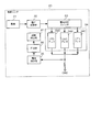
- FIG. 1 is a diagram showing a configuration of the liquid crystal monitor 30 according to the present embodiment.
- the liquid crystal monitor 30 includes a power supply 31, a voltage adjustment unit 32, a current changeover switch 33, an LED (light emitting diode) backlight 34, a current detection unit 35, a storage unit 36, and a failure detection unit 37.
- the power supply 31 supplies a drive current to each of the LED arrays 34A, 34B, 34C constituting the LED backlight 34 of the liquid crystal monitor 30.
- the voltage adjustment unit 32 changes the voltage from the power supply 31 supplied to the LED arrays 34A, 34B, and 34C.
- the LED arrays 34A, 34B, and 34C are composed of R, G, and B LEDs, respectively.
- the voltage adjusting unit 32 and the current changeover switch 33 mix and generate white by driving the RGB three primary color backlights in a time-sharing manner.
- the current switch 33 supplies the drive current from the voltage adjustment unit 32 to any of the LED arrays 34A, 34B, 34C.
- the current detector 35 detects the current flowing through the LED arrays 34A, 34B, and 34C.
- the storage unit 36 has an initial current value for each of the LED arrays 34A, 34B, 34C detected by the current detection unit 35 during the initial setting operation, and an LED array 34A, 34B detected by the current detection unit 35 during the failure detection operation. , 34C for each drive current.
- the failure detection unit 37 compares the initial current values of the LED arrays 34A, 34B, and 34C stored in the storage unit 36 with the drive current values during normal operation (when a failure is detected), and the LED arrays 34A, 34B, 34C fault is detected.
- the output voltage from the LED backlight driving voltage adjustment unit 32 is converted to the LED array 34A, 34B, 34C constituting the LED backlight 34 using the current selector switch 33. Light up sequentially. Moreover, in this embodiment, the LED backlight 34 is driven and the output voltage of the voltage adjustment part 32 is adjusted for every LED array 34A, 34B, 34C.
- the current feedback signal (initial current value) for each of the LED arrays 34A, 34B, and 34C used for the adjustment is detected by the current detection unit 35 and stored in the storage unit 36.
- the output voltage from the voltage adjustment unit 32 for driving the LED backlight is similarly used to configure the LED backlight 34 using the current selector switch 33.
- Each LED array 34A, 34B, 34C to be turned on is sequentially turned on to drive the LED backlight 34.
- the failure detection unit 37 compares the drive current passed for each of the LED arrays 34A, 34B, and 34C with the initial current value for each of the LED arrays 34A, 34B, and 34C stored in the storage unit 36. If the difference between the two matches (within a predetermined allowable range), it is determined as normal. Moreover, the failure detection part 37 will determine with the failure having generate
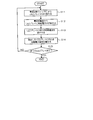
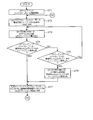
- FIG. 2 is a flowchart showing the 30 initial setting operation of the liquid crystal monitor according to the present embodiment.
- Step S11 When the initial setting operation is started, first, the current selector switch 33 switches to the LED array 34A constituting the LED backlight 34.
- Step S12 The voltage adjustment unit 32 generates a voltage for the LED array 34A in synchronization with the switching to the LED array 34A, and supplies a drive current (initial current) to the LED array 34A via the current switch 33. .
- each LED constituting the LED array 34A emits light with a luminance corresponding to the value of the flowing current.
- the current detector 35 detects the current flowing through the LED array 34A.
- the current detection unit 35 stores the current detected by the current detection unit 35 in the storage unit 36 in association with the LED 34A as an initial current value.
- Step S15 It is determined whether or not all LED arrays have been completed. If not completed (step S15; NO), the process returns to step S11. If completed (step S15; YES), the process is terminated.
- Steps S11 to S15; Second Process Next, the current selector switch 33 switches to the LED array 34B constituting the LED backlight 34.
- the voltage adjustment unit 32 generates a voltage for the LED array 34B in synchronization with the switching to the LED array 34B, and performs the same processing on the LED array 34B.
- the current detection unit 35 stores the detected current flowing in the LED 34B in the storage unit 36 in association with the LED 34B as an initial current value.
- the voltage adjustment unit 32 generates a voltage for the LED array 34C in synchronization with the switching of the current selector switch 33 to the LED array 34C, and performs the same processing on the LED array 34C.
- the current detection unit 35 stores the detected current flowing in the LED 34C in the storage unit 36 in association with the LED 34C as an initial current value.
- the reason why the drive voltages are individually set for the LED arrays 34A, 34B, and 34C is that the LED forward voltage has a larger variation in LEDs for each color than individual variations in LEDs of the same color. is there.
- the initial current values of the LED arrays 34A, 34B, and 34C are stored in the storage unit 36. Thereafter, the normal operation (failure detection operation) of the liquid crystal monitor 30 shown in FIG. 3 is executed.
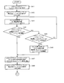
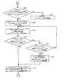
- FIG. 3 is a flowchart showing a failure detection operation of the liquid crystal monitor 30 according to the present embodiment.
- Step S21 When the failure detection operation is activated, first, the current selector switch 33 switches to the LED array 34A constituting the LED backlight 34.
- Step S22 The voltage adjustment unit 32 generates a voltage for the LED array 34A in synchronization with the switching to the LED array 34A, and supplies a drive current (initial current) to the LED array 34A via the current switch 33. . At this point, each LED constituting the LED array 34A emits light with a luminance corresponding to the value of the flowing current.
- Step S23 The current detector 35 detects the current flowing through the LED array 34A.
- Step S24 The current detection unit 35 stores the current detected by the current detection unit 35 in the storage unit 36 in association with the LED 34A as a drive current value.
- Step S25 The failure detection unit 37 compares the drive current value passed through the LED array 34A with the initial current value stored in the storage unit 36, and determines whether or not they match. If both are the same (difference is within a predetermined allowable range) (step S25; YES), the failure detection unit 37 determines that it is normal and returns to step S21. On the other hand, if both are inconsistent (difference is outside the predetermined allowable range) (step S25; NO), the failure detection unit 37 proceeds to step S26.
- Step S ⁇ b> 26 The failure detection unit 37 determines that a failure has occurred in the LED array 34 ⁇ / b> A because both are inconsistent (the difference is outside the predetermined allowable range).
- Steps S21 to S26 (second processing)
- the current selector switch 33 switches to the LED array 34B constituting the LED backlight 34.
- the voltage adjustment unit 32 generates a voltage for the LED array 34B in synchronization with the switching to the LED array 34B, and performs the same processing on the LED array 34B.
- the failure detection unit 37 compares the drive current value passed through the LED array 34B with the initial current value of the LED array 34B stored in the storage unit 36, and determines whether or not they match.
- Step S25 if both are the same (difference is within a predetermined allowable range) (Step S25; YES), it is determined as normal, and if both are the same (the difference is outside the predetermined allowable range) (Step S25) S25; NO), it is determined that a failure has occurred in the corresponding LED array 34B (step S26).
- Steps S21 to S26 (third process) Similarly, the LED array 34C constituting the LED backlight 34 is switched.
- the voltage adjustment unit 32 generates a voltage for the LED array 34C in synchronization with the switching to the LED array 34C, and performs the same processing on the LED array 34C.
- the failure detection unit 37 compares the drive current value passed through the LED array 34C with the initial current value of the LED array 34C stored in the storage unit 36, and determines whether or not they match.
- Step S25 if both are the same (difference is within a predetermined allowable range) (Step S25; YES), it is determined as normal, and if both are the same (the difference is outside the predetermined allowable range) (Step S25) S25; NO), it is determined that a failure has occurred in the corresponding LED array 34C (step S26).
- the voltage adjustment unit 32, the current changeover switch 33, and the current detection unit 35 repeatedly execute steps S21 to S26, and use the current changeover switch 33 to output the output voltage from the LED backlight drive voltage adjustment unit 32.
- the LED arrays 34A, 34B, and 35C are turned on so as to sequentially cycle.
- the failure detection unit 37 compares the drive current value passed for each of the LED arrays 34A, 34B, and 35C with the initial current value of each LED array 34A, 34B, and 35C stored in the storage unit 36, If the difference is within a predetermined allowable range, it is determined as normal. Alternatively, the failure detection unit 37 determines that a failure has occurred in the corresponding LED array if the difference is outside the predetermined allowable range.
- the LED backlight drive circuit can automatically detect the failure of the LEDs of the LED array constituting the LED backlight.
- FIG. 4 is a diagram showing the configuration of the liquid crystal monitor according to the present embodiment.
- the liquid crystal monitor 1 includes a CPU (Central Processing Unit) 11, a memory 1B, an LED backlight controller 12, a DC / DC booster circuit 13, an LED backlight 14, a current changeover switch 15, and a feedback resistor. 16, a video processing circuit 18, a liquid crystal display control circuit 19, and a liquid crystal display device 20.
- CPU Central Processing Unit
- the CPU 11 outputs a control signal to the video processing circuit 18 through the video processing circuit control signal line 104 to control the video processing circuit 18.
- the video processing circuit 18 inputs a video input signal to be displayed on the liquid crystal monitor 1 from an external device via the video input signal line 101. Further, the video processing circuit 18 controls the liquid crystal display control circuit 19 by the panel video signal generated from the video input signal via the panel video signal line 105.
- the liquid crystal display control circuit 19 generates a liquid crystal display signal for controlling each of the liquid crystal elements constituting the liquid crystal display device 20 from the input panel video signal, and sets the liquid crystal display signal line 106 to the liquid crystal display device 20. Output via.
- liquid crystal display device 20 a plurality of liquid crystal elements are arranged in a matrix, the light transmission state of each liquid crystal element is controlled by a liquid crystal display signal, and gradation control using the liquid crystal elements as pixels is performed.
- the CPU 11 outputs a backlight control signal to the LED backlight controller 12 via the backlight control signal line 102 to control the LED backlight controller 12. For example, the CPU 11 outputs a switching cycle of the current changeover switch 15 and a reference voltage value as a control value of the LED backlight 14 to the LED backlight controller 12. Since this reference voltage value is used for control for uniformizing the light emission of the LED arrays 14A, 14B, and 14C, the current value of the current (drive current) that is desired to flow through the LED arrays 14A, 14B, and 14C and the feedback resistor 16 It is set to a value obtained by multiplying the resistance value, and is set in the CPU 11 in advance.
- the LED backlight 14 is disposed opposite to the rear surface opposite to the display surface of the liquid crystal panel in which the liquid crystal elements in the liquid crystal display device 20 are disposed, and irradiates each liquid crystal element of the liquid crystal panel with light.
- a plurality of LED arrays in which a plurality of LEDs are connected in series are arranged in parallel, for example, as LED arrays 14A, 14B, and 14C as shown in FIG.
- This liquid crystal panel is configured by disposing liquid crystal elements at intersections of a plurality of data lines and a plurality of scanning lines wired in a matrix.
- the output terminal of the DC / DC booster circuit 13 and the common terminal 15 ⁇ / b> S are connected by the LED backlight current line 100.
- the switching terminal 15A is connected to the anode at the end of the LED array 14A via the LED array current line 101A
- the switching terminal 15B is connected to the anode at the end of the LED array 14B and the LED array current line 102A.
- the switching terminal 15C is connected to the anode at the end of the LED array 14C via the LED array current line 103A.
- the current changeover switch 15 is switched by a current changeover switch control signal line periodically supplied from the LED backlight controller 12 via the current changeover switch control signal line 121, and the common terminal 15S is changed over to the changeover terminals 15A, 15B, 15C. Connect to either.
- the LED array 14A has an end cathode connected to a connection point Q1 via an LED array current line 101B.
- the cathode at the end is connected to the connection point Q1 via the LED array current line 102B.
- the LED array 14C the cathode at the end is connected to the connection point Q1 via the LED array current line 103B.
- the LED arrays 14A, 14B, and 14C are configured by R, G, and B LEDs, respectively. Also.
- the LED backlight controller 12, the DC / DC booster circuit 13, and the current selector switch 15 are mixed by driving the RGB three primary color backlights in a time-sharing manner as in the first embodiment. To produce white.
- the connection point Q1 is connected to the connection point Q2 via the LED backlight current line 110.
- the feedback resistor 16 has one end connected to the connection point Q2 via the LED backlight current line 120, and the other end connected to the ground point GND. At the connection point Q2, the cathode sides of the LED arrays 14A, 14B, and 14C are connected in common. For this reason, in the second embodiment, the current flowing through each of the LED arrays 14A, 14B, and 14C is measured as the voltage across the terminals of the same feedback resistor 16.
- the LED backlight controller 12 sends a current changeover switch control signal indicating that the common terminal 15S is changed over and connected to the changeover terminals 15A, 15B, and 15C sequentially in accordance with the changeover cycle supplied from the CPU11.
- the switching operation of the current changeover switch 15 is controlled by outputting via the control signal line 121.
- each of the switching terminals 15A, 15B, and 15C is connected to the common terminal 15S in the period of the switching period, and any switching terminal is connected to the common terminal 15S. During this period, the other switching terminals are not connected.
- the LED backlight controller 12 synchronizes the common terminal 15S with the timing at which the common terminal 15S is sequentially periodically connected to any one of the switching terminals 15A, 15B, and 15C. Detection is performed via the LED backlight array current feedback signal line 111 connected to Q2.
- the LED backlight controller 12 is synchronized with the current changeover switch control signal by the current flowing through the LED array to which the output voltage of the DC / DC booster circuit 13 is applied via the changeover terminal connected to the common terminal 15S. The voltage between the terminals generated by the voltage drop of the feedback resistor 16 is measured.
- the LED backlight controller 12 sets the voltage value of the voltage output from the DC / DC booster circuit 13 so that the detected voltage across the terminals of the feedback resistor 16 is the same as the reference voltage value supplied from the CPU 11. Control. At this time, the LED backlight controller 12 outputs a DC / DC boost circuit control signal to the DC / DC boost circuit 13 via the DC / DC boost circuit control signal line 103 to the DC / DC boost circuit 13. The voltage value of the output voltage output from the / DC booster circuit 13 is controlled.
- the LED backlight controller 12 controls the DC / DC booster circuit 13 to generate a voltage for the LED array 14A when the current switch control signal is a signal for switching to the switching terminal 15A. Similarly, the LED backlight controller 12 controls the DC / DC booster circuit 13 to generate a voltage for the LED array 14B when the current changeover switch control signal is a signal for switching to the switching terminal 15B. Further, the LED backlight controller 12 controls the DC / DC booster circuit 13 to generate a voltage for the LED array 14C when the current changeover switch control signal is a signal for switching to the switching terminal 15C.
- the CPU 11 uses the current selector switch 15 to output the output voltage from the DC / DC booster circuit 13 for driving the LED backlight to each LED array 14A, 14B, 14C constituting the LED backlight 14.
- the LED backlight 14 is driven sequentially, the output voltage of the DC / DC booster circuit 13 is adjusted for each of the LED arrays 14A, 14B, and 14C, and current feedback for each of the LED arrays 14A, 14B, and 14C used for the adjustment
- the signal (initial current value) is detected by the LED backlight controller 12 and stored in the memory 1B.
- the CPU 11 uses the current selector switch 15 to output the output voltage from the DC / DC booster circuit 13 to each LED array 14A constituting the LED backlight 14;
- the LED backlight 14 is driven by sequentially lighting 14B and 14C.
- the drive current fed back from the LED backlight array current feedback signal line 111 for each of the LED arrays 14A, 14B, 14C, and the initial current value for each of the LED arrays 14A, 14B, 14C stored in the memory 1B If the difference between the two is the same (within a predetermined allowable range), it is determined to be normal, and if the difference between the two is not the same (out of the predetermined allowable range), it is determined that a failure has occurred in the corresponding LED array.
- the LED backlight drive circuit can automatically detect a failure of the LEDs of the LED arrays 14A, 14B, and 14C constituting the LED backlight 14.
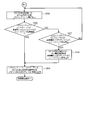
- FIGS. 4 and 5 to 7 are flowcharts showing the initial setting operation of the liquid crystal monitor according to the present embodiment.
- Step S41 When the liquid crystal monitor 1 is powered on, the liquid crystal monitor 1 enters an operating state, and the initial setting operation is activated, the CPU 11 activates the LED backlight controller 12. Next, after starting the LED backlight controller 12, the CPU 11 outputs a backlight control signal including a switching period and a reference voltage value to the LED backlight controller 12 via the backlight control signal line 102. To do.
- Step S42 The LED backlight controller 12 outputs a current changeover switch control signal for instructing connection of the common terminal 15S to the changeover terminal 15A to the current changeover switch 15 via the current changeover switch control signal line 121. To do. Next, the LED backlight controller 12 resets an internal timer in order to control the switching cycle for turning on the LED array 14A, sets the time of the switching cycle in this timer again, and starts counting of this timer. .
- Step S43 The LED backlight controller 12 activates the DC / DC booster circuit 13 and instructs to gradually increase the output voltage of the DC / DC booster circuit 13 in synchronization with the switching to the LED array 14A.
- the DC / DC boost circuit control signal is output to the DC / DC boost circuit 13 via the DC / DC boost circuit control signal line.
- the DC / DC boost circuit 13 starts a boost operation to increase the output voltage, boosts the power supply voltage, and the LED array 14A. Generate voltage.
- the DC / DC booster circuit 13 outputs the generated voltage for the LED array 14A as an output voltage to the common terminal 15S of the current changeover switch 15 via the LED backlight current line 100. Thereby, the output voltage output from the DC / DC booster circuit 13 is applied to the LED array 14A via the switching terminal 15A of the current selector switch 15 and the LED array current line 101A.
- Step S44 The LED backlight controller 12 compares the current feedback voltage of the LED array 14A fed back by the LED backlight array current feedback signal line 111 with a reference voltage (for example, a reference voltage of 0.3 [V]). .
- a reference voltage for example, a reference voltage of 0.3 [V]
- the LED backlight controller 12 advances the process to step S47 when the voltage value between the terminals and the reference voltage value match (the difference is within a predetermined allowable range) (step S44; YES).
- step S33; NO the LED backlight controller 12 advances the process to step S45.
- Step S45 The LED backlight controller 12 determines whether or not the voltage value between the terminals, that is, the feedback signal voltage value of the LED array 14A is higher than the reference voltage value. Next, the LED backlight controller 12 increases the output voltage of the DC / DC booster circuit 13 when the feedback signal voltage value of the LED array 14A is not higher than the reference voltage value, that is, when it is lower (step S45; NO). Then, the process proceeds to step S43. On the other hand, when the feedback signal voltage value of the LED array 14A is larger than the end reference voltage value (step S4; YES), the LED backlight controller 12 advances the process to step S46.
- Step S46 The LED backlight controller 12 obtains a difference voltage between the feedback signal voltage value of the LED array 14A and the reference voltage value, and performs DC / DC boosting indicating that the output voltage is reduced by this difference voltage.
- a circuit control signal is output to the DC / DC booster circuit 13, and the output voltage of the DC / DC booster circuit 13 is controlled so that the voltage value of the inter-terminal voltage matches the reference voltage value.
- the LED backlight controller 12 advances the process to step S47.
- the LED backlight controller 12 stores the value of the DC / DC boost circuit control signal at this time (the initial current value of the LED array 14A) in the LED array 1n area of the memory 1B.
- the LED backlight controller 12 controls the current changeover switch 15 by the current changeover switch control signal line 121 instructing to connect the common terminal 15S to the changeover terminal 15B, and the LED backlight current line 100 is set to the LED. Connect to array current line 102A.
- Step S49 The LED backlight controller 12 performs the same control as when the LED array 14A is turned on, generates a voltage for the LED array 14B in synchronization with the switching to the LED array 14B, and the LED array 14B. Lights up.
- Step S50 The LED backlight controller 12 compares the current feedback voltage of the LED array 14B fed back by the LED backlight array current feedback signal line 111 with a reference voltage (for example, a reference voltage of 0.3 [V]). .
- a reference voltage for example, a reference voltage of 0.3 [V]
- step S50 if the voltage value of the inter-terminal voltage matches the reference voltage value (the difference is within a predetermined allowable range) (step S50; YES), the LED backlight controller 12 advances the process to step S53. On the other hand, if the voltage value between the terminals and the reference voltage value do not match (the difference is outside the predetermined allowable range) (step S50; NO), the LED backlight controller 12 advances the process to step S51.
- Step S51 The LED backlight controller 12 determines whether or not the voltage value between the terminals, that is, the feedback signal voltage value of the LED array 14B is higher than the reference voltage value.
- the LED backlight controller 12 increases the output voltage of the DC / DC booster circuit 13. Therefore, the process proceeds to step S49.
- step S51; YES the LED backlight controller 12 advances the process to step S52.
- Step S52 The LED backlight controller 12 obtains a differential voltage between the feedback signal voltage value of the LED array 14B and the reference voltage value, and performs DC / DC boosting indicating that the output voltage is controlled to be reduced by this differential voltage.
- a circuit control signal is output to the DC / DC booster circuit 13, and the output voltage of the DC / DC booster circuit 13 is controlled so that the voltage value of the inter-terminal voltage matches the reference voltage value. Then, the LED backlight controller 12 advances the process to step S53.
- Step S53 The LED backlight controller 12 stores the value of the DC / DC booster circuit control signal at this time (the initial current value of the LED array 14B) in the LED array 2n area of the memory 1B.
- Step S54 The LED backlight controller 12 controls the current changeover switch 15 by the current changeover switch control signal line 121 instructing to connect the common terminal 15S to the changeover terminal 15C, and the LED backlight current line 100 is set to LED. Connect to array current line 103A.
- Step S55 The LED backlight controller 12 performs the same control as when the LED arrays 14A and 14B are turned on, and generates a voltage for the LED array 14C in synchronization with the switching to the LED array 14C.
- the array 14C is turned on.
- Step S56 The LED backlight controller 12 compares the current feedback voltage of the LED array 14C fed back by the LED backlight array current feedback signal line 111 with a reference voltage (for example, a reference voltage of 0.3 [V]). .
- a reference voltage for example, a reference voltage of 0.3 [V]
- step S56 if the voltage value of the inter-terminal voltage matches the reference voltage value (the difference is within a predetermined allowable range) (step S56; YES), the LED backlight controller 12 advances the process to step S59. On the other hand, if the voltage value between the terminals and the reference voltage value do not match (the difference is outside the predetermined allowable range) (step S56; NO), the LED backlight controller 12 advances the process to step S57.
- Step S57 The LED backlight controller 12 determines whether or not the voltage value between the terminals, that is, the feedback signal voltage value of the LED array 14C is higher than the reference voltage value.
- the LED backlight controller 12 increases the output voltage of the DC / DC booster circuit 13. Therefore, the process proceeds to step S55.
- step S57; YES the LED backlight controller 12 advances the process to step S58.
- Step S58 The LED backlight controller 12 obtains a differential voltage between the feedback signal voltage value of the LED array 14C and the reference voltage value, and performs DC / DC boosting indicating that the output voltage is controlled to be reduced by this differential voltage.
- a circuit control signal is output to the DC / DC booster circuit 13, and the output voltage of the DC / DC booster circuit 13 is controlled so that the voltage value of the inter-terminal voltage matches the reference voltage value. Then, the LED backlight controller 12 advances the process to step S59.
- Step S59 The LED backlight controller 12 stores the value of the DC / DC boost circuit control signal at this time (the initial current value of the LED array 14C) in the LED array 3n area of the memory 1B.
- the initial current value of the LED array 14A is stored in the LED array 1n area of the memory 1B, the initial current value of the LED array 14B is stored in the LED array 2n area, and the LED array 3n area In this case, the initial current value of the LED array 14CB is stored. Thereafter, the operation proceeds to normal operation (failure detection operation).
- the output voltage from the DC / DC booster circuit 13 for driving the LED backlight is sequentially turned on by using the current changeover switch 15 to turn on the LED arrays 14A, 14B, and 14C constituting the LED backlight 14.
- the output voltage of the DC / DC booster circuit 13 is adjusted for each of the LED arrays 14A, 14B, and 14C, and current feedback signals (drive current values) for the LED arrays 14A, 14B, and 14C used for the adjustment are stored in the memory 1B.
- the drive current value is compared with the corresponding initial current value to detect an LED failure.
- Step S71 When the failure detection operation is activated, the CPU 11 activates the LED backlight controller 12. Next, after starting the LED backlight controller 12, the CPU 11 outputs a backlight control signal including a switching period and a reference voltage value to the LED backlight controller 12 via the backlight control signal line 102. To do.
- Step S ⁇ b> 72 The LED backlight controller 12 outputs a current changeover switch control signal instructing to connect the common terminal 15 ⁇ / b> S to the changeover terminal 15 ⁇ / b> A to the current changeover switch 15 via the current changeover switch control signal line 121. To do. Next, the LED backlight controller 12 resets an internal timer in order to control the switching cycle for turning on the LED array 14A, sets the time of the switching cycle in this timer again, and starts counting of this timer. .
- the LED backlight controller 12 activates the DC / DC booster circuit 13 and instructs to gradually increase the output voltage of the DC / DC booster circuit 13 in synchronization with the switching to the LED array 14A.
- the DC / DC boost circuit control signal is output to the DC / DC boost circuit 13 via the DC / DC boost circuit control signal line.
- the DC / DC boost circuit 13 starts a boost operation to increase the output voltage, boosts the power supply voltage, and the LED array 14A. Generate voltage.
- the DC / DC booster circuit 13 outputs the generated voltage for the LED array 14A as an output voltage to the common terminal 15S of the current selector switch 15 via the LED backlight current line 100. Thereby, the output voltage output from the DC / DC booster circuit 13 is applied to the LED array 14A via the switching terminal 15A of the current selector switch 15 and the LED array current line 101A.
- Step S74 The LED backlight controller 12 compares the current feedback voltage of the LED array 14A fed back by the LED backlight array current feedback signal line 111 with a reference voltage (for example, a reference voltage of 0.3 [V]). . Then, the LED backlight controller 12 advances the process to step S77 when the voltage value of the inter-terminal voltage matches the reference voltage value (the difference is within a predetermined allowable range) (step S74; YES). On the other hand, if the voltage value between the terminals and the reference voltage value do not match (the difference is outside the predetermined allowable range) (step S74; NO), the LED backlight controller 12 advances the process to step S75.
- a reference voltage for example, a reference voltage of 0.3 [V]
- Step S75 The LED backlight controller 12 determines whether or not the voltage value between the terminals, that is, the feedback signal voltage value of the LED array 14A is higher than the reference voltage value.
- the LED backlight controller 12 increases the output voltage of the DC / DC booster circuit 13. Therefore, the process proceeds to step S73.
- step S75; YES the LED backlight controller 12 advances the process to step S76.
- Step S76 The DC backlight controller 12 obtains a difference voltage between the feedback signal voltage value of the LED array 14A and the reference voltage value, and performs DC / DC boosting indicating that the output voltage is reduced by this difference voltage.
- a circuit control signal is output to the DC / DC booster circuit 13, and the output voltage of the DC / DC booster circuit 13 is controlled so that the voltage value of the inter-terminal voltage matches the reference voltage value. Then, the LED backlight controller 12 advances the process to step S77.
- Step S77 The LED backlight controller 12 stores the value of the DC / DC booster circuit control signal at this time (the drive current value of the LED array 14A) in the LED array 1n + 1 area of the memory 1B.
- Step S78 The CPU 11 compares the value of the LED array 1n area (initial current value of the LED array 14A) in the memory 1B with the value of the LED array 1n + 1 area (drive current value of the LED array 14A). If the comparison result is the same (both differences are within a predetermined allowable range) (step S78; YES), the CPU 11 advances the process to step S80. On the other hand, if the comparison results are not equal (both differences are outside the predetermined allowable range) (step S78; NO), the process proceeds to step S79.
- Step S ⁇ b> 79 The CPU 11 detects that the LED array 14 ⁇ / b> A is out of order because the compared results are not equal (the difference between the two is outside the predetermined allowable range). (Step S80) Since the comparison results are equal (both differences are within a predetermined allowable range), the CPU 11 determines that the LED array 14A has not failed, and the LED backlight controller 12 switches the common terminal 15S to the switching terminal.
- the current changeover switch 15 is controlled by the current changeover switch control signal line 121 instructing connection to 15B, and the LED backlight current line 100 is connected to the LED array current line 102A.
- Step S81 The LED backlight controller 12 performs the same control as when the LED array 14A is turned on, generates a voltage for the LED array 14B in synchronization with the switching to the LED array 14B, and the LED array 14B. Lights up.
- Step S82 The LED backlight controller 12 compares the current feedback voltage of the LED array 14B fed back by the LED backlight array current feedback signal line 111 with a reference voltage (for example, a reference voltage of 0.3 [V]). . Then, if the voltage value of the inter-terminal voltage matches the reference voltage value (the difference is within a predetermined allowable range) (step S82; YES), the LED backlight controller 12 advances the process to step S85. On the other hand, if the voltage value of the terminal voltage does not match the reference voltage value (the difference is outside the predetermined allowable range) (step S82; NO), the LED backlight controller 12 advances the process to step S83.
- a reference voltage for example, a reference voltage of 0.3 [V]
- Step S83 The LED backlight controller 12 determines whether or not the voltage value between the terminals, that is, the feedback signal voltage value of the LED array 14B is higher than the reference voltage value. When the feedback signal voltage value of the LED array 14B is not higher than the reference voltage value, that is, when it is lower (step S83; NO), the LED backlight controller 12 increases the output voltage of the DC / DC booster circuit 13, The process proceeds to step S81. On the other hand, if the feedback signal voltage value of the LED array 14B is larger than the end reference voltage value (step S83; YES), the LED backlight controller 12 advances the process to step S84.
- Step S84 The LED backlight controller 12 obtains a difference voltage between the feedback signal voltage value of the LED array 14B and the reference voltage value, and performs DC / DC boosting indicating that the output voltage is reduced by this difference voltage.
- a circuit control signal is output to the DC / DC booster circuit 13, and the output voltage of the DC / DC booster circuit 13 is controlled so that the voltage value of the inter-terminal voltage matches the reference voltage value.
- the LED backlight controller 12 advances the process to step S85.
- Step S85 The LED backlight controller 12 stores the value of the DC / DC boost circuit control signal at this time (the drive current value of the LED array 14B) in the LED array 2n + 1 area of the memory 1B.
- Step S86 The CPU 11 compares the value of the LED array 2n area (initial current value of the LED array 14B) in the memory 1B with the value of the LED array 2n + 1 area (drive current value of the LED array 14B). Then, when the comparison results are equal (both differences are within a predetermined allowable range) (step S86; YES), the CPU 11 advances the process to step S88. On the other hand, if the comparison results are not equal (both differences are outside the predetermined allowable range) (step S86; NO), the process proceeds to step S87.
- Step S ⁇ b> 87 The CPU 11 detects that the LED array 14 ⁇ / b> B has failed because the comparison result is not equal (the difference between the two is outside the predetermined allowable range).
- Step S88 The LED backlight controller 12 controls the current changeover switch 15 by the current changeover switch control signal line 121 that instructs to connect the common terminal 15S to the changeover terminal 15C. Connect to array current line 103A.
- Step S89 The LED backlight controller 12 performs the same control as when the LED arrays 14A and 14B are turned on, generates a voltage for the LED array 14C in synchronization with the switching to the LED array 14C, and The array 14C is turned on.
- Step S90 The LED backlight controller 12 compares the current feedback voltage of the LED array 14C fed back by the LED backlight array current feedback signal line 111 with a reference voltage (for example, a reference voltage of 0.3 [V]). . Then, if the voltage value of the inter-terminal voltage matches the reference voltage value (the difference is within a predetermined allowable range) (step S90; YES), the LED backlight controller 12 advances the process to step S93. On the other hand, if the voltage value between the terminals and the reference voltage value do not match (the difference is outside the predetermined allowable range) (step S90; NO), the LED backlight controller 12 advances the process to step S91.
- a reference voltage for example, a reference voltage of 0.3 [V]
- Step S91 The LED backlight controller 12 determines whether or not the voltage value between the terminals, that is, the feedback signal voltage value of the LED array 14C is higher than the reference voltage value.
- the LED backlight controller 12 increases the output voltage of the DC / DC booster circuit 13, The process proceeds to step S89.
- step S91; YES the LED backlight controller 12 advances the process to step S92.
- Step S92 The LED backlight controller 12 obtains a difference voltage between the feedback signal voltage value of the LED array 14C and the reference voltage value, and performs DC / DC boosting indicating that the output voltage is reduced by this difference voltage.
- a circuit control signal is output to the DC / DC booster circuit 13, and the output voltage of the DC / DC booster circuit 13 is controlled so that the voltage value of the inter-terminal voltage matches the reference voltage value. Then, the LED backlight controller 12 advances the process to step S93.
- Step S93 The LED backlight controller 12 stores the value of the DC / DC boost circuit control signal at this time (the drive current value of the LED array 14C) in the LED array 3n + 1 area of the memory 1B.
- Step S94 The CPU 11 compares the value of the LED array 3n area (initial current value of the LED array 14C) in the memory 1B with the value of the LED array 3n + 1 area (drive current value of the LED array 14C). Then, when the comparison results are equal (both differences are within a predetermined allowable range) (step S94; YES), the CPU 11 advances the process to step S72. On the other hand, if the comparison results are not equal (both differences are outside the predetermined allowable range) (step S94; NO), the process proceeds to step S95.
- Step S ⁇ b> 95 The CPU 11 detects that the LED array 14 ⁇ / b> C is out of order because the compared results are not equal (both differences are outside the predetermined allowable range).
- the failure of the LED arrays 14A, 14B, and 14C is detected while the LED backlight 14 is turned on. If a failure is detected, a message to that effect may be displayed on the liquid crystal display device 20.
- the LED backlight drive circuit can automatically detect a failure of the LEDs of the LED arrays 14A, 14B, and 14C constituting the LED backlight 14.
- SYMBOLS 1, 30 Liquid crystal monitor, 11 ... CPU, 12 ... LED backlight controller, 13 ... DC / DC booster circuit, 14, 34 ... LED backlight, 14A, 14B, 14C, 34A, 34B, 34C ... LED array, 15 , 33 ... current selector switch, 15A, 15B, 15C ... switching terminal, 15S ... common terminal, 16 ... feedback resistor, 18 ... video processing circuit, 19 ... liquid crystal display control circuit, 1B ... memory, 20 ... liquid crystal display device , 31 ... power supply, 32 ... voltage adjustment unit, 35 ... current detection unit, 36 ... storage unit, 37 ... failure detection unit, 100, 110, 120 ... LED backlight current line, 101 ...
Landscapes
- Engineering & Computer Science (AREA)
- Physics & Mathematics (AREA)
- Computer Hardware Design (AREA)
- General Physics & Mathematics (AREA)
- Theoretical Computer Science (AREA)
- Circuit Arrangement For Electric Light Sources In General (AREA)
Abstract
LEDバックライト駆動回路は、表示装置のバックライトを構成するLEDアレイの各々に対して駆動電流を供給する電源回路と、LEDアレイに供給する電源回路の電圧をLEDアレイに応じて変化させる電圧調整部と、電圧調整部からの出力電圧をLEDアレイのいずれかに供給する電流切替スイッチと、LEDアレイに流れる電流を検出する電流検出部と、電流検出部が検出したLEDアレイ毎の初期設定動作時における初期電流値を記憶する記憶部と、LEDアレイ毎の通常動作時における駆動電流値と記憶部に記憶されているLEDアレイ毎の初期設定動作時における初期電流値とを比較してLEDアレイ毎の故障を検出する故障検出部とを備える。
Description
本発明は、LEDバックライト駆動回路、及びLEDバックライト故障検出方法に関する。
表示装置に用いられる液晶モニタの低消費電力化の手法として、液晶バックライトの光源としてLED(Light Emitting Diode)を用いている。この液晶バックライトは、複数のLEDを直列に接続したLEDアレイにより構成されている。
また、これらのLEDの故障を検出可能な表示装置も開発されている。例えば特許文献1には、直列に接続された複数のLED各々の故障を検出することができる表示装置が開示されている。
しかしながら、特許文献1の技術では、LEDアレイを構成する個々のLEDに対して故障検出のための部品を必要とする。従って回路構成が複雑化するという問題がある。
本発明は、上記の問題点に鑑みてなされたものであって、LEDバックライト駆動回路において、簡便な回路構成によってLEDバックライトを構成するLEDアレイのLEDの故障を簡易に検出するLEDバックライト駆動回路、及びLEDバックライト故障検出方法を提供することを目的としている。
上記目的を達成するため、本発明の一態様に係るLEDバックライト駆動回路は、表示装置のバックライトを構成するLEDアレイの各々に対して駆動電流を供給する電源回路と、前記LEDアレイに供給する電源回路の電圧を前記LEDアレイに応じて変化させる電圧調整部と、前記電圧調整部からの出力電圧を前記LEDアレイのいずれかに供給する電流切替スイッチと、前記LEDアレイに流れる電流を検出する電流検出部と、前記電流検出部が検出した前記LEDアレイ毎の初期設定動作時における初期電流値を記憶する記憶部と、前記LEDアレイ毎の通常動作時における駆動電流値と前記記憶部に記憶されている前記LEDアレイ毎の初期設定動作時における初期電流値とを比較して前記LEDアレイ毎の故障を検出する故障検出部と、を備える。
上記目的を達成するため、本発明の一態様に係る液晶モニタのバックライトを構成する複数のLEDアレイの故障を検出する故障検出方法は、初期設定動作時に、電源回路と前記LEDアレイとの間に設けられた電流切替スイッチを順次切り替えることにより、前記電源回路からの出力電圧を供給し、前記各LEDアレイを順次点灯させる初期設定時点灯過程と、前記初期設定時点灯過程で前記LEDアレイ毎に流れる初期電流値を検出する初期電流検出過程と、前記初期電流検出過程で検出された、前記LEDアレイ毎の初期電流値を記憶部に記憶する初期電流記憶過程と、通常動作時に、前記電流切替スイッチを順次切り替えることにより、前記電源回路からの出力電圧を供給し、前記各LEDアレイを順次点灯させる通常動作時点灯過程と、前記通常動作時点灯過程で前記LEDアレイ毎に流れる駆動電流値を検出する駆動電流検出過程と、前記駆動電流検出過程で検出された、前記LEDアレイ毎に流れる駆動電流値と、前記初期設定動作時に前記記憶部に記憶されている前記LEDアレイ毎の初期電流値とを比較して前記LEDアレイ毎の故障を検出する故障検出過程と、を含む。
この発明によれば、LEDバックライト駆動回路において、LEDバックライトを構成するLEDアレイのLEDの故障を自動で検出することができる。
以下、本発明の一実施形態を、図面を参照して説明する。
[第1実施形態]
まず、本発明の第1実施形態について説明する。
図1は、本実施形態による液晶モニタ30の構成を示す図である。
図1に示すように、液晶モニタ30は、電源31、電圧調整部32、電流切替スイッチ33、LED(発光ダイオード)バックライト34、電流検出部35、記憶部36、及び故障検出部37を備えている。電源31は、液晶モニタ30のLEDバックライト34を構成するLEDアレイ34A、34B、34Cの各々に対して駆動電流を供給する。電圧調整部32は、LEDアレイ34A、34B、34Cに供給する電源31からの電圧を変化させる。LEDアレイ34A、34B、34Cは、それぞれR、G、BのLEDから構成されている。本実施形態の液晶モニタ30は、電圧調整部32と電流切替スイッチ33が、RGBの3原色バックライトを時分割駆動することで混合して白色を生成する。
まず、本発明の第1実施形態について説明する。
図1は、本実施形態による液晶モニタ30の構成を示す図である。
図1に示すように、液晶モニタ30は、電源31、電圧調整部32、電流切替スイッチ33、LED(発光ダイオード)バックライト34、電流検出部35、記憶部36、及び故障検出部37を備えている。電源31は、液晶モニタ30のLEDバックライト34を構成するLEDアレイ34A、34B、34Cの各々に対して駆動電流を供給する。電圧調整部32は、LEDアレイ34A、34B、34Cに供給する電源31からの電圧を変化させる。LEDアレイ34A、34B、34Cは、それぞれR、G、BのLEDから構成されている。本実施形態の液晶モニタ30は、電圧調整部32と電流切替スイッチ33が、RGBの3原色バックライトを時分割駆動することで混合して白色を生成する。
電流切替スイッチ33は、電圧調整部32からの駆動電流をLEDアレイ34A、34B、34Cのいずれかに供給する。電流検出部35は、LEDアレイ34A、34B、34Cに流れる電流を検出する。記憶部36は、初期設定動作時に、電流検出部35によって検出されたLEDアレイ34A、34B、34C毎の初期電流値と、故障検出動作時に、電流検出部35によって検出されたLEDアレイ34A、34B、34C毎の駆動電流とを記憶する。故障検出部37は、通常動作時(故障検出時)に、記憶部36に記憶されているLEDアレイ34A、34B、34Cの初期電流値と駆動電流値とを比較し、LEDアレイ34A、34B、34Cの故障を検出する。
本実施形態では、初期設定動作時に、LEDバックライト駆動用の電圧調整部32からの出力電圧を、電流切替スイッチ33を用いて、LEDバックライト34を構成する各LEDアレイ34A、34B、34Cを順次点灯させる。また、本実施形態では、LEDバックライト34を駆動し、電圧調整部32の出力電圧をLEDアレイ34A、34B、34C毎に調整する。また、本実施形態では、その調整に用いるLEDアレイ34A、34B、34Cごとの電流フィードバック信号(初期電流値)を電流検出部35で検出して記憶部36に記憶する。
そして、本実施形態では、通常動作時(故障検出時)に、同様に、LEDバックライト駆動用の電圧調整部32からの出力電圧を、電流切替スイッチ33を用いて、LEDバックライト34を構成する各LEDアレイ34A、34B、34Cを順次点灯させて、LEDバックライト34を駆動する。このとき、故障検出部37は、LEDアレイ34A、34B、34C毎に流した駆動電流と、記憶部36に記憶しておいたLEDアレイ34A、34B、34C毎の初期電流値との比較を行い、双方の差分が一致(所定の許容範囲内)であれば正常と判定する。また、故障検出部37は、双方の差分が不一致(所定の許容範囲外)であれば、該当LEDアレイに故障が発生したと判定する。
図2は、本実施形態による液晶モニタの30初期設定動作を示すフローチャートである。
(ステップS11)初期設定動作が起動されると、まず、電流切替スイッチ33は、LEDバックライト34を構成するLEDアレイ34Aに切り替える。
(ステップS12)電圧調整部32は、LEDアレイ34Aへの切り替えに同期させてLEDアレイ34A用の電圧を発生し、電流切替スイッチ33を介してLEDアレイ34Aに駆動電流(初期電流)を供給する。この時点で、LEDアレイ34Aを構成する各LEDは、流れる電流値に応じた輝度により発光することになる。
(ステップS11)初期設定動作が起動されると、まず、電流切替スイッチ33は、LEDバックライト34を構成するLEDアレイ34Aに切り替える。
(ステップS12)電圧調整部32は、LEDアレイ34Aへの切り替えに同期させてLEDアレイ34A用の電圧を発生し、電流切替スイッチ33を介してLEDアレイ34Aに駆動電流(初期電流)を供給する。この時点で、LEDアレイ34Aを構成する各LEDは、流れる電流値に応じた輝度により発光することになる。
(ステップS13)電流検出部35は、LEDアレイ34Aに流れる電流を検出する。
(ステップS14)電流検出部35は、電流検出部35で検出された電流を、初期電流値としてLED34Aに対応付けて記憶部36に記憶する。
(ステップS14)電流検出部35は、電流検出部35で検出された電流を、初期電流値としてLED34Aに対応付けて記憶部36に記憶する。
(ステップS15)全てのLEDアレイについて終了したか否かを判定する。終了していない場合(ステップS15;NO)、ステップS11に戻り、終了した場合(ステップS15;YES)、当該処理を終了する。
(ステップS11~S15;2回目の処理)次に、電流切替スイッチ33は、LEDバックライト34を構成するLEDアレイ34Bに切り替える。電圧調整部32は、LEDアレイ34Bへの切り替えに同期させてLEDアレイ34B用の電圧を発生し、LEDアレイ34Bに対して同様の処理を行う。次に、電流検出部35は、検出したLED34Bに流れた電流を、初期電流値としてLED34Bに対応付けて記憶部36に記憶する。
同様に、電圧調整部32は、電流切替スイッチ33がLEDアレイ34Cに切り替えたことに同期させてLEDアレイ34C用の電圧を発生し、LEDアレイ34Cに対して同様の処理を行う。次に、電流検出部35は、検出したLED34Cに流れた電流を、初期電流値としてLED34Cに対応付けて記憶部36に記憶する。なお、LEDアレイ34A、34B、34Cに対して駆動電圧を個別に設定するのは、LEDの順方向電圧は、同色のLEDの個別のバラツキよりも色毎のLEDのバラツキの方が大きいためである。
同様に、電圧調整部32は、電流切替スイッチ33がLEDアレイ34Cに切り替えたことに同期させてLEDアレイ34C用の電圧を発生し、LEDアレイ34Cに対して同様の処理を行う。次に、電流検出部35は、検出したLED34Cに流れた電流を、初期電流値としてLED34Cに対応付けて記憶部36に記憶する。なお、LEDアレイ34A、34B、34Cに対して駆動電圧を個別に設定するのは、LEDの順方向電圧は、同色のLEDの個別のバラツキよりも色毎のLEDのバラツキの方が大きいためである。
以上のように初期設定動作において、記憶部36には、LEDアレイ34A、34B、34Cの初期電流値が記憶されることになる。その後、図3に示す、液晶モニタ30の通常動作(故障検出動作)を実行する。
図3は、本実施形態による液晶モニタ30の故障検出動作を示すフローチャートである。
(ステップS21)故障検出動作が起動されると、まず、電流切替スイッチ33は、LEDバックライト34を構成するLEDアレイ34Aに切り替える。
(ステップS21)故障検出動作が起動されると、まず、電流切替スイッチ33は、LEDバックライト34を構成するLEDアレイ34Aに切り替える。
(ステップS22)電圧調整部32は、LEDアレイ34Aへの切り替えに同期させてLEDアレイ34A用の電圧を発生し、電流切替スイッチ33を介してLEDアレイ34Aに駆動電流(初期電流)を供給する。この時点で、LEDアレイ34Aを構成する各LEDは、流れる電流値に応じた輝度により発光することになる。
(ステップS23)電流検出部35は、LEDアレイ34Aに流れる電流を検出する。
(ステップS24)電流検出部35は、電流検出部35で検出された電流を、駆動電流値としてLED34Aに対応付けて記憶部36に記憶する。
(ステップS24)電流検出部35は、電流検出部35で検出された電流を、駆動電流値としてLED34Aに対応付けて記憶部36に記憶する。
(ステップS25)故障検出部37は、LEDアレイ34Aに流した駆動電流値と、記憶部36に記憶しておいた初期電流値とを比較し、双方が一致するか否かを判定する。故障検出部37は、双方が一致(差分が所定の許容範囲内)であれば(ステップS25;YES)、正常と判定し、ステップS21に戻る。一方、故障検出部37は、双方が不一致(差分が所定の許容範囲外)であれば(ステップS25;NO)、ステップS26に進む。
(ステップS26)故障検出部37は、双方が不一致(差分が所定の許容範囲外)であるので、該当LEDアレイ34Aに故障が発生したと判定する。
(ステップS21~S26(2回目の処理))次に、電流切替スイッチ33は、LEDバックライト34を構成するLEDアレイ34Bに切り替える。電圧調整部32は、LEDアレイ34Bへの切り替えに同期させてLEDアレイ34B用の電圧を発生し、LEDアレイ34Bに対して同様の処理を行う。次に、故障検出部37は、LEDアレイ34Bに流した駆動電流値と、記憶部36に記憶しておいたLEDアレイ34Bの初期電流値とを比較し、双方が一致するか否かを判定し(ステップS25)、双方が一致(差分が所定の許容範囲内)であれば(ステップS25;YES)、正常と判定し、双方が不一致(差分が所定の許容範囲外)であれば(ステップS25;NO)、該当LEDアレイ34Bに故障が発生したと判定する(ステップS26)。
(ステップS21~S26(3回目の処理))同様に、LEDバックライト34を構成するLEDアレイ34Cに切り替える。電圧調整部32は、LEDアレイ34Cへの切り替えに同期させてLEDアレイ34C用の電圧を発生し、LEDアレイ34Cに対して同様の処理を行う。次に、故障検出部37は、LEDアレイ34Cに流した駆動電流値と、記憶部36に記憶しておいたLEDアレイ34Cの初期電流値とを比較し、双方が一致するか否かを判定し(ステップS25)、双方が一致(差分が所定の許容範囲内)であれば(ステップS25;YES)、正常と判定し、双方が不一致(差分が所定の許容範囲外)であれば(ステップS25;NO)、該当LEDアレイ34Cに故障が発生したと判定する(ステップS26)。
以降、電圧調整部32、電流切替スイッチ33、及び電流検出部35は、ステップS21~S26を繰り返し実行しLEDバックライト駆動用の電圧調整部32からの出力電圧を、電流切替スイッチ33を用いて、LEDアレイ34A、34B、35Cを順次巡回するように点灯させる。そして、故障検出部37は、LEDアレイ34A、34B、35C毎に流した駆動電流値と、記憶部36に記憶しておいた各LEDアレイ34A、34B、35Cの初期電流値とを比較し、差分が所定の許容範囲内であれば正常と判定する。あるいは、故障検出部37は、差分が所定の許容範囲外であれば、該当LEDアレイに故障が発生したと判定する。
上述したように、本実施形態によれば、LEDバックライト駆動回路において、LEDバックライトを構成するLEDアレイのLEDの故障を自動で検出することができる。
[第2実施形態]
次に、第2実施形態について説明する。
図4は、本実施形態による液晶モニタの構成を示す図である。
図4に示すように、液晶モニタ1は、CPU(Central Processing Unit)11、メモリ1B、LEDバックライトコントローラ12、DC/DC昇圧回路13、LEDバックライト14、電流切替スイッチ15、フィードバック用抵抗器16、映像処理回路18、液晶表示制御回路19、及び液晶表示装置20から構成されている。
次に、第2実施形態について説明する。
図4は、本実施形態による液晶モニタの構成を示す図である。
図4に示すように、液晶モニタ1は、CPU(Central Processing Unit)11、メモリ1B、LEDバックライトコントローラ12、DC/DC昇圧回路13、LEDバックライト14、電流切替スイッチ15、フィードバック用抵抗器16、映像処理回路18、液晶表示制御回路19、及び液晶表示装置20から構成されている。
CPU11は、映像処理回路制御信号線104を介して、映像処理回路18に対して制御信号を出力して、この映像処理回路18を制御している。映像処理回路18は、映像入力信号線101を介して、外部機器から液晶モニタ1で表示する映像入力信号を入力する。また、映像処理回路18は、パネル用映像信号線105を介して、映像入力信号から生成したパネル用映像信号により、液晶表示制御回路19の制御を行う。
液晶表示制御回路19は、入力されるパネル用映像信号から、液晶表示装置20を構成する液晶素子の各々を制御する液晶表示信号を生成し、液晶表示装置20に対して液晶表示信号線106を介して出力する。
液晶表示装置20は、複数の液晶素子がマトリクス状に配置されており、液晶表示信号により各液晶素子の光の透過状態が制御され、液晶素子を画素とした階調度の制御が行われる。
CPU11は、バックライト制御信号線102を介し、バックライト制御信号をLEDバックライトコントローラ12に出力し、LEDバックライトコントローラ12の制御を行う。例えば、CPU11は、LEDバックライトコントローラ12に対して、電流切替スイッチ15の切替周期と、LEDバックライト14の制御値としての基準電圧値とを出力する。この基準電圧値は、LEDアレイ14A、14B、14Cの発光を均一化する制御に用いるため、LEDアレイ14A、14B、14Cに流したい電流(駆動電流)の電流値と、フィードバック用抵抗器16の抵抗値とを乗算した値に設定され、予めCPU11に設定されている。
LEDバックライト14は、液晶表示装置20における液晶素子が配置された液晶パネルの表示面と逆の後部面に対向して配置され、液晶パネルの各液晶素子に対して光を照射するものであり、複数のLEDが直列に接続されたLEDアレイが複数並列に配置、例えば図4に示すようにLEDアレイ14A、14B、14Cとして配置して構成されている。この液晶パネルは、マトリクス状に配線された複数のデータ線及び複数の走査線の交点の各々に液晶素子が配置して構成されている。
電流切替スイッチ15は、DC/DC昇圧回路13の出力端子と共通端子15SとがLEDバックライト電流線100により接続されている。
また、電流切替スイッチ15は、切替端子15AがLEDアレイ14Aの端部のアノードとLEDアレイ電流線101Aを介して接続され、切替端子15BがLEDアレイ14Bの端部のアノードとLEDアレイ電流線102Aを介して接続され、切替端子15CがLEDアレイ14Cの端部のアノードとLEDアレイ電流線103Aを介して接続されている。
電流切替スイッチ15は、電流切替スイッチ制御信号線121を介してLEDバックライトコントローラ12から周期的に供給される電流切替スイッチ制御信号線によりスイッチを切り換え、共通端子15Sを切替端子15A、15B、15Cのいずれかに接続する。
また、電流切替スイッチ15は、切替端子15AがLEDアレイ14Aの端部のアノードとLEDアレイ電流線101Aを介して接続され、切替端子15BがLEDアレイ14Bの端部のアノードとLEDアレイ電流線102Aを介して接続され、切替端子15CがLEDアレイ14Cの端部のアノードとLEDアレイ電流線103Aを介して接続されている。
電流切替スイッチ15は、電流切替スイッチ制御信号線121を介してLEDバックライトコントローラ12から周期的に供給される電流切替スイッチ制御信号線によりスイッチを切り換え、共通端子15Sを切替端子15A、15B、15Cのいずれかに接続する。
LEDアレイ14Aは、端部のカソードがLEDアレイ電流線101Bを介して接続点Q1と接続されている。
LEDアレイ14Bは、端部のカソードがLEDアレイ電流線102Bを介して接続点Q1と接続されている。
LEDアレイ14Cは、端部のカソードがLEDアレイ電流線103Bを介して接続点Q1と接続されている。なお、LEDアレイ14A、14B、14CはそれぞれR、G、BのLEDから構成されている。また。本実施形態の液晶モニタ1は、LEDバックライトコントローラ12とDC/DC昇圧回路13と電流切替スイッチ15が、第1実施形態と同様にRGBの3原色バックライトを時分割駆動することで混合して白色を生成する。
接続点Q1は、LEDバックライト電流線110を介して、接続点Q2と接続されている。
LEDアレイ14Bは、端部のカソードがLEDアレイ電流線102Bを介して接続点Q1と接続されている。
LEDアレイ14Cは、端部のカソードがLEDアレイ電流線103Bを介して接続点Q1と接続されている。なお、LEDアレイ14A、14B、14CはそれぞれR、G、BのLEDから構成されている。また。本実施形態の液晶モニタ1は、LEDバックライトコントローラ12とDC/DC昇圧回路13と電流切替スイッチ15が、第1実施形態と同様にRGBの3原色バックライトを時分割駆動することで混合して白色を生成する。
接続点Q1は、LEDバックライト電流線110を介して、接続点Q2と接続されている。
フィードバック用抵抗器16は、一端がLEDバックライト電流線120を介して接続点Q2と接続され、他端が接地点GNDに接続されている。
この接続点Q2において、LEDアレイ14A、14B、14Cの各々のカソード側は共通に接続されている。
このため、本第2実施形態においては、LEDアレイ14A、14B、14Cの各々に流れる電流を、同一のフィードバック用抵抗器16の端子間電圧として測定している。
この接続点Q2において、LEDアレイ14A、14B、14Cの各々のカソード側は共通に接続されている。
このため、本第2実施形態においては、LEDアレイ14A、14B、14Cの各々に流れる電流を、同一のフィードバック用抵抗器16の端子間電圧として測定している。
LEDバックライトコントローラ12は、CPU11から供給された切替周期により、共通端子15Sを周期的に順次、切替端子15A、15B及び15Cと切り換えて接続することを示す電流切替スイッチ制御信号を、電流切替スイッチ制御信号線121を介して出力することで、電流切替スイッチ15のスイッチング動作の制御を行う。
これにより、切替端子15A、15B及び15Cの各々は、共通端子15Sに対して、切替周期の期間においてそれぞれ接続されることになり、いずれかの切替端子が共通端子15Sに接続されている切替周期の期間において、他の切替端子は非接続状態にある。
これにより、切替端子15A、15B及び15Cの各々は、共通端子15Sに対して、切替周期の期間においてそれぞれ接続されることになり、いずれかの切替端子が共通端子15Sに接続されている切替周期の期間において、他の切替端子は非接続状態にある。
また、LEDバックライトコントローラ12は、共通端子15Sに対し、切替端子15A、15B、15Cのいずれかに順次周期的に接続するタイミングに同期させ、フィードバック用抵抗器16の端子間電圧を、接続点Q2に接続されたLEDバックライトアレイ電流フィードバック信号線111を介して検出する。
LEDバックライトコントローラ12は、電流切替スイッチ制御信号と同期し共通端子15Sに接続されている切替端子を介して、DC/DC昇圧回路13の出力電圧が印加されているLEDアレイに流れる電流により、フィードバック用抵抗器16の電圧降下で発生する端子間電圧を測定する。
LEDバックライトコントローラ12は、電流切替スイッチ制御信号と同期し共通端子15Sに接続されている切替端子を介して、DC/DC昇圧回路13の出力電圧が印加されているLEDアレイに流れる電流により、フィードバック用抵抗器16の電圧降下で発生する端子間電圧を測定する。
LEDバックライトコントローラ12は、この検出したフィードバック用抵抗器16の端子間電圧が、CPU11から供給された基準電圧値と同一となるように、DC/DC昇圧回路13の出力する電圧の電圧値を制御する。
このとき、LEDバックライトコントローラ12は、DC/DC昇圧回路13に対し、DC/DC昇圧回路制御信号線103を介し、DC/DC昇圧回路制御信号をDC/DC昇圧回路13に出力し、DC/DC昇圧回路13の出力する出力電圧の電圧値を制御する。
このとき、LEDバックライトコントローラ12は、DC/DC昇圧回路13に対し、DC/DC昇圧回路制御信号線103を介し、DC/DC昇圧回路制御信号をDC/DC昇圧回路13に出力し、DC/DC昇圧回路13の出力する出力電圧の電圧値を制御する。
なお、LEDバックライトコントローラ12は、電流切替スイッチ制御信号が切替端子15Aに切り替える信号の場合、DC/DC昇圧回路13に対して、LEDアレイ14A用の電圧を発生するように制御する。同様に、LEDバックライトコントローラ12は、電流切替スイッチ制御信号が切替端子15Bに切り替える信号の場合、DC/DC昇圧回路13に対して、LEDアレイ14B用の電圧を発生するように制御する。さらに、LEDバックライトコントローラ12は、電流切替スイッチ制御信号が切替端子15Cに切り替える信号の場合、DC/DC昇圧回路13に対して、LEDアレイ14C用の電圧を発生するように制御する。
CPU11は、初期設定動作時に、LEDバックライト駆動用のDC/DC昇圧回路13からの出力電圧を、電流切替スイッチ15を用いて、LEDバックライト14を構成する各LEDアレイ14A、14B、14Cを順次点灯させて、LEDバックライト14を駆動し、DC/DC昇圧回路13の出力電圧をLEDアレイ14A、14B、14C毎に調整し、その調整に用いるLEDアレイ14A、14B、14Cごとの電流フィードバック信号(初期電流値)をLEDバックライトコントローラ12で検出してメモリ1Bに記憶する。
また、CPU11は、通常動作時(故障検出時)に、同様に、DC/DC昇圧回路13からの出力電圧を、電流切替スイッチ15を用いて、LEDバックライト14を構成する各LEDアレイ14A、14B、14Cを順次点灯させて、LEDバックライト14を駆動する。このとき、LEDアレイ14A、14B、14C毎のLEDバックライトアレイ電流フィードバック信号線111からフィードバックされる駆動電流と、メモリ1Bに記憶しておいたLEDアレイ14A、14B、14C毎の初期電流値との比較を行い、双方の差分が一致(所定の許容範囲内)であれば正常、双方の差分が不一致(所定の許容範囲外)であれば、該当LEDアレイに故障が発生したと判定する。
上述した構成により、本実施形態によれば、LEDバックライト駆動回路において、LEDバックライト14を構成するLEDアレイ14A、14B、14CのLEDの故障を自動で検出することができる。
次に、図4、及び図5乃至図7を参照して、本実施形態によるLEDバックライト制御回路の動作を説明する。図5乃至図7は、本実施形態による液晶モニタの初期設定動作を示すフローチャートである。
(ステップS41)液晶モニタ1に対して電源が投入され、液晶モニタ1が稼動状態になり、初期設定動作が起動されると、CPU11は、LEDバックライトコントローラ12を起動する。次に、CPU11は、LEDバックライトコントローラ12を起動させた後、バックライト制御信号線102を介し、切替周期及び基準電圧値を含むバックライト制御信号を、このLEDバックライトコントローラ12に対して出力する。
(ステップS42)LEDバックライトコントローラ12は、共通端子15Sを切替端子15Aに接続することを指示する電流切替スイッチ制御信号を、電流切替スイッチ制御信号線121を介し、電流切替スイッチ15に対して出力する。次に、LEDバックライトコントローラ12は、LEDアレイ14Aを点灯させる切替周期を制御するため、内部のタイマーをリセットし、このタイマーに再度、切替周期の時間を設定し、このタイマーのカウントを開始させる。
(ステップS43)LEDバックライトコントローラ12は、DC/DC昇圧回路13を起動させて、LEDアレイ14Aへの切り替えに同期させてDC/DC昇圧回路13の出力電圧を徐々に上昇させることを指示するDC/DC昇圧回路制御信号を、DC/DC昇圧回路制御信号線を介してDC/DC昇圧回路13へ出力する。次に、DC/DC昇圧回路13は、上述したDC/DC昇圧回路制御信号が供給されると、出力電圧を増加させていく昇圧動作を開始し、電源電圧を昇圧してLEDアレイ14A用の電圧を発生させる。DC/DC昇圧回路13は、発生させたLEDアレイ14A用の電圧を出力電圧として、LEDバックライト電流線100を介して、電流切替スイッチ15の共通端子15Sに対して出力する。
これにより、LEDアレイ14Aには、DC/DC昇圧回路13の出力する出力電圧が、電流切替スイッチ15の切替端子15A及びLEDアレイ電流線101Aを介して印加される。
これにより、LEDアレイ14Aには、DC/DC昇圧回路13の出力する出力電圧が、電流切替スイッチ15の切替端子15A及びLEDアレイ電流線101Aを介して印加される。
DC/DC昇圧回路13の出力電圧が、LEDアレイ14Aの順電圧を超えた時点から、LEDバックライト電流線100、切替端子15A、LEDアレイ電流線101Aを通して電流が流れ、LEDアレイ14Aが発光する。
この際、同じ電流が、LEDアレイ電流線101B、LEDバックライト電流線110、LEDバックライト電流線120、フィードバック用抵抗器16を通り、GND17に流れる。この一連に電流が流れると、フィードバック用抵抗器16のLEDバックライト電流線110側に電流フィードバック電圧が発生する。この電圧を、LEDバックライトアレイ電流フィードバック信号線111により、LEDバックライトコントローラ12にフィードバックする。
この際、同じ電流が、LEDアレイ電流線101B、LEDバックライト電流線110、LEDバックライト電流線120、フィードバック用抵抗器16を通り、GND17に流れる。この一連に電流が流れると、フィードバック用抵抗器16のLEDバックライト電流線110側に電流フィードバック電圧が発生する。この電圧を、LEDバックライトアレイ電流フィードバック信号線111により、LEDバックライトコントローラ12にフィードバックする。
(ステップS44)LEDバックライトコントローラ12は、上記LEDバックライトアレイ電流フィードバック信号線111によりフィードバックされるLEDアレイ14Aの電流フィードバック電圧と基準電圧(例えば基準電圧0.3[V])とを比較する。次に、LEDバックライトコントローラ12は、端子間電圧の電圧値と基準電圧値とが一致する(差分が所定の許容範囲内である)場合(ステップS44;YES)、処理をステップS47へ進める。一方、LEDバックライトコントローラ12は、端子間電圧の電圧値と基準電圧値とが一致しない(差分が所定の許容範囲外である)場合(ステップS33;NO)、処理をステップS45へ進める。
(ステップS45)LEDバックライトコントローラ12は、端子間電圧の電圧値、すなわちLEDアレイ14Aのフィードバック信号電圧値が基準電圧値より高いか否かの判定を行う。次に、LEDバックライトコントローラ12は、LEDアレイ14Aのフィードバック信号電圧値が基準電圧値より高くない場合、すなわち低い場合(ステップS45;NO)、DC/DC昇圧回路13の出力電圧を増加させるため、処理をステップS43へ進める。
一方、LEDバックライトコントローラ12は、LEDアレイ14Aのフィードバック信号電圧値が端基準電圧値より大きい場合(ステップS4;YES)、処理をステップS46へ進める。
一方、LEDバックライトコントローラ12は、LEDアレイ14Aのフィードバック信号電圧値が端基準電圧値より大きい場合(ステップS4;YES)、処理をステップS46へ進める。
(ステップS46)LEDバックライトコントローラ12は、LEDアレイ14Aのフィードバック信号電圧値と基準電圧値との差電圧を求め、この差電圧分だけ出力電圧を低下させる制御を行うことを示すDC/DC昇圧回路制御信号を、DC/DC昇圧回路13に対して出力し、端子間電圧の電圧値と基準電圧値とを一致させるように、DC/DC昇圧回路13の出力電圧を制御する。次に、LEDバックライトコントローラ12は、処理をステップS47へ進める。
(ステップS47)LEDバックライトコントローラ12は、このときのDC/DC昇圧回路制御信号の値(LEDアレイ14Aの初期電流値)をメモリ1BのLEDアレイ1n領域に保存する。
(ステップS48)LEDバックライトコントローラ12は、共通端子15Sを切替端子15Bに接続することを指示する電流切替スイッチ制御信号線121により、電流切替スイッチ15を制御し、LEDバックライト電流線100をLEDアレイ電流線102Aに接続する。
(ステップS48)LEDバックライトコントローラ12は、共通端子15Sを切替端子15Bに接続することを指示する電流切替スイッチ制御信号線121により、電流切替スイッチ15を制御し、LEDバックライト電流線100をLEDアレイ電流線102Aに接続する。
図6に移って、LEDバックライト制御回路の動作の説明を続ける。
(ステップS49)LEDバックライトコントローラ12は、上記LEDアレイ14Aを点灯させたときと同様な制御を行い、LEDアレイ14Bへの切り替えに同期させてLEDアレイ14B用の電圧を発生し、LEDアレイ14Bを点灯させる。
(ステップS50)LEDバックライトコントローラ12は、上記LEDバックライトアレイ電流フィードバック信号線111によりフィードバックされるLEDアレイ14Bの電流フィードバック電圧と基準電圧(例えば基準電圧0.3[V])とを比較する。そして、LEDバックライトコントローラ12は、端子間電圧の電圧値と基準電圧値とが一致する(差分が所定の許容範囲内である)場合(ステップS50;YES)、処理をステップS53へ進める。一方、LEDバックライトコントローラ12は、端子間電圧の電圧値と基準電圧値とが一致しない(差分が所定の許容範囲外である)場合(ステップS50;NO)、処理をステップS51へ進める。
(ステップS49)LEDバックライトコントローラ12は、上記LEDアレイ14Aを点灯させたときと同様な制御を行い、LEDアレイ14Bへの切り替えに同期させてLEDアレイ14B用の電圧を発生し、LEDアレイ14Bを点灯させる。
(ステップS50)LEDバックライトコントローラ12は、上記LEDバックライトアレイ電流フィードバック信号線111によりフィードバックされるLEDアレイ14Bの電流フィードバック電圧と基準電圧(例えば基準電圧0.3[V])とを比較する。そして、LEDバックライトコントローラ12は、端子間電圧の電圧値と基準電圧値とが一致する(差分が所定の許容範囲内である)場合(ステップS50;YES)、処理をステップS53へ進める。一方、LEDバックライトコントローラ12は、端子間電圧の電圧値と基準電圧値とが一致しない(差分が所定の許容範囲外である)場合(ステップS50;NO)、処理をステップS51へ進める。
(ステップS51)LEDバックライトコントローラ12は、端子間電圧の電圧値、すなわちLEDアレイ14Bのフィードバック信号電圧値が基準電圧値より高いか否かの判定を行う。そして、LEDバックライトコントローラ12は、LEDアレイ14Bのフィードバック信号電圧値が基準電圧値より高くない場合、すなわち低い場合には(ステップS51;NO)、DC/DC昇圧回路13の出力電圧を増加させるため、処理をステップS49へ進める。一方、LEDバックライトコントローラ12は、LEDアレイ14Bのフィードバック信号電圧値が端基準電圧値より大きい場合(ステップS51;YES)、処理をステップS52へ進める。
(ステップS52)LEDバックライトコントローラ12は、LEDアレイ14Bのフィードバック信号電圧値と基準電圧値との差電圧を求め、この差電圧分だけ出力電圧を低下させる制御を行うことを示すDC/DC昇圧回路制御信号を、DC/DC昇圧回路13に対して出力し、端子間電圧の電圧値と基準電圧値とを一致させるように、DC/DC昇圧回路13の出力電圧を制御する。そして、LEDバックライトコントローラ12は、処理をステップS53へ進める。
(ステップS53)LEDバックライトコントローラ12は、このときのDC/DC昇圧回路制御信号の値(LEDアレイ14Bの初期電流値)をメモリ1BのLEDアレイ2n領域に保存する。
(ステップS54)LEDバックライトコントローラ12は、共通端子15Sを切替端子15Cに接続することを指示する電流切替スイッチ制御信号線121により、電流切替スイッチ15を制御し、LEDバックライト電流線100をLEDアレイ電流線103Aに接続する。
(ステップS54)LEDバックライトコントローラ12は、共通端子15Sを切替端子15Cに接続することを指示する電流切替スイッチ制御信号線121により、電流切替スイッチ15を制御し、LEDバックライト電流線100をLEDアレイ電流線103Aに接続する。
図7に移って、LEDバックライト制御回路の動作の説明を続ける。
(ステップS55)LEDバックライトコントローラ12は、上記LEDアレイ14A、14Bを点灯させたときと同様な制御を行い、LEDアレイ14Cへの切り替えに同期させてLEDアレイ14C用の電圧を発生し、LEDアレイ14Cを点灯させる。
(ステップS56)LEDバックライトコントローラ12は、上記LEDバックライトアレイ電流フィードバック信号線111によりフィードバックされるLEDアレイ14Cの電流フィードバック電圧と基準電圧(例えば基準電圧0.3[V])とを比較する。そして、LEDバックライトコントローラ12は、端子間電圧の電圧値と基準電圧値とが一致する(差分が所定の許容範囲内である)場合(ステップS56;YES)、処理をステップS59へ進める。一方、LEDバックライトコントローラ12は、端子間電圧の電圧値と基準電圧値とが一致しない(差分が所定の許容範囲外である)場合(ステップS56;NO)、処理をステップS57へ進める。
(ステップS55)LEDバックライトコントローラ12は、上記LEDアレイ14A、14Bを点灯させたときと同様な制御を行い、LEDアレイ14Cへの切り替えに同期させてLEDアレイ14C用の電圧を発生し、LEDアレイ14Cを点灯させる。
(ステップS56)LEDバックライトコントローラ12は、上記LEDバックライトアレイ電流フィードバック信号線111によりフィードバックされるLEDアレイ14Cの電流フィードバック電圧と基準電圧(例えば基準電圧0.3[V])とを比較する。そして、LEDバックライトコントローラ12は、端子間電圧の電圧値と基準電圧値とが一致する(差分が所定の許容範囲内である)場合(ステップS56;YES)、処理をステップS59へ進める。一方、LEDバックライトコントローラ12は、端子間電圧の電圧値と基準電圧値とが一致しない(差分が所定の許容範囲外である)場合(ステップS56;NO)、処理をステップS57へ進める。
(ステップS57)LEDバックライトコントローラ12は、端子間電圧の電圧値、すなわちLEDアレイ14Cのフィードバック信号電圧値が基準電圧値より高いか否かの判定を行う。そして、LEDバックライトコントローラ12は、LEDアレイ14Cのフィードバック信号電圧値が基準電圧値より高くない場合、すなわち低い場合には(ステップS57;NO)、DC/DC昇圧回路13の出力電圧を増加させるため、処理をステップS55へ進める。一方、LEDバックライトコントローラ12は、LEDアレイ14Cのフィードバック信号電圧値が端基準電圧値より大きい場合には(ステップS57;YES)、処理をステップS58へ進める。
(ステップS58)LEDバックライトコントローラ12は、LEDアレイ14Cのフィードバック信号電圧値と基準電圧値との差電圧を求め、この差電圧分だけ出力電圧を低下させる制御を行うことを示すDC/DC昇圧回路制御信号を、DC/DC昇圧回路13に対して出力し、端子間電圧の電圧値と基準電圧値とを一致させるように、DC/DC昇圧回路13の出力電圧を制御する。そして、LEDバックライトコントローラ12は、処理をステップS59へ進める。
(ステップS59)LEDバックライトコントローラ12は、このときのDC/DC昇圧回路制御信号の値(LEDアレイ14Cの初期電流値)をメモリ1BのLEDアレイ3n領域に保存する。
上述した初期設定動作によって、メモリ1BのLEDアレイ1n領域には、LEDアレイ14Aの初期電流値が保存され、LEDアレイ2n領域には、LEDアレイ14Bの初期電流値が保存され、LEDアレイ3n領域には、LEDアレイ14CBの初期電流値が保存されることになる。その後、通常動作(故障検出動作)へ進む。
図8乃至図11は、本実施形態による液晶モニタ1の故障検出動作を示すフローチャートである。該故障検出動作では、LEDバックライト駆動用のDC/DC昇圧回路13からの出力電圧を、電流切替スイッチ15を用いて、LEDバックライト14を構成する各LEDアレイ14A、14B、14Cを順次点灯させ、DC/DC昇圧回路13の出力電圧を、LEDアレイ14A、14B、14C毎に調整し、その調整に用いるLEDアレイ14A、14B、14C毎の電流フィードバック信号(駆動電流値)をメモリ1Bに記憶し、LEDアレイ14A、14B、14C毎に、その駆動電流値と対応する初期電流値との比較を行い、LEDの故障を検出する。
(ステップS71)故障検出動作が起動されると、CPU11は、LEDバックライトコントローラ12を起動する。次に、CPU11は、LEDバックライトコントローラ12を起動させた後、バックライト制御信号線102を介し、切替周期及び基準電圧値を含むバックライト制御信号を、このLEDバックライトコントローラ12に対して出力する。
(ステップS72)LEDバックライトコントローラ12は、共通端子15Sを切替端子15Aに接続することを指示する電流切替スイッチ制御信号を、電流切替スイッチ制御信号線121を介し、電流切替スイッチ15に対して出力する。次に、LEDバックライトコントローラ12は、LEDアレイ14Aを点灯させる切替周期を制御するため、内部のタイマーをリセットし、このタイマーに再度、切替周期の時間を設定し、このタイマーのカウントを開始させる。
(ステップS73)LEDバックライトコントローラ12は、DC/DC昇圧回路13を起動させて、LEDアレイ14Aへの切り替えに同期させてDC/DC昇圧回路13の出力電圧を徐々に上昇させることを指示するDC/DC昇圧回路制御信号を、DC/DC昇圧回路制御信号線を介してDC/DC昇圧回路13へ出力する。次に、DC/DC昇圧回路13は、上述したDC/DC昇圧回路制御信号が供給されると、出力電圧を増加させていく昇圧動作を開始し、電源電圧を昇圧してLEDアレイ14A用の電圧を発生させる。次に、DC/DC昇圧回路13は、発生させたLEDアレイ14A用の電圧を出力電圧として、LEDバックライト電流線100を介して、電流切替スイッチ15の共通端子15Sに対して出力する。
これにより、LEDアレイ14Aには、DC/DC昇圧回路13の出力する出力電圧が、電流切替スイッチ15の切替端子15A及びLEDアレイ電流線101Aを介して印加される。
これにより、LEDアレイ14Aには、DC/DC昇圧回路13の出力する出力電圧が、電流切替スイッチ15の切替端子15A及びLEDアレイ電流線101Aを介して印加される。
DC/DC昇圧回路13の出力電圧が、LEDアレイ14Aの順電圧を超えた時点から、LEDバックライト電流線100、切替端子15A、LEDアレイ電流線101Aを通して電流が流れ、LEDアレイ14Aが発光する。
この際、同じ電流が、LEDアレイ電流線101B、LEDバックライト電流線110、LEDバックライト電流線120、フィードバック用抵抗器16を通り、GND17に流れる。この一連に電流が流れると、フィードバック用抵抗器16のLEDバックライト電流線110側に電流フィードバック電圧が発生する。この電圧を、LEDバックライトアレイ電流フィードバック信号線111により、LEDバックライトコントローラ12にフィードバックする。
この際、同じ電流が、LEDアレイ電流線101B、LEDバックライト電流線110、LEDバックライト電流線120、フィードバック用抵抗器16を通り、GND17に流れる。この一連に電流が流れると、フィードバック用抵抗器16のLEDバックライト電流線110側に電流フィードバック電圧が発生する。この電圧を、LEDバックライトアレイ電流フィードバック信号線111により、LEDバックライトコントローラ12にフィードバックする。
(ステップS74)LEDバックライトコントローラ12は、上記LEDバックライトアレイ電流フィードバック信号線111によりフィードバックされるLEDアレイ14Aの電流フィードバック電圧と基準電圧(例えば基準電圧0.3[V])とを比較する。そして、LEDバックライトコントローラ12は、端子間電圧の電圧値と基準電圧値とが一致する(差分が所定の許容範囲内である)場合(ステップS74;YES)、処理をステップS77へ進める。一方、LEDバックライトコントローラ12は、端子間電圧の電圧値と基準電圧値とが一致しない(差分が所定の許容範囲外である)場合(ステップS74;NO)、処理をステップS75へ進める。
(ステップS75)LEDバックライトコントローラ12は、端子間電圧の電圧値、すなわちLEDアレイ14Aのフィードバック信号電圧値が基準電圧値より高いか否かの判定を行う。そして、LEDバックライトコントローラ12は、LEDアレイ14Aのフィードバック信号電圧値が基準電圧値より高くない場合、すなわち低い場合には(ステップS75;NO)、DC/DC昇圧回路13の出力電圧を増加させるため、処理をステップS73へ進める。一方、LEDバックライトコントローラ12は、LEDアレイ14Aのフィードバック信号電圧値が端基準電圧値より大きい場合には(ステップS75;YES)、処理をステップS76へ進める。
(ステップS76)LEDバックライトコントローラ12は、LEDアレイ14Aのフィードバック信号電圧値と基準電圧値との差電圧を求め、この差電圧分だけ出力電圧を低下させる制御を行うことを示すDC/DC昇圧回路制御信号を、DC/DC昇圧回路13に対して出力し、端子間電圧の電圧値と基準電圧値とを一致させるように、DC/DC昇圧回路13の出力電圧を制御する。そして、LEDバックライトコントローラ12は、処理をステップS77へ進める。
(ステップS77)LEDバックライトコントローラ12は、このときのDC/DC昇圧回路制御信号の値(LEDアレイ14Aの駆動電流値)をメモリ1BのLEDアレイ1n+1領域に保存する。
図9に移って、液晶モニタ1の故障検出動作の説明を続ける。
(ステップS78)CPU11は、メモリ1B内のLEDアレイ1n領域の値(LEDアレイ14Aの初期電流値)とLEDアレイ1n+1領域の値(LEDアレイ14Aの駆動電流値)とを比較する。そして、CPU11は、比較した結果が等しい(双方の差分が所定の許容範囲内)場合(ステップS78;YES)、処理をステップS80へ進める。一方、CPU11は、比較した結果が等しくない(双方の差分が所定の許容範囲外)場合(ステップS78;NO)、処理をステップS79へ進める。
(ステップS78)CPU11は、メモリ1B内のLEDアレイ1n領域の値(LEDアレイ14Aの初期電流値)とLEDアレイ1n+1領域の値(LEDアレイ14Aの駆動電流値)とを比較する。そして、CPU11は、比較した結果が等しい(双方の差分が所定の許容範囲内)場合(ステップS78;YES)、処理をステップS80へ進める。一方、CPU11は、比較した結果が等しくない(双方の差分が所定の許容範囲外)場合(ステップS78;NO)、処理をステップS79へ進める。
(ステップS79)CPU11は、比較した結果が等しくない(双方の差分が所定の許容範囲外)ので、LEDアレイ14Aが故障していることを検出する。
(ステップS80)CPU11は、比較した結果が等しい(双方の差分が所定の許容範囲内)ので、LEDアレイ14Aは故障していないと判定し、LEDバックライトコントローラ12は、共通端子15Sを切替端子15Bに接続することを指示する電流切替スイッチ制御信号線121により、電流切替スイッチ15を制御し、LEDバックライト電流線100をLEDアレイ電流線102Aに接続する。
(ステップS80)CPU11は、比較した結果が等しい(双方の差分が所定の許容範囲内)ので、LEDアレイ14Aは故障していないと判定し、LEDバックライトコントローラ12は、共通端子15Sを切替端子15Bに接続することを指示する電流切替スイッチ制御信号線121により、電流切替スイッチ15を制御し、LEDバックライト電流線100をLEDアレイ電流線102Aに接続する。
(ステップS81)LEDバックライトコントローラ12は、上記LEDアレイ14Aを点灯させたときと同様な制御を行い、LEDアレイ14Bへの切り替えに同期させてLEDアレイ14B用の電圧を発生し、LEDアレイ14Bを点灯させる。
(ステップS82)LEDバックライトコントローラ12は、上記LEDバックライトアレイ電流フィードバック信号線111によりフィードバックされるLEDアレイ14Bの電流フィードバック電圧と基準電圧(例えば基準電圧0.3[V])とを比較する。そして、LEDバックライトコントローラ12は、端子間電圧の電圧値と基準電圧値とが一致する(差分が所定の許容範囲内である)場合(ステップS82;YES)、処理をステップS85へ進める。一方、LEDバックライトコントローラ12は、端子間電圧の電圧値と基準電圧値とが一致しない(差分が所定の許容範囲外である)場合(ステップS82;NO)、処理をステップS83へ進める。
(ステップS83)LEDバックライトコントローラ12は、端子間電圧の電圧値、すなわちLEDアレイ14Bのフィードバック信号電圧値が基準電圧値より高いか否かの判定を行う。そして、LEDバックライトコントローラ12は、LEDアレイ14Bのフィードバック信号電圧値が基準電圧値より高くない場合、すなわち低い場合(ステップS83;NO)、DC/DC昇圧回路13の出力電圧を増加させるため、処理をステップS81へ進める。一方、LEDバックライトコントローラ12は、LEDアレイ14Bのフィードバック信号電圧値が端基準電圧値より大きい場合(ステップS83;YES)、処理をステップS84へ進める。
(ステップS84)LEDバックライトコントローラ12は、LEDアレイ14Bのフィードバック信号電圧値と基準電圧値との差電圧を求め、この差電圧分だけ出力電圧を低下させる制御を行うことを示すDC/DC昇圧回路制御信号を、DC/DC昇圧回路13に対して出力し、端子間電圧の電圧値と基準電圧値とを一致させるように、DC/DC昇圧回路13の出力電圧を制御する。そして、LEDバックライトコントローラ12は、処理をステップS85へ進める。
(ステップS85)LEDバックライトコントローラ12は、このときのDC/DC昇圧回路制御信号の値(LEDアレイ14Bの駆動電流値)をメモリ1BのLEDアレイ2n+1領域に保存する。
(ステップS85)LEDバックライトコントローラ12は、このときのDC/DC昇圧回路制御信号の値(LEDアレイ14Bの駆動電流値)をメモリ1BのLEDアレイ2n+1領域に保存する。
図10に移って、液晶モニタ1の故障検出動作の説明を続ける。
(ステップS86)CPU11は、メモリ1B内のLEDアレイ2n領域の値(LEDアレイ14Bの初期電流値)とLEDアレイ2n+1領域の値(LEDアレイ14Bの駆動電流値)とを比較する。そして、CPU11は、比較した結果が等しい(双方の差分が所定の許容範囲内)場合(ステップS86;YES)、処理をステップS88へ進める。一方、CPU11は、比較した結果が等しくない(双方の差分が所定の許容範囲外)場合(ステップS86;NO)、処理をステップS87へ進める。
(ステップS86)CPU11は、メモリ1B内のLEDアレイ2n領域の値(LEDアレイ14Bの初期電流値)とLEDアレイ2n+1領域の値(LEDアレイ14Bの駆動電流値)とを比較する。そして、CPU11は、比較した結果が等しい(双方の差分が所定の許容範囲内)場合(ステップS86;YES)、処理をステップS88へ進める。一方、CPU11は、比較した結果が等しくない(双方の差分が所定の許容範囲外)場合(ステップS86;NO)、処理をステップS87へ進める。
(ステップS87)CPU11は、比較した結果が等しくない(双方の差分が所定の許容範囲外)ので、LEDアレイ14Bが故障していることを検出する。
(ステップS88)LEDバックライトコントローラ12は、共通端子15Sを切替端子15Cに接続することを指示する電流切替スイッチ制御信号線121により、電流切替スイッチ15を制御し、LEDバックライト電流線100をLEDアレイ電流線103Aに接続する。
(ステップS88)LEDバックライトコントローラ12は、共通端子15Sを切替端子15Cに接続することを指示する電流切替スイッチ制御信号線121により、電流切替スイッチ15を制御し、LEDバックライト電流線100をLEDアレイ電流線103Aに接続する。
(ステップS89)LEDバックライトコントローラ12は、上記LEDアレイ14A、14Bを点灯させたときと同様な制御を行い、LEDアレイ14Cへの切り替えに同期させてLEDアレイ14C用の電圧を発生し、LEDアレイ14Cを点灯させる。
(ステップS90)LEDバックライトコントローラ12は、上記LEDバックライトアレイ電流フィードバック信号線111によりフィードバックされるLEDアレイ14Cの電流フィードバック電圧と基準電圧(例えば基準電圧0.3[V])とを比較する。そして、LEDバックライトコントローラ12は、端子間電圧の電圧値と基準電圧値とが一致する(差分が所定の許容範囲内である)場合(ステップS90;YES)、処理をステップS93へ進める。一方、LEDバックライトコントローラ12は、端子間電圧の電圧値と基準電圧値とが一致しない(差分が所定の許容範囲外である)場合(ステップS90;NO)、処理をステップS91へ進める。
(ステップS91)LEDバックライトコントローラ12は、端子間電圧の電圧値、すなわちLEDアレイ14Cのフィードバック信号電圧値が基準電圧値より高いか否かの判定を行う。そして、LEDバックライトコントローラ12は、LEDアレイ14Cのフィードバック信号電圧値が基準電圧値より高くない場合、すなわち低い場合(ステップS91;NO)、DC/DC昇圧回路13の出力電圧を増加させるため、処理をステップS89へ進める。一方、LEDバックライトコントローラ12は、LEDアレイ14Cのフィードバック信号電圧値が端基準電圧値より大きい場合(ステップS91;YES)、処理をステップS92へ進める。
(ステップS92)LEDバックライトコントローラ12は、LEDアレイ14Cのフィードバック信号電圧値と基準電圧値との差電圧を求め、この差電圧分だけ出力電圧を低下させる制御を行うことを示すDC/DC昇圧回路制御信号を、DC/DC昇圧回路13に対して出力し、端子間電圧の電圧値と基準電圧値とを一致させるように、DC/DC昇圧回路13の出力電圧を制御する。そして、LEDバックライトコントローラ12は、処理をステップS93へ進める。
(ステップS93)LEDバックライトコントローラ12は、このときのDC/DC昇圧回路制御信号の値(LEDアレイ14Cの駆動電流値)をメモリ1BのLEDアレイ3n+1領域に保存する。
図11に移って、液晶モニタ1の故障検出動作の説明を続ける。
(ステップS94)CPU11は、メモリ1B内のLEDアレイ3n領域の値(LEDアレイ14Cの初期電流値)とLEDアレイ3n+1領域の値(LEDアレイ14Cの駆動電流値)とを比較する。そして、CPU11は、比較した結果が等しい(双方の差分が所定の許容範囲内)場合(ステップS94;YES)、処理をステップS72へ進める。一方、CPU11は、比較した結果が等しくない(双方の差分が所定の許容範囲外)場合(ステップS94;NO)、処理をステップS95へ進める。
(ステップS94)CPU11は、メモリ1B内のLEDアレイ3n領域の値(LEDアレイ14Cの初期電流値)とLEDアレイ3n+1領域の値(LEDアレイ14Cの駆動電流値)とを比較する。そして、CPU11は、比較した結果が等しい(双方の差分が所定の許容範囲内)場合(ステップS94;YES)、処理をステップS72へ進める。一方、CPU11は、比較した結果が等しくない(双方の差分が所定の許容範囲外)場合(ステップS94;NO)、処理をステップS95へ進める。
(ステップS95)CPU11は、比較した結果が等しくない(双方の差分が所定の許容範囲外)ので、LEDアレイ14Cが故障していることを検出する。
上述した動作を繰り返すことにより、LEDバックライト14を点灯させながら、LEDアレイ14A、14B、14Cの故障を検出する。なお、故障を検出した場合、その旨を液晶表示装置20に表示するようにしてもよい。
上述したように、本実施形態によれば、LEDバックライト駆動回路において、LEDバックライト14を構成するLEDアレイ14A、14B、14CのLEDの故障を自動で検出することができる。
1、30…液晶モニタ、11…CPU、12…LEDバックライトコントローラ、13…DC/DC昇圧回路、14、34…LEDバックライト、14A、14B、14C、34A、34B、34C…LEDアレイ、15、33…電流切替スイッチ、15A、15B、15C…切替端子、15S…共通端子、16…フィードバック用抵抗器、18…映像処理回路、19…液晶表示制御回路、1B…メモリ、20…液晶表示装置、31…電源、32…電圧調整部、35…電流検出部、36…記憶部、37…故障検出部、100、110、120…LEDバックライト電流線、101…映像入力信号線、101A、102A、103A、101B、102B、103B…LEDアレイ電流線、102…バックライト制御信号線、103…DC/DC昇圧回路制御信号線、104…映像処理回路制御信号線、105…パネル用映像信号線、106…液晶表示信号線、110…LEDバックライト電流線、111…LEDバックライトアレイ電流フィードバック信号線、1B1…メモリ読み出し信号線、1B2…LEDバックライトコントローラ信号線、121…電流切替スイッチ制御信号線
Claims (4)
- 表示装置のバックライトを構成するLEDアレイの各々に対して駆動電流を供給する電源回路と、
前記LEDアレイに供給する電源回路の電圧を前記LEDアレイに応じて変化させる電圧調整部と、
前記電圧調整部からの出力電圧を前記LEDアレイのいずれかに供給する電流切替スイッチと、
前記LEDアレイに流れる電流を検出する電流検出部と、
前記電流検出部が検出した前記LEDアレイ毎の初期設定動作時における初期電流値を記憶する記憶部と、
前記LEDアレイ毎の通常動作時における駆動電流値と前記記憶部に記憶されている前記LEDアレイ毎の初期設定動作時における初期電流値とを比較して前記LEDアレイ毎の故障を検出する故障検出部と、
を備えることを特徴とするLEDバックライト駆動回路。 - 前記故障検出部は、
前記LEDアレイ毎に流れる駆動電流値と前記記憶部に記憶されている前記LEDアレイ毎の初期電流値と差分が所定の許容範囲外である場合に、該当LEDアレイが故障していると検出する
ことを特徴とする請求項1に記載のLEDバックライト駆動回路。 - 前記電流検出部は、
前記電流切替スイッチと接続されている前記LEDアレイの一方の端部と逆の他方の端部が共通に接続され、この共通に接続された点と接地点との間に設けられたフィードバック用抵抗器の両端に発生する電圧に基づいて、前記LEDアレイに流れる電流を検出する
ことを特徴とする請求項1または請求項2に記載のLEDバックライト駆動回路。 - 液晶モニタのバックライトを構成する複数のLEDアレイの故障を検出する故障検出方法であって、
初期設定動作時に、電源回路と前記LEDアレイとの間に設けられた電流切替スイッチを順次切り替えることにより、前記電源回路からの出力電圧を供給し、前記各LEDアレイを順次点灯させる初期設定時点灯過程と、
前記初期設定時点灯過程で前記LEDアレイ毎に流れる初期電流値を検出する初期電流検出過程と、
前記初期電流検出過程で検出された、前記LEDアレイ毎の初期電流値を記憶部に記憶する初期電流記憶過程と、
通常動作時に、前記電流切替スイッチを順次切り替えることにより、前記電源回路からの出力電圧を供給し、前記各LEDアレイを順次点灯させる通常動作時点灯過程と、
前記通常動作時点灯過程で前記LEDアレイ毎に流れる駆動電流値を検出する駆動電流検出過程と、
前記駆動電流検出過程で検出された、前記LEDアレイ毎に流れる駆動電流値と、前記初期設定動作時に前記記憶部に記憶されている前記LEDアレイ毎の初期電流値とを比較して前記LEDアレイ毎の故障を検出する故障検出過程と、
を含むことを特徴とするLEDバックライト故障検出方法。
Priority Applications (1)
| Application Number | Priority Date | Filing Date | Title |
|---|---|---|---|
| PCT/JP2013/062225 WO2014174635A1 (ja) | 2013-04-25 | 2013-04-25 | Ledバックライト駆動回路、及びledバックライト故障検出方法 |
Applications Claiming Priority (1)
| Application Number | Priority Date | Filing Date | Title |
|---|---|---|---|
| PCT/JP2013/062225 WO2014174635A1 (ja) | 2013-04-25 | 2013-04-25 | Ledバックライト駆動回路、及びledバックライト故障検出方法 |
Publications (1)
| Publication Number | Publication Date |
|---|---|
| WO2014174635A1 true WO2014174635A1 (ja) | 2014-10-30 |
Family
ID=51791241
Family Applications (1)
| Application Number | Title | Priority Date | Filing Date |
|---|---|---|---|
| PCT/JP2013/062225 Ceased WO2014174635A1 (ja) | 2013-04-25 | 2013-04-25 | Ledバックライト駆動回路、及びledバックライト故障検出方法 |
Country Status (1)
| Country | Link |
|---|---|
| WO (1) | WO2014174635A1 (ja) |
Cited By (3)
| Publication number | Priority date | Publication date | Assignee | Title |
|---|---|---|---|---|
| DE102017125173A1 (de) * | 2017-10-26 | 2019-05-02 | Preh Gmbh | Verfahren zur Funktionsüberprüfung mehrerer, pulsweitenmoduliert angesteuerter Lichtquellen |
| CN113129789A (zh) * | 2020-01-15 | 2021-07-16 | 深圳市诚信恒佳科技有限公司 | 一种led显示屏故障自检方法及led显示屏故障巡检方法 |
| CN120603098A (zh) * | 2025-08-07 | 2025-09-05 | 深圳市微源半导体股份有限公司 | Led背光驱动的启动控制电路、芯片及显示装置 |
Citations (3)
| Publication number | Priority date | Publication date | Assignee | Title |
|---|---|---|---|---|
| JPH04128063A (ja) * | 1990-09-19 | 1992-04-28 | Hitachi Ltd | Ledアレイ発光装置 |
| JPH0531956A (ja) * | 1991-08-02 | 1993-02-09 | Hitachi Ltd | 電子写真記録装置とledアレイ故障検出装置 |
| JP2005259724A (ja) * | 2004-02-10 | 2005-09-22 | Fuji Photo Film Co Ltd | 発光素子の順方向電圧降下測定方法及び装置、並びに光源装置及びこれを用いた感熱プリンタ |
-
2013
- 2013-04-25 WO PCT/JP2013/062225 patent/WO2014174635A1/ja not_active Ceased
Patent Citations (3)
| Publication number | Priority date | Publication date | Assignee | Title |
|---|---|---|---|---|
| JPH04128063A (ja) * | 1990-09-19 | 1992-04-28 | Hitachi Ltd | Ledアレイ発光装置 |
| JPH0531956A (ja) * | 1991-08-02 | 1993-02-09 | Hitachi Ltd | 電子写真記録装置とledアレイ故障検出装置 |
| JP2005259724A (ja) * | 2004-02-10 | 2005-09-22 | Fuji Photo Film Co Ltd | 発光素子の順方向電圧降下測定方法及び装置、並びに光源装置及びこれを用いた感熱プリンタ |
Cited By (4)
| Publication number | Priority date | Publication date | Assignee | Title |
|---|---|---|---|---|
| DE102017125173A1 (de) * | 2017-10-26 | 2019-05-02 | Preh Gmbh | Verfahren zur Funktionsüberprüfung mehrerer, pulsweitenmoduliert angesteuerter Lichtquellen |
| DE102017125173B4 (de) | 2017-10-26 | 2022-09-08 | Preh Gmbh | Verfahren zur Funktionsüberprüfung mehrerer, pulsweitenmoduliert angesteuerter Lichtquellen |
| CN113129789A (zh) * | 2020-01-15 | 2021-07-16 | 深圳市诚信恒佳科技有限公司 | 一种led显示屏故障自检方法及led显示屏故障巡检方法 |
| CN120603098A (zh) * | 2025-08-07 | 2025-09-05 | 深圳市微源半导体股份有限公司 | Led背光驱动的启动控制电路、芯片及显示装置 |
Similar Documents
| Publication | Publication Date | Title |
|---|---|---|
| CN103218979B (zh) | 发光设备及其控制方法 | |
| EP1694099B1 (en) | LED driver device | |
| JP5346592B2 (ja) | 発光装置及び発光装置駆動方法 | |
| JP5175034B2 (ja) | 発光ダイオードのためのコントローラ回路 | |
| KR102298224B1 (ko) | 백라이트 유닛 및 백라이트 유닛을 포함하는 표시 장치 | |
| KR101665306B1 (ko) | 발광 다이오드의 구동장치 및 구동 방법, 및 이를 이용한 액정 표시 장치 | |
| US10178732B2 (en) | Backlight unit, method of driving the same, and display device including the same | |
| KR20140089938A (ko) | 백라이트 유닛 및 그것을 포함하는 표시 장치 | |
| TWI488171B (zh) | 顯示裝置之影像處理方法及其顯示裝置 | |
| WO2012014588A1 (ja) | 発光装置、表示装置、発光素子駆動回路、および発光素子駆動方法 | |
| KR101563985B1 (ko) | 유기전계발광표시장치 및 그 구동방법 | |
| JP4602943B2 (ja) | ディスプレイ装置及びその制御方法 | |
| WO2014174635A1 (ja) | Ledバックライト駆動回路、及びledバックライト故障検出方法 | |
| KR101029181B1 (ko) | 전류 구동회로 및 그를 이용한 led 구동회로 | |
| US7315135B2 (en) | Load driving device and load driving method | |
| KR102306396B1 (ko) | 백라이트 유닛 및 그것을 포함하는 표시 장치 | |
| JP2011029437A (ja) | Led駆動システム | |
| US9179515B2 (en) | Driver circuit for LED backlight of liquid crystal display device | |
| US20170263193A1 (en) | Display device and driving method thereof | |
| KR20120133471A (ko) | 액정표시장치 및 그 구동방법 | |
| WO2012081222A1 (ja) | 電源回路およびそれを用いたディスプレイ装置 | |
| US7446481B2 (en) | Display device and control method thereof | |
| JP2007067313A (ja) | Ledバックライト装置及び該装置を備える画像表示装置 | |
| JP2017033645A (ja) | 光源装置 | |
| JP2008171983A (ja) | 光源装置、画像表示装置、プロジェクタおよび光源制御方法 |
Legal Events
| Date | Code | Title | Description |
|---|---|---|---|
| 121 | Ep: the epo has been informed by wipo that ep was designated in this application |
Ref document number: 13882971 Country of ref document: EP Kind code of ref document: A1 |
|
| NENP | Non-entry into the national phase |
Ref country code: DE |
|
| 122 | Ep: pct application non-entry in european phase |
Ref document number: 13882971 Country of ref document: EP Kind code of ref document: A1 |
|
| NENP | Non-entry into the national phase |
Ref country code: JP |