WO2014156440A1 - 照明装置 - Google Patents
照明装置 Download PDFInfo
- Publication number
- WO2014156440A1 WO2014156440A1 PCT/JP2014/054619 JP2014054619W WO2014156440A1 WO 2014156440 A1 WO2014156440 A1 WO 2014156440A1 JP 2014054619 W JP2014054619 W JP 2014054619W WO 2014156440 A1 WO2014156440 A1 WO 2014156440A1
- Authority
- WO
- WIPO (PCT)
- Prior art keywords
- light
- pads
- light emitting
- series
- substrate
- Prior art date
- Legal status (The legal status is an assumption and is not a legal conclusion. Google has not performed a legal analysis and makes no representation as to the accuracy of the status listed.)
- Ceased
Links
Images


Classifications
-
- H—ELECTRICITY
- H05—ELECTRIC TECHNIQUES NOT OTHERWISE PROVIDED FOR
- H05B—ELECTRIC HEATING; ELECTRIC LIGHT SOURCES NOT OTHERWISE PROVIDED FOR; CIRCUIT ARRANGEMENTS FOR ELECTRIC LIGHT SOURCES, IN GENERAL
- H05B45/00—Circuit arrangements for operating light-emitting diodes [LED]
- H05B45/20—Controlling the colour of the light
-
- H—ELECTRICITY
- H05—ELECTRIC TECHNIQUES NOT OTHERWISE PROVIDED FOR
- H05B—ELECTRIC HEATING; ELECTRIC LIGHT SOURCES NOT OTHERWISE PROVIDED FOR; CIRCUIT ARRANGEMENTS FOR ELECTRIC LIGHT SOURCES, IN GENERAL
- H05B45/00—Circuit arrangements for operating light-emitting diodes [LED]
Definitions
- the present invention relates to a lighting device, for example, a lighting device suitable for use in a lighting fixture used for space production in a house or a store.
- a light emitting element is arranged linearly or linearly on the end surface of the plate-shaped light guide plate, light from the light emitting element is incident on the light guide plate from the incident surface which is the end surface, the light guide plate is guided,
- a so-called edge light in which light extraction means is provided on one of two adjacent and opposing surfaces, and light guided through the light guide plate is emitted little by little by this light extraction means, resulting in planar light emission.
- Types of lighting devices are known. Edge light type lighting devices using this light guide plate have been widely used as backlights for liquid crystal monitors. By diverting such backlights, thin lighting devices with excellent design are provided. it can.
- LED chips with low power consumption are used as the light source of the lighting device.
- a plurality of LED chips are mounted in order to ensure sufficient illuminance as a lighting device.
- the drive voltage also increases accordingly, but this causes an increase in cost.
- Patent Document 1 a number of LED chips that can be driven with a voltage that can be generated by a power supply circuit are connected in series, and two groups of a plurality of LED chips connected in series in this way are configured.
- a surface light source unit that supplies power from a common power supply circuit to a group is disclosed.
- a plurality of LED chips can be made to emit light at a low driving voltage.
- the same drive current flows through at least a plurality of LED chips belonging to the same group, the amount of light emitted from the LED chips is constant, so that there is an effect that luminance variation does not occur in the light emitted from the light guide plate. is there.
- a lower drive voltage is sufficient as compared with the case where all of the plurality of LED chips are connected in series.
- the above-described edge light type lighting device is very thin, and therefore, the area where the light emitting elements are arranged along the side surface of the light guide plate is limited. Specifically, the width allowed for the circuit board of the light emitting element is about 5 mm with respect to the thickness of the lighting device. Since light emitting elements, for example, LED chips, mounted on a narrow circuit board are limited to small ones, the amount of light emission is further limited. Therefore, in order to ensure the illuminance necessary for the lighting device, the LED chip However, it is desirable to keep the drive voltage low. Then, it becomes necessary to arrange each LED chip in parallel, and it becomes necessary to increase the number of pads for applying a driving voltage provided on the circuit board.
- the lighting device is relatively large, a large circuit board can be used, so there is no particular obstacle to increasing the number of pads, but the edge light type lighting device increases the area of the circuit board. Then, there exists a problem that thickness reduction will be prevented.
- the present invention has been made in view of the above circumstances, and an object thereof is to provide an illuminating device capable of ensuring a sufficient thinness while ensuring a sufficient illuminance and suppressing a driving voltage while achieving energy saving.
- the lighting device comprises: A light source; An incident surface on which light emitted from the light source is incident, a first main surface that emits light incident from the incident surface, and a second main surface that is opposed to the first main surface and forms an optical path deflecting unit.
- the light source includes a light emitting element and a circuit board on which the light emitting element is mounted. On the circuit board, a plurality of small groups formed by connecting the light emitting elements in parallel are connected in series to form a middle group, and both ends of the middle group are connected to the light emitting elements. It is characterized in that it is connected to a pad to which a voltage is applied from the outside in order to drive.
- FIG. 1A schematically shows a circuit board of a comparative example.
- FIG. 1A shows a circuit configuration in which four LED chips CP are connected in series, and two circuit boards CB whose both ends are connected to the pad PD are connected in series by a wiring HN2.
- the voltage from the external drive source is applied to the pads PD provided at the ends of the two circuit boards CB via the wiring HN1.
- the number of pads PD to which the drive voltage is applied may be relatively small.
- eight LED chips CP are connected in series, one LED chip CP is necessary. If the voltage is 6V, a driving voltage of 48V is necessary as a whole, the cable diameter of the wiring HN1 must be increased, soldering becomes difficult, and an expensive driving source is required. There is a problem.
- the circuit configuration is modified as shown in FIG. 1C, and the wiring HN1 for applying the driving voltage and the wiring HN2 for connecting the circuit board CB are connected to another pad PD.
- the number of pads becomes eight, which makes it necessary to increase the area of the circuit board.
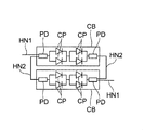
- FIG. 1D in the circuit configuration shown in FIG. 1D as an example of the present invention, two LED chips CP connected in parallel are further connected in series, and both ends thereof are connected to the pad PD. Two substrates CB are formed, and the circuit substrates CB are connected in series. With such a configuration, the wiring HN1 for driving voltage application and the wiring HN2 for connection between the circuit boards CB are connected to different pads PD, thereby reducing the pad area while reducing the pad area. The number is as small as four. Furthermore, since the light emission amount of the LED chip CP is constant at the average of each parallel portion, unevenness in illuminance can be suppressed. Further, if the required voltage of one LED chip CP is 6V, the driving voltage is 24V as a whole, so that the driving voltage can be suppressed lower than that of the configuration of FIG.
- two LED chips CP connected in parallel constitute a small group
- two LED chips CP connected in parallel further connected in series constitute a medium group.
- the present invention is not limited to the above example.
- three or more light emitting elements may be connected in parallel
- three or more small group light emitting elements may be connected in series in a circuit board.
- the light emitting element is not limited to the LED chip.
- a plurality of the circuit boards are provided, and by connecting the pads connected to the ends of the middle group for each circuit board, a large group is formed, and both ends of the large group are formed. It is preferable to connect to an external drive source through a pad.
- two LED chips CP connected in parallel are further connected in series, and both ends thereof are connected to the pad PD.
- a wiring HN1 for applying a driving voltage and a wiring HN2 for connecting the circuit boards CB are connected to different pads PD.
- the number of pads can be as small as four while the pad area is kept small.
- two circuit boards connected in series constitute a large group. Three or more circuit boards connected in series constituting a large group may be used.
- the circuit boards connected in series may be circuit boards of different series numbers.
- a thin lighting device while enabling light emission of two or more colors.
- a power receiving portion (pad) from an external drive power source mounted on the circuit board end ) Can be reduced (the anode and cathode lead locations of the light-emitting elements can be separated), and the pad mounting area can be reduced. Further, the number of pads can be reduced, the connecting portion can be made smaller, and the number of connecting wirings can be reduced.
- the distance between the circuit board and the light emitting element By setting the distance between the circuit board and the light emitting element to be small and using a light emitting element having a low height, it is possible to emit two or more colors and not emit light by ensuring the circuit board width. By thinning the edge, a lighting device having a large light emitting surface while being thin can be realized.
- a small group of light emitting elements connected in parallel can be further connected in series to form a middle group, so that the driving voltage can be set low while using more light emitting elements, and the safety is improved. Rise.
- the wiring distance can be shortened by arranging the middle groups connected in series next to each other.
- FIG. 2 is a diagram comparing a circuit board configuration of a comparative example and a circuit board configuration according to an example of the present invention, in which (a) is a diagram schematically illustrating a circuit board of a comparative example, and (b) is a circuit configuration of the comparative example.
- (C) is a figure which shows another circuit structure of a comparative example
- (d) is a figure which shows the circuit structure by an example of this invention. It is a figure which shows the circuit board structure concerning another comparative example. It is the figure cut
- FIG. 2 is a diagram illustrating a circuit configuration of a light source 2.
- FIG. It is a figure which shows the surface side (a) of the board
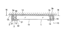
- FIG. 3 is a vertical sectional view of the lighting device 10.
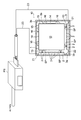
- FIG. 4 is a schematic diagram in which the configuration of FIG. 3 is cut along the VI-VI line and viewed in the direction of the arrow, and a drive voltage source of the light source is combined.
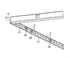
- FIG. 5 is a view of the light source with the light guide plate removed from the case.
- the illuminating device according to the present embodiment is an illuminating device 10 having an irradiation surface that emits surface light.
- the illuminating device is preferably attached to an indoor ceiling CL and used as indoor illumination.
- the illuminating device 10 includes a first main surface 11 that emits light and a second main surface 12 that faces the first main surface and extends substantially in parallel to the second main surface 12.
- a plurality of light emitting elements that extend in a direction intersecting the optical plate 1 and the first main surface 11 and the second main surface 12 and are opposed to one side surface portion that becomes the incident surface 13 of the light guide plate 1. 2, the light emitted from the light emitting element 2 is guided into the light guide plate 1 and emitted from the first main surface 11.
- the light guide plate 1 has a flat plate shape as shown in FIG. 3 and is configured to be integrally accommodated in the case 3 together with the light emitting element 2 so as to expose the first main surface 11.
- a lower plate 32 having a rectangular opening 31 is attached to support the light guide plate 1.
- the light emitting element 2 only needs to be a light source that emits illumination light in the direction of the incident surface 13.
- a plurality of point light sources (chip-type LEDs) disposed at intervals in the longitudinal direction of the incident surface 13. Can be used.
- an LED that emits white light with low power consumption and high emission intensity and an LED that emits light of a different color, such as orange.
- the LED 2 instead of the light emitting element 2, the LED 2 will be described below.
- the LEDs 2 are arranged in a plurality of lines in the longitudinal direction (direction perpendicular to the paper surface) of the substrate 21 attached to the inner side wall 3b of the case 3 with the emission colors alternately arranged at substantially equal intervals (for example, about 15 mm pitch). Has been.
- the LED 2 and the substrate 21 constitute a light source.
- the substrate 21 is, for example, about a full width in the longitudinal direction of the incident surface 13 and has a width of about 5 mm.
- a plurality of chip-type LEDs 2 are mounted on the substrate 21 at a predetermined pitch.
- substrate 21 is united in the longitudinal direction, it is good also as a structure which divides
- SP is a spacer that separates the substrate 21 and the light guide plate 1 from each other by a predetermined distance
- SC is a screw member that fixes the substrate 21 to the case 3.
- the substrate 21 is connected to the driving voltage source PS arranged outside the lighting device by the wiring 23, and the LED to which the voltage is applied is switched by a switching button (not shown), thereby the lighting device. The emission color can be switched.
- FIG. 6 is a diagram showing a circuit configuration of the light source 2.
- three white LEDs 2 (W) mounted on one substrate 21 (A) are connected in parallel, and this is a small group SG (W), and six small groups SG (W) are connected in series. These are connected to pads 21AW formed at both ends of the substrate 21 (A) as a middle group MG (W).
- three orange LEDs 2 (O) mounted on the same substrate 21 (A) are connected in parallel, and this is a small group SG (O), and six small groups SG (O) are arranged in series.
- this is connected to pads 21AO formed on both ends of the substrate 21 (A) as a middle group MG (O).
- three white LEDs 2 (W) mounted on another substrate 21 (B) are connected in parallel, and this is a small group SG (W), and six small groups SG (W) are arranged in series. Thus, this is connected to pads 21BW formed on both ends of the substrate 21 (A) as a middle group MG (W).
- three orange LEDs 2 (O) mounted on the same substrate 21 (A) are connected in parallel, and this is a small group SG (O), and six small groups SG (O) are arranged in series. Thus, this is connected to pads 21BO formed at both ends of the substrate 21 (B) as a middle group MG (O).
- One of the pads 21AW and 21AO of the substrate 21 (A) is connected to one of the pads 21BW and 21BO of the substrate 21 (B) by independent wirings 22 so that the middle groups MG (W) and MG ( O) are connected in series to form a large group BG.
- the other pads 21AW and 21AO of the substrates 21 (A) and 21 (B) are connected to the drive voltage source PS shown in FIG.
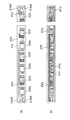
- FIG. 7 is a diagram showing the front side (a) and the back side (b) of the substrate 21A.
- white LEDs 2 (W) and orange LEDs 2 (O) are alternately arranged in a line along the longitudinal direction on the surface 21a of the substrate 21A.
- two pads 21AW and 21AO are arranged at both ends of the surface 21a of the substrate 21A in a direction perpendicular to the longitudinal direction of the substrate. According to this embodiment, since a single wiring is connected to any of the pads 21BW and 21BO, soldering can be easily performed even if the pad area is small.
- the conductive pattern PT1 formed on the surface 21a of the substrate 21A connects the pad 21AW on the left side with the anode side of the white LED 2 (W) in the drawing.
- the conductive pattern PT2 formed on the back surface 21b of the substrate 21A is connected to the right side pad 21AW in the drawing on the surface 21a of the substrate 21A through the cathode side of the white LED 2 (W) and vias penetrating the substrate 21A. is doing.
- the conductive pattern PT3 formed on the back surface 21b of the substrate 21A is connected to the pad 21AO on the right side in the drawing on the front surface 21a of the substrate 21A through a via penetrating the substrate 21A and the orange LED 2 (O). Connected to the anode side.
- the conductive pattern PT4 formed on the back surface 21b of the substrate 21A is connected to the cathode side of the orange LED 2 (O) through a via penetrating the substrate 21A, and further via a via penetrating the substrate 21A. It is connected to the pad 21AO on the right side in the figure on the surface 21a of 21A.
- three LEDs 2 (W) and 2 (O) connected in parallel are further connected in series, and two substrates 21A (21B) are connected to the pads 21AW and 21AO at both ends.
- the substrates 21A and 21B are connected in series.
- the wiring 23 for driving voltage application and the wiring 22 for connecting between the circuit boards 21A and 21B are connected to different pads, while the pad area is kept small, The number of pads is as small as four.
- the light emission amounts of the LEDs 2 (W) and 2 (O) are constant at the average of the parallel portions.
- the drive voltage can be kept low.
- an illumination device that is less likely to cause light unevenness, has a large light emission amount, is highly safe, and can emit light of a plurality of colors. That is, by connecting LED chips connected in parallel, it is possible to mount a larger number of LED chips, and the drive voltage value can be set low, and a large voltage is not required. Since cables can be used, costs can be reduced while ensuring safety. By arranging the groups of LEDs connected in series next to each other, even if there is a group that does not emit light, the area that does not emit light does not become too large, and light unevenness does not easily occur. In addition, by configuring a group of LEDs with a plurality of substrates, it becomes easier to mount more LEDs.
- the board connection part (wiring 22)
- the current is completely cut off, so that an excessive current does not flow and the safety is higher. It becomes composition.
- pads for power supply connection at both ends of a group of LEDs connected in series, it is possible to avoid the concentration of pads on one side, the number of pads on one side can be reduced, and the number of pads is also reduced. be able to.
- each group of LEDs connected in series with different emission colors, it is possible to emit light of two or more colors. In the case of two or more colors, the number of power supplies (wirings 23) increases, but the area of the pad and the board connecting portion can be minimized by the effect of the circuit configuration.
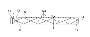
- FIG. 8 is a sectional view showing only the light source and the light guide plate. With reference to FIG. 8, operation
- movement of the illuminating device concerning this embodiment is demonstrated.
- Light emitted from the LED 2 and incident from the incident surface 13 of the light guide plate 1 is guided through the light guide plate 1 while being totally reflected.
- the light reaching the facing surface 14 is reflected here and guided in the opposite direction.
- the light incident on the diffusion dot 12a diffuses in various directions.
- the light diffused downward by the diffusing dots 12a is directed to the opposite lower surface (first main surface 11), and the light satisfying the total reflection condition continues to be guided in the light guide plate 1, but from the total reflection condition
- the detached light is emitted from the first main surface 11 to the outside and becomes illumination light.
- the light diffused upward by the diffusing dots 12 a is emitted from the second main surface 12, is reflected inside the upper case 3, enters the light guide plate 1 again, and is transmitted through the first main surface 11. And then injected outside.
- a plurality of the middle groups are provided on the same substrate with different emission colors of the light emitting elements.
- the number of pads can be reduced, so that in a lighting device having light emitting elements of different light emitting colors, thinning is not hindered even when light emission control of light emitting elements of different light emitting colors is performed independently.
- the light-emitting element is a chip-type LED, which irradiates light perpendicularly or parallel to the mounting surface of the substrate and faces the incident surface, which is a side end surface of the light guide plate, along the side end surface. It is preferable to line up in a row. Accordingly, the lighting device can be made thinner.
- the optical path deflecting unit may be a plurality of V-shaped or trapezoidal grooves provided in parallel to the substrate of the light emitting element on the second main surface.
- the light emission direction from the light emitting element mounted on the circuit board may be not only perpendicular to the mounting surface but also parallel.
Landscapes
- Planar Illumination Modules (AREA)
Abstract
省エネを図りつつも、十分な照度を確保でき、駆動電圧を低く抑えつつ、薄形を確保できる照明装置を提供する。並列に接続した2つのLEDチップCP同士を、更に直列に接続して、その両端をパッドPDに接続した回路基板CBを2つ形成し、この回路基板CBを直列に接続したものである。このような構成とすれば、駆動電圧印加用の配線HN1と、回路基板CB間の接続を行うための配線HN2とを別なパッドPDに接続することで、パッド面積を小さく抑えながらも、パッド数は4個と少なくて済む。更に、LEDチップCPの発光量が各並列部平均で一定となるから、照度ムラを抑えることができる。又、1つのLEDチップCPの必要な電圧が6Vであるとすると、全体で24Vの駆動電圧になるので、比較例の構成に比べて駆動電圧を低く抑えることができる。
Description
本発明は、照明装置に関し、例えば、住宅や店舗等の空間演出で使用される照明器具に用いられると好適な照明装置に関する。
板状導光板の端面に、線状または直線上に発光素子を配置し、端面である入射面から導光板内に発光素子からの光を入射し、導光板内を導光させ、入射端面と隣接し対向する2面のいずれかに光取り出し手段を設け、この光取り出し手段により導光板内を導光する光を少しずつ外部に射出し、結果として面状発光を行わせる、所謂、エッジライトタイプの照明装置が知られている。この導光板を用いたエッジライトタイプの照明装置は、液晶モニターのバックライトとして多く用いられてきたが、このようなバックライトを転用することで、薄形でデザイン性に優れた照明装置が提供できる。
又、省エネを図るべく、消費電力が小さいLEDチップを照明装置の光源として用いることが行われている。しかるに、1つのLEDチップの発光量は比較的小さいので、照明装置として十分な照度を確保する為に、複数のLEDチップを搭載することが行われている。しかるに、LEDチップの数を増大させようとすると、それに併せて駆動電圧も増大する可能性があるが、それによりコスト増を招くこととなる。
これに対し特許文献1では、電源回路で生成できる電圧で駆動できる数のLEDチップを直列に接続するとともに、このように直列接続した複数のLEDチップからなる2つのグループを構成し、これらの各グループに対して共通の電源回路から電力供給を行う面光源ユニットが開示されている。特許文献1の面光源ユニットによれば、複数のLEDチップを低駆動電圧で発光させることができる。又、少なくとも同一のグループに属する複数のLEDチップには同一の駆動電流が流れるので、LEDチップからの出射光量が一定であるから、導光板から出射される光に輝度ばらつきが発生しないという効果がある。更に、複数LEDチップの全てを直列に接続した場合と比較して低い駆動電圧で済むという利点もある。
ところで、上述したエッジライトタイプの照明装置は、非常に薄形であるので、導光板の側面に沿って発光素子を配置する面積が限られる。具体的には、照明装置の厚さに対して、発光素子の回路基板に許される幅は5mm程度である。このように細幅の回路基板に搭載する発光素子、例えばLEDチップは小型のものに限られるので、発光量が更に制限されるから、照明装置として必要な照度を確保するためには、LEDチップの数を相当に増やす必要があるが、駆動電圧は低いままとすることが望まれる。すると、各LEDチップを並列に配置する必要が生じ、それにより回路基板に設ける駆動電圧印加用のパッドの数を増やす必要が生じる。ここで、比較的大型の照明装置であれば、大型の回路基板を用いることができるので、パッド数を増やすことに特に障害がないが、エッジライトタイプの照明装置では、回路基板の面積が増大すると、薄型化が妨げられてしまうという問題がある。特に、近年の照明装置においては、単色のみならず、異なる色の照明光を出射することが望まれており、その場合、回路数が増えることとなり、パッド数の更なる増加を招くため、回路基板の面積の問題がより顕在化することになる。
本発明は、上記の事情に鑑みてなされたものであって、省エネを図りつつも、十分な照度を確保でき、駆動電圧を低く抑えつつ、薄形を確保できる照明装置を提供することを目的とする。
本発明による照明装置は、
光源と、
前記光源から出射された光を入射する入射面と、前記入射面から入射した光を出射する第1主面と、前記第1主面に対向し光路偏向手段を形成した第2主面とを有する導光板と、を有する照明装置において、
前記光源は、発光素子と、前記発光素子を実装した回路基板とを有し、
前記回路基板上において、複数の前記発光素子を並列に接続することによって形成した小グループを、複数個更に直列に接続して中グループを形成しており、前記中グループの両端を、前記発光素子を駆動するために外部より電圧を印加するパッドに接続してなることを特徴とする。
光源と、
前記光源から出射された光を入射する入射面と、前記入射面から入射した光を出射する第1主面と、前記第1主面に対向し光路偏向手段を形成した第2主面とを有する導光板と、を有する照明装置において、
前記光源は、発光素子と、前記発光素子を実装した回路基板とを有し、
前記回路基板上において、複数の前記発光素子を並列に接続することによって形成した小グループを、複数個更に直列に接続して中グループを形成しており、前記中グループの両端を、前記発光素子を駆動するために外部より電圧を印加するパッドに接続してなることを特徴とする。
本発明の効果について,図面を参照して説明する。図1(a)は、比較例の回路基板を模式的に示す図である。図1(a)においては、4つのLEDチップCPを直列に接続して、その両端をパッドPDに接続した回路基板CBを2つ、配線HN2により直列に接続した回路構成である。外部駆動源からの電圧は、配線HN1を介して2つの回路基板CBの端に設けたパッドPDに印加されるようになっている。図1(a)の回路構成の場合、駆動電圧を印加するパッドPDの数は比較的少なくて済むが、8つのLEDチップCPを直列に接続しているために、1つのLEDチップCPの必要な電圧が6Vであるとすると、全体で48Vの駆動電圧が必要になり、配線HN1のケーブル径を太くせざるを得ず、半田付けがしにくくなったり、高価な駆動源が必要になるなどの問題がある。
又、図1(b)に示す比較例の回路構成では、4つのLEDチップCPを直列に接続して、その両端をパッドPDに接続した回路基板CBを2つ形成し、配線HN2により並列に接続したものである。かかる回路構成の場合、1つのLEDチップCPの必要な電圧が6Vであるとすると、全体で24Vの駆動電圧になるので、図1(a)に示す回路構成に比べ、駆動電圧を大幅に低下させることができる。しかしながら、1つのパッドPDに、駆動電圧印加用の配線HN1と、回路基板CB間の接続を行うための配線HN2とを同時に接続しなくてはならないため、半田付けを行うためにパッドPDの面積を大きく確保する必要がある。
さもなくば、この回路構成を図1(c)に示すように変形し、駆動電圧印加用の配線HN1と、回路基板CB間の接続を行うための配線HN2とを、別のパッドPDに接続させることもできるが、かかる場合にはパッド数が8個となり、それにより回路基板の面積を増大させる必要が生じる。
これに対し、本発明の一例となる、図1(d)に示す回路構成では、並列に接続した2つのLEDチップCP同士を、更に直列に接続して、その両端をパッドPDに接続した回路基板CBを2つ形成し、この回路基板CBを直列に接続したものである。このような構成とすれば、駆動電圧印加用の配線HN1と、回路基板CB間の接続を行うための配線HN2とを別なパッドPDに接続することで、パッド面積を小さく抑えながらも、パッド数は4個と少なくて済む。更に、LEDチップCPの発光量が各並列部平均で一定となるから、照度ムラを抑えることができる。又、1つのLEDチップCPの必要な電圧が6Vであるとすると、全体で24Vの駆動電圧になるので、図1(a)の構成に比べて駆動電圧を低く抑えることができる。
ここで、並列に接続した2つのLEDチップCPが小グループを構成し、並列に接続した2つのLEDチップCPを更に直列に接続したものが中グループを構成する。尚、以上の例に限られず、小グループでは3個以上の発光素子を並列に接続して良く、回路基板内で小グループの発光素子を3つ以上直列に接続しても良い。発光素子とはLEDチップに限られない。
上記照明装置において、前記回路基板は複数個設けられ、前記回路基板毎に前記中グループの端部に接続した前記パッド同士を接続することで、大グループを形成し、前記大グループの両端を、パッドを介して外部駆動源に接続してなることが好ましい。
更に、図2に示す比較例の回路構成では、並列に接続した2つのLEDチップCP同士を、更に直列に接続して、その両端をパッドPDに接続した回路基板CBを2つ形成し、この回路基板CBを並列に接続したものである。かかる回路構成の場合、1つのLEDチップCPの必要な電圧が6Vであるとすると、全体で12Vの駆動電圧になるので、図1(b)に示す回路構成に比べ、駆動電圧を大幅に低下させることができる。しかしながら、1つのパッドPDに、駆動電圧印加用の配線HN1と、回路基板CB間の接続を行うための配線HN2とを同時に接続しなくてはならないため、パッドPDの面積を大きく確保する必要があるという,図1(b)の回路構成と同様な問題がある。
これに対し、図1(d)に示す回路構成を参照し、本発明によれば、並列に接続した2つのLEDチップCP同士を、更に直列に接続して、その両端をパッドPDに接続した回路基板CBを2つ形成し、この回路基板CBを直列に接続したので、駆動電圧印加用の配線HN1と、回路基板CB間の接続を行うための配線HN2とを別なパッドPDに接続することで、パッド面積を小さく抑えながらも、パッド数は4個と少なくて済む。尚、ここでは2つの回路基板を直列に接続したものが大グループを構成する。大グループを構成する直列に接続された回路基板は3つ以上でも良い。また、直列に接続される回路基板は、それぞれ違う直列数の回路基板でも良い。
本発明によれば、2色以上の発光を可能としながらも薄型の照明装置を提供可能にすることができる。2色以上の発光を可能とする照明装置を構成する際,複数枚の回路基板にわたって各色の発光素子を直列に接続することで,回路基板端に搭載する外部駆動電源からの給電受け部(パッド)の数を少なくし(発光素子のアノードとカソードの引き出し場所を別々にする)、パッドの搭載面積を小さくすることができる。また、パッド数も減り、連結部を小さくでき、連結用配線の本数を少なくできる。回路基板と発光素子との距離を小さく設定し、かつ高さの低い発光素子を使用したときでも、回路基板幅を確保することができるようにすることで、2色以上発光可能で、発光しない縁部を薄くすることで、薄型でありながら発光面の大きい照明装置が可能になる。特に、並列接続した発光素子同士の小グループを、更に直列に接続して中グループとすることで、より多くの発光素子を用いながらも、駆動電圧を低く設定することができ、より安全性が高まる。更に、直列で回路基板同士を接続して大グループを構成することにより,基板連結部が仮に切り離された場合には,電流は完全に遮断され、過大電流が流れるといった不具合を回避でき、更に安全性が高くなる。又、直列に接続された中グループ同士を隣り合って配置することで、配線距離を短くできる。
図3は、照明装置10の垂直方向断面図である。図4は、図3の構成をVI-VI線で切断して矢印方向に見た図と、光源の駆動電圧源とを組み合わせた模式図である。図5は、ケースから導光板を取り外した状態で光源を見た図である。本実施形態に係る照明装置は、面発光する照射面を備えた照明装置10であって、例えば、屋内の天井CL等に取り付けられて、屋内照明として用いられると好適である。この照明装置10は、図3に示すように、面発光する第1主面11、および、この第1主面に対向して略平行に延在する第2主面12を備える正方形状の導光板1と、第1主面11と第2主面12とに交差する方向に延在し該導光板1の入射面13となる一つの側面部に対向して配設される複数の発光素子2と、を備えて、発光素子2が射出する光を、導光板1内に導光して第1主面11から射出するものである。
導光板1は、図3に示すように平板状であって、第1主面11を露出するようにして、発光素子2と共にケース3に一体的に収容されて構成される。ケース3の下方には、導光板1を支持する為に、矩形開口31を有する下板32が取り付けられている。
発光素子2は、入射面13の方向に照明光を射出する光源であればよく、例えば、入射面13の長手方向に間隔をおいて配設する複数の点状光源(チップ型のLED)を用いることができる。また、低消費電力で発光強度が高く、白色発光するLEDと、それとは異なる色,例えばオレンジ色で発光するLEDを用いることが好ましい。ここで、発光素子2に代えてLED2として以後説明する。LED2は、ケース3の内側の側壁3bに取り付けられる基板21の長手方向(紙面に垂直な方向)に、直線的に略等間隔(例えば、約15mmピッチ)で、発光色を交互にして複数配列されている。LED2と基板21とで光源を構成する。
図5に示すように、基板21は、例えば、入射面13の長手方向の全幅程度の長さとされ、5mm程度の幅を有する。この基板21に複数のチップ型のLED2を所定ピッチで搭載する。このように、基板21は、長手方向に一体とされるが、複数の基板に分け、それぞれを電気的に接続する構成としてもよい。SPは、基板21と導光板1を所定距離隔てるスペーサであり、SCは、基板21をケース3に固定するねじ部材である。また、基板21は、図4に示すように、照明装置外部に配置される駆動電圧源PSと配線23により接続され、不図示の切り替えボタンにより、電圧を印加するLEDを切り替えることで、照明装置の発光色を切り替え可能である。
図6は、光源2の回路構成を示す図である。図6において、1つの基板21(A)上に実装された白色LED2(W)は3個ずつ並列に接続され、これを小グループSG(W)として、小グループSG(W)を6つ直列に配置してなり、これを中グループMG(W)として、基板21(A)の両端に形成したパッド21AWに接続している。又、同じ基板21(A)上に実装されたオレンジ色LED2(O)は3個ずつ並列に接続され、これを小グループSG(O)として、小グループSG(O)を6つ直列に配置してなり、これを中グループMG(O)として、基板21(A)の両端に形成したパッド21AOに接続している。
又、別の基板21(B)上に実装された白色LED2(W)は3個ずつ並列に接続され、これを小グループSG(W)として、小グループSG(W)を6つ直列に配置してなり、これを中グループMG(W)として、基板21(A)の両端に形成したパッド21BWに接続している。又、同じ基板21(A)上に実装されたオレンジ色LED2(O)は3個ずつ並列に接続され、これを小グループSG(O)として、小グループSG(O)を6つ直列に配置してなり、これを中グループMG(O)として、基板21(B)の両端に形成したパッド21BOに接続している。
基板21(A)の一方のパッド21AW,21AOは、それぞれ独立した配線22により基板21(B)の一方のパッド21BW,21BOと接続され、これにより、LEDの中グループMG(W),MG(O)は直列に接続されて大グループBGを構成する。尚、基板21(A)、21(B)の他方のパッド21AW,21AOは、それぞれ独立した配線23を介して図2に示す駆動電圧源PSに接続されている。
図7は、基板21Aの表面側(a)と、裏面側(b)とを示す図である。基板21Bも同様である。本実施形態では、基板21Aの表面21aには、白色LED2(W)とオレンジ色LED2(O)とが交互に、長手方向に沿って1列に並べて配置されている。更に、基板21Aの表面21aの両端には、それぞれ2つのパッド21AW,21AOが、基板長手方向に直交する方向に並べて配置されている。本実施形態によれば、いずれのパッド21BW,21BOにも単独の配線が結線されるので、パッド面積が小さくても、半田付けを容易に行うことができる。
基板21Aの表面21aに形成された導電パターンPT1は、図で左側のパッド21AWと、白色LED2(W)のアノード側とを接続している。一方、基板21Aの裏面21bに形成された導電パターンPT2は、白色LED2(W)のカソード側と、基板21Aを貫通するビアを介して、基板21Aの表面21aにおける図で右側のパッド21AWに接続している。
一方、基板21Aの裏面21bに形成された導電パターンPT3は、基板21Aを貫通するビアを介して、基板21Aの表面21aにおける図で右側のパッド21AOに接続するとともに、オレンジ色LED2(O)のアノード側とを接続している。一方、基板21Aの裏面21bに形成された導電パターンPT4は、基板21Aを貫通するビアを介してオレンジ色LED2(O)のカソード側に接続し、更に基板21Aを貫通するビアを介して、基板21Aの表面21aにおける図で右側のパッド21AOに接続している。
本実施形態によれば、並列に接続した3つのLED2(W),2(O)同士をそれぞれ、更に直列に接続して、その両端をパッド21AW,21AOに接続した基板21A(21B)を2つ形成し、この基板21A,21Bを直列に接続したものである。このような構成とすれば、駆動電圧印加用の配線23と、回路基板21A、21B間の接続を行うための配線22とを別なパッドに接続することで、パッド面積を小さく抑えながらも、パッド数は4個と少なくて済む。更に、LED2(W),2(O)の発光量が各並列部平均で一定となる。又、駆動電圧を低く抑えることができる。
本実施形態によれば、光ムラが起きにくく,発光量が大きく、安全性が高く,かつ複数色の発光が可能な照明装置を提供できる。すなわち、LEDチップを並列接続したものを直列に接続することにより,より多くのLEDチップを搭載可能としつつ,駆動電圧値を低く設定することができ、大電圧を必要としないため、比較的細いケーブル等を使用できるので、安全を確保しつつコストを低減できる。直列に接続されたLEDのグループ同士を隣り合って配置することで,発光していないグループがある状態でも,発光しないエリアが大きくなりすぎることがなく,光ムラが起きにくくなる。又、複数の基板でLEDのグループを構成することにより、よりLEDを多く搭載することが容易になる。更に、直列で回路基板同士を接続する構成により、基板連結部(配線22)が万が一切り離された場合は,電流は完全に遮断され,過大電流が流れるといった現象が起きず,より安全性が高い構成となる。さらに、直列接続されたLEDのグループの両端に電源接続用のパッドを設けることで,パッドが片側に集中することが回避され,片側のパッドの数を減らすことができ,かつパッド数も少なくすることができる。各直列接続したLEDのグループがそれぞれ異なる発光色で構成することにより,2色以上の発光が可能になる。2色以上の場合,電源供給本数(配線23)は増加するが,上記回路構成の効果により,パッドならびに基板連結部の面積は最小限で抑えられる。
図8は、光源と導光板のみを示す断面図である。図8を参照して、本実施形態にかかる照明装置の動作について説明する。LED2から出射して、導光板1の入射面13から入射した光は、全反射しながら導光板1内を導光する。対向面14に至った光は、ここで反射して逆方向に導光される。導光途中で、拡散ドット12aに入射した光は、種々の方向に拡散する。拡散ドット12aで下方に拡散された光は、対向する下面(第1主面11)に向かい、全反射条件を満足する光は、さらに導光板1内を導光し続けるが、全反射条件から外れた光は、第1主面11から外部へと射出され照明光となる。一方、拡散ドット12aで上方に拡散された光は、第2主面12から出射して、上側のケース3の内側で反射し、再び導光板1内に入射し、第1主面11を透過して外部へ射出される。
以下、好ましい態様についてまとめて説明する。
前記中グループは、前記発光素子の発光色を異ならせて同一基板上に複数個設けられていることが好ましい。本発明によればパッド数を少なく抑えることができるので、異なる発光色の発光素子を有する照明装置において、異なる発光色の発光素子を独立に発光制御する場合でも、薄型化を妨げることがない。
前記発光素子はチップ型のLEDであり、前記基板の実装面に対して垂直または平行に光を照射し,前記導光板の側端面である前記入射面に対向して当該側端面に沿って1列に並んでいることが好ましい。これにより照明装置をより薄形とできる。
本発明は、明細書に記載の実施態様に限定されるものではなく、他の実施態様・変形例を含むことは、本明細書に記載された実施態様や技術思想から本分野の当業者にとって明らかである。例えば、光路偏向手段は、第2主面において発光素子の基板に対して平行に設けたV字状又は台形状の複数の溝であっても良い。又、回路基板に実装された発光素子からの発光方向は、実装面に対して垂直のみならず、平行であっても良い。
1 導光板
2 発光素子(LEDチップ)、光源
3 ケース
3b 側壁
10 照明装置
11 第1主面(出射面)
12 第2主面
12a 拡散ドット
13 入射面
14 対向面
15 反射テープ
21A、21B 基板
21AO パッド
21AW パッド
21BO パッド
21BW パッド
21a 表面
21b 裏面
22 配線
23 配線
31 矩形開口
32 下板
CL 天井
PS 駆動電圧源
PT1 導電パターン
PT2 導電パターン
PT3 導電パターン
PT4 導電パターン
BG 大グループ
MG 中グループ
SG 小グループ
2 発光素子(LEDチップ)、光源
3 ケース
3b 側壁
10 照明装置
11 第1主面(出射面)
12 第2主面
12a 拡散ドット
13 入射面
14 対向面
15 反射テープ
21A、21B 基板
21AO パッド
21AW パッド
21BO パッド
21BW パッド
21a 表面
21b 裏面
22 配線
23 配線
31 矩形開口
32 下板
CL 天井
PS 駆動電圧源
PT1 導電パターン
PT2 導電パターン
PT3 導電パターン
PT4 導電パターン
BG 大グループ
MG 中グループ
SG 小グループ
Claims (4)
- 光源と、
前記光源から出射された光を入射する入射面と、前記入射面から入射した光を出射する第1主面と、前記第1主面に対向し光路偏向手段を形成した第2主面とを有する導光板と、を有する照明装置において、
前記光源は、発光素子と、前記発光素子を実装した回路基板とを有し、
前記回路基板上において、複数の前記発光素子を並列に接続することによって形成した小グループを、複数個更に直列に接続して中グループを形成しており、前記中グループの両端を、前記発光素子を駆動するために外部より電圧を印加するパッドに接続してなることを特徴とする照明装置。 - 前記回路基板は複数個設けられ、前記回路基板毎に前記中グループの端部に接続した前記パッド同士を接続することで、大グループを形成し、前記大グループの両端を、パッドを介して外部駆動源に接続してなることを特徴とする請求項1に記載の照明装置。
- 前記中グループは、前記発光素子の発光色を異ならせて同一基板上に複数個設けられていることを特徴とする請求項1又は2に記載の照明装置。
- 前記発光素子はチップ型のLEDであり、前記基板の実装面に対して垂直または平行に光を照射し,前記導光板の側端面である前記入射面に対向して当該側端面に沿って1列に並んでいることを特徴とする請求項1~3のいずれかに記載の照明装置。
Applications Claiming Priority (2)
| Application Number | Priority Date | Filing Date | Title |
|---|---|---|---|
| JP2013063923 | 2013-03-26 | ||
| JP2013-063923 | 2013-03-26 |
Publications (1)
| Publication Number | Publication Date |
|---|---|
| WO2014156440A1 true WO2014156440A1 (ja) | 2014-10-02 |
Family
ID=51623435
Family Applications (1)
| Application Number | Title | Priority Date | Filing Date |
|---|---|---|---|
| PCT/JP2014/054619 Ceased WO2014156440A1 (ja) | 2013-03-26 | 2014-02-26 | 照明装置 |
Country Status (1)
| Country | Link |
|---|---|
| WO (1) | WO2014156440A1 (ja) |
Cited By (1)
| Publication number | Priority date | Publication date | Assignee | Title |
|---|---|---|---|---|
| JP2021168255A (ja) * | 2020-04-10 | 2021-10-21 | コイズミ照明株式会社 | 電子装置 |
Citations (6)
| Publication number | Priority date | Publication date | Assignee | Title |
|---|---|---|---|---|
| JP2008041645A (ja) * | 2006-08-07 | 2008-02-21 | Samsung Electronics Co Ltd | バックライトユニット、バックライトユニットの製造方法、及びバックライトユニットを含む表示装置 |
| JP2008287892A (ja) * | 2007-05-15 | 2008-11-27 | Hitachi Ltd | 照明装置および該照明装置を用いた液晶表示装置 |
| WO2010013544A1 (ja) * | 2008-07-29 | 2010-02-04 | シャープ株式会社 | 照明装置、表示装置、及びテレビ受信装置 |
| JP2010282911A (ja) * | 2009-06-08 | 2010-12-16 | Victor Co Of Japan Ltd | バックライト装置および画像表示装置 |
| WO2011042999A1 (ja) * | 2009-10-07 | 2011-04-14 | シャープ株式会社 | 光源モジュール、及びそれを備えた電子機器 |
| JP2012155880A (ja) * | 2011-01-24 | 2012-08-16 | Panasonic Corp | 照明光源 |
-
2014
- 2014-02-26 WO PCT/JP2014/054619 patent/WO2014156440A1/ja not_active Ceased
Patent Citations (6)
| Publication number | Priority date | Publication date | Assignee | Title |
|---|---|---|---|---|
| JP2008041645A (ja) * | 2006-08-07 | 2008-02-21 | Samsung Electronics Co Ltd | バックライトユニット、バックライトユニットの製造方法、及びバックライトユニットを含む表示装置 |
| JP2008287892A (ja) * | 2007-05-15 | 2008-11-27 | Hitachi Ltd | 照明装置および該照明装置を用いた液晶表示装置 |
| WO2010013544A1 (ja) * | 2008-07-29 | 2010-02-04 | シャープ株式会社 | 照明装置、表示装置、及びテレビ受信装置 |
| JP2010282911A (ja) * | 2009-06-08 | 2010-12-16 | Victor Co Of Japan Ltd | バックライト装置および画像表示装置 |
| WO2011042999A1 (ja) * | 2009-10-07 | 2011-04-14 | シャープ株式会社 | 光源モジュール、及びそれを備えた電子機器 |
| JP2012155880A (ja) * | 2011-01-24 | 2012-08-16 | Panasonic Corp | 照明光源 |
Cited By (2)
| Publication number | Priority date | Publication date | Assignee | Title |
|---|---|---|---|---|
| JP2021168255A (ja) * | 2020-04-10 | 2021-10-21 | コイズミ照明株式会社 | 電子装置 |
| JP7428575B2 (ja) | 2020-04-10 | 2024-02-06 | コイズミ照明株式会社 | 電子装置 |
Similar Documents
| Publication | Publication Date | Title |
|---|---|---|
| JP4764928B2 (ja) | 端部コネクタを持つled照明ユニットおよびその組立品 | |
| JP4971706B2 (ja) | Ledを用いた面光源及びこれを備えるlcdバックライトユニット | |
| US10234112B2 (en) | Light source module and lighting device having same | |
| US20120014092A1 (en) | Backlight unit and display apparatus having the same | |
| CN103890488B (zh) | 发光模块 | |
| KR20070054825A (ko) | Led를 이용한 조명 장치 | |
| US11131885B2 (en) | Light emittng device | |
| JP2014120319A (ja) | 照明装置 | |
| CN102537733B (zh) | 发光模块及其制造方法 | |
| JP2011023295A (ja) | Led照明装置および画像表示装置 | |
| KR200468108Y1 (ko) | Led 패키지 모듈 및 이를 포함하는 조명장치 | |
| US20130083513A1 (en) | Light source unit, backlight unit, and flat panel display device | |
| JP5836812B2 (ja) | 線状光源装置、面発光装置、および液晶表示装置 | |
| EP2492898A2 (en) | Light Emitting Device | |
| JP2020057595A (ja) | 発光装置 | |
| KR20120061292A (ko) | 광원 장치, 백라이트 유닛 및 이를 포함하는 표시 장치 | |
| WO2014156440A1 (ja) | 照明装置 | |
| JP2009187874A (ja) | Led光源装置 | |
| US11982432B2 (en) | Light emitting module for spotlight and spotlight | |
| JP5453580B1 (ja) | 発光モジュール | |
| KR200387500Y1 (ko) | 광색 변화되는 광고판 | |
| JP2009081083A (ja) | バックライト装置 | |
| JP2024081279A (ja) | 照明器具 | |
| KR20150088487A (ko) | 직하형 평판모듈 | |
| KR102115919B1 (ko) | 조명 장치 |
Legal Events
| Date | Code | Title | Description |
|---|---|---|---|
| 121 | Ep: the epo has been informed by wipo that ep was designated in this application |
Ref document number: 14772904 Country of ref document: EP Kind code of ref document: A1 |
|
| 122 | Ep: pct application non-entry in european phase |
Ref document number: 14772904 Country of ref document: EP Kind code of ref document: A1 |
|
| NENP | Non-entry into the national phase |
Ref country code: JP |
|
| NENP | Non-entry into the national phase |
Ref country code: DE |