WO2014156233A1 - シリコン系細線光導波路の加工方法 - Google Patents
シリコン系細線光導波路の加工方法 Download PDFInfo
- Publication number
- WO2014156233A1 WO2014156233A1 PCT/JP2014/050909 JP2014050909W WO2014156233A1 WO 2014156233 A1 WO2014156233 A1 WO 2014156233A1 JP 2014050909 W JP2014050909 W JP 2014050909W WO 2014156233 A1 WO2014156233 A1 WO 2014156233A1
- Authority
- WO
- WIPO (PCT)
- Prior art keywords
- silicon
- optical waveguide
- thin
- based thin
- optical
- Prior art date
- Legal status (The legal status is an assumption and is not a legal conclusion. Google has not performed a legal analysis and makes no representation as to the accuracy of the status listed.)
- Ceased
Links
Images



Classifications
-
- G—PHYSICS
- G02—OPTICS
- G02B—OPTICAL ELEMENTS, SYSTEMS OR APPARATUS
- G02B6/00—Light guides; Structural details of arrangements comprising light guides and other optical elements, e.g. couplings
- G02B6/10—Light guides; Structural details of arrangements comprising light guides and other optical elements, e.g. couplings of the optical waveguide type
- G02B6/12—Light guides; Structural details of arrangements comprising light guides and other optical elements, e.g. couplings of the optical waveguide type of the integrated circuit kind
- G02B6/13—Integrated optical circuits characterised by the manufacturing method
-
- G—PHYSICS
- G02—OPTICS
- G02B—OPTICAL ELEMENTS, SYSTEMS OR APPARATUS
- G02B6/00—Light guides; Structural details of arrangements comprising light guides and other optical elements, e.g. couplings
- G02B6/10—Light guides; Structural details of arrangements comprising light guides and other optical elements, e.g. couplings of the optical waveguide type
- G02B6/12—Light guides; Structural details of arrangements comprising light guides and other optical elements, e.g. couplings of the optical waveguide type of the integrated circuit kind
- G02B6/122—Basic optical elements, e.g. light-guiding paths
- G02B6/125—Bends, branchings or intersections
-
- G—PHYSICS
- G02—OPTICS
- G02B—OPTICAL ELEMENTS, SYSTEMS OR APPARATUS
- G02B6/00—Light guides; Structural details of arrangements comprising light guides and other optical elements, e.g. couplings
- G02B6/02—Optical fibres with cladding with or without a coating
- G02B6/02395—Glass optical fibre with a protective coating, e.g. two layer polymer coating deposited directly on a silica cladding surface during fibre manufacture
-
- G—PHYSICS
- G02—OPTICS
- G02B—OPTICAL ELEMENTS, SYSTEMS OR APPARATUS
- G02B6/00—Light guides; Structural details of arrangements comprising light guides and other optical elements, e.g. couplings
- G02B6/10—Light guides; Structural details of arrangements comprising light guides and other optical elements, e.g. couplings of the optical waveguide type
- G02B6/12—Light guides; Structural details of arrangements comprising light guides and other optical elements, e.g. couplings of the optical waveguide type of the integrated circuit kind
- G02B6/122—Basic optical elements, e.g. light-guiding paths
- G02B6/1223—Basic optical elements, e.g. light-guiding paths high refractive index type, i.e. high-contrast waveguides
-
- G—PHYSICS
- G02—OPTICS
- G02B—OPTICAL ELEMENTS, SYSTEMS OR APPARATUS
- G02B6/00—Light guides; Structural details of arrangements comprising light guides and other optical elements, e.g. couplings
- G02B6/10—Light guides; Structural details of arrangements comprising light guides and other optical elements, e.g. couplings of the optical waveguide type
- G02B6/12—Light guides; Structural details of arrangements comprising light guides and other optical elements, e.g. couplings of the optical waveguide type of the integrated circuit kind
- G02B6/13—Integrated optical circuits characterised by the manufacturing method
- G02B6/132—Integrated optical circuits characterised by the manufacturing method by deposition of thin films
-
- G—PHYSICS
- G02—OPTICS
- G02B—OPTICAL ELEMENTS, SYSTEMS OR APPARATUS
- G02B6/00—Light guides; Structural details of arrangements comprising light guides and other optical elements, e.g. couplings
- G02B6/10—Light guides; Structural details of arrangements comprising light guides and other optical elements, e.g. couplings of the optical waveguide type
- G02B6/12—Light guides; Structural details of arrangements comprising light guides and other optical elements, e.g. couplings of the optical waveguide type of the integrated circuit kind
- G02B6/13—Integrated optical circuits characterised by the manufacturing method
- G02B6/134—Integrated optical circuits characterised by the manufacturing method by substitution by dopant atoms
- G02B6/1347—Integrated optical circuits characterised by the manufacturing method by substitution by dopant atoms using ion implantation
-
- G—PHYSICS
- G02—OPTICS
- G02B—OPTICAL ELEMENTS, SYSTEMS OR APPARATUS
- G02B6/00—Light guides; Structural details of arrangements comprising light guides and other optical elements, e.g. couplings
- G02B6/24—Coupling light guides
- G02B6/245—Removing protective coverings of light guides before coupling
-
- G—PHYSICS
- G02—OPTICS
- G02B—OPTICAL ELEMENTS, SYSTEMS OR APPARATUS
- G02B6/00—Light guides; Structural details of arrangements comprising light guides and other optical elements, e.g. couplings
- G02B6/10—Light guides; Structural details of arrangements comprising light guides and other optical elements, e.g. couplings of the optical waveguide type
- G02B6/12—Light guides; Structural details of arrangements comprising light guides and other optical elements, e.g. couplings of the optical waveguide type of the integrated circuit kind
- G02B2006/12083—Constructional arrangements
- G02B2006/12119—Bend
-
- G—PHYSICS
- G02—OPTICS
- G02B—OPTICAL ELEMENTS, SYSTEMS OR APPARATUS
- G02B6/00—Light guides; Structural details of arrangements comprising light guides and other optical elements, e.g. couplings
- G02B6/10—Light guides; Structural details of arrangements comprising light guides and other optical elements, e.g. couplings of the optical waveguide type
- G02B6/12—Light guides; Structural details of arrangements comprising light guides and other optical elements, e.g. couplings of the optical waveguide type of the integrated circuit kind
- G02B2006/12083—Constructional arrangements
- G02B2006/12121—Laser
-
- G—PHYSICS
- G02—OPTICS
- G02B—OPTICAL ELEMENTS, SYSTEMS OR APPARATUS
- G02B6/00—Light guides; Structural details of arrangements comprising light guides and other optical elements, e.g. couplings
- G02B6/10—Light guides; Structural details of arrangements comprising light guides and other optical elements, e.g. couplings of the optical waveguide type
- G02B6/12—Light guides; Structural details of arrangements comprising light guides and other optical elements, e.g. couplings of the optical waveguide type of the integrated circuit kind
- G02B2006/12083—Constructional arrangements
- G02B2006/12123—Diode
-
- G—PHYSICS
- G02—OPTICS
- G02B—OPTICAL ELEMENTS, SYSTEMS OR APPARATUS
- G02B6/00—Light guides; Structural details of arrangements comprising light guides and other optical elements, e.g. couplings
- G02B6/10—Light guides; Structural details of arrangements comprising light guides and other optical elements, e.g. couplings of the optical waveguide type
- G02B6/12—Light guides; Structural details of arrangements comprising light guides and other optical elements, e.g. couplings of the optical waveguide type of the integrated circuit kind
- G02B2006/12166—Manufacturing methods
- G02B2006/12176—Etching
-
- G—PHYSICS
- G02—OPTICS
- G02B—OPTICAL ELEMENTS, SYSTEMS OR APPARATUS
- G02B6/00—Light guides; Structural details of arrangements comprising light guides and other optical elements, e.g. couplings
- G02B6/24—Coupling light guides
- G02B6/42—Coupling light guides with opto-electronic elements
- G02B6/4201—Packages, e.g. shape, construction, internal or external details
- G02B6/4204—Packages, e.g. shape, construction, internal or external details the coupling comprising intermediate optical elements, e.g. lenses, holograms
- G02B6/4214—Packages, e.g. shape, construction, internal or external details the coupling comprising intermediate optical elements, e.g. lenses, holograms the intermediate optical element having redirecting reflective means, e.g. mirrors, prisms for deflecting the radiation from horizontal to down- or upward direction toward a device
Definitions
- the present invention relates to a method for processing a silicon-based fine wire optical waveguide in which the end portion of the silicon-based fine wire optical waveguide is three-dimensionally curved.
- an optical circuit whose main component is a silicon-based optical waveguide is formed in the same plane for reasons of the manufacturing process, and the input / output of light to the optical circuit is the same as the surface on which the optical circuit is formed.
- a spot size converter (SSC) in which the end of a thin wire optical waveguide is processed into a tapered shape or an inversely tapered shape is most commonly used, and various variations have been proposed (for example, non-patented).
- Document 1 Non-Patent Document 2
- first core material that increases the spot size of propagating light and further propagates light through a second core that covers the tip and is larger than the first core. And optically couple with fibers.
- the relationship of the refractive index is as follows: first core material> second core material> cladding material.
- these structures are formed on the same plane for reasons of the manufacturing process, and the input / output of light to / from the optical circuit using these SSCs is limited to the lateral direction.
- an optical circuit mainly composed of a silicon-based thin optical waveguide and other optical devices such as an optical fiber, a light source, and a light receiver, it is different from the plane in which the optical circuit is formed. Coupling from the direction, particularly from the vertical direction, has many technical advantages in that it enables inspection of a silicon-based thin-wire optical waveguide device at the wafer stage, and allows a light source and a light receiver to be mounted from the vertical direction.
- Non-patent Documents 3 and 4 A method of coupling an optical device such as an optical fiber from a slightly inclined direction is known (Non-patent Documents 3 and 4).
- Non-patent literature 5 the method of forming an oblique mirror in the front-end
- Non-patent Documents 6 and 7 a method has recently been reported in which a silicon-based thin optical waveguide itself is three-dimensionally curved and coupled to an optical fiber or an optical waveguide.
- the method in which the silicon-based optical waveguide itself is three-dimensionally curved is not limited by the wavelength band unlike the planar diffraction grating type coupler, and the optical waveguide end and the mirror in the mirror reflection type are not limited. This is an excellent method without the problem of increased coupling loss due to the space between them. If this method is used, for example, an optical circuit having a silicon-based thin-wire optical waveguide as a main component, an end portion of the silicon-based thin-wire optical waveguide is curved upward, and light is input / output from above. realizable.
- Non-Patent Document 3 A method of spontaneous bending using a difference in stress (Non-Patent Document 3) is known.
- the method of three-dimensionally bending the silicon-based fine wire optical waveguide itself is an excellent method for coupling light in a direction different from the plane in which the silicon-based fine wire optical waveguide is formed.
- a silicon oxide film is formed on the upper part of the silicon-based thin optical waveguide by plasma CVD, and spontaneously using the difference in residual stress with the silicon oxide film formed by thermal oxidation of the base of the silicon-based thin optical waveguide.
- the method of bending has the following problems. (1) It is necessary to dry-etch a cantilever structure in which a silicon oxide film formed by plasma CVD and a silicon oxide film formed by plasma CVD and a thermally oxidized silicon oxide film are sandwiched between the upper and lower sides of a silicon-based thin optical waveguide.
- a high temperature heating process is required to obtain a large amount of bending, and an optical circuit formed on a substrate provided with metal wiring and a metal wiring for driving an active optical element are included on the same substrate. Like an optical circuit, it cannot be applied to an optical circuit in which components are destroyed by high-temperature processing. In addition, the process cost increases.
- the most ideal configuration of the three-dimensional bending waveguide is that the SSC exceeds the specifications of the planar diffraction grating type coupler except that optical coupling from above and below is impossible. It is considered that the entire core is bent three-dimensionally, or the tip portion of the SSC structure described above is three-dimensionally bent, but not only the first core material but also the second core material and the third core. In principle, it is impossible in Non-Patent Document 5 to bend a structure in which a material, a clad material, or the like is complicatedly combined.
- FIGS. (1) As shown in FIG. 6A and a side view thereof, a silicon layer on a silicon oxide film that is formed on a silicon substrate 1 that is an optical circuit substrate and serves as a support layer 2 is formed by lithography technology. To form a silicon-based fine wire optical waveguide 3. (2) Next, as shown in FIG. 6 (C), the end 4 of the silicon-based thin optical waveguide 3 formed by removing a part of the support layer 2 forms a silicon-based thin optical waveguide. A structure extending in a free space in the form of a cantilever from a planar end is formed.
- the entire surface of the silicon substrate 1 having the cantilever structure is irradiated with an ion beam from a specific direction above the substrate as shown in FIG. 6D, and as shown in FIG.
- the end portion 4 of the silicon-based fine wire optical waveguide having a cantilever structure is curved upward.
- JP 2013-178333 A Japanese Patent Application No. 2012-413164
- the present invention improves the conventional processing method of a silicon-based thin optical waveguide, reduces the light propagation loss of the silicon-based thin optical waveguide due to high-energy ion irradiation, and is a self-aligned and three-dimensionally curved silicon-based thin wire It is an object of the present invention to provide a method for processing a silicon-based thin-wire optical waveguide that can obtain the end of the optical waveguide.
- Means for solving the above problems are as follows. (1) A step of preparing an optical circuit substrate on which a plurality of silicon-based fine wire optical waveguides are formed via a support layer, and a desired silicon-based thin wire optical waveguide having an end portion among the silicon-based thin wire optical waveguides, Removing the support layer below the end of the silicon-based thin-line optical waveguide, and selectively forming a protective film on the silicon-based thin-line optical waveguide excluding the end of the silicon-based thin-line optical waveguide And a step of bending the end of the silicon-based fine wire optical waveguide in a self-aligned manner in the specific direction by implanting ions from the specific direction into the silicon-based fine wire optical waveguide.
- Optical waveguide processing method Optical waveguide processing method.
- (6) The method for processing a silicon-based fine wire optical waveguide according to (5), further comprising a step of installing an optical device at the curved end portion.
- (7) The method for processing a silicon-based thin optical waveguide according to (6), wherein the optical device is an optical fiber.
- (8) The method for processing a silicon-based thin optical waveguide according to (6), wherein the optical device is a photodetector.
- the protective film is made of a material having a heavy mass, and a step of forming a low refractive index material layer on the optical circuit substrate so that a terminal portion of the curved silicon-based thin optical waveguide is embedded.
- the silicon fine wire optical waveguide excluding at least all or part of the end of the silicon fine wire optical waveguide is protected from the intrusion of ions by the protective film, the light propagation of the silicon fine wire optical waveguide Loss is greatly reduced.
- a protective film 14 is formed on the upper part of the silicon-based fine-wire optical waveguide 13.
- the protective film 14 for example, a SiO 2 film formed to a thickness of 500 nm to 600 nm by the CVD method is used.
- the end portion 15 of the silicon-based fine wire optical waveguide 13 formed by removing the protective film 14 above the end portion 15 of the thin wire optical waveguide 13 is cantilevered from the planar end forming the optical waveguide in free space. To form a structure extending to the surface.
- a silicon substrate 11 having a cantilever structure is irradiated with an ion beam from a specific orientation above the substrate as shown in FIG. 1 (F), and as shown in FIG. Curve up the entire cantilever structure.
- ion beam irradiation conditions ion species, acceleration voltage, and dose
- the degree of bending can be reduced.
- any of those capable of bending a silicon-based thin optical waveguide can be used, but silicon ions, phosphorus ions, boron ions, and arsenic ions are preferable.
- silicon ions are not normally used in the CMOS process, silicon ions, which are the same element type as the material of the thin optical waveguide, are implanted, so that there is an advantage that alteration of the optical waveguide material itself can be suppressed.
- Phosphorus ions, boron ions, and arsenic ions are frequently used for ion implantation in CMOS processes, and have good compatibility with existing CMOS processes.
- the accelerating voltage of the ion beam is selected to be an appropriate value according to the thickness of the silicon-based thin wire optical waveguide and the ion species used.
- irradiation ions and atoms constituting the optical waveguide are formed in a region shallower than the depth of 50% from the surface with respect to the thickness of the silicon-based thin optical waveguide.
- the accelerating voltage may be adjusted so as to satisfy the condition for causing the collision phenomenon.
- the atomic density decreases instantaneously, a difference in density of the atomic density occurs between the irradiated region and the non-irradiated region, the sparse region shrinks, and the dense region expands, The force that equalizes the density difference becomes the force for bending. Therefore, when ion irradiation is performed by selecting an acceleration voltage condition in which the front surface side of the silicon-based thin-wire optical waveguide is sparse and the back surface side is dense, it is curved upward.
- the upper limit of the optimum acceleration energy when a silicon-based thin optical waveguide having a thickness of 150 nm to 250 nm is bent using silicon ions is preferably 80 keV to 130 keV.
- silicon ions are irradiated at an acceleration voltage of 80 keV to 130 keV or more, a collision phenomenon occurs in a region deeper than 50% from the surface, so that the stress to bend upward and the stress to bend downward are antagonistic. As a result, it is impossible to bend upward.
- the acceleration voltage of silicon ions is 30 keV to 50 keV or less, it can generate an upward bending force only in a small area on the surface. It becomes difficult to bend it.
- the upper limit of the optimum acceleration energy when a silicon-based thin optical waveguide having a thickness of 200 nm to 250 nm is bent using silicon ions is 100 keV to 110 keV.
- silicon ions are irradiated at an accelerating voltage of 100 keV to 110 keV or more, for the same reason as described above, the stress to bend upward and the stress to bend downward are antagonized, resulting in bending upward. This is because it becomes impossible.
- the lower limit of the optimum acceleration voltage is 40 keV to 45 keV. For the same reason as described above, it is difficult to bend greatly upward unless irradiation is performed with a very large dose.
- an acceleration voltage of 40 keV to 100 keV, more preferably an acceleration voltage of 60 keV to 90 keV, particularly about 80 keV is optimal for a 200 nm-thick silicon-based optical waveguide.
- an acceleration voltage between 40 keV and 110 keV, preferably an acceleration voltage between 60 keV and 100 keV, particularly around 90 keV is the optimum value.
- an acceleration voltage of 60 keV to 130 keV, preferably an acceleration voltage of 80 keV to 120 keV, particularly around 110 keV is the optimum value.
- the optimum accelerating voltage is determined by the distribution shape taken in the depth direction of the optical waveguide because the region where the ion-atom collision phenomenon occurs is the density of the film constituting the optical waveguide. This parameter also depends on the conditions, and varies depending on the film forming conditions of the film constituting the optical waveguide.
- the ion beam dose (number of ions irradiated per unit area) is a parameter that depends mainly on the length of the silicon-based optical waveguide that is desired to be curved upward, and almost depends on the width of the silicon-based optical waveguide. do not do. If the desired structure is a structure in which the end of the silicon-based thin-wire optical waveguide faces directly above the substrate, the longer the silicon-based thin-wire optical waveguide, the smaller the required dose, and the shorter, the more the dose. Necessary. However, in order to determine a dose for obtaining a desired shape, it is necessary to first determine an acceleration voltage for bending most efficiently. As shown in the examples described later, in the inventors' experiments, the optimal dose is on the order of 10 15 cm ⁇ 2 . The acceleration voltage and dose shown here are examples, and the appropriate acceleration voltage and dose can be adjusted according to the thickness of the waveguide.
- the curved portion is easily damaged by an external impact or the like, and it is not easy to mount another optical device.
- the periphery of the silicon-based thin-wire optical waveguide including the end portion 16 of the curved silicon-based thin-wire optical waveguide may be embedded with a low-refractive-index material layer 17 such as resin or glass for protection and reinforcement.
- the protective film 14 functions as a clad of a silicon-based thin optical waveguide, such as a SiO 2 film, it can be used as it is, but it can be used as it is. In this case, it is necessary to remove the low refractive index material layer 17 such as resin or glass before embedding.
- a silicon nitride film is formed around the end portion 16 by, for example, CVD after the step of FIG. And can be used as the second core material.
- the thickness of the protective film 14 in the first embodiment is selected so that irradiation ions do not penetrate the protective film.
- the protective film is, for example, SiO 2
- the silicon-based thin optical waveguide 13 except the end 15 of the silicon-based thin optical waveguide 13 is protected from the intrusion of ions by the protective film. The light propagation loss is greatly reduced.
- an optical device 18 such as a photodetector or an optical fiber in the bending and extending direction of the silicon-based thin optical waveguide.
- the optical signal can be coupled between the silicon-based fine wire optical waveguide and the optical device.
- the light receiver can receive the light output from the silicon-based thin optical waveguide, and when the optical device is a light source device such as a semiconductor laser, the light source Light output from the device can be input to the silicon-based fine wire optical waveguide.
- the optical device 18 is an optical fiber, the light output from the optical fiber side can be input to the silicon-based thin optical waveguide, and conversely, the light output from the silicon-based thin optical waveguide can be input to the optical fiber.
- FIGS. 2A and its side view (B) the steps (E) to (H) are substantially the same as those in the first embodiment, and detailed description thereof will be omitted.
- the support layer below the end 15 of the silicon-based thin-wire optical waveguide 13 12 is removed to form a cantilever structure.
- a protective film 14 is formed around the cantilever structure and on the silicon-based thin optical waveguide 13 by, for example, a CVD method.
- the silicon substrate 11 having the cantilever structure is irradiated with an ion beam from a specific direction above the substrate as shown in FIG. 2E, and the cantilever is cantilevered as shown in FIG. Curve upward over the entire beam structure.
- the curved portion is easily damaged by an external impact or the like, and it is not easy to mount another optical device, so as shown in FIG. 2 (G).
- the periphery of the silicon-based fine wire optical waveguide including the end portion 16 of the curved silicon-based thin wire optical waveguide may be embedded with a low refractive index material layer 17 such as a resin or glass for protection and reinforcement.
- the protective film 14 functions as a clad of a silicon-based thin optical waveguide, such as a SiO 2 film, it can be used as it is, but it can be used as it is. In this case, it is necessary to remove the low refractive index material layer 17 such as resin or glass before embedding.
- an optical signal can be coupled between the silicon-based thin-line optical waveguide and the optical device.
- the thickness of the protective film 14 in the second embodiment is too thick, the required irradiation energy becomes high, and a high energy ion implantation apparatus is essential. For this reason, it is practical to perform ion implantation at low energy by allowing the protective film to be thin and allowing ions to penetrate to some extent.
- the third embodiment is a modification of the first and second embodiments. 3A to 3E are substantially the same as those in the first embodiment, and detailed description thereof is omitted.
- the first is formed on the periphery of the cantilever structure and on the silicon-based thin optical waveguide 13 by, for example, the CVD method. Two protective films 19 are formed.
- the silicon substrate 11 having the cantilever structure is irradiated with an ion beam from a specific direction above the substrate as shown in FIG. 3 (G). As shown in FIG. The end 15 of the optical waveguide 13 is curved.
- the thickness of the second protective film 19 in the third embodiment is selected so that irradiation ions do not penetrate the protective film.
- the second protective film 19 is, for example, SiO 2 in a silicon-based thin optical waveguide having a thickness of 220 nm to 250 nm, it is sufficient that the thickness of the second protective film 19 is 500 nm or more.
- the curved portion is easily damaged by an external impact or the like, and it is not easy to mount another optical device.
- the periphery of the silicon-based fine wire optical waveguide including the end portion 16 of the curved silicon-based fine wire optical waveguide may be embedded with a low refractive index material layer such as resin or glass for protection and reinforcement.
- the protective film 14 and the second protective film 19 function as a clad of a silicon-based thin optical waveguide, such as a SiO 2 film, they can be used as they are without being removed. 14.
- the second protective film 19 is made of a material having a heavy mass such as metal, it is necessary to remove the second protective film 19 before embedding a low refractive index material layer such as resin or glass.
- an optical device such as a photodetector or an optical fiber is installed in the bending and extending direction of the silicon-based thin optical waveguide.
- an optical signal can be coupled between the silicon-based thin wire optical waveguide and the optical device.
- FIGS. 4A to 4D and steps of (F) to (I) are substantially the same as those of the second embodiment, and thus detailed description thereof is omitted.
- the fourth embodiment following the steps shown in FIGS. 4A to 4D, as shown in FIG. 4E, the top of the end portion 15 of the silicon-based thin-wire optical waveguide 13 having a cantilever structure is formed. A part of the protective film 14 is removed.
- the silicon substrate 11 having the cantilever structure is irradiated with an ion beam from a specific direction above the substrate as shown in FIG. 4 (F). As shown in FIG. A part of the end 15 of the optical waveguide 13 is curved.
- the thickness of the protective film 14 in the fourth embodiment is selected so that the irradiation ions do not penetrate the protective film.
- the protective film is, for example, SiO 2 , it is sufficient that the protective film has a thickness of 500 nm or more.
- the curved portion is easily damaged by an external impact or the like, and it is not easy to mount another optical device.
- the periphery of the silicon-based fine wire optical waveguide including the end portion 16 of the curved silicon-based thin wire optical waveguide may be embedded with a low refractive index material layer 17 such as a resin or glass for protection and reinforcement.
- the protective film 14 functions as a clad of a silicon-based thin optical waveguide, such as a SiO 2 film, it can be used as it is, but it can be used as it is. In this case, it is necessary to remove the low refractive index material layer 17 such as resin or glass before embedding.
- an optical signal can be coupled between the silicon-based thin optical waveguide and the optical device.
- the fourth embodiment has the following advantages when compared with the first to third embodiments. (1) It is possible to form a curved portion that is steeper than that of the first to third embodiments. (2) Since ions can be effectively implanted into the absence of the protective film, the curved portion can be formed at a lower dose than those of the second and third embodiments. (3) Since a protective film is also formed on a part of the end portion of the thin optical waveguide, the light propagation loss is smaller than that of the first embodiment.
- the silicon-based material used for the core structure of the thin-line optical waveguide in the present invention is not limited to crystalline silicon but may be amorphous silicon.
- amorphous silicon hydrogenated amorphous silicon is desirable in order to reduce the absorption loss of the material, but a material in which carbon, germanium or the like is added in addition to the silicon element may be used.
- silicon oxide, silicon nitride, silicon nitride oxide, or the like used as the second core material by covering the first core material such as crystalline silicon is used. Even if it is a silicon compound, the effect similar to having described in said each embodiment is acquired.
Landscapes
- Physics & Mathematics (AREA)
- General Physics & Mathematics (AREA)
- Optics & Photonics (AREA)
- Engineering & Computer Science (AREA)
- Microelectronics & Electronic Packaging (AREA)
- Optical Integrated Circuits (AREA)
- Optical Couplings Of Light Guides (AREA)
Abstract
Description
シリコン系コア材料と石英系クラッド材料の間で大きな比屈折率差が得られるために、小さな曲率半径で光導波路を曲げても光が放射損失することがなく、光回路の著しい小型化が実現できるためである。またシリコンCMOSLSIの製造プロセスの転用が可能なため、量産による低廉な製造コストが期待されている。
例えば、細線光導波路の端部をテーパー形状や逆テーパー形状に加工したスポットサイズ変換器(Spot Size Convertor:SSC)が最も一般的に利用され、様々なバリエーションが提案されている(例えば、非特許文献1、非特許文献2)。これらの原理は、テーパーや逆テーパー形状をした第一コア材料で、伝搬光のスポットサイズを大きくし、さらに先端部分を被覆しておりサイズが第一コアよりも大きい第二コアを光伝搬してファイバなどと光結合させる。ちなみに、屈折率の関係は、第一コア材>第二コア材>クラッド材となっている。しかし、これらの構造は作製プロセス上の理由から同一平面に形成され、これらのSSCを利用した光回路への光の入出力は真横の方向に限定される。
ところが、シリコン系細線光導波路を主要構成部とする光回路と光ファイバー・光源・受光器などの他の光デバイスとの光の入出力においては、光回路の形成されている平面内とは別の方向、特に垂直方向から結合できると、ウェハ段階でのシリコン系細線光導波路デバイスの検査が可能となったり、光源や受光器が垂直方向から実装できるなどの点で技術上多くの利点がある。
また、リブ型光導波路ではあるが、光導波路の端部の先端に斜めミラーを形成して光を上方に反射させる方法が報告されている(非特許文献5)。さらに、シリコン系細線光導波路自体を上方に立体的に湾曲させて光ファイバーや光導波路と結合させる方法が近年報告されている(非特許文献6、非特許文献7)。
特に実際上は、金属配線を施した回路基板上に形成された光回路や、能動光素子を駆動するための金属配線を同一基板上に含む光回路基板のように、高温処理を施すと構成要素が破壊されてしまうような光回路に適用可能な加工技術の開発が必要である。
しかし、シリコン系細線光導波路の上部にプラズマCVDでシリコン酸化膜を形成し、シリコン系細線光導波路の下地の熱酸化で形成されたシリコン酸化膜との残留応力の差を利用して自発的に湾曲させる方法には次のような問題点がある。
(1)シリコン系細線光導波路の上下をプラズマCVDで形成したシリコン酸化膜及び熱酸化シリコン酸化膜で挟み込んだ片持ち梁構造をドライエッチングで形成する必要があり、厚いシリコン酸化膜を深堀りした後に、さらに片持ち梁構造の酸化膜の下のシリコン基板の上部をくり抜くという複雑な加工プロセスが必要である。
(2)残留応力の差を利用するという原理に基づくため、湾曲曲率が片持ち梁構造全域で一定となり、湾曲曲率を局所的に変化させることは困難である。
(3)湾曲部の先端を任意の方位に向けるためには、片持ち梁の長さや上下の酸化膜層の厚さ及び加熱温度等を厳密に制御する必要があり、高い加工精度が要求される。
(4)上下の酸化膜の残留応力差を利用するため、上下の酸化膜を同じ成膜方法で形成した場合には湾曲させるのが困難である。
(5)大きな湾曲量を得るためには高温加熱プロセスが必要であり、金属配線を施した基板上に形成された光回路や、能動光素子を駆動するための金属配線を同一基板上に含む光回路のように、構成要素が高温処理で破壊されてしまう光回路への適用が不可能である。また、プロセスコストの増大を伴う。
(6)加えて、最も理想的な立体曲げ導波路の構成は、SSCは上下方向からの光結合が不可能である以外では平面回折格子型結合器のスペックを上回るため、前述したSSCの構造の全体を立体的に曲げ加工すること、あるいは前述したSSC構造の先端部分を立体的に曲げ加工することであると考えられるが、第一コア材のみならず、第二コア材、第三コア材、クラッド材などが複雑に組み合わさった構造を曲げ加工することは原理上、非特許文献5では不可能である。
(1)図6(A)及びその側面図(B)に示すように、光回路基板であるシリコン基板1の上に形成され支持層2となるシリコン酸化膜の上のシリコン層を、リソグラフィ技術を用いて加工し、シリコン系細線光導波路3を形成する。
(2)次に、図6(C)に示すように、支持層2の一部を除去することにより形成されたシリコン系細線光導波路3の端部4が、シリコン系細線光導波路を形成する平面端から片持ち梁状に自由空間中に伸長している構造を形成する。
(3)次に、片持ち梁構造を形成したシリコン基板1の全面に、図6(D)に示すように基板上方の特定の方位よりイオンビームを照射し、図6(E)に示すように、片持ち梁構造のシリコン系細線光導波路の端部4を上方向に湾曲させる。
(1)シリコン細線自体の内部ひずみ応力を利用しているため、上下の酸化膜が不要である。
(2)イオンビームの打ち込み方向や照射量を調節することにより、湾曲曲率を調節できる。
(3)曲率半径5μm以下の急峻な湾曲も可能である。したがって、素子を小型化できる。
(4)イオン打ち込み方向にセルフアライメント的に湾曲端部を伸長させることができる。
(5)低温プロセスで加工可能であり、高温処理で破壊されてしまう光回路への適用が可能となる。
(6)従来型のSSCを曲げ加工して上下から光結合を実現することが可能である。さらには、第一コア材だけを曲げ加工すれば、その後の工程で先端部分に第二コア材を形成してSSCを構成することも可能である。
このため、量産性の高い加工方法が実現できるという作用効果が得られる。
(1)支持層を介して複数のシリコン系細線光導波路が形成された光回路基板を用意する工程と、シリコン系細線光導波路のうち端部を有する所望のシリコン系細線光導波路に対して、該シリコン系細線光導波路の端部の下の支持層を除去する工程と、該シリコン系細線光導波路の端部を除いた該シリコン系細線光導波路の上に保護膜を選択的に形成する工程と、該シリコン系細線光導波路に対して特定の方向からイオンを打ち込むことにより、該特定の方向にセルフアライメント的に該シリコン系細線光導波路の端部を湾曲させる工程とを備えたシリコン系細線光導波路の加工方法。
(2)支持層を介して複数のシリコン系細線光導波路が形成された光回路基板を用意する工程と、シリコン系細線光導波路のうち端部を有する所望のシリコン系細線光導波路に対して、該シリコン系細線光導波路の端部の下の支持層を除去する工程と、該シリコン系細線光導波路の端部を含む該シリコン系細線光導波路の上に保護膜を形成する工程と、該シリコン系細線光導波路に対して特定の方向からイオンを打ち込むことにより、該特定の方向にセルフアライメント的に該シリコン系細線光導波路の端部を湾曲させる工程とを備えたシリコン系細線光導波路の加工方法。
(3)支持層を介して複数のシリコン系細線光導波路が形成された光回路基板を用意する工程と、シリコン系細線光導波路のうち端部を有する所望のシリコン系細線光導波路に対して、該シリコン系細線光導波路の端部の下の支持層を除去する工程と、該シリコン系細線光導波路の端部を除いた該シリコン系細線光導波路の上に保護膜を選択的に形成する工程と、該シリコン系細線光導波路の端部の上及び該保護膜の上に第2の保護膜を形成する工程と、該シリコン系細線光導波路に対して特定の方向からイオンを打ち込むことにより、該特定の方向にセルフアライメント的に該シリコン系細線光導波路の端部を湾曲させる工程とを備えたシリコン系細線光導波路の加工方法。
(4)支持層を介して複数のシリコン系細線光導波路が形成された光回路基板を用意する工程と、シリコン系細線光導波路のうち端部を有する所望のシリコン系細線光導波路に対して、該シリコン系細線光導波路の端部の下の支持層を除去する工程と、該シリコン系細線光導波路の端部を含む該シリコン系細線光導波路の上に保護膜を形成する工程と、該該シリコン系細線光導波路の端部の上の保護膜の一部を選択的に除去する工程と、該シリコン系細線光導波路に対して特定の方向からイオンを打ち込むことにより、該特定の方向にセルフアライメント的に該シリコン系細線光導波路の端部の一部を湾曲させる工程とを備えたシリコン系細線光導波路の加工方法。
(5)さらに、湾曲された該シリコン系細線光導波路の末端部が埋設されるように、上記光回路基板上に低屈折率材料層を形成する工程とを備えた(1)ないし(4)のいずれかに記載のシリコン系細線光導波路の加工方法。
(6)湾曲した上記末端部に光デバイスを設置する工程をさらに備えた(5)に記載のシリコン系細線光導波路の加工方法。
(7)上記光デバイスは、光ファイバーであることを特徴とする(6)に記載のシリコン系細線光導波路の加工方法。
(8)上記光デバイスは、フォトディテクターであることを特徴とする(6)に記載のシリコン系細線光導波路の加工方法。
(9)上記イオンは、Siイオンであることを特徴とする(1)ないし(8)のいずれかに記載のシリコン系細線光導波路の加工方法。
(10)上記保護膜は、シリコン系細線光導波路のクラッドとして機能することを特徴とする(1)ないし(5)のいずれかに記載のシリコン系細線光導波路の加工方法。
(11)上記保護膜は、質量が重い材料からなり、上記湾曲された該シリコン系細線光導波路の末端部が埋設されるように、上記光回路基板上に低屈折率材料層を形成する工程の前に除去されることを特徴とする(5)に記載のシリコン系細線光導波路の加工方法。
しかも、セルフアライメント的かつ立体的に湾曲したシリコン系細線光導波路の端部を得ることができる。
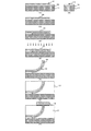
以下、図1(A)~(I)を用いて、本発明に係るシリコン系細線光導波路の加工方法を詳細に説明する。
(1)図1(A)及びその側面図(B)に示すように、光回路基板であるシリコン基板11の上に支持層12となる、例えば厚さ3μmの熱酸化シリコン膜を形成した後に、熱酸化シリコン膜の上に200nm~250nmの厚さにシリコン層を形成し、リソグラフィ技術を用いて加工し、幅400nm~1000nmのシリコン系細線光導波路13を形成する。
(2)次に、図1(C)及びその側面図(D)に示すように、シリコン系細線光導波路13の上部に保護膜14を形成する。保護膜14は、例えばSiO2膜をCVD法により500nm~600nmの厚さに形成したものを用いる。
(3)次に、図1(E)に示すように、ウェットエッチングやドライエッチングによりシリコン系細線光導波路13の端部15の下部のシリコン酸化膜等からなる支持層12の一部とシリコン系細線光導波路13の端部15の上部の保護膜14を除去することにより形成されたシリコン系細線光導波路13の端部15が、光導波路を形成する平面端から片持ち梁状に自由空間中に伸長している構造を形成する。
特に、シリコンイオンは、通常CMOSプロセスでは用いられないが、細線光導波路の材料と同一の元素種であるシリコンイオンを打ち込むため、光導波路材料自体の変質を抑制できるという利点がある。
また、リンイオン・ホウ素イオン・ヒ素イオンは、CMOSプロセスのイオン打ち込みに多用されており、既存CMOSプロセスとの親和性が良い。
イオンビームが照射された領域では、一瞬原子密度が低くなり、照射領域と非照射領域との間で、原子密度の疎密の差が生じ、疎の領域が縮み、密の領域が伸びる事により、疎密の差を均一にする力が、湾曲するための力になる。ゆえに、シリコン系細線光導波路の表面側が疎に、裏面側が密になる加速電圧条件を選択してイオン照射を施すと、上方向に湾曲する。
一方、シリコンイオンの加速電圧が30keV~50keV以下の場合は、表面の僅かな領域でしか、上方向に曲げる力を生じさせることができないため、非常に多くのドーズで照射しない限り、大きく上方向に曲げることは困難となる。
ただし、所望の形状を得るためのドーズを決定するためには、まず最も効率よく湾曲するための加速電圧を決定する必要もある。後述の実施例に示すように、発明者らの実験においては、最適なドーズは1015cm-2オーダーである。
ここに示した加速電圧とドーズは一例であって、適切な加速電圧とドーズは導波路の厚さに合わせて調節できる。
なおここで、保護膜14がSiO2膜のようにシリコン系細線光導波路のクラッドとして機能するものであれば除去する必要はなくそのまま使用することもできるが、メタルのように質量が重い材料からなる場合には、樹脂やガラス等の低屈折率材料層17の埋め込みの前に除去する必要がある。
また、シリコン系細線光導波路の末端部16が平面パターンで逆テーパー形状に加工されている場合には、図1(G)の工程の後に例えばCVDで窒化シリコン膜を末端部16の周囲に形成して第二コア材として使用することができる。これにより、光ファイバとの光結合効率が向上する。
第1の実施形態では、図5に示す従来の加工方法と比較すると、シリコン系細線光導波路13の端部15を除くシリコン系細線光導波路13は保護膜によりイオンの侵入から保護されているため、光伝搬損失は大幅に低減される。
光デバイス18が光ファイバーの場合には、光ファイバー側から出力された光をシリコン系細線光導波路に入力したり、逆にシリコン系細線光導波路から出力された光を光ファイバーに入力したりすることができる。
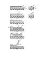
以下、図2(A)~(H)を用いて、本発明に係るシリコン系細線光導波路の他の加工方法を説明する。
図2(A)及びその側面図(B)の工程及び(E)~(H)の工程は、第1の実施形態のものとほぼ同様であるから詳しい説明を省略する。
第2の実施形態では、図2(A)及びその側面図(B)の工程に引き続いて、図2(C)に示すように、シリコン系細線光導波路13の端部15の下部の支持層12を除去して片持ち梁構造を形成する。
次に、片持ち梁構造を形成したシリコン基板11に、図2(E)に示すように、基板上方の特定の方位よりイオンビームを照射し、図2(F)に示すように、片持ち梁構造全体にわたって上方向に湾曲させる。
なおここで、保護膜14がSiO2膜のようにシリコン系細線光導波路のクラッドとして機能するものであれば除去する必要はなくそのまま使用することもできるが、メタルのように質量が重い材料からなる場合には樹脂やガラス等の低屈折率材料層17の埋め込みの前に除去する必要がある。
以下、図3(A)~(H)を用いて、本発明に係るシリコン系細線光導波路の他の加工方法を説明する。
第3の実施形態は、第1、第2の実施形態の変形例である。
図3(A)~(E)の工程は、第1の実施形態のものとほぼ同様であるから詳しい説明を省略する。
第3の実施形態では、図3(E)の工程に引き続いて、図3(F)に示すように、片持ち梁構造の周囲及びシリコン系細線光導波路13の上に、例えばCVD法により第2の保護膜19を形成する。
なおここで、保護膜14、第2の保護膜19がSiO2膜のようにシリコン系細線光導波路のクラッドとして機能するものであれば除去する必要はなくそのまま使用することもできるが、保護膜14、第2の保護膜19がメタルのように質量が重い材料からなる場合には、樹脂やガラス等の低屈折率材料層の埋め込みの前にそれぞれ除去する必要がある。
以下、図4(A)~(I)を用いて、本発明に係るシリコン系細線光導波路のさらに他の加工方法を説明する。
図4(A)~(D)の工程及び(F)~(I)の工程は、第2の実施形態のものとほぼ同様であるから詳しい説明を省略する。
第4の実施形態では、図4(A)~(D)の工程に引き続いて、図4(E)に示すように、片持ち梁構造のシリコン系細線光導波路13の端部15の上の保護膜14の一部を除去する。
なおここで、保護膜14がSiO2膜のようにシリコン系細線光導波路のクラッドとして機能するものであれば除去する必要はなくそのまま使用することもできるが、メタルのように質量が重い材料からなる場合には樹脂やガラス等の低屈折率材料層17の埋め込みの前に除去する必要がある。
(1)第1ないし第3の実施形態のものより急峻な湾曲部を形成することができる。
(2)保護膜の欠如部分に有効にイオンが注入できるため、第2、第3の実施形態のものより低ドーズで湾曲部を形成することができる。
(3)細線光導波路の端部の一部にも保護膜が形成されているため、第1の実施形態のものより光伝搬損失は小さい。
すなわち、本発明は、特許請求の範囲を逸脱しない限り、シリコン系細線光導波路の加工に当たって、適宜の設計変更が可能であることは言うまでもないことである。
さらに、本発明において細線光導波路のコア構造に使用するシリコン系材料としては、結晶シリコン等の第一コア材を被覆して第二コア材として用いられる酸化シリコンあるいは窒化シリコンや窒化酸化シリコンなどのシリコン化合物であっても、上記各実施形態で述べたと同様の作用効果が得られる。
2 支持層
3 シリコン系細線光導波路
4 シリコン系細線光導波路の端部
11 シリコン基板
12 支持層
13 シリコン系細線光導波路
14 保護膜
15 シリコン系細線光導波路の端部
16 シリコン系細線光導波路の末端部
17 低屈折率材料層
18 光デバイス
19 第2の保護膜
Claims (11)
- 支持層を介して複数のシリコン系細線光導波路が形成された光回路基板を用意する工程と、シリコン系細線光導波路のうち端部を有する所望のシリコン系細線光導波路に対して、該シリコン系細線光導波路の端部の下の支持層を除去する工程と、該シリコン系細線光導波路の端部を除いた該シリコン系細線光導波路の上に保護膜を選択的に形成する工程と、該シリコン系細線光導波路に対して特定の方向からイオンを打ち込むことにより、該特定の方向にセルフアライメント的に該シリコン系細線光導波路の端部を湾曲させる工程とを備えたシリコン系細線光導波路の加工方法。
- 支持層を介して複数のシリコン系細線光導波路が形成された光回路基板を用意する工程と、シリコン系細線光導波路のうち端部を有する所望のシリコン系細線光導波路に対して、該シリコン系細線光導波路の端部の下の支持層を除去する工程と、該シリコン系細線光導波路の端部を含む該シリコン系細線光導波路の上に保護膜を形成する工程と、該シリコン系細線光導波路に対して特定の方向からイオンを打ち込むことにより、該特定の方向にセルフアライメント的に該シリコン系細線光導波路の端部を湾曲させる工程とを備えたシリコン系細線光導波路の加工方法。
- 支持層を介して複数のシリコン系細線光導波路が形成された光回路基板を用意する工程と、シリコン系細線光導波路のうち端部を有する所望のシリコン系細線光導波路に対して、該シリコン系細線光導波路の端部の下の支持層を除去する工程と、該シリコン系細線光導波路の端部を除いた該シリコン系細線光導波路の上に保護膜を選択的に形成する工程と、該シリコン系細線光導波路の端部の上及び該保護膜の上に第2の保護膜を形成する工程と、該シリコン系細線光導波路に対して特定の方向からイオンを打ち込むことにより、該特定の方向にセルフアライメント的に該シリコン系細線光導波路の端部を湾曲させる工程とを備えたシリコン系細線光導波路の加工方法。
- 支持層を介して複数のシリコン系細線光導波路が形成された光回路基板を用意する工程と、シリコン系細線光導波路のうち端部を有する所望のシリコン系細線光導波路に対して、該シリコン系細線光導波路の端部の下の支持層を除去する工程と、該シリコン系細線光導波路の端部を含む該シリコン系細線光導波路の上に保護膜を形成する工程と、該該シリコン系細線光導波路の端部の上の保護膜の一部を選択的に除去する工程と、該シリコン系細線光導波路に対して特定の方向からイオンを打ち込むことにより、該特定の方向にセルフアライメント的に該シリコン系細線光導波路の端部の一部を湾曲させる工程とを備えたシリコン系細線光導波路の加工方法。
- さらに、湾曲された該シリコン系細線光導波路の末端部が埋設されるように、上記光回路基板上に低屈折率材料層を形成する工程とを備えた請求項1ないし4のいずれか1項に記載のシリコン系細線光導波路の加工方法。
- 湾曲した上記末端部に光デバイスを設置する工程をさらに備えた請求項5に記載のシリコン系細線光導波路の加工方法。
- 上記光デバイスは、光ファイバーであることを特徴とする請求項6に記載のシリコン系細線光導波路の加工方法。
- 上記光デバイスは、フォトディテクターであることを特徴とする請求項6に記載のシリコン系細線光導波路の加工方法。
- 上記イオンは、Siイオンであることを特徴とする請求項1ないし請求項8のいずれか1項に記載のシリコン系細線光導波路の加工方法。
- 上記保護膜は、シリコン系細線光導波路のクラッドとして機能することを特徴とする請求項1ないし請求項5のいずれか1項に記載のシリコン系細線光導波路の加工方法。
- 上記保護膜は、質量が重い材料からなり、上記湾曲された該シリコン系細線光導波路の末端部が埋設されるように、上記光回路基板上に低屈折率材料層を形成する工程の前に除去されることを特徴とする請求項5に記載のシリコン系細線光導波路の加工方法。
Priority Applications (2)
| Application Number | Priority Date | Filing Date | Title |
|---|---|---|---|
| US14/779,921 US9442249B2 (en) | 2013-03-25 | 2014-01-20 | Method for processing silicon-based wire optical waveguide |
| JP2015508112A JP6132369B2 (ja) | 2013-03-25 | 2014-01-20 | シリコン系細線光導波路の加工方法 |
Applications Claiming Priority (2)
| Application Number | Priority Date | Filing Date | Title |
|---|---|---|---|
| JP2013062421 | 2013-03-25 | ||
| JP2013-062421 | 2013-03-25 |
Publications (1)
| Publication Number | Publication Date |
|---|---|
| WO2014156233A1 true WO2014156233A1 (ja) | 2014-10-02 |
Family
ID=51623238
Family Applications (1)
| Application Number | Title | Priority Date | Filing Date |
|---|---|---|---|
| PCT/JP2014/050909 Ceased WO2014156233A1 (ja) | 2013-03-25 | 2014-01-20 | シリコン系細線光導波路の加工方法 |
Country Status (3)
| Country | Link |
|---|---|
| US (1) | US9442249B2 (ja) |
| JP (1) | JP6132369B2 (ja) |
| WO (1) | WO2014156233A1 (ja) |
Cited By (1)
| Publication number | Priority date | Publication date | Assignee | Title |
|---|---|---|---|---|
| JP2018097274A (ja) * | 2016-12-15 | 2018-06-21 | 国立研究開発法人産業技術総合研究所 | 光結合器 |
Families Citing this family (6)
| Publication number | Priority date | Publication date | Assignee | Title |
|---|---|---|---|---|
| GB201313592D0 (en) * | 2013-07-30 | 2013-09-11 | Univ St Andrews | Optical modulator with plasmon based coupling |
| US9594220B1 (en) * | 2015-09-22 | 2017-03-14 | Corning Optical Communications LLC | Optical interface device having a curved waveguide using laser writing and methods of forming |
| US10422950B2 (en) * | 2017-02-20 | 2019-09-24 | Corning Optical Communications LLC | Laminated glass bend optical interconnection apparatus and methods |
| WO2019035466A1 (ja) * | 2017-08-16 | 2019-02-21 | Agc株式会社 | ポリマー光導波路 |
| JP2019219619A (ja) * | 2018-06-22 | 2019-12-26 | ルネサスエレクトロニクス株式会社 | 半導体装置およびその製造方法 |
| NL2026563B1 (en) * | 2020-09-28 | 2022-05-30 | Photonip B V | Optical assembly |
Citations (2)
| Publication number | Priority date | Publication date | Assignee | Title |
|---|---|---|---|---|
| US8442368B1 (en) * | 2010-01-22 | 2013-05-14 | The Ohio State University Research Foundation | Cantilever couplers for intra-chip coupling to photonic integrated circuits |
| JP2013178333A (ja) * | 2012-02-28 | 2013-09-09 | National Institute Of Advanced Industrial & Technology | シリコン細線光導波路の加工方法 |
Family Cites Families (1)
| Publication number | Priority date | Publication date | Assignee | Title |
|---|---|---|---|---|
| US8744222B2 (en) * | 2011-07-27 | 2014-06-03 | National Applied Research Laboratories | Practical silicon photonic multi-function integrated-optic chip for fiber sensor applications |
-
2014
- 2014-01-20 JP JP2015508112A patent/JP6132369B2/ja active Active
- 2014-01-20 US US14/779,921 patent/US9442249B2/en active Active
- 2014-01-20 WO PCT/JP2014/050909 patent/WO2014156233A1/ja not_active Ceased
Patent Citations (2)
| Publication number | Priority date | Publication date | Assignee | Title |
|---|---|---|---|---|
| US8442368B1 (en) * | 2010-01-22 | 2013-05-14 | The Ohio State University Research Foundation | Cantilever couplers for intra-chip coupling to photonic integrated circuits |
| JP2013178333A (ja) * | 2012-02-28 | 2013-09-09 | National Institute Of Advanced Industrial & Technology | シリコン細線光導波路の加工方法 |
Non-Patent Citations (5)
| Title |
|---|
| JUN KIMIN ET AL., JOURNAL OF VACUUM SCIENCE & TECHNOLOGY B, vol. 27, no. 6, November 2009 (2009-11-01), pages 3043 - 3047 * |
| SUN PENG ET AL., OPTICS EXPRESS, vol. 17, no. 6, 16 March 2009 (2009-03-16), pages 4565 - 4574 * |
| SUN PENG ET AL., OPTICS EXPRESS, vol. 19, no. 5, 28 February 2011 (2011-02-28), pages 4722 - 4727 * |
| TOMOYA YOSHIDA ET AL.: "Ion Chunyu Gijutsu o Oyo shita Rittai Mage Doharo no Sakusei", DAI 74 KAI THE JAPAN SOCIETY OF APPLIED PHYSICS SHUKI GAKUJUTSU KOENKAI KOEN YOKOSHU, 31 August 2013 (2013-08-31) * |
| YOSHIDA T. ET AL., 10TH INTERNATIONAL CONFERENCE ON GROUP IV PHOTONICS (GFP, vol. 08, 2013, pages 89 - 90 * |
Cited By (1)
| Publication number | Priority date | Publication date | Assignee | Title |
|---|---|---|---|---|
| JP2018097274A (ja) * | 2016-12-15 | 2018-06-21 | 国立研究開発法人産業技術総合研究所 | 光結合器 |
Also Published As
| Publication number | Publication date |
|---|---|
| US9442249B2 (en) | 2016-09-13 |
| JP6132369B2 (ja) | 2017-05-24 |
| JPWO2014156233A1 (ja) | 2017-02-16 |
| US20160047979A1 (en) | 2016-02-18 |
Similar Documents
| Publication | Publication Date | Title |
|---|---|---|
| JP6132369B2 (ja) | シリコン系細線光導波路の加工方法 | |
| JP5129350B2 (ja) | 光ファイバおよび高インデックス差導波路を特にカップリングさせるための光モード変換器 | |
| JP5677456B2 (ja) | 高速光i/o用途向けの集積受光器アーキテクチャ、方法及びシステム | |
| KR101591847B1 (ko) | 효율적인 실리콘-온-인슐레이터 격자 결합기 | |
| US8494315B2 (en) | Photonic integrated circuit having a waveguide-grating coupler | |
| US8442368B1 (en) | Cantilever couplers for intra-chip coupling to photonic integrated circuits | |
| CN107111064B (zh) | 与硅波导水平耦合 | |
| JP2005538426A (ja) | 埋め込みモードコンバータ | |
| EP3296783A1 (en) | Integrated photonics waveguide grating coupler | |
| EP3149522A1 (en) | Waveguide mode expander using amorphous silicon | |
| JP2004184986A (ja) | 光学素子およびその製造方法 | |
| Pearson et al. | Arrayed waveguide grating demultiplexers in silicon-on-insulator | |
| CN107077014B (zh) | 光学衰减器及其制造方法 | |
| JP5794574B2 (ja) | シリコン細線光導波路の加工方法 | |
| JP5386254B2 (ja) | スポットサイズ変換光導波路部を有する光学素子 | |
| KR20160092565A (ko) | 평탄한 모드 발생 장치 및 이를 구비하는 배열 도파로 격자 | |
| Yoshida et al. | Elephant coupler: vertically curved Si waveguide with wide and flat wavelength window insensitive to coupling angle | |
| JP4195992B2 (ja) | スポットサイズ変換器の製造方法 | |
| JP2005326876A (ja) | 光導波路 | |
| Song et al. | Focusing grating couplers in unmodified 180-nm silicon-on-insulator CMOS | |
| Sanchis et al. | Experimental demonstration of high coupling efficiency between wide ridge waveguides and single-mode photonic crystal waveguides | |
| Zhou et al. | A novel highly efficient grating coupler with large filling factor used for optoelectronic integration | |
| Van Thourhout et al. | Functional silicon wire waveguides | |
| JP6325941B2 (ja) | 光回路 | |
| Chen et al. | Optical Waveguides by Germanium Ion Implantation on Silicon-on-Insulator Platform |
Legal Events
| Date | Code | Title | Description |
|---|---|---|---|
| 121 | Ep: the epo has been informed by wipo that ep was designated in this application |
Ref document number: 14775692 Country of ref document: EP Kind code of ref document: A1 |
|
| ENP | Entry into the national phase |
Ref document number: 2015508112 Country of ref document: JP Kind code of ref document: A |
|
| WWE | Wipo information: entry into national phase |
Ref document number: 14779921 Country of ref document: US |
|
| NENP | Non-entry into the national phase |
Ref country code: DE |
|
| 122 | Ep: pct application non-entry in european phase |
Ref document number: 14775692 Country of ref document: EP Kind code of ref document: A1 |