WO2014148220A1 - 導光板の製造方法、照明装置の製造方法、及び表示装置の製造方法 - Google Patents
導光板の製造方法、照明装置の製造方法、及び表示装置の製造方法 Download PDFInfo
- Publication number
- WO2014148220A1 WO2014148220A1 PCT/JP2014/054813 JP2014054813W WO2014148220A1 WO 2014148220 A1 WO2014148220 A1 WO 2014148220A1 JP 2014054813 W JP2014054813 W JP 2014054813W WO 2014148220 A1 WO2014148220 A1 WO 2014148220A1
- Authority
- WO
- WIPO (PCT)
- Prior art keywords
- plate
- processed
- light guide
- end surface
- guide plate
- Prior art date
- Legal status (The legal status is an assumption and is not a legal conclusion. Google has not performed a legal analysis and makes no representation as to the accuracy of the status listed.)
- Ceased
Links
Images








Classifications
-
- G—PHYSICS
- G02—OPTICS
- G02B—OPTICAL ELEMENTS, SYSTEMS OR APPARATUS
- G02B6/00—Light guides; Structural details of arrangements comprising light guides and other optical elements, e.g. couplings
- G02B6/0001—Light guides; Structural details of arrangements comprising light guides and other optical elements, e.g. couplings specially adapted for lighting devices or systems
- G02B6/0011—Light guides; Structural details of arrangements comprising light guides and other optical elements, e.g. couplings specially adapted for lighting devices or systems the light guides being planar or of plate-like form
- G02B6/0065—Manufacturing aspects; Material aspects
-
- B—PERFORMING OPERATIONS; TRANSPORTING
- B29—WORKING OF PLASTICS; WORKING OF SUBSTANCES IN A PLASTIC STATE IN GENERAL
- B29C—SHAPING OR JOINING OF PLASTICS; SHAPING OF MATERIAL IN A PLASTIC STATE, NOT OTHERWISE PROVIDED FOR; AFTER-TREATMENT OF THE SHAPED PRODUCTS, e.g. REPAIRING
- B29C59/00—Surface shaping of articles, e.g. embossing; Apparatus therefor
- B29C59/002—Component parts, details or accessories; Auxiliary operations
-
- B—PERFORMING OPERATIONS; TRANSPORTING
- B29—WORKING OF PLASTICS; WORKING OF SUBSTANCES IN A PLASTIC STATE IN GENERAL
- B29C—SHAPING OR JOINING OF PLASTICS; SHAPING OF MATERIAL IN A PLASTIC STATE, NOT OTHERWISE PROVIDED FOR; AFTER-TREATMENT OF THE SHAPED PRODUCTS, e.g. REPAIRING
- B29C59/00—Surface shaping of articles, e.g. embossing; Apparatus therefor
- B29C59/005—Surface shaping of articles, e.g. embossing; Apparatus therefor characterised by the choice of material
-
- B—PERFORMING OPERATIONS; TRANSPORTING
- B29—WORKING OF PLASTICS; WORKING OF SUBSTANCES IN A PLASTIC STATE IN GENERAL
- B29C—SHAPING OR JOINING OF PLASTICS; SHAPING OF MATERIAL IN A PLASTIC STATE, NOT OTHERWISE PROVIDED FOR; AFTER-TREATMENT OF THE SHAPED PRODUCTS, e.g. REPAIRING
- B29C59/00—Surface shaping of articles, e.g. embossing; Apparatus therefor
- B29C59/02—Surface shaping of articles, e.g. embossing; Apparatus therefor by mechanical means, e.g. pressing
- B29C59/022—Surface shaping of articles, e.g. embossing; Apparatus therefor by mechanical means, e.g. pressing characterised by the disposition or the configuration, e.g. dimensions, of the embossments or the shaping tools therefor
-
- B—PERFORMING OPERATIONS; TRANSPORTING
- B29—WORKING OF PLASTICS; WORKING OF SUBSTANCES IN A PLASTIC STATE IN GENERAL
- B29D—PRODUCING PARTICULAR ARTICLES FROM PLASTICS OR FROM SUBSTANCES IN A PLASTIC STATE
- B29D11/00—Producing optical elements, e.g. lenses or prisms
- B29D11/00663—Production of light guides
- B29D11/00721—Production of light guides involving preforms for the manufacture of light guides
-
- G—PHYSICS
- G02—OPTICS
- G02B—OPTICAL ELEMENTS, SYSTEMS OR APPARATUS
- G02B6/00—Light guides; Structural details of arrangements comprising light guides and other optical elements, e.g. couplings
- G02B6/0001—Light guides; Structural details of arrangements comprising light guides and other optical elements, e.g. couplings specially adapted for lighting devices or systems
- G02B6/0011—Light guides; Structural details of arrangements comprising light guides and other optical elements, e.g. couplings specially adapted for lighting devices or systems the light guides being planar or of plate-like form
- G02B6/0013—Means for improving the coupling-in of light from the light source into the light guide
- G02B6/0015—Means for improving the coupling-in of light from the light source into the light guide provided on the surface of the light guide or in the bulk of it
- G02B6/002—Means for improving the coupling-in of light from the light source into the light guide provided on the surface of the light guide or in the bulk of it by shaping at least a portion of the light guide, e.g. with collimating, focussing or diverging surfaces
-
- G—PHYSICS
- G02—OPTICS
- G02F—OPTICAL DEVICES OR ARRANGEMENTS FOR THE CONTROL OF LIGHT BY MODIFICATION OF THE OPTICAL PROPERTIES OF THE MEDIA OF THE ELEMENTS INVOLVED THEREIN; NON-LINEAR OPTICS; FREQUENCY-CHANGING OF LIGHT; OPTICAL LOGIC ELEMENTS; OPTICAL ANALOGUE/DIGITAL CONVERTERS
- G02F1/00—Devices or arrangements for the control of the intensity, colour, phase, polarisation or direction of light arriving from an independent light source, e.g. switching, gating or modulating; Non-linear optics
- G02F1/01—Devices or arrangements for the control of the intensity, colour, phase, polarisation or direction of light arriving from an independent light source, e.g. switching, gating or modulating; Non-linear optics for the control of the intensity, phase, polarisation or colour
- G02F1/13—Devices or arrangements for the control of the intensity, colour, phase, polarisation or direction of light arriving from an independent light source, e.g. switching, gating or modulating; Non-linear optics for the control of the intensity, phase, polarisation or colour based on liquid crystals, e.g. single liquid crystal display cells
- G02F1/133—Constructional arrangements; Operation of liquid crystal cells; Circuit arrangements
- G02F1/1333—Constructional arrangements; Manufacturing methods
- G02F1/1335—Structural association of cells with optical devices, e.g. polarisers or reflectors
- G02F1/1336—Illuminating devices
- G02F1/133602—Direct backlight
- G02F1/133608—Direct backlight including particular frames or supporting means
-
- G—PHYSICS
- G03—PHOTOGRAPHY; CINEMATOGRAPHY; ANALOGOUS TECHNIQUES USING WAVES OTHER THAN OPTICAL WAVES; ELECTROGRAPHY; HOLOGRAPHY
- G03F—PHOTOMECHANICAL PRODUCTION OF TEXTURED OR PATTERNED SURFACES, e.g. FOR PRINTING, FOR PROCESSING OF SEMICONDUCTOR DEVICES; MATERIALS THEREFOR; ORIGINALS THEREFOR; APPARATUS SPECIALLY ADAPTED THEREFOR
- G03F7/00—Photomechanical, e.g. photolithographic, production of textured or patterned surfaces, e.g. printing surfaces; Materials therefor, e.g. comprising photoresists; Apparatus specially adapted therefor
- G03F7/0002—Lithographic processes using patterning methods other than those involving the exposure to radiation, e.g. by stamping
-
- B—PERFORMING OPERATIONS; TRANSPORTING
- B29—WORKING OF PLASTICS; WORKING OF SUBSTANCES IN A PLASTIC STATE IN GENERAL
- B29C—SHAPING OR JOINING OF PLASTICS; SHAPING OF MATERIAL IN A PLASTIC STATE, NOT OTHERWISE PROVIDED FOR; AFTER-TREATMENT OF THE SHAPED PRODUCTS, e.g. REPAIRING
- B29C59/00—Surface shaping of articles, e.g. embossing; Apparatus therefor
- B29C59/02—Surface shaping of articles, e.g. embossing; Apparatus therefor by mechanical means, e.g. pressing
- B29C59/022—Surface shaping of articles, e.g. embossing; Apparatus therefor by mechanical means, e.g. pressing characterised by the disposition or the configuration, e.g. dimensions, of the embossments or the shaping tools therefor
- B29C2059/023—Microembossing
-
- B—PERFORMING OPERATIONS; TRANSPORTING
- B29—WORKING OF PLASTICS; WORKING OF SUBSTANCES IN A PLASTIC STATE IN GENERAL
- B29K—INDEXING SCHEME ASSOCIATED WITH SUBCLASSES B29B, B29C OR B29D, RELATING TO MOULDING MATERIALS OR TO MATERIALS FOR MOULDS, REINFORCEMENTS, FILLERS OR PREFORMED PARTS, e.g. INSERTS
- B29K2069/00—Use of PC, i.e. polycarbonates or derivatives thereof, as moulding material
-
- B—PERFORMING OPERATIONS; TRANSPORTING
- B29—WORKING OF PLASTICS; WORKING OF SUBSTANCES IN A PLASTIC STATE IN GENERAL
- B29K—INDEXING SCHEME ASSOCIATED WITH SUBCLASSES B29B, B29C OR B29D, RELATING TO MOULDING MATERIALS OR TO MATERIALS FOR MOULDS, REINFORCEMENTS, FILLERS OR PREFORMED PARTS, e.g. INSERTS
- B29K2105/00—Condition, form or state of moulded material or of the material to be shaped
- B29K2105/25—Solid
- B29K2105/253—Preform
- B29K2105/256—Sheets, plates, blanks or films
-
- B—PERFORMING OPERATIONS; TRANSPORTING
- B29—WORKING OF PLASTICS; WORKING OF SUBSTANCES IN A PLASTIC STATE IN GENERAL
- B29L—INDEXING SCHEME ASSOCIATED WITH SUBCLASS B29C, RELATING TO PARTICULAR ARTICLES
- B29L2011/00—Optical elements, e.g. lenses, prisms
- B29L2011/0075—Light guides, optical cables
-
- G—PHYSICS
- G02—OPTICS
- G02F—OPTICAL DEVICES OR ARRANGEMENTS FOR THE CONTROL OF LIGHT BY MODIFICATION OF THE OPTICAL PROPERTIES OF THE MEDIA OF THE ELEMENTS INVOLVED THEREIN; NON-LINEAR OPTICS; FREQUENCY-CHANGING OF LIGHT; OPTICAL LOGIC ELEMENTS; OPTICAL ANALOGUE/DIGITAL CONVERTERS
- G02F1/00—Devices or arrangements for the control of the intensity, colour, phase, polarisation or direction of light arriving from an independent light source, e.g. switching, gating or modulating; Non-linear optics
- G02F1/01—Devices or arrangements for the control of the intensity, colour, phase, polarisation or direction of light arriving from an independent light source, e.g. switching, gating or modulating; Non-linear optics for the control of the intensity, phase, polarisation or colour
- G02F1/13—Devices or arrangements for the control of the intensity, colour, phase, polarisation or direction of light arriving from an independent light source, e.g. switching, gating or modulating; Non-linear optics for the control of the intensity, phase, polarisation or colour based on liquid crystals, e.g. single liquid crystal display cells
- G02F1/133—Constructional arrangements; Operation of liquid crystal cells; Circuit arrangements
- G02F1/1333—Constructional arrangements; Manufacturing methods
- G02F1/1335—Structural association of cells with optical devices, e.g. polarisers or reflectors
- G02F1/1336—Illuminating devices
- G02F1/133628—Illuminating devices with cooling means
Definitions
- the present invention relates to a light guide plate manufacturing method, a lighting device manufacturing method, and a display device manufacturing method.
- an edge light type backlight device is known as an example of a backlight device used in a liquid crystal display device.
- a light guide plate for guiding light emitted from a light source to the display surface side may be arranged in the housing.
- Such a light guide plate is usually formed primarily by punching a base material for forming a light guide plate made of resin or the like with a frame-shaped mold.
- Patent Document 1 discloses a method for forming a light guide plate.
- a molded light guide plate is primarily formed by extrusion molding a resin plate, and a stamper having a pattern or a smooth surface formed as a part of the heating plate is brought into contact with the end surface of the molded light guide plate. Then, the pattern or smooth surface is transferred to the end face by heating and pressurizing.
- the technology disclosed in this specification has been created in view of the above problems. It is an object of the present specification to provide a technique capable of manufacturing a light guide plate with improved light incident quality from the end face while preventing or suppressing the occurrence of burrs at both ends of the end face. .
- the technology disclosed in the present specification includes a punching step of punching a base material for forming a light guide plate with a frame-shaped die to form a punched plate having an end surface made rectangular from the base material, and the punching plate.
- a thermal transfer step of thermally transferring a pattern of the processed surface to the end surface by pressing a processed surface provided on the heated processed plate against at least one end surface of the processed surface, wherein the processed surface is the end surface
- a light guide plate with improved surface accuracy and improved light incident quality from the end face can be manufactured.
- the processed surface of the processed plate is a flat surface
- the portion on the center side in the long side direction of the end surface is crushed so that the longer side direction
- the burr may occur at both ends of the end face in the long side direction.
- the processed surface having a recessed shape on the side facing the central side in the long side direction of the end surface of the punched plate is pressed against the end surface, so the long side of the end surface It will be crushed by the processing surface in order from the part on both ends in the direction toward the part on the center side. For this reason, it can prevent thru
- the manufacturing method described above it is possible to manufacture a light guide plate with improved light incident quality from the end face while preventing or suppressing the occurrence of burrs at both ends of the end face.
- the processed plate may be pressed against at least one end surface of the punched plate that faces the light source.
- this manufacturing method it is possible to manufacture a light guide plate in which the surface accuracy of the end surface on the side facing the light source is improved. For this reason, brightness
- the processed plate may be pressed against all end faces of the punched plate. According to this manufacturing method, it is possible to manufacture a light guide plate in which the surface accuracy of all end faces is improved, and thereby it is possible to further improve the luminance of a lighting device or the like including the light guide plate.
- the processed plate whose processed surface is a smooth surface by mirror processing may be pressed against the end surface.
- the light incident efficiency at the end surface can be improved by pressing the end surface with a processed surface that is a smooth surface by mirror processing. For this reason, brightness
- the processed plate having a roughened processed surface may be pressed against the end surface.
- this manufacturing method it is possible to manufacture a light guide plate whose end surface is a rough surface with high accuracy. By arranging the light source so as to face the end surface according to the rough surface pattern, it is possible to prevent or suppress luminance unevenness or the like generated between adjacent light sources.
- the processed plate provided with the finely processed pattern on the processed surface may be pressed against the end surface.
- this manufacturing method it is possible to manufacture a light guide plate whose end surface is a finely processed surface with high accuracy. By arranging the light source so as to face the end surface according to the pattern of the finely processed surface, it is possible to prevent or suppress luminance unevenness generated between adjacent light sources.
- the processed plate in which the finely processed pattern has a wavy pattern along the long side direction of the end surface may be pressed against the end surface.
- this manufacturing method it is possible to manufacture a light guide plate whose end surface is a highly accurate wavy line finely processed surface.
- the processed plate may be pressed against the end surface while the punched plate is held with respect to the long side direction of the end surface. According to this manufacturing method, the punching plate is prevented or suppressed from shifting in the long side direction in the thermal transfer process, and therefore the end surface of the punching plate can be satisfactorily processed with the processed plate.
- the technology disclosed in the present specification is a manufacturing of a lighting device including a step of manufacturing a light guide plate by the above manufacturing method, and a light source assembly step of mounting a light source so as to face at least one of the end surfaces of the light guide plate. It may be a method.
- a method of manufacturing a display device comprising: a step of manufacturing a lighting device by the above manufacturing method; and a display panel assembling step of mounting a display panel on the lighting device in a form opposite to one plate surface of the light guide plate. There may be.
- FIG. 1 is an exploded perspective view showing a schematic configuration of a liquid crystal display device according to Embodiment 1.
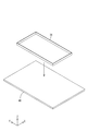
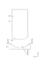
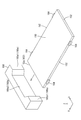
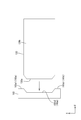
- FIG. The perspective view which shows the base material before performing a punching process The perspective view which shows the base material after performing the punching process The perspective view which shows the punching board before performing a thermal transfer process Plan view showing punched plate before thermal transfer process Plan view showing punched plate after performing thermal transfer process An enlarged photograph of the state of the end face of the punched plate before pressing the processed plate An enlarged photograph of the state of the end face of the punched plate after pressing the processed plate
- FIG. The top view which shows the punching board before performing a thermal transfer process in Embodiment 2.
- the top view of the processing board in Embodiment 3 The top view which expanded the site
- FIG. The top view which expanded some processing surfaces of the processing board in the modification of Embodiment 3.
- Embodiment 1 will be described with reference to the drawings.
- a liquid crystal display device (an example of a display device) 10 including the light guide plate 20 is illustrated.
- a part of each drawing shows an X-axis, a Y-axis, and a Z-axis, and each axis direction is drawn in a common direction in each drawing.
- the liquid crystal display device 10 has a vertically long rectangular shape as a whole, and a liquid crystal panel (an example of a display panel) 11 whose front side plate surface is a display surface for displaying an image, and liquid crystal A cover panel 12 disposed to face the display surface of the panel 11 and an external light source disposed on the opposite side of the cover panel 12 across the liquid crystal panel 11 and supplying light to the liquid crystal panel 11 And a backlight device (an example of a lighting device) 24. Furthermore, the liquid crystal display device 10 includes a casing 34 that houses the cover panel 12, the liquid crystal panel 11, and the backlight device 24.
- the liquid crystal display device 10 includes a portable information terminal (such as a mobile phone, a smartphone, and a tablet notebook computer), an in-vehicle information terminal (such as a stationary car navigation system and a portable car navigation system), and a portable game. It is used for various electronic devices such as a machine. For this reason, the screen sizes of the liquid crystal panel 11 and the cover panel 12 constituting the liquid crystal display device 10 are about several inches to several tens of inches, and are generally classified as small or medium-sized.
- the liquid crystal panel 11 has a vertically long rectangular shape as a whole.
- the liquid crystal panel 11 has a transparent (translucent) glass CF substrate 11a, an array substrate 11b, and a space between both the substrates 11a and 11b. And a liquid crystal layer (not shown) including liquid crystal molecules that are substances whose optical characteristics change with application of an electric field.
- the cover panel 12 is arranged so as to cover the entire area of the liquid crystal panel 11 from the front side, whereby the liquid crystal panel 11 can be protected.
- the cover panel 12 is formed with a light shielding portion 12a that shields light around it.
- the casing 34 is made of a synthetic resin material or a metal material, and has a substantially bowl shape opened toward the front side as shown in FIG.
- a casing adhesive tape 32 is interposed between the casing 34 and the frame 22 constituting the backlight device 24, and the casing 34 and the frame 22 are kept in an attached state by the casing adhesive tape 32. It is supposed to be.
- the backlight device 24 includes an LED (Light Emitting Diode) 28 that is a light source, an LED 28, a flexible substrate 30, a light guide plate 20, an optical sheet 18, a reflection sheet 26, and a frame 22.
- the flexible substrate 30 has flexibility while being mounted with the LEDs 28.
- the light guide plate 20 guides the light emitted from the LEDs 28 to the liquid crystal panel 11 side.
- the optical sheet 18 is stacked on the light guide plate 20 and transmits the light emitted from the light guide plate 20 and emits the light toward the liquid crystal panel 11 while giving a predetermined optical action to the transmitted light.
- the reflection sheet 26 is disposed under the light guide plate 20 and reflects light leaked from the light guide plate 20.
- the frame 22 has a frame shape, surrounds the light guide plate 20 and the optical sheet 18, and supports the optical sheet 18 and the liquid crystal panel 11 from the back side (the side opposite to the cover panel 12 side). Note that a substantially frame-shaped panel adhesive tape 14 that adheres to both surfaces is interposed between the optical sheet 18 and the liquid crystal panel 11. The space between the sheet 18 and the sheet 18 is maintained.
- the light guide plate 20 is made of a synthetic resin material (for example, polycarbonate) having a refractive index sufficiently higher than that of air and substantially transparent (excellent translucency). As shown in FIG. 1, the light guide plate 20 has a rectangular shape in plan view and a thickness larger than that of the optical sheet 18, as in the liquid crystal panel 11. The X-axis direction and the long side direction coincide with the Y-axis direction, respectively, and the plate thickness direction perpendicular to the plate surface coincides with the Z-axis direction. The light guide plate 20 is disposed immediately below the liquid crystal panel 11 and the optical sheet 18 while being surrounded by the frame 22.
- a synthetic resin material for example, polycarbonate
- the surface facing the front side is a light emitting surface 20 b that emits internal light toward the optical sheet 18 and the liquid crystal panel 11. It has become.
- the plate surface (back surface) opposite to the light emitting surface 20b is an opposite surface 20c.
- one end surface (the left side shown in FIG. 1) of both end surfaces provided along the X-axis direction is mounted on the flexible substrate 30.
- the LED 28 is opposed to the LED 28 and serves as a light incident surface 20a on which light emitted from each LED 28 is incident.
- the light incident surface 20 a has an arc shape that bends along the X-axis direction. Even if the light incident surface 20a has such an arc shape, the light incident surface 20a can perform a function of causing light emitted from each LED 28 to enter.
- the light guide plate 20 introduces light emitted from each LED 28 from the light incident surface 20a, and rises toward the optical sheet 18 side (front side, light emission side) while propagating the light inside, thereby emitting the light. It has the function to emit from 20b.
- a method of manufacturing the light guide plate 20 will be described with reference to FIGS.
- a light guide plate forming base material 40 formed of the same material (synthetic resin material) as the material of the light guide plate 20 is prepared.
- the material of the light guide plate 20 and the material of the base material 40 are polycarbonate.
- a punching die 36 having a rectangular frame shape is moved in the vertical direction (Z-axis direction) against the heated base material 40 and pressed against the base material 40, and a punching press. Processing. Thereby, as shown in FIG.
- the punching plate 50 which forms the outline (rectangular outline) along the punching mark 40a of the punching die 36 from the base material 40 is formed (an example of the punching process).
- Each end surface 52 of the punched plate 50 after punching has a rectangular shape perpendicular to the plate surface of the punched plate 50.
- the punching die 36 may be a punching blade or a punching punch.
- the punching plate 50 is set on a base (not shown), and among the end surfaces 52 of the punching plate 50, end surfaces (hereinafter referred to as end surfaces to be processed) which are used as the light incident surfaces 20a in the light guide plate 20 after manufacture. Secondary processing is performed on 52a.
- the processed surface 60a of the heated processed plate 60 is pressed against the processed end surface 52a of the punched plate 50 having a rectangular shape in a posture parallel to the processed end surface 52a.
- the pattern of the processed surface 60a is thermally transferred to the processed end surface 52a (an example of a thermal transfer process).
- the processed surface 60a of the processed plate 60 is a processed part 60a2 in which a part facing the processed end surface 52a, that is, a part (a part on the central side) excluding the parts 60a1 on both ends is processed.
- the processed portion 60 a 2 is formed so that the center side in the long side direction of the processed end surface 52 a is closer to the opposite ends of the long side direction (X-axis direction) of the processed end surface 52 a.
- the opposing parts are recessed, and the entire surface is an arcuate curved surface.
- the processed surface 60a of the processed plate 60 is a smooth surface by mirror processing.
- the processing surface 60a of the processing plate 60 is pressed against the processed end surface 52a of the punching plate 50 by moving the punching plate 50 to the processing plate 60 side.
- the punching plate 50 is not displaced in the direction (X-axis direction) orthogonal to the direction (Y-axis direction) in which the punching plate 50 is moved. Further, both ends of the two end faces 52 adjacent to the work end face 52a are held by the holding members 64, respectively.
- the end face 52a to be processed is thermally transferred and shaped according to the pattern and shape of the processed portion 60a2 of the processed plate 60. Specifically, when the punching plate 50 is moved to the processed plate 60 side, the pattern of the processed portion 60a2 that has been made into a smooth surface by mirror finishing is thermally transferred to the processed end surface 52a, and the processed end surface 52a is made smooth. .
- the processing portion 60a2 of the processing plate 60 is arcuate as described above, so that the long side direction of the processing end surface 52a is in the long side direction.
- the parts on both ends in the (X-axis direction) abut on the processed plate 60 before the part on the center side in the long side direction.
- the processed plate 60 is pressed against the processed plate 60 in order from the part on both ends in the long side direction of the processed end surface 52a to the part on the center side.
- the entire end surface 52a to be processed is not pressed against the processing plate 60 at the same time, but the end surface 52a to be processed is shaped by being pressed against the processing plate 60 in order from both ends of the processing end surface 52a.
- the portion of the processed end surface 52a crushed by the processed plate 60 is directed from the both end sides of the processed end surface 52a toward the center side.
- the portions of the end surface 52a that are crushed by the processing plate 60 are prevented or suppressed from protruding from both ends of the end surface 52a. In other words, the occurrence of burrs is prevented or suppressed when the processed end face 52a is machined.
- the processed plate 60 heated to a temperature within the range of 150 ° C. to 180 ° C. is pressed against the processed end surface 52a.
- the processed plate 60 is pressed against the processed end surface 52a with a load of 200 gf (gravity gram) to 1500 gf.
- the time for pressing the processed plate 60 against the processed end surface 52a is set within a range of 10 seconds to 200 seconds.
- the processed end surface 52 a of the punched plate 50 is shaped by processing the shape of the processed end surface 52 a along the shape of the processed portion 60 a 2 of the processed plate 60 that is arcuate as described above.
- An arc shape is formed along the shape of the processing portion 60a2.
- the thermal transfer and the shape processing of the processed end surface 52a of the punching plate 50 are performed simultaneously.
- the light guide plate 20 of the present embodiment can be manufactured through the above steps.
- FIG. 7 shows an enlarged photograph of the state of the end face of the punched plate 50 before pressing the processed plate 60
- FIG. 8 shows the state of the end face 52 of the punched plate 50 after pressing the processed plate 60.
- Each enlarged photo is shown.
- the end surface 52 of the punched plate 50 after punching from the base material 40 has a rough surface accuracy, and its arithmetic average roughness (Ra) is 0.24. Incident efficiency is low.
- FIG. 8 as shown in FIG. 7, by performing secondary processing of pressing the processed plate 60 against the processed end surface 52 a of the punched plate 50 punched from the base material 40.
- the accuracy of the surface can be greatly improved as compared with the state, and the arithmetic average roughness (Ra) is 0.04, so that the incident efficiency of light on the processed end surface 52a can be increased.
- the incident efficiency and luminance of the end face 52 in the state of FIG. 7 are each 100%, the incident efficiency and luminance of the processed end face 52a in the state of FIG. 8 are improved to 105% and 110%, respectively.
- the LED 28 is assembled to the light guide plate 20 manufactured by the above method so as to face the light incident surface 20a (an example of a light source assembly process), and other members constituting the backlight device 24 are assembled.
- the backlight device 24 of the present embodiment can be manufactured.
- the liquid crystal panel 11 is assembled to the backlight device 24 (an example of a display panel assembling step), and then the cover panel 12 and the casing 34 are assembled to manufacture the liquid crystal display device 10 of the present embodiment. be able to.
- the processed surface 60a of the processed plate 60 is formed with respect to at least one end surface 52 of the punched plate 50 formed by punching the base material 40 for forming the light guide plate.
- the thermal transfer process of pressing the light guide plate 20 the surface accuracy of the end face 52 is improved, and the light guide plate 20 with improved light incident quality from the end face 52 can be manufactured.
- the processed surface of the processed plate is a flat surface, when the processed surface is pressed against the end surface of the punched plate, the portion on the center side in the long side direction of the end surface is crushed so that the longer side direction As a result, the burrs may be generated at both ends of the end face in the long side direction.
- the processed surface having a concave shape on the side facing the central side in the long side direction (X-axis direction) of the end surface 52 of the punched plate 50 Since 60 a is pressed against the end surface 52, the end surface 52 is crushed by the processing surface 60 a in order from the both end portions in the long side direction toward the central portion. For this reason, it can prevent thru
- the light guide plate 20 with improved light incident quality from the end surface 52 is obtained while preventing or suppressing the occurrence of burrs at both ends of the end surface 52. Can be manufactured.
- the end surface of the punched plate 50 is processed into the end surface facing the LED 28, that is, the end surface 52a that is the light incident surface 20a.
- the plate 60 is pressed against it.
- the processed plate 60 whose processed surface is a smooth surface by mirror processing is pressed against the end surface in the thermal transfer process.
- the processed surface 60a made into a smooth surface by mirror processing is pressed against the end surface 52, whereby the light incident efficiency on the end surface 52 can be improved.
- etc. Provided with the said light-guide plate 20 can be improved effectively.
- the processed plate 60 is pressed against the end surface 52 in a state where the punching plate 50 is held by the holding member 64 with respect to the long side direction of the end surface 52 in the thermal transfer process. It is said that.
- the punching plate 50 is prevented or suppressed from shifting in the long side direction in the thermal transfer process, and therefore the end surface 52 of the punching plate 50 can be satisfactorily processed by the processing plate 60.
- the rough surface pattern of the processed surface is adjusted, and the adjusted pattern is thermally transferred to the processed end surface of the punched plate to improve the incident quality of the processed end surface, and the light guide plate after manufacture In this case, it is possible to prevent or suppress the occurrence of luminance unevenness as described above.
- Embodiment 2 will be described with reference to FIGS. 9 to 11.
- the shape of the processed surface 160a of the processed plate 160 is different from that of the first embodiment. Since the other configuration is the same as that of the first embodiment, the description of the structure, operation, and effect is omitted. 9, 10, and 11, the parts obtained by adding the numeral 100 to the reference numerals in FIGS. 4, 5, and 6 are the same as the parts described in the first embodiment.
- the processed plate 160 having a processed surface 160 a different from that of the first embodiment is pressed against the processed end surface 152 a of the punched plate 150.
- the processed surface 160a of the processed plate 160 of the present embodiment is a processed part 160a2 in which a part (a part on the central side) excluding the parts 160a1 on both ends is processed, as in the first embodiment.
- This processed part 160a2 is configured by a flat surface, and as shown in FIGS. 9 and 10, the processed end surface 152a is more than the part facing both ends of the long side direction (X-axis direction) of the processed end surface 152a.
- part facing the center side of the long side direction is made into the shape which became depressed, and has comprised trapezoid shape as a whole.
- the processed end surface 152a of the punched plate 150 is processed by processing the shape of the processed end surface 152a along the shape of the processed portion 160a2 of the processed plate 160 having the trapezoidal shape.
- the shape is a trapezoid along the shape of the portion 160a2.
- Embodiment 3 will be described with reference to FIGS.
- the third embodiment is different from that of the first embodiment in that fine processing is performed on the processing surface 260a of the processing plate 260. Since the other configuration is the same as that of the first embodiment, the description of the structure, operation, and effect is omitted.
- the punched plate is subjected to secondary processing by pressing the processed plate 260 with the fine processing on the processed surface 260a against the processed end surface of the punched plate.
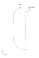
- the machining surface 260a of the machining plate 260 of the present embodiment has the same shape (arc shape) as that of the first embodiment as a whole, but a part of the machining site 260a2 of the machining surface 260a (one point in FIG. 12). When the portion surrounded by a chain line) is enlarged, a fine pattern of a wavy line pattern formed by straight lines as shown in FIG. 13 is applied.
- Such wavy line-shaped microfabrication can be realized by prism-shaped micromachining, cylinder-shaped micromachining, pyramid-shaped micromachining, or the like.
- the incident light quality of the processed end surface is improved, and the light guide plate after manufacture
- the occurrence of luminance unevenness as described in the first modification of the first embodiment can be prevented or suppressed.
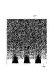
- FIG. 15 is an enlarged photograph showing the incident mode of light from the LED incident on the light incident surface 220a1 of the light guide plate 220A manufactured without performing the secondary processing of the punching plate 250.
- FIG. The enlarged photograph which shows the incident mode of the light from LED which injected into the light-incidence surface 220a2 of the light-guide plate 220B manufactured by performing the secondary process of the punching board 250 by the manufacturing method of a form is shown, respectively.
- FIG. 14 in the light guide plate 220A manufactured without performing the secondary processing of the punching plate 250, in the vicinity of the light incident surface 220a1, it faces each LED rather than a portion facing between adjacent LEDs.
- the part is displayed relatively brightly, and luminance unevenness occurs in which the part facing between adjacent LEDs is displayed relatively darker than the part facing each LED.
- the light guide plate 220B is manufactured by pressing the processed plate 260, which has been finely processed on the processed surface 260a, against the processed end surface of the punched plate, as shown in FIG. Compared with the case shown in FIG. 14, the luminance unevenness is greatly suppressed in the vicinity of the light incident surface 220a2 of the light guide plate 220B.
- the pattern to be thermally transferred to the end face of the punched plate can be changed as appropriate.
- SYMBOLS 10 Liquid crystal display device, 11 ... Liquid crystal panel, 12 ... Cover panel, 18 ... Optical sheet, 20, 120, 220A, 220B ... Light guide plate, 20a, 120a, 220a1, 220a2 ... Light incident surface, 22 ... Frame, 24 ... Backlight device, 34 ... casing, 36 ... punching die, 40 ... base material, 50, 150 ... punched plate, 52, 152 ... end face (of punched plate), 52a, 152a ... end face to be processed, 60, 160, 260 ... Processed plate, 60a, 160a, 260a ... Processed surface, 60a2, 160a2, 260a2 ... Processed part, 64, 164 ... Holding member
Landscapes
- Physics & Mathematics (AREA)
- Engineering & Computer Science (AREA)
- General Physics & Mathematics (AREA)
- Optics & Photonics (AREA)
- Manufacturing & Machinery (AREA)
- Mechanical Engineering (AREA)
- Nonlinear Science (AREA)
- Health & Medical Sciences (AREA)
- Ophthalmology & Optometry (AREA)
- Crystallography & Structural Chemistry (AREA)
- Chemical & Material Sciences (AREA)
- Mathematical Physics (AREA)
- Planar Illumination Modules (AREA)
Abstract
Description
しかしながら、上記特許文献1に記載された導光板の成形方法では、導光板の端面に平坦な面とされたスタンパを当接させる。このため、導光板の端面がスタンパによって押圧される際に、当該端面の中央側の部位が外側へと押し出されて拡がり、当該端面の両端からはみ出ることで、当該端面の両端にバリが発生する虞がある。
本明細書で開示される技術は、導光板成形用の基材を枠状の型で打ち抜くことで、該基材から端面が長方形状とされた打ち抜き板を形成する打ち抜き工程と、前記打ち抜き板の少なくとも一つの端面に加熱された加工板の板面に設けられた加工面を押し当てることで、該加工面のパターンを前記端面に熱転写する熱転写工程であって、前記加工面が前記端面の長辺方向の両端側と対向する部位よりも前記端面の長辺方向の中央側と対向する部位が窪んだ形状とされた前記加工板を前記端面に押し当てる熱転写工程と、を備える導光板の製造方法に関する。
この製造方法によると、光源と対向状に配される側の端面の面精度が向上された導光板を製造することができる。このため、当該導光板を備える照明装置等の輝度を効果的に向上させることができる。
この製造方法によると、全ての端面の面精度が向上された導光板を製造することができ、これにより、当該導光板を備える照明装置等の輝度を一層向上させることができる。
この製造方法によると、端面に鏡面加工による平滑面とされた加工面が押し当てられることで、当該端面における光の入射効率を向上させることができる。このため、当該導光板を備える照明装置等の輝度を効果的に向上させることができる。
この製造方法によると、端面が精度の高い粗面とされた導光板を製造することができる。この粗面のパターンに応じて光源を当該端面と対向状に配することにより、隣り合う光源間に発生する輝度ムラ等を防止ないし抑制することができる。
この製造方法によると、端面が精度の高い微細加工面とされた導光板を製造することができる。この微細加工面のパターンに応じて光源を当該端面と対向状に配することにより、隣り合う光源間に発生する輝度ムラ等を防止ないし抑制することができる。
この製造方法によると、端面が精度の高い波線状の微細加工面とされた導光板を製造することができる。この波線状をなす微細加工面のパターンの凹部と凸部とにそれぞれ対応させる形で光源を当該端面と対向状に配することにより、隣り合う光源間に発生する輝度ムラ等を効果的に防止ないし抑制することができる。
この製造方法によると、熱転写工程において打ち抜き板が長辺方向にずれることが防止ないし抑制されるため、打ち抜き板の端面を加工板によって良好に加工することができる。
本明細書で開示される技術によれば、端面の両端にバリが発生することを防止ないし抑制しながら、端面からの光の入射品位が向上された導光板を製造することができる。
図面を参照して実施形態1を説明する。本実施形態では、導光板20を備える液晶表示装置(表示装置の一例)10について例示する。なお、各図面の一部にはX軸、Y軸およびZ軸を示しており、各軸方向が各図面で共通した方向となるように描かれている。
続いて実施形態1の変形例1について説明する。変形例1における導光板の製造方法では、加工面が粗面とされた加工板を打ち抜き板の加工端面に押し当てる。ここで、並列状に配された複数のLEDと対向状に導光板が配された場合、導光板の光入射面近傍において、各LEDと対向する部位よりも隣接するLEDの間と対向する部位の方が相対的に暗く表示される輝度ムラが発生することがある。本変形例では、加工面の粗面のパターンを調整し、調整された当該パターンを打ち抜き板の被加工端面に熱転写することで、当該被加工端面の入射品位を向上させ、製造後の導光板において上記のような輝度ムラの発生を防止ないし抑制することができる。
続いて実施形態1の変形例2について説明する。変形例2における導光板20の製造方法では、打ち抜き板の全ての端面に加工板の加工面を押し当てる。このように打ち抜き板の全ての端面に加工板のパターンを熱転写することで、打ち抜き板の光入射面とされる端面にのみ加工板を押し当てる場合と比べて、製造後の導光板を用いたバックライト装置等の輝度を向上させることができる。
続いて図9ないし図11を参照して実施形態2を説明する。実施形態2は、加工板160の加工面160aの形状が実施形態1のものと異なっている。その他の構成については実施形態1のものと同様であるため、構造、作用、及び効果の説明は省略する。なお、図9、図10、図11において、それぞれ図4、図5、図6の参照符号に数字100を加えた部位は、実施形態1で説明した部位と同一である。
続いて図12ないし図15を参照して実施形態3を説明する。実施形態3は、加工板260の加工面260aに微細加工が施されている点で実施形態1のものと異なっている。その他の構成については実施形態1のものと同様であるため、構造、作用、及び効果の説明は省略する。
続いて実施形態3の変形例について説明する。変形例における導光板の製造方法では、加工面360aに施された微細加工の形状が異なる加工板を、打ち抜き板の被加工端面に押し当て、打ち抜き板の二次加工を行う。本変形例において、加工板360における加工面360aの加工部位360a2に施された微細加工の形状は、図16に示すように、曲線で構成された波線状とされている。加工面360aに施された微細加工がこのような形状とされている場合であっても、微細加工のパターンを調整し、調整された当該パターンを打ち抜き板の被加工端面に熱転写することで、当該被加工端面の入射品位を向上させ、製造後の導光板において実施形態1の変形例1で述べたような輝度ムラの発生を防止ないし抑制することができる。
本発明は上記既述及び図面によって説明した実施形態に限定されるものではなく、例えば次のような実施形態も本発明の技術的範囲に含まれる。
(1)上記の各実施形態では、加工面における加工部位が円弧状または台形状とされた加工板を抜き打ち板に押し当てる方法を例示したが、当該加工部位の形状は限定されない。加工面における加工部位が、抜き打ち板における被加工端面の長辺方向の両端側と対向する部位よりも被加工端面の長辺方向の中央側と対向する部位が窪んだ形状であればよい。
Claims (10)
- 導光板成形用の基材を枠状の型で打ち抜くことで、該基材から端面が長方形状とされた打ち抜き板を形成する打ち抜き工程と、
前記打ち抜き板の少なくとも一つの端面に加熱された加工板の板面に設けられた加工面を押し当てることで、該加工面のパターンを前記端面に熱転写する熱転写工程であって、前記加工面が前記端面の長辺方向の両端側と対向する部位よりも前記端面の長辺方向の中央側と対向する部位が窪んだ形状とされた前記加工板を前記端面に押し当てる熱転写工程と、
を備える導光板の製造方法。 - 前記熱転写工程では、前記打ち抜き板の端面のうち少なくとも光源と対向状に配される側の端面に前記加工板を押し当てる、請求項1に記載の導光板の製造方法。
- 前記熱転写工程では、前記打ち抜き板の全ての端面に前記加工板を押し当てる、請求項1または請求項2に記載の導光板の製造方法。
- 前記熱転写工程では、前記加工面が鏡面加工による平滑面とされた前記加工板を前記端面に押し当てる、請求項1から請求項3のいずれか1項に記載の導光板の製造方法。
- 前記熱転写工程では、前記加工面が粗面とされた前記前記加工板を前記端面に押し当てる、請求項1から請求項3のいずれか1項に記載の導光板の製造方法。
- 前記熱転写工程では、前記加工面に微細加工された前記パターンが設けられた前記加工板を前記端面に押し当てる、請求項1から請求項3のいずれか1項に記載の導光板の製造方法。
- 前記熱転写工程では、前記微細加工された前記パターンが前記端面の長辺方向に沿って波線状をなすパターンとされた前記加工板を前記端面に押し当てる、請求項6に記載の導光板の製造方法。
- 前記熱転写工程では、前記打ち抜き板を前記端面の長辺方向に対して保持した状態で前記加工板を前記端面に押し当てる、請求項1から請求項7のいずれか1項に記載の導光板の製造方法。
- 請求項1から請求項8のいずれか1項に記載の導光板の製造方法によって導光板を製造する工程と、
前記導光板の少なくとも一つの前記端面と対向状に光源を組み付ける光源組付工程と、
を備える照明装置の製造方法。 - 請求項9に記載の照明装置の製造方法によって照明装置を製造する工程と、
前記導光板の一方の板面と対向する形で前記照明装置に表示パネルを組み付ける表示パネル組付工程と、
を備える表示装置の製造方法。
Priority Applications (2)
| Application Number | Priority Date | Filing Date | Title |
|---|---|---|---|
| CN201480015820.6A CN105190155B (zh) | 2013-03-21 | 2014-02-27 | 导光板的制造方法、照明装置的制造方法以及显示装置的制造方法 |
| US14/778,175 US9939575B2 (en) | 2013-03-21 | 2014-02-27 | Method of manufacturing light guide plate, lighting device, and display device |
Applications Claiming Priority (2)
| Application Number | Priority Date | Filing Date | Title |
|---|---|---|---|
| JP2013058347 | 2013-03-21 | ||
| JP2013-058347 | 2013-03-21 |
Publications (1)
| Publication Number | Publication Date |
|---|---|
| WO2014148220A1 true WO2014148220A1 (ja) | 2014-09-25 |
Family
ID=51579911
Family Applications (1)
| Application Number | Title | Priority Date | Filing Date |
|---|---|---|---|
| PCT/JP2014/054813 Ceased WO2014148220A1 (ja) | 2013-03-21 | 2014-02-27 | 導光板の製造方法、照明装置の製造方法、及び表示装置の製造方法 |
Country Status (3)
| Country | Link |
|---|---|
| US (1) | US9939575B2 (ja) |
| CN (1) | CN105190155B (ja) |
| WO (1) | WO2014148220A1 (ja) |
Families Citing this family (1)
| Publication number | Priority date | Publication date | Assignee | Title |
|---|---|---|---|---|
| EP3438521B1 (en) * | 2016-03-30 | 2022-01-12 | Panasonic Intellectual Property Management Co., Ltd. | Display device |
Citations (3)
| Publication number | Priority date | Publication date | Assignee | Title |
|---|---|---|---|---|
| JP2004082437A (ja) * | 2002-08-26 | 2004-03-18 | Meiki Co Ltd | 導光板成形装置および導光板成形方法 |
| JP2011192489A (ja) * | 2010-03-12 | 2011-09-29 | Omron Corp | 導光板及び液晶表示装置 |
| JP2012079676A (ja) * | 2010-09-10 | 2012-04-19 | Asahi Kasei Corp | 導光部材 |
Family Cites Families (7)
| Publication number | Priority date | Publication date | Assignee | Title |
|---|---|---|---|---|
| JP2004351667A (ja) * | 2003-05-27 | 2004-12-16 | Hitachi Maxell Ltd | 一軸拡散面の製造方法およびこれを用いて製造された液晶表示装置用導光板、拡散シート、液晶表示装置 |
| CN100389330C (zh) * | 2004-12-11 | 2008-05-21 | 鸿富锦精密工业(深圳)有限公司 | 导光板制造方法 |
| US9027364B2 (en) * | 2006-11-15 | 2015-05-12 | Furukawa Electric Co., Ltd. | Method of manufacturing glass substrate |
| CN101398507A (zh) * | 2007-09-29 | 2009-04-01 | 光宝科技股份有限公司 | 在入光面形成有激光加工图样的导光板及其制作方法 |
| US7976740B2 (en) * | 2008-12-16 | 2011-07-12 | Microsoft Corporation | Fabrication of optically smooth light guide |
| WO2012015013A1 (ja) * | 2010-07-29 | 2012-02-02 | 旭化成株式会社 | テレビ受信装置及び面光源装置 |
| US9244215B2 (en) * | 2011-09-09 | 2016-01-26 | Apple Inc. | Chassis for display backlight |
-
2014
- 2014-02-27 US US14/778,175 patent/US9939575B2/en not_active Expired - Fee Related
- 2014-02-27 WO PCT/JP2014/054813 patent/WO2014148220A1/ja not_active Ceased
- 2014-02-27 CN CN201480015820.6A patent/CN105190155B/zh not_active Expired - Fee Related
Patent Citations (3)
| Publication number | Priority date | Publication date | Assignee | Title |
|---|---|---|---|---|
| JP2004082437A (ja) * | 2002-08-26 | 2004-03-18 | Meiki Co Ltd | 導光板成形装置および導光板成形方法 |
| JP2011192489A (ja) * | 2010-03-12 | 2011-09-29 | Omron Corp | 導光板及び液晶表示装置 |
| JP2012079676A (ja) * | 2010-09-10 | 2012-04-19 | Asahi Kasei Corp | 導光部材 |
Also Published As
| Publication number | Publication date |
|---|---|
| US9939575B2 (en) | 2018-04-10 |
| CN105190155A (zh) | 2015-12-23 |
| CN105190155B (zh) | 2017-03-15 |
| US20160282545A1 (en) | 2016-09-29 |
Similar Documents
| Publication | Publication Date | Title |
|---|---|---|
| KR101410015B1 (ko) | 모바일 장치의 터치키 어셈블리 및 라이트 인디케이터 어셈블리 | |
| JP2008052940A (ja) | 導光板及びその製造方法とその導光板を用いたバックライトユニット | |
| JP5093695B2 (ja) | 導光板及びその製造方法 | |
| CN106170733B (zh) | 背光单元和包括其的显示装置 | |
| TWI574063B (zh) | 導光板的製造方法 | |
| JP5734145B2 (ja) | 面状照明装置 | |
| US10146003B2 (en) | Planar lighting device | |
| US20150185394A1 (en) | Light source module and display device | |
| CN102563469B (zh) | 一种显示装置及其背光模块 | |
| JP2011512630A (ja) | 光学装置および製造方法 | |
| CN205246928U (zh) | 导光材、背光模组和显示装置 | |
| JP2015176752A (ja) | 照明装置及び表示装置 | |
| WO2014148220A1 (ja) | 導光板の製造方法、照明装置の製造方法、及び表示装置の製造方法 | |
| US9733399B2 (en) | Optical film and display device using the same | |
| TWI454762B (zh) | 導光板的製作方法 | |
| JP2014049404A (ja) | バックライト装置及びバックライト装置を備えた表示装置 | |
| JP3181799U (ja) | 照光装置 | |
| JP4910202B2 (ja) | 導光板及びその製造方法 | |
| JP2017188398A (ja) | 面状照明装置 | |
| CN101630035A (zh) | 导光片制作方法 | |
| JP2011187254A (ja) | 導光板および照明装置 | |
| JP6324020B2 (ja) | 表示装置の製造方法および製造装置 | |
| JP2012059677A (ja) | 光学シート、面光源装置及び透過型画像表示装置 | |
| JP6050134B2 (ja) | 導光部材 | |
| JP2018156729A (ja) | 面状照明装置 |
Legal Events
| Date | Code | Title | Description |
|---|---|---|---|
| WWE | Wipo information: entry into national phase |
Ref document number: 201480015820.6 Country of ref document: CN |
|
| 121 | Ep: the epo has been informed by wipo that ep was designated in this application |
Ref document number: 14767320 Country of ref document: EP Kind code of ref document: A1 |
|
| WWE | Wipo information: entry into national phase |
Ref document number: 14778175 Country of ref document: US |
|
| NENP | Non-entry into the national phase |
Ref country code: DE |
|
| 122 | Ep: pct application non-entry in european phase |
Ref document number: 14767320 Country of ref document: EP Kind code of ref document: A1 |
|
| NENP | Non-entry into the national phase |
Ref country code: JP |