WO2014141503A1 - 通信装置 - Google Patents
通信装置 Download PDFInfo
- Publication number
- WO2014141503A1 WO2014141503A1 PCT/JP2013/073692 JP2013073692W WO2014141503A1 WO 2014141503 A1 WO2014141503 A1 WO 2014141503A1 JP 2013073692 W JP2013073692 W JP 2013073692W WO 2014141503 A1 WO2014141503 A1 WO 2014141503A1
- Authority
- WO
- WIPO (PCT)
- Prior art keywords
- circuit boards
- cable
- circuit board
- space
- circuit
- Prior art date
- Legal status (The legal status is an assumption and is not a legal conclusion. Google has not performed a legal analysis and makes no representation as to the accuracy of the status listed.)
- Ceased
Links
Images


Classifications
-
- H—ELECTRICITY
- H05—ELECTRIC TECHNIQUES NOT OTHERWISE PROVIDED FOR
- H05K—PRINTED CIRCUITS; CASINGS OR CONSTRUCTIONAL DETAILS OF ELECTRIC APPARATUS; MANUFACTURE OF ASSEMBLAGES OF ELECTRICAL COMPONENTS
- H05K7/00—Constructional details common to different types of electric apparatus
- H05K7/20—Modifications to facilitate cooling, ventilating, or heating
- H05K7/20536—Modifications to facilitate cooling, ventilating, or heating for racks or cabinets of standardised dimensions, e.g. electronic racks for aircraft or telecommunication equipment
- H05K7/20554—Forced ventilation of a gaseous coolant
- H05K7/20563—Forced ventilation of a gaseous coolant within sub-racks for removing heat from electronic boards
-
- G—PHYSICS
- G06—COMPUTING OR CALCULATING; COUNTING
- G06F—ELECTRIC DIGITAL DATA PROCESSING
- G06F1/00—Details not covered by groups G06F3/00 - G06F13/00 and G06F21/00
- G06F1/16—Constructional details or arrangements
- G06F1/20—Cooling means
-
- G—PHYSICS
- G06—COMPUTING OR CALCULATING; COUNTING
- G06F—ELECTRIC DIGITAL DATA PROCESSING
- G06F13/00—Interconnection of, or transfer of information or other signals between, memories, input/output devices or central processing units
- G06F13/38—Information transfer, e.g. on bus
- G06F13/40—Bus structure
- G06F13/4004—Coupling between buses
- G06F13/4022—Coupling between buses using switching circuits, e.g. switching matrix, connection or expansion network
-
- G—PHYSICS
- G06—COMPUTING OR CALCULATING; COUNTING
- G06F—ELECTRIC DIGITAL DATA PROCESSING
- G06F13/00—Interconnection of, or transfer of information or other signals between, memories, input/output devices or central processing units
- G06F13/38—Information transfer, e.g. on bus
- G06F13/40—Bus structure
- G06F13/4063—Device-to-bus coupling
- G06F13/409—Mechanical coupling
-
- G—PHYSICS
- G06—COMPUTING OR CALCULATING; COUNTING
- G06F—ELECTRIC DIGITAL DATA PROCESSING
- G06F13/00—Interconnection of, or transfer of information or other signals between, memories, input/output devices or central processing units
- G06F13/38—Information transfer, e.g. on bus
- G06F13/42—Bus transfer protocol, e.g. handshake; Synchronisation
- G06F13/4247—Bus transfer protocol, e.g. handshake; Synchronisation on a daisy chain bus
- G06F13/426—Bus transfer protocol, e.g. handshake; Synchronisation on a daisy chain bus using an embedded synchronisation, e.g. Firewire bus, Fibre Channel bus, SSA bus
-
- H—ELECTRICITY
- H05—ELECTRIC TECHNIQUES NOT OTHERWISE PROVIDED FOR
- H05K—PRINTED CIRCUITS; CASINGS OR CONSTRUCTIONAL DETAILS OF ELECTRIC APPARATUS; MANUFACTURE OF ASSEMBLAGES OF ELECTRICAL COMPONENTS
- H05K7/00—Constructional details common to different types of electric apparatus
- H05K7/14—Mounting supporting structure in casing or on frame or rack
- H05K7/1438—Back panels or connecting means therefor; Terminals; Coding means to avoid wrong insertion
- H05K7/1439—Back panel mother boards
- H05K7/1445—Back panel mother boards with double-sided connections
Definitions
- the present invention relates to a communication device that transmits and receives data.
- an electronic device disclosed in JP 2011-146470 A is disclosed.
- An electronic device disclosed in JP 2011-146470 A includes a plurality of circuit board units that can be detached from the electronic device, a circuit board for relay that electrically connects circuit board units installed in the electronic device, and an electronic device Between the circuit board units installed inside, an optically connected cable and / or an optically connected optical fiber cable are provided.
- the electronic device disclosed in Japanese Patent Application Laid-Open No. 2011-146470 aims to improve a signal transmission speed between circuit board units by passing a high-speed signal through a cable.
- a relay circuit board serving as a backplane is installed behind a circuit board unit inserted from the front side toward the rear side. Is done. Since the backplane does not have a vent hole for passing cooling air, the electronic device disclosed in Japanese Patent Application Laid-Open No. 2011-146470 has a structure on the premise of a left / right intake / exhaust system.
- the cable shakes and the contact between the cable and the connector may become unstable.
- an electrically connected cable there is a risk of malfunction due to poor contact or an increase in electrical resistance.
- the cable is easily affected by an increase in loss due to an optical axis shift or a connection angle shift. If the optical cable is bent more than necessary in order not to prevent the passage of the cooling air, there is a problem that the optical cable is damaged or the characteristics are deteriorated.
- An object of the present invention is to provide an apparatus having a cable arrangement that is not affected by the signal transmission of the cable.
- a plurality of circuit boards and the plurality of circuit boards are inserted, and air entering from a first surface passes through the plurality of circuit boards.
- a direction in which air is discharged to the outside from a second surface facing the surface, or a direction in which air entering from the second surface is discharged to the outside from the first surface via the plurality of circuit boards. Provided between the first surface and the second surface in the housing, wherein a direction in which the plurality of circuit boards are inserted or removed is a ventilation direction.
- a plurality of circuit boards connected to each other on a third surface opposite to the first surface; and a vent opening communicating the first space on the surface side with the second space on the second surface side.
- the circuit board and the fourth surface of the connection plate facing the second surface are connected so as to be possible, and the vent is drawn in a fourth space excluding the third space projected in the ventilation direction with respect to the second surface of the second space. And a cable to be rotated.
- FIG. 1 is an exploded perspective view of a communication device according to Example 1.
- FIG. 1 is a front view and a side sectional view of a communication apparatus according to Embodiment 1.
- 1 is a front view of a backplane according to Example 1.
- FIG. 1 is a rear view of a backplane according to Example 1.
- FIG. It is a side view which shows the cable fixed by the fixing member and the fixing member. It is a disassembled perspective view of the communication apparatus at the time of employ
- FIG. 10 is a front view of a backplane according to Modification 2.
- FIG. 10 is a rear view of a backplane according to Modification 2.
- FIG. 14 is explanatory drawing which showed the connection relationship between the circuit boards concerning the modification 3 in three dimensions.
- 14 is a rear view of a backplane according to Modification 3.
- FIG. It is a disassembled perspective view of the communication apparatus concerning the modification 4.
- 10 is a rear view of a backplane according to Modification 5.
- FIG. 10 is a front view of a backplane according to Modification 2.
- FIG. 10 is a rear view of a backplane according to Modification 2.
- FIG. It is explanatory drawing which showed the connection relationship between the circuit boards concerning the modification 3 in three dimensions.
- 14 is a rear view of a backplane according to Modification 3.
- FIG. It is a disassembled perspective view of the communication apparatus concerning the modification 4.
- the cooling structure of the communication device according to the present invention is a front / rear intake / exhaust cooling structure provided with a vent hole for passing cooling air through the backplane.
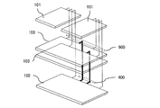
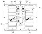
- FIG. 1 is a block diagram illustrating an example of a plurality of circuit boards and their connection relationships.
- the plurality of circuit boards 100 include a plurality of basic control units 101, a plurality of packet processing units 102, and a plurality of switch fabric units 103.
- the basic control unit 101 includes a main CPU (Central Processing Unit) 111 and a main memory 112.
- the basic control unit 101 performs device management, path information management, protocol processing, and interface control.
- the basic control unit 101 inputs and outputs control signals for the above-described control to the plurality of packet processing units 102, the plurality of switch fabric units 103, and a power supply unit described later.
- the packet processing unit 102 analyzes and transfers packets.
- the packet processing unit 102 includes a forwarding engine 121, a packet buffer 122, a header buffer 123, a search engine 124, a route search CAM (Content Address Memory) 125, an ARP (Address Resolution Protocol) search CAM 126, a filter / QoS (Quality of Service). )
- a processing CAM 127, a local switch 128, and a network interface (NIF) unit 129 are mounted.
- the switch fabric unit 103 is equipped with a crossbar switch 131.
- the crossbar switch 131 is interconnected with a local switch 128 mounted on the packet processing unit 102 via a backplane. As a result, backplane transmission is performed between the packet processing units 102 connected via the crossbar switch 131.
- the NIF unit 129 is mounted on each packet processing unit 102.
- the NIF unit 129 is an input / output port connected to a network such as a WAN (Wide Area Network) or a LAN (Local Area Network).
- the NIF unit 129 includes a line adapter 191 and a PHY (Physical Layer) chip 192.
- the PHY chip 192 performs physical layer processing such as establishment / maintenance / release of a physical connection.
- the basic control unit 101, the packet processing unit 102, and the switch fabric unit 103 are usually configured as a circuit board and are interconnected via a backplane.
- the NIF unit 129 may be configured as one element in the packet processing unit 102 or may be configured independently as a circuit board. In this example, the former configuration is employed.
- the transfer engine 121, the search engine 124, the local switch 128, the crossbar switch 131, and the like are configured as an LSI (Large Scale Integration) in which necessary functions are integrated.
- the transfer engine 121 stores data information included in the packet in the packet buffer 122 and header information in the header buffer 123.
- the header portion of the Ethernet packet includes information such as a synchronization preamble, a start frame, a reception destination and a transmission destination MAC (Media Access Control) address, and a data length.
- the search engine 124 receives header information from the transfer engine 121 and refers to various tables to acquire information necessary for packet transfer control.
- the tables referred to by the search engine 124 include a route table, an ARP table, and a filter / QoS table.
- the route table and the filter / QoS table are referred to.
- the route table is a table for performing route search processing, and is stored in the route search CAM 125.
- the filter / QoS table is information such as packet filtering conditions, discard conditions, transfer processing priority in the communication device, and the like, and is stored in the filter / QoS processing CAM 127. These search results are returned to the transfer engine 121.
- the transfer engine 121 designates an input / output port to which a packet is to be transferred from the search result, and transfers it to the local switch 128 and the crossbar switch 131 mounted on the switch fabric unit 103. Further, the crossbar switch 131 transfers the packet to the corresponding packet processing unit 102 and is sent from the local switch 128 to the transfer engine 121.
- the transfer engine 121 stores the received packet in the packet buffer 122 and the header buffer 123.
- the search engine 124 receives the header information from the transfer engine 121 and acquires the MAC address from the ARP table stored in the ARP search CAM 126.
- the ARP table is a comparison table of IP (Internet Protocol) addresses and MAC addresses used for Ethernet communication, and stores information on port numbers to which devices represented by MAC addresses are connected. This search result is returned to the transfer engine 121, and a packet is sent from the NIF unit 129 having the specified input / output port to the external interface. Thus, data transmission is performed between the plurality of circuit boards 100 in the communication device.
- IP Internet Protocol
- SerDes Serializer / Deserializer
- SerDes Serializer / Deserializer
- the backplane in the communication apparatus often performs high-speed data transmission using SerDes, which causes a problem that data cannot be received correctly on the receiving side due to high-frequency loss and intersymbol interference generated in the transmission line.
- An equalization technique is widely used as a technique for compensating for problems caused by high-frequency loss and intersymbol interference. The following two can be cited as equalization techniques.
- De-emphasis is an equalization technique that emphasizes the output voltage level of the output buffer on the data transmission side according to the frequency characteristics of transmission loss in the transmission line, and makes the signal amplitude received by the input buffer uniform.
- Equalizing is an equalization technique in which the gain characteristic of the input buffer is increased only in a specific frequency band on the data reception side in accordance with the frequency characteristic of transmission loss in the transmission line, and the signal amplitude received by the input buffer is made uniform.
- training processing is performed when the device is started up, the emphasis value of the de-emphasis circuit in the output buffer is optimized, and the gain characteristic of the amplifier circuit in the input buffer is optimized in a specific frequency band. Operation begins. Thereby, communication quality is ensured.
- the backplane interconnecting the circuit boards 100 is generally composed of a circuit board or an electric cable, but an optical cable is also adopted because the limit of electric transmission is beginning to be visible due to high-frequency loss.
- FIG. 2 is a block diagram showing another example of a plurality of circuit boards 100 and their connection relations.
- an optical device 120 connected to the local switch 128 is mounted in each packet processing unit 102.
- an optical device 130 connected to the crossbar switch 131 is mounted in each switch fabric unit 103.
- the optical device 120 of the packet processing unit 102 and the optical device 130 of the switch fabric unit 103 are connected to enable optical transmission.
- the cooling structure of the communication device on which the circuit board 100 described above is mounted is a front / rear intake / exhaust type cooling structure provided with a vent hole for passing cooling air through the backplane.
- the connection relationship of the circuit board 100 in FIG. 2 will be described as an example.
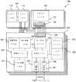
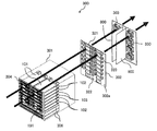
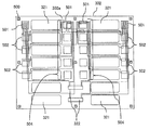
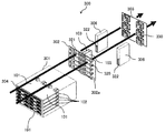
- FIG. 3 is an exploded perspective view of the communication apparatus according to the first embodiment
- FIG. 4 is a front view and a side sectional view of the communication apparatus according to the first embodiment.
- the communication device 300 includes a housing 301, a back plane 302, and a back plate 303.
- the thick arrow indicates the direction of the cooling air.
- a plurality of circuit boards 100 shown in FIG. 1 are provided in the housing 301. The plurality of circuit boards 100 are inserted in a horizontal state from the front surface of the housing 301.
- the basic control unit 101 in the first stage from the upper stage, the first stage, the third stage, the sixth stage, and the seventh stage in the packet processing unit 102, the fourth stage.
- the switch fabric unit 103 is inserted in the second and fifth stages.
- the power supply unit 306 is inserted in the eighth stage and the ninth stage (the lowest stage).
- the power supply unit 306 is also a kind of the circuit board 100.
- a front plate 304 is provided on the front surface of the housing 301.
- the front plate 304 has a mesh-shaped vent 305 that allows cooling air to pass through the housing 301. Thereby, cooling air is sucked into the housing 301 from the front plate 304. Further, the line adapter 191 of each circuit board 100 is exposed on the front plate 304. As a result, the external interface and the line adapter 191 can be connected while passing cooling air.
- the backplane 302 is a substrate (connection plate) for connecting a plurality of circuit boards 100.
- a plurality of connectors 320 are provided on the front surface 302 a that is one surface of the backplane 302, and each connector 320 is connected to each circuit board 100.
- a plurality of vent holes 321 are formed in the back plane 302.
- Each circuit board 100 connected to the backplane 302 is disposed so as to block a part of the corresponding vent 321. In order to allow the cooling air to pass, each circuit board 100 does not block all the corresponding vent holes 321.
- the cooling air passing through the circuit board 100 passes through the vent 321.
- the cable 400 that electrically or optically connects the circuit boards 100 is routed and connected to the rear surface 302b side that is the other surface via the connector 320. Thereby, signal transmission and power feeding between the circuit boards 100 are executed.
- the number of circuit boards 100 to be mounted is not limited to the number in FIG.
- a plurality of power supply units 306 are inserted into the housing 301, and redundancy of the communication device 300 is realized.
- the plurality of power supply units 306 are inserted horizontally from the front surface of the communication device 300.
- AC 100 [V] or AC 200 [V] is often used for AC machines
- DC 48 [V] is often used for DC machines, and these are applied to the power supply unit 306.
- the power supply unit 306 outputs DC48 [V] or DC12 [V] by AC / DC conversion processing or DC / DC conversion processing.
- the power supply unit 306 is connected to the backplane 302 by a power supply unit connector 322 which is an example of the connector 320, and DC48 [V] or DC12 [V] is supplied to each circuit board 100 via the backplane 302. Note that the number of power supply units 306 mounted is not limited to the number shown in FIG.
- a plurality of cooling fans 330 are mounted on the back plate 303.
- the cooling fan 330 is provided along the circuit board stacking direction. With the cooling fan 330, the communication device 300 forcibly sucks the cooling air from the front plate 304 of the communication device 300 and exhausts the cooling air that has passed through the circuit board 100 and the vent 321.
- the number of mounted cooling fans 330 is not limited to the number shown in the figure.
- the backplane 302 includes a space inside the housing 301, a first space on the front surface 302a side to which the plurality of circuit boards 100 are connected, and a second space on the rear surface 302b side in which the cable 400 is routed. Divided into space. The first space and the second space are communicated with each other through a vent 321. In addition, the cable 400 is routed in a fourth space of the second space excluding the third space in which the vent 321 is projected on the rear surface 302b in the cooling air flow direction.
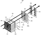
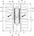
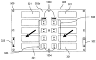
- FIG. 5 is a front view of the backplane 302 according to the first embodiment
- FIG. 6 is a rear view of the backplane 302 according to the first embodiment.
- the thick arrow indicates the wind direction.
- the back plane 302 has nine screw holes 500 for fixing to the housing 301 on the front surface 302a as a front surface, two rows and eighteen vent holes 321, a control signal connector 501 of the basic control unit 101, packet processing.
- the unit 102 includes a control signal connector 502, a switch fabric unit 103 control signal connector 503, a power supply unit connector 322, and a high-speed signal connector 504.
- a line connecting the connectors 320 (501 to 504) is a signal line laid on the backplane 302. This signal line transmits a signal for performing relatively low-speed data transmission such as a control signal.
- a signal for performing high-speed data transmission is transmitted by the cable 400 routed to the rear surface 302b side which is the back surface.
- the control signal connectors 501 to 503 and the high-speed signal connector 504 are arranged separately on the front surface 302a with the vent 321 interposed therebetween.
- the backplane 302 has a high-speed signal orthogonal connector 604 on the rear surface 302b.
- Each high-speed signal orthogonal type connector 604 is connected to a high-speed signal connector 504 on the front surface 302a directly behind.
- the high-speed signal orthogonal connector 604 is connected by a cable 400 that is electrically or optically connected.
- the cable 400 is arranged so as not to overlap with the vent 321 when viewed from the front surface 302a. That is, the cable 400 is arranged on the rear surface 302b so as not to protrude from the region of the rear surface 302b excluding the vent hole 321.
- the cooling air from the front surface of the housing 301 does not easily hit the cable 400, the passage of the cooling air is not hindered.
- the shaking of the cable 400 is suppressed. Therefore, when the cable 400 is an electric cable, contact failure and electrical resistance are suppressed, and malfunction can be suppressed. Further, when the cable 400 is an optical cable, it is possible to reduce a loss due to an optical axis shift or a connection angle shift.
- a fixing member 601 is used as an example of the swing suppression unit of the cable 400.
- the fixing member 601 fixes the cable 400 to the rear surface 302b.
- the fixing member 601 may bundle a plurality of cables 400 and fix them to the rear surface 302b.
- a shielding plate 800 may be used as another example of the swing suppression means of the cable 400.
- the shielding plate 800 is provided on the surface on which the cooling fan 330 of the back plate 303 shown in FIG. 3 is mounted.
- the shielding plate 800 is orthogonal to the plate surface of the back plate 303.
- the two shielding plates 800 are provided between the cable 400 connected to the backplane 302 and the vent 321 and shield the cable 400 from the cooling air. Note that both the shielding plate 800 and the fixing member 601 may be provided, or at least one may be provided.
- the cable 400 is not subjected to cooling air, so that the shaking of the cable 400 is suppressed. Therefore, when the cable 400 is an electric cable, contact failure and electrical resistance are suppressed, and malfunction can be suppressed. Further, when the cable 400 is an optical cable, it is possible to reduce a loss due to an optical axis shift or a connection angle shift.
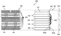
- FIG. 7 is a side view showing the fixing member 601 and the cable 400 fixed by the fixing member 601.
- the cable 400 that connects between the high-speed signal orthogonal connectors 604 has its midway portion 700 bent to the rear surface 302 b side and fixed by a fixing member 601.
- the bending radius R of the cable 400 is not less than a predetermined bending radius.
- the predetermined bending radius is the minimum value of the bending radius that does not deteriorate the communication quality of the cable 400.
- the bending radius R is preferably 5 to 10 times in the case of the electric cable 400 and 10 to 20 times in the case of the optical cable 400 with respect to the outer diameter D of the cable 400.
- the bending radius of the cable 400 can be kept moderate, and the cable 400 can be prevented from being damaged or deteriorated in characteristics. Accordingly, it is possible to employ a cable arrangement that is not affected by the cooling air while adopting a front-rear intake / exhaust cooling structure, and to improve the signal transmission speed.
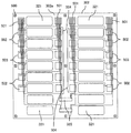
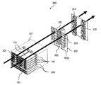
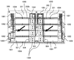
- FIG. 8 is an exploded perspective view of the communication device 300 when another example of the means for suppressing the swing of the cable 400 is employed.
- a shielding plate 800 is employed as another example of the swing suppression means.
- the shielding plate 800 is provided on the surface of the back plate 303 on which the cooling fan 330 is mounted.
- the shielding plate 800 is orthogonal to the plate surface of the back plate 303.
- the two shielding plates 800 are provided between the cable 400 connected to the backplane 302 and the vent 321 and shield the cable 400 from the cooling air.
- the cable 400 is not subjected to cooling air, so that the shaking of the cable 400 is suppressed. Therefore, when the cable 400 is an electric cable, contact failure and electrical resistance are suppressed, and malfunction can be suppressed. Further, when the cable 400 is an optical cable, it is possible to reduce a loss due to an optical axis shift or a connection angle shift.
- FIG. 9 is an explanatory diagram three-dimensionally showing the connection relationship between the circuit boards 100 according to the first modification.
- the packet processing unit 102 is described as one sheet for simplicity of explanation.
- Two basic control units 101 are mounted. Each basic control unit 101 is connected to the packet processing unit 102 and the switch fabric unit 103 by a cable 900.
- the control signal from the basic control unit 101 is often a relatively low speed signal.
- the packet processing unit 102 and the switch fabric unit 103 are parts that require particularly high throughput in the communication apparatus 300, and are connected by a cable 400 using SerDes.
- no signal line is laid on the front surface 302a that is the front surface of the backplane 302 according to the first modification.
- Other configurations are the same as those in FIG.
- FIG. 10 is a rear view of the backplane 302 according to the first modification.
- a high-speed signal orthogonal connector 604 and control signal rear-side connectors 1001 to 1003 are provided on the rear surface 302b which is the back surface of the backplane 302.
- the high-speed signal orthogonal connector 604 is connected by a cable 400 (hereinafter, referred to as a first cable 400), as in the first embodiment.
- control signal rear connectors 1001 to 1003 are provided.
- the control signal rear side connectors 1001 to 1003 are connected by a cable 1000 (hereinafter referred to as a second cable 1000) that performs relatively low-speed data transmission.
- the second cable 1000 is also arranged so as not to overlap with the vent 321 when viewed from the front surface 302a. That is, the second cable 1000 is arranged on the rear surface 302b so as not to protrude from the region of the rear surface 302b excluding the vent hole 321.
- a fixing member 1004 is used as an example of the swing suppression means of the second cable 1000.
- the fixing member 1004 fixes the second cable 1000 to the rear surface 302b.
- the fixing member 1004 may bundle a plurality of second cables 1000 and fix them to the rear surface 302b.
- the control signal data transmission is performed by the second cable 1000, so that the backplane 302 has no wiring pattern and only the power supply layer to each circuit board 100. It becomes the provided substrate. Therefore, the manufacturing cost can be suppressed, and the inexpensive backplane 302 can be provided accordingly.
- the cooling air from the front surface of the housing 301 is difficult to hit the cable 400, the passage of the cooling air is not hindered. Moreover, since it becomes difficult for the cooling air to hit, the shaking of the cable 400 is suppressed. Therefore, when the cable 400 is an electric cable, contact failure and electrical resistance are suppressed, and malfunction can be suppressed. Further, when the cable 400 is an optical cable, it is possible to reduce a loss due to an optical axis shift or a connection angle shift.
- the switch fabric unit 103 is inserted on the front surface 302a side of the backplane 302.
- the switch fabric unit 103 is provided on the rear surface 302b side of the backplane 302.
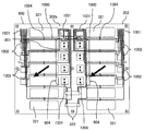
- FIG. 11 is an exploded perspective view of the communication device 300 according to the second modification.
- the communication device 300 includes a housing 301, a back plane 302, and a back plate 303.
- a plurality of circuit boards 100 are provided in the housing 301.
- the plurality of circuit boards 100 are inserted in a horizontal state from the front surface of the housing 301.
- the basic control unit 101 is in the first stage from the top
- the packet processing unit 102 is in the first to fifth stages
- the power supply unit 306 is in the sixth and seventh stages (bottom stage). Is inserted.
- the switch fabric unit 103 is inserted on the rear surface 302b side of the backplane 302.
- the switch fabric unit 103 is inserted at a right angle to the other circuit board 100.
- the switch fabric unit 103 is inserted at a position where the vent hole 321 is not blocked.
- the basic control unit 101, the packet processing unit 102, and the switch fabric unit 103 are connected via a connector with the backplane 302 interposed therebetween.
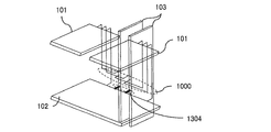
- FIG. 12 is a front view of the backplane 302 according to the second modification
- FIG. 13 is a rear view of the backplane 302 according to the second modification.
- the control signal connector 503 of the switch fabric unit 103 is not provided on the front surface 302a which is the front surface.
- a high-speed signal orthogonal connector 604 is used for connection of signals for high-speed data transmission.
- the circuit board (packet processing unit 102) on the front surface 302a side and the circuit board (switch fabric unit 103) on the rear surface 302b side through the through-hole 1304 of the backplane 302, without using signal lines or cables on the circuit board. are connected directly.
- the switch fabric unit 103 is connected from the rear surface 302b side of the back plane 302 by a control signal rear surface connector 1003.
- Other configurations are the same as those in FIG. 5 of the first embodiment.
- 103 is connected through a through hole 1304 of the backplane 302. Therefore, the signal transmission speed can be improved.
- the cable 400 does not exist as in the first embodiment, the cable 400 is not swung by the cooling air. Therefore, there is no loss due to poor contact, electrical resistance, optical axis deviation, or connection angle deviation.
- Modification 3 has a structure in which Modification 1 is applied to Modification 2.
- a signal for performing low-speed data transmission such as a control signal is transmitted through a signal line laid on the backplane 302
- the second signal is also transmitted for the signal. Data transmission through the cable 1000 is performed.
- FIG. 14 is an explanatory diagram three-dimensionally showing the connection relationship between the circuit boards 100 according to the third modification.
- the packet processing unit 102 is described as one sheet for the sake of simplicity.
- Two basic control units 101 are mounted. Each basic control unit 101 is connected to the packet processing unit 102 and the switch fabric unit 103 by the second cable 1000.
- the control signal from the basic control unit 101 is often a relatively low speed signal.
- the packet processing unit 102 and the switch fabric unit 103 are parts that require a particularly high throughput in the communication device 300 and are connected via a through hole 1304 of the backplane 302.
- the communication apparatus 300 according to the second modification can shorten the cable length of the second cable 1000.
- the two-stage switch fabric unit 103 is not inserted from the front surface of the housing 301. Thereby, the height of the housing 301 can be reduced, and the communication device 300 can be reduced in size.
- FIG. 15 is a rear view of the backplane 302 according to the third modification.
- a high-speed signal orthogonal connector 604 and control signal rear-side connectors 1001 and 1002 are provided on the rear surface 302 b which is the back surface of the backplane 302.
- the high-speed signal orthogonal connector 604 is directly connected to the circuit board on the front surface 302a side and the circuit board on the rear surface 302b side through the through-hole 1304 of the backplane 302.
- control signal rear connectors 1001 and 1002 are provided.
- the control signal rear side connectors 1001 and 1002 are connected by a cable 1000 that performs relatively low-speed data transmission.
- the cable 1000 is arranged so as not to overlap with the vent 321 when viewed from the front surface 302a. That is, the cable 1000 is arranged on the rear surface 302b so as not to protrude from the region of the rear surface 302b excluding the vent 321.
- a fixing member 1004 is used as an example of means for suppressing the swing of the cable 1000.
- the fixing member 1004 fixes the cable 1000 to the rear surface 302b.
- the fixing member 1004 may bundle a plurality of cables 1000 and fix them to the rear surface 302b.
- the backplane 302 has no wiring pattern and is provided with only a power supply layer for each circuit board unit by adopting a configuration in which the data transmission of the control signal is performed by the cable 1000. It becomes. Therefore, the manufacturing cost can be suppressed, and the inexpensive backplane 302 can be provided accordingly.
- the cable 400 since the cable 400 does not exist as in the second modification, the cable 400 does not swing due to the cooling air. Therefore, there is no loss due to poor contact, electrical resistance, optical axis deviation, or connection angle deviation.
- the modification 4 is a structure in which the arrangement of the power supply unit 306 is changed in the structure of the modification 2.
- the power supply unit 306 is inserted on the front surface 302a side of the backplane 302, but in Modification 4, the power supply unit 306 is provided along with the switch fabric unit 103 on the rear surface 302b side of the backplane 302. Accordingly, the space in the housing 301 is effectively used, and the height at which the circuit board 100 is loaded becomes shorter as the power supply unit 306 is removed, so that the height of the housing 301 can be kept low. Therefore, the communication device 300 can be reduced in size.
- FIG. 16 is an exploded perspective view of the communication device 300 according to the fourth modification.
- the communication device 300 includes a housing 301, a back plane 302, and a back plate 303.
- a plurality of circuit boards 100 are provided in the housing 301.
- the plurality of circuit boards 100 are inserted in a horizontal state from the front surface of the housing 301.
- the basic processing unit 101 is inserted in the first stage from the upper stage, and the packet processing unit 102 is inserted in the second to fifth stages (lowermost stage) in the casing 301.
- the switch fabric unit 103 is arranged at the same position as in FIG.
- the power supply unit 306 is inserted on the rear surface 302b side of the back plane 302.
- the power supply unit 306 is inserted at right angles to the other circuit board 100 on the front surface 302a side.
- the power supply unit 306 is inserted at a position where the vent 321 is not blocked.
- the power supply unit 306 is connected to the backplane 302 from the rear surface 302b side by a power supply unit connector 322.
- the other configuration of the power supply unit 306 is the same as that of the above-described embodiment.
- the backplane 302 according to the modified example 4 has a high-speed signal connector 504 disposed at the position of the power supply unit connector 322 on the front surface 302a as a front surface, unlike FIG. Further, unlike FIG. 12, the control signal connector 502 of the packet processing unit 102 is disposed on the opposite side of the vent hole from the side where the high-speed signal connector 504 is disposed.
- Other configurations are the same as those in FIG.
- Modification 4 the power supply unit 306 is disposed on the rear surface 302b side of the backplane 302. For this reason, the height of the housing 301 is shortened, and the vent hole 321 for the power supply unit 306 is not necessary, and the height of the backplane 302 is shortened accordingly. Thereby, size reduction of the communication apparatus 300 is implement
- FIG. 17 is a rear view of the backplane 302 according to the fourth modification.
- the modification 2 differs from FIG. 13 in that, in the modification 4, the power unit 306 is disposed on the rear surface 302b side of the backplane 302 in FIG. It is a point mounted on 302b.
- the power supply unit 306 is disposed on both left and right edges of the rear surface 302b of the backplane 302 that do not overlap with the vent holes 321. Therefore, since the power supply unit 306 does not shield the vent 321, it is possible to prevent the cooling efficiency from being reduced.
- the front-side 302a-side circuit board and the rear-side 302b-side circuit board that perform high-speed data transmission are directly connected to each other while adopting the front-rear intake / exhaust cooling structure. . Therefore, the signal transmission speed can be improved. Further, since the power supply unit 306 is disposed on the rear surface 302b side of the backplane 302, the height at which the circuit boards are stacked can be shortened, and the communication device 300 can be downsized.
- Modification 5 has a structure in which Modification 1 is applied to Modification 4.
- Modification 4 an example in which a signal for performing low-speed data transmission such as a control signal is transmitted through a signal line laid on the backplane 302 has been described.
- the signal is also transmitted via a cable. Perform transmission.
- a signal line is not laid on the front surface 302a which is the front surface of the backplane according to the fifth modification. Others are the front surface of the structure similar to the modification 4.
- FIG. 18 is a rear view of the backplane 302 according to the fifth modification.
- a high-speed signal orthogonal connector 604 a control signal rear connector 1002, and a power feeding rear connector 1800 are provided on the rear surface 302 b which is the back surface of the back plane 302.
- the high-speed signal orthogonal connector 604 is directly connected to the circuit board 100 on the front surface 302 a side and the circuit board 100 on the rear surface 302 b side through the through holes 1304 of the backplane 302.
- a control signal rear connector 1002 is provided.
- the control signal rear connector 1002 is connected by a cable 1000 that performs relatively low-speed data transmission.
- the cable 1000 is also arranged so as not to overlap with the vent 321 when viewed from the front surface 302a. That is, the cable 1000 is arranged on the rear surface 302b so as not to protrude from the region of the rear surface 302b excluding the vent 321.
- a power supply rear side connector 1800 is provided.
- the power supply rear side connector 1800 and the control signal rear side connector 1001 are connected by a power control cable 1801.
- the cable 1801 is also arranged so as not to overlap with the vent 321 when viewed from the front surface 302a. That is, the cable 1801 is arranged on the rear surface 302b so as not to protrude from the region of the rear surface 302b excluding the vent hole 321.
- a fixing member 1004 is used as an example of a swing suppression unit for the cables 1000 and 1801.
- the fixing member 1004 fixes the cables 1000 and 1801 to the rear surface 302b.
- the fixing member 1004 may bundle a plurality of cables 1000 and 1801 and fix them to the rear surface 302b.
- the backplane 302 has no wiring pattern and is connected to each circuit board 100 by performing control signal data transmission with the cable 1000 and power supply control with the cable 1801.
- the substrate provided with only the power feeding layer. Therefore, the manufacturing cost can be suppressed, and the inexpensive backplane 302 can be provided accordingly.
- the communication device According to the communication device according to the present embodiment, there is a concern when the cable is shaken by cooling air and malfunctions due to poor contact or increased electrical resistance when connected by an electric cable. In addition, it is possible to reduce the influence of an increase in loss due to an optical axis shift or a connection angle shift when connected by an optical cable. In addition, it is possible to maintain a gentle bending radius that prevents damage to the cable and deterioration of characteristics, and it is possible to improve the signal transmission speed.
- the wiring layer including the signal line laid on the backplane is eliminated, and the backplane is provided with only a power feeding layer for each circuit board, thereby reducing the manufacturing cost of the backplane. Can do.
- the cooling air is sucked from the mesh-like vent 305 on the front surface of the communication device 300 and exhausted to the rear surface of the communication device through the vent 321 of the backplane 302.
- the cooling fan 330 may be a push-type cooling fan so that air is sucked from the rear surface of the communication device 300 and exhausted to the front surface of the communication device 300.
- the power supply unit 306 is inserted horizontally from the front surface of the communication device 300, but may be inserted horizontally from the rear surface of the communication device 300. Further, in Modification 4 and Modification 5, the power supply unit 306 is inserted vertically from the rear surface of the communication device 300, but may be inserted vertically from the front surface of the communication device 300.
- the cooling fan 330 may not be mounted on the communication device 300 but may be disposed behind the back plate 303 outside the communication device 300. Good. Thereby, size reduction of the communication apparatus 300 can be achieved.
- a plurality of communication devices 300 described above may be arranged.
- the communication devices 300 are arranged in a direction orthogonal to the cooling air flow direction.
- the communication device 300 is arranged vertically or horizontally. Accordingly, any communication device 300 can be cooled without sucking the cooling air exhausted from the other communication devices 300.
- a communication device is assumed, but the present invention can be applied to an information processing device such as a server without departing from the gist of the present invention.
Landscapes
- Engineering & Computer Science (AREA)
- Theoretical Computer Science (AREA)
- Physics & Mathematics (AREA)
- General Engineering & Computer Science (AREA)
- General Physics & Mathematics (AREA)
- Microelectronics & Electronic Packaging (AREA)
- Computer Hardware Design (AREA)
- Human Computer Interaction (AREA)
- Aviation & Aerospace Engineering (AREA)
- Thermal Sciences (AREA)
- Mathematical Physics (AREA)
- Mounting Of Printed Circuit Boards And The Like (AREA)
- Cooling Or The Like Of Electrical Apparatus (AREA)
Priority Applications (1)
| Application Number | Priority Date | Filing Date | Title |
|---|---|---|---|
| US14/760,504 US20150355690A1 (en) | 2013-03-14 | 2013-09-03 | Communication apparatus |
Applications Claiming Priority (2)
| Application Number | Priority Date | Filing Date | Title |
|---|---|---|---|
| JP2013052277A JP5926212B2 (ja) | 2013-03-14 | 2013-03-14 | 通信装置 |
| JP2013-052277 | 2013-03-14 |
Publications (1)
| Publication Number | Publication Date |
|---|---|
| WO2014141503A1 true WO2014141503A1 (ja) | 2014-09-18 |
Family
ID=51536192
Family Applications (1)
| Application Number | Title | Priority Date | Filing Date |
|---|---|---|---|
| PCT/JP2013/073692 Ceased WO2014141503A1 (ja) | 2013-03-14 | 2013-09-03 | 通信装置 |
Country Status (3)
| Country | Link |
|---|---|
| US (1) | US20150355690A1 (enExample) |
| JP (1) | JP5926212B2 (enExample) |
| WO (1) | WO2014141503A1 (enExample) |
Families Citing this family (5)
| Publication number | Priority date | Publication date | Assignee | Title |
|---|---|---|---|---|
| WO2015087418A1 (ja) * | 2013-12-11 | 2015-06-18 | 株式会社日立製作所 | 記憶制御装置の冷却機構 |
| JP6422845B2 (ja) * | 2015-11-12 | 2018-11-14 | アラクサラネットワークス株式会社 | 通信装置 |
| US10517189B1 (en) * | 2018-08-27 | 2019-12-24 | Quanta Computer Inc. | Application and integration of a cableless server system |
| CN114650702A (zh) * | 2020-12-17 | 2022-06-21 | 华为技术有限公司 | 阵列式连接结构及电子设备 |
| US20250008675A1 (en) * | 2023-06-29 | 2025-01-02 | Integrotech Sp. Z O.O. | Modular device enabling flexible expansion of the functions of monitoring, configuring, regulating, measuring and archiving parameters of the gas and liquid media transmission process for calculators/convertors |
Citations (3)
| Publication number | Priority date | Publication date | Assignee | Title |
|---|---|---|---|---|
| US7722359B1 (en) * | 2007-09-27 | 2010-05-25 | Emc Corporation | Connection assembly having midplane with enhanced connection and airflow features |
| JP2011146470A (ja) * | 2010-01-13 | 2011-07-28 | Alaxala Networks Corp | 電子装置 |
| JP2012109363A (ja) * | 2010-11-17 | 2012-06-07 | Alaxala Networks Corp | 電子装置 |
Family Cites Families (29)
| Publication number | Priority date | Publication date | Assignee | Title |
|---|---|---|---|---|
| US4055973A (en) * | 1976-03-11 | 1977-11-01 | Best Walter E | Equipment lock |
| US4103453A (en) * | 1977-02-01 | 1978-08-01 | Robert Michael Baron | Adjustable U-control handle |
| JPH06140776A (ja) * | 1992-10-28 | 1994-05-20 | Ricoh Co Ltd | 電子装置 |
| US6728099B1 (en) * | 1998-11-13 | 2004-04-27 | Hewlett-Packard Development Company, L.P. | Electrical component having a hybrid air cooling system and method |
| US6816486B1 (en) * | 1999-03-25 | 2004-11-09 | Inrange Technologies Corporation | Cross-midplane switch topology |
| US6422876B1 (en) * | 1999-12-08 | 2002-07-23 | Nortel Networks Limited | High throughput interconnection system using orthogonal connectors |
| US6411506B1 (en) * | 2000-07-20 | 2002-06-25 | Rlx Technologies, Inc. | High density web server chassis system and method |
| US6723915B2 (en) * | 2001-12-14 | 2004-04-20 | Sun Microsystems, Inc. | Emi-shielding riser card for a computer chassis |
| US20040094328A1 (en) * | 2002-11-16 | 2004-05-20 | Fjelstad Joseph C. | Cabled signaling system and components thereof |
| US8338713B2 (en) * | 2002-11-16 | 2012-12-25 | Samsung Electronics Co., Ltd. | Cabled signaling system and components thereof |
| US6927975B2 (en) * | 2003-06-27 | 2005-08-09 | International Business Machines Corporation | Server blade modular chassis mechanical and thermal design |
| US6966784B2 (en) * | 2003-12-19 | 2005-11-22 | Palo Alto Research Center Incorporated | Flexible cable interconnect assembly |
| US20050207134A1 (en) * | 2004-03-16 | 2005-09-22 | Belady Christian L | Cell board interconnection architecture |
| US7094102B2 (en) * | 2004-07-01 | 2006-08-22 | Amphenol Corporation | Differential electrical connector assembly |
| US7280356B2 (en) * | 2004-12-14 | 2007-10-09 | Amphenol Corporation | Air cooling architecture for orthogonal board architectures |
| DE112005003506T5 (de) * | 2005-03-28 | 2008-02-21 | Fujitsu Ltd. | Elektronische Vorrichtung |
| JP2007011931A (ja) * | 2005-07-04 | 2007-01-18 | Hitachi Ltd | 記憶制御装置 |
| JP4858750B2 (ja) * | 2005-10-06 | 2012-01-18 | 日本電気株式会社 | 情報処理装置 |
| US7295446B2 (en) * | 2005-12-30 | 2007-11-13 | International Business Machines Corporation | Midplane connector for blades |
| US8764527B2 (en) * | 2006-02-10 | 2014-07-01 | Schneider Electric It Corporation | Method and apparatus for providing cooling air to equipment |
| US20070232089A1 (en) * | 2006-03-31 | 2007-10-04 | Nortel Networks Limited | Bridge modules for connecting plural groups of electronic modules |
| US20070293137A1 (en) * | 2006-06-20 | 2007-12-20 | International Business Machines Corporation | Acoustic noise reduction using airflow management |
| US7890677B2 (en) * | 2006-09-13 | 2011-02-15 | Dell Products L.P. | Chassis management access console via a local KVM display |
| US20090016019A1 (en) * | 2007-07-13 | 2009-01-15 | International Business Machines Corporation | Airflow control and dust removal for electronic systems |
| US7974105B2 (en) * | 2008-01-07 | 2011-07-05 | Chatsworth Products, Inc. | Apparatus and method for organizing cables in a cabinet |
| US8064200B1 (en) * | 2008-04-16 | 2011-11-22 | Cyan Optics, Inc. | Cooling a chassis by moving air through a midplane between two sets of channels oriented laterally relative to one another |
| US9019708B2 (en) * | 2011-08-25 | 2015-04-28 | Lsi Corporation | Apparatus and systems having storage devices in a side accessible drive sled |
| CN203423892U (zh) * | 2013-05-23 | 2014-02-05 | 杭州华三通信技术有限公司 | 电子设备 |
| JP6485193B2 (ja) * | 2015-04-30 | 2019-03-20 | 富士通株式会社 | 電子機器収納装置および中継装置 |
-
2013
- 2013-03-14 JP JP2013052277A patent/JP5926212B2/ja not_active Expired - Fee Related
- 2013-09-03 US US14/760,504 patent/US20150355690A1/en not_active Abandoned
- 2013-09-03 WO PCT/JP2013/073692 patent/WO2014141503A1/ja not_active Ceased
Patent Citations (3)
| Publication number | Priority date | Publication date | Assignee | Title |
|---|---|---|---|---|
| US7722359B1 (en) * | 2007-09-27 | 2010-05-25 | Emc Corporation | Connection assembly having midplane with enhanced connection and airflow features |
| JP2011146470A (ja) * | 2010-01-13 | 2011-07-28 | Alaxala Networks Corp | 電子装置 |
| JP2012109363A (ja) * | 2010-11-17 | 2012-06-07 | Alaxala Networks Corp | 電子装置 |
Also Published As
| Publication number | Publication date |
|---|---|
| JP2014179454A (ja) | 2014-09-25 |
| JP5926212B2 (ja) | 2016-05-25 |
| US20150355690A1 (en) | 2015-12-10 |
Similar Documents
| Publication | Publication Date | Title |
|---|---|---|
| JP5926212B2 (ja) | 通信装置 | |
| US7804840B2 (en) | Combined FCoE network device | |
| US11206225B2 (en) | Hyperscale switch and method for data packet network switching | |
| CN104982018B (zh) | 将高速多通道链路中的通道与互连之间的训练模式序列解相关 | |
| US20040003141A1 (en) | System and method for implementing virtual adapters and virtual interfaces in a network system | |
| US20030208633A1 (en) | System and method for implementing LAN within shared I/O subsystem | |
| JP6605747B2 (ja) | ラインカードシャーシ、マルチシャーシクラスタルータおよびパケット処理 | |
| US10331598B2 (en) | Adding a network port to a network interface card | |
| US11057316B2 (en) | Lite network switch architecture | |
| JP6037021B2 (ja) | 通信装置及び通信システム | |
| JP6422845B2 (ja) | 通信装置 | |
| US8208480B2 (en) | Stackable network processing device with top mounted IO port connectors | |
| JP5966488B2 (ja) | ネットワークシステム、スイッチ、及び通信遅延短縮方法 | |
| US8135012B2 (en) | Redundant routing of data in a network | |
| WO2015081506A1 (zh) | 用于通信设备的互连系统 | |
| US8396005B2 (en) | High-speed IP flow mediation apparatus using network processor | |
| US6998734B1 (en) | Systems and methods for providing high density connections for a network device | |
| CN220798315U (zh) | 一种网络地址转换装置 | |
| US7366167B2 (en) | Apparatus and method for hairpinning data packets in an Ethernet MAC chip | |
| EP3987733B1 (en) | Method and apparatus for reconfigurable network device | |
| US11218401B2 (en) | Computer network device, a computer internetwork and a method for computer networking | |
| Premod et al. | Network design for submarine sonar systems | |
| CN119155882A (zh) | 单板、单板的组装方法和通信设备 |
Legal Events
| Date | Code | Title | Description |
|---|---|---|---|
| 121 | Ep: the epo has been informed by wipo that ep was designated in this application |
Ref document number: 13878407 Country of ref document: EP Kind code of ref document: A1 |
|
| WWE | Wipo information: entry into national phase |
Ref document number: 14760504 Country of ref document: US |
|
| NENP | Non-entry into the national phase |
Ref country code: DE |
|
| 122 | Ep: pct application non-entry in european phase |
Ref document number: 13878407 Country of ref document: EP Kind code of ref document: A1 |