WO2014141398A1 - Pwm control method and power conversion apparatus using same - Google Patents
Pwm control method and power conversion apparatus using same Download PDFInfo
- Publication number
- WO2014141398A1 WO2014141398A1 PCT/JP2013/056906 JP2013056906W WO2014141398A1 WO 2014141398 A1 WO2014141398 A1 WO 2014141398A1 JP 2013056906 W JP2013056906 W JP 2013056906W WO 2014141398 A1 WO2014141398 A1 WO 2014141398A1
- Authority
- WO
- WIPO (PCT)
- Prior art keywords
- voltage
- phase
- modulation factor
- output
- inverter circuit
- Prior art date
Links
Images


Classifications
-
- H—ELECTRICITY
- H02—GENERATION; CONVERSION OR DISTRIBUTION OF ELECTRIC POWER
- H02M—APPARATUS FOR CONVERSION BETWEEN AC AND AC, BETWEEN AC AND DC, OR BETWEEN DC AND DC, AND FOR USE WITH MAINS OR SIMILAR POWER SUPPLY SYSTEMS; CONVERSION OF DC OR AC INPUT POWER INTO SURGE OUTPUT POWER; CONTROL OR REGULATION THEREOF
- H02M7/00—Conversion of ac power input into dc power output; Conversion of dc power input into ac power output
- H02M7/42—Conversion of dc power input into ac power output without possibility of reversal
- H02M7/44—Conversion of dc power input into ac power output without possibility of reversal by static converters
- H02M7/48—Conversion of dc power input into ac power output without possibility of reversal by static converters using discharge tubes with control electrode or semiconductor devices with control electrode
- H02M7/483—Converters with outputs that each can have more than two voltages levels
- H02M7/487—Neutral point clamped inverters
Definitions
- the present invention relates to a PWM (Pulse Width Modulation) control method (control method) of a three-level inverter that converts a DC voltage into a three-phase AC voltage, and a power converter using the same.
- PWM Pulse Width Modulation
- PWM control inverter device power converter using PWM control method
- DC voltage (current) into three-phase AC voltage (current) is motor control, uninterruptible power supply, power conditioner, frequency power converter It is used for such as.
- a triangular wave comparison method sub-harmonic method
- a triangular wave comparison method a triangular wave carrier signal and a sinusoidal voltage command are compared.
- the transistor connected to the high voltage node is turned on, and when the voltage command is low, the low voltage node is set. Turn on the connected transistor.
- a phase voltage corresponding to a three-phase sine wave is obtained.
- the PWM control inverter device there are a two-level inverter and a three-level inverter.
- a two-level inverter which is a typical inverter, inputs a DC voltage + Ed, -Ed to an inverter main circuit, and is positive (+ Ed), negative (-Ed) by a leg circuit composed of two transistors per output phase.
- a three-level inverter inputs a DC voltage + Ed, -Ed and a zero potential obtained by dividing into two by a capacitor to the inverter main circuit, and a leg circuit composed of four transistors per output phase.
- the inverter can output three-stage PWM voltage waveforms of positive (+ Ed), negative ( ⁇ Ed), and 0. Since the change rate of the output voltage due to switching is halved in the 3-level inverter compared to the 2-level inverter, switching is performed by halving the switching voltage of the switch elements constituting the inverter main circuit. Loss can be reduced.
- a two-phase modulation method as a PWM control method for reducing switching loss by stopping transistor switching for a certain period and reducing the number of times the inverter main circuit is switched.
- a zero-phase component signal is added to each phase so that the voltage command given to one phase switching element (switching device) of the three phases becomes the maximum value or the minimum value of the triangular wave carrier. Is fixed to an ON or OFF state for a predetermined period.
- the switching loss of the transistor can be reduced without changing the line voltage of the fundamental wave component.
- the voltage mode is switched every 60 degrees with respect to the phase angle of the output frequency, and control is performed so that each phase is always in an ON or OFF state in order.
- the voltage utilization rate can be increased because the sinusoidal shape of the line voltage is not distorted. It also has features. Note that “3 1/2 ” is the route 3, but is simply simplified as “ ⁇ 3”.
- Patent Document 1 A technique in which a two-phase modulation method is applied to a two-level inverter is disclosed in Patent Document 1. Further, as in the two-phase modulation method, a technique in which a PWM control method for stopping switching of a transistor for a certain period is applied to a three-level inverter is disclosed in Patent Document 2.
- the two-phase modulation method since the two-phase modulation method includes many harmonics in the output phase voltage, it causes harmonic noise. This harmonic also causes a further increase in power loss such as a ground capacitor.
- the modulation factor is high (close to 2 / ⁇ 3), the output voltage jump voltage width and harmonics are small, but when the modulation factor is low, the output voltage jump voltage width, Since the harmonics become large, the adverse effects caused by the zero-phase current and the harmonics become large.
- the present invention solves such problems, and its object is to achieve power loss due to zero-phase voltage (current) of the inverter to which the two-phase modulation method is applied, harmonic noise, and peripheral devices. It is providing the PWM control method which reduces the bad influence on a power converter, and a power converter device using the same.
- the present invention is configured as follows. That is, the PWM control method of the present invention generates a pulse for controlling the switch of the inverter circuit by comparing the first, second and third voltage commands with the carrier triangular wave, and the first, second and third Are obtained by adding a zero-phase signal to the first, second, and third basic sine waves, respectively, and the first, second, and third basic sine waves are 0 to 2 / ⁇ .
- the zero-phase signal is a value obtained by selecting a median value from (1 ⁇ Va), (Va + Vb), and ( ⁇ 1 ⁇ Vb).
- the power conversion device of the present invention includes an inverter circuit composed of a plurality of switching devices that output DC voltage waveforms of three stages of + Ed, 0, and ⁇ Ed using DC voltages + Ed and ⁇ Ed as power sources, And a control circuit for generating a PWM voltage waveform from the output of the inverter circuit, the control circuit being proportional to a predetermined modulation factor M, The amplitude of the frequency component is controlled, and the output voltage of the inverter circuit is set to any one of + Ed, 0, and -Ed with respect to a specific phase angle range of the fundamental frequency component during one period of the fundamental frequency component.
- the output voltage of the inverter circuit is set to + Ed, 0, and ⁇ Ed in the specific phase angle range.
- the modulation factor M is less than 2/3, the output voltage of the inverter circuit is fixed only to a voltage of 0 in the specific phase angle range, and is outside the specific phase angle range.
- the inverter circuit is a three-level output three-level inverter that generates a pulsed voltage waveform with an amplitude Ed at the output of the inverter circuit.
- a PWM control method for reducing power loss due to zero-phase voltage (current) of an inverter to which a two-phase modulation method is applied, harmonic noise, and adverse effects on peripheral devices, and a power converter using the PWM control method are provided. Can be provided.
- FIG. 4A is a diagram when the modulation factor M is 0.9
- FIG. 4B is a graph when the modulation factor M is 0.5.
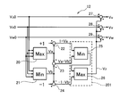
- FIG. 1 is a block diagram showing a circuit configuration of a power converter (inverter) 10 according to the first embodiment of the present invention.
- the inverter 10 of the present invention includes an inverter main circuit (inverter circuit) 15 and a control circuit 17 that controls the inverter main circuit 15.
- the control circuit 17 includes a basic voltage command generator 11, a voltage command corrector 12, a PWM pulse generator 13, and a gate driver 14. Further, the gate driver 14 includes a plurality of buffer circuits 16.
- a basic voltage command generator 11 receives a modulation factor M and a phase angle ⁇ , and has three-phase sinusoidal basic voltage commands Vu0, Vv0, Vw0 (first, second, and third basic sine waves). ) In accordance with the modulation factor M and the phase angle ⁇ . Details of the modulation factor M, the phase angle ⁇ , and the basic voltage command generator 11 will be described later.
- the voltage command corrector 12 adds the zero-phase signal Vz generated in the voltage command corrector 12 to the basic voltage commands Vu0, Vv0, Vw0, so that the voltage commands Vu, Vv, Vw (first, second, 3rd voltage command) is generated. Details of the voltage command corrector 12 will be described later.
- the PWM pulse generator 13 generates PWM pulse logic signals Pu1 to Pu4, Pv1 to Pv4, Pw1 to Pw4 based on the input voltage commands Vu, Vv, and Vw, and supplies them to the gate driver 14. Details of the PWM pulse generator 13 will be described later.
- the gate driver 14 is composed of a plurality of buffer circuits 16, by which the PWM pulse logic signals (Pu 1 to Pu 4, Pv 1 to Pv 4, Pw 1 to Pw 4) are transferred to the gate drive differential voltage electrical signal ( (Gu1 / Eu1 to Gu4 / Eu4, Gv1 / Ev1 to Gv4 / Ev4, Gw1 / Ew1 to Gw4 / Ew4) and supplied to the inverter main circuit 15. Details of the gate driver 14 and the buffer circuit 16 will be described later.
- the inverter main circuit 15 is a three-level inverter main circuit, and three-stage voltages (Ed, 0, ⁇ Ed) are applied to the output terminals U, V, and W of the inverter main circuit 15 by PWM control using a signal from the PWM pulse generator 13. ) PWM voltage waveform is generated. Details of the inverter main circuit 15 will be described later.
- the basic voltage command generator 11, the voltage command corrector 12, the PWM pulse generator 13, and the gate driver 14 constitute a control circuit 17 for PWM control of the inverter main circuit 15.
- Each circuit of the control circuit 17, or the basic voltage command generator 11, the voltage command corrector 12, the PWM pulse generator 13, and the gate driver 14, which are constituent elements thereof, is constituted by an electronic circuit or a microprocessor. It is manufactured by a software program as a control IC medium.
- the power converter (inverter) 10 using the PWM control method of the two-phase modulation method in which the amplitude of the zero-phase voltage and the zero-phase current is small compared to the prior art is embodied.
- the basic voltage command generator 11 has sinusoidal basic voltage commands Vu0, Vv0, Vw0 (first, second, third) defined according to the modulation factor M and the phase angle ⁇ , as shown in the following equation (1).
- Basic sine wave is generated and output.
- Vu0 M ⁇ sin ( ⁇ )
- Vv0 M ⁇ sin ( ⁇ 120 °)
- Vw0 M ⁇ sin ( ⁇ 240 °)
- the modulation factor M can be arbitrarily changed by a value of 0 to 2 / ⁇ 3.
- the phase angle ⁇ is given with a function that increases in proportion to the time t.
- FIG. 2 is a block diagram showing a circuit configuration of the voltage command corrector 12 provided in the power converter (inverter) 10 according to the first embodiment of the present invention.
- the voltage command corrector 12 includes maximum value selectors (Max) 20 and 26, minimum value selectors (Min) 21 and 25, adders 23, 27, 28 and 29, a subtractor 22, 24.
- the median value selector 201 includes the minimum value selector 25 and the maximum value selector 26.
- the maximum value selector 20 and the minimum value selector 21 receive basic voltage commands Vu0, Vv0, and Vw0.
- the maximum value selector 20 outputs the maximum value Va of the basic voltage commands Vu0, Vv0, Vw0 that change with time.
- the minimum value selector 21 outputs the minimum value Vb of the basic voltage commands Vu0, Vv0, Vw0.
- the subtractor 22 subtracts the maximum value Va from +1 to generate a signal (1-Va).
- the adder 23 adds the maximum value Va and the minimum value Vb to generate a signal (Va + Vb).
- the subtractor 24 subtracts the minimum value Vb from ⁇ 1 to generate a signal of ( ⁇ 1 ⁇ Vb).
- the minimum value selector 25 selects and outputs the smaller one of (1 ⁇ Va) and (Va + Vb).
- the maximum value selector 26 selects and outputs the larger value of the output signal of the minimum value selector 25 and ( ⁇ 1 ⁇ Vb).
- the signal of the maximum value selector 26 is equally applied to each of the sine wave basic voltage commands Vu0, Vv0, and Vw0 constituting the three phases, as will be described below, so that the sine wave basics constituting the three phases are applied. This corresponds to the zero phase component of the voltage commands Vu0, Vv0, Vw0. Therefore, the output signal of the maximum value selector 26 is referred to as a zero phase signal Vz.
- the adders 27, 28, and 29 add the zero-phase signal Vz to the basic voltage commands Vu0, Vv0, and Vw0 (first, second, and third basic sine waves) and respectively add the voltage commands Vu, Vv, and Vw. Output. That is, the voltage commands Vu, Vv, and Vw are shifted from the sinusoidal basic voltage commands Vu0, Vv0, and Vw0 constituting the three phases by the zero-phase signal Vz.
- the voltage commands Vu, Vv, and Vw are different from the sine waveform because they are shifted by the zero-phase signal Vz, but the line voltages (Vu ⁇ Vv), ( Vv ⁇ Vw) and (Vw ⁇ Vu) constitute a three-phase sine wave by canceling the zero-phase signal Vz. Therefore, if the line voltage is used, a three-phase load such as a motor can be driven without any trouble.
- the horizontal axis is the phase angle ⁇ (deg.), And the vertical axis is the value of each signal. However, the vertical axis is normalized by the maximum value of the basic voltage commands Vu0, Vv0, Vw0.
- the modulation factor M is 0.9
- the thick solid line is the zero phase signal (zero phase voltage command) Vz
- the thin broken lines are (1-Va), (Va + Vb), ( ⁇ 1 ⁇ Vb).
- FIG. 3A shows that the zero-phase signal Vz is selected from the median values of (1 ⁇ Va), (Va + Vb), and ( ⁇ 1 ⁇ Vb).
- the modulation factor M is 0.5
- the thick solid line is the zero-phase signal (zero-phase voltage command) Vz
- the thin broken lines are (1-Va) and (-1-Vb).
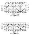
- FIG. 4 is a diagram illustrating waveforms of voltage commands Vu, Vv, and Vw generated by the voltage command corrector 12 included in the power conversion device according to the first embodiment of the present invention.
- (B) is when the modulation factor M is 0.5.
- the horizontal axis is the phase angle ⁇ (deg.), And the vertical axis is the value of each signal. However, the vertical axis is normalized by the maximum value of the voltage commands Vu, Vv, Vw.
- a thick solid line is Vu
- a thin solid line is Vv
- a thin broken line is Vw.
- the condition of the modulation rate at which the voltage commands Vu, Vv, and Vw are fixed at three voltage command values is 2/3 ⁇ M ⁇ 2 / ⁇ 3, and 0 ⁇ M ⁇ 2/3.
- the voltage command value is fixed only at a value of zero.
- the parameter ⁇ is a function ⁇ (M) determined depending on the modulation factor M, and is given by the following equation (2).
- ⁇ 30 °
- ⁇ is defined by the frequency method.
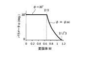
- FIG. 5 is a graph showing the relationship between the modulation factor M and the parameter ⁇ in the voltage command corrector provided in the power converter according to the first embodiment of the present invention.
- the horizontal axis of FIG. 5 is the modulation factor M
- the vertical axis is the parameter ⁇ (deg.).
- ⁇ is constant at 30 ° ( ⁇ / 6 radians) when M is smaller than 2/3
- ⁇ is M when M is larger than 2/3.
- FIG. 6 shows voltage commands Vu, Vv, Vw in the voltage command corrector provided in the power converter according to the first embodiment of the present invention, and voltage command values ⁇ 1, 0, +1 to which they are fixed. It is a figure showing the relationship which put together the length of the phase angle range used as the conditions where a voltage command is fixed, and the phase angle range. Note that the phase angle range is expressed in the power method (deg.). In FIG.
- the range of the phase angle ⁇ in which the voltage command value is fixed to +1 is 60 ° + ⁇ ⁇ ⁇ 120 ° ⁇ , and the phase angle ⁇ in which the voltage command value is fixed to 0.
- the range is 0 ⁇ ⁇ ⁇ , 180 ° ⁇ ⁇ ⁇ 180 ° + ⁇ , 360 ° ⁇ ⁇ 360 °, and the range of the phase angle ⁇ in which the voltage command value is fixed to ⁇ 1 is 240 ° + ⁇ ⁇ ⁇ 300 ° - ⁇ .
- the lengths of the phase angle ranges in which the voltage command value is fixed to ⁇ 1, 0, ⁇ 1 are 60 ° ⁇ 2 ⁇ , 4 ⁇ , and 60 ° ⁇ 2 ⁇ , respectively.
- (60 ° -2 ⁇ ) + (4 ⁇ ) + (60 ° -2 ⁇ ) 120 °
- the total length of is 120 °.
- FIG. 7 is a block diagram showing a circuit configuration of the PWM pulse generator 13 provided in the power conversion device according to the first embodiment of the present invention.
- the PWM pulse generator 13 includes a triangular wave generator 31, a subtractor 32, comparators 33u, 33v, 33w, 34u, 34v, 34w, logic inversion circuits 35u, 35v, 35w, 36u, 36v, 36w, and ON delay.
- the circuit 37 is configured.
- the triangular wave generator 31 generates the carrier triangular wave signal Vcar1 (first carrier triangular wave signal) shown in FIG. 8, and the subtracter subtracts 1 from the value of Vcar1 to thereby generate the carrier triangular wave signal Vcar2 (second carrier triangular wave signal). ).
- the detailed waveforms of the carrier triangular wave signals Vcar1 and Vcar2 will be described later with reference to FIG.
- the comparator 33u compares the voltage command Vu with a triangular wave (carrier triangular wave signal) Vcar1. Further, the comparator 34u compares the voltage command Vu with the triangular wave Vcar2.
- the logic inverting circuit 35u receives the signal from the comparator 33u and outputs the inverted signal.
- the logic inversion circuit 36u receives the signal from the comparator 34u and outputs the inverted signal.
- four types of PWM pulse logic signals Pu1 to Pu4 are generated by combining with the comparators 33u and 34u and the logic inverting circuits 35u and 36u.
- the PWM pulse logic signals Pu1 to Pu4 are output via the ON delay circuit 37. The function of the ON delay circuit 37 will be described later.
- the comparators 33u and 34u usually generate a pulse in any one of Pu1 to Pu4 every period 1 / fc.
- the amplitudes of Vcar1 and Vcar2 of the triangular wave (carrier triangular wave signal) are slightly smaller than 1 (predetermined value)
- pulses are generated in Pu1 to Pu4 only when the voltage command Vu is +1, 0, -1. do not do.
- the predetermined value is a condition that only when the voltage command Vu is +1, 0, ⁇ 1, no pulse is generated in Pu1 to Pu4, and the apex of the triangular wave is close to +1 (or 0, or ⁇ 1).
- a value selected within a range that does not malfunction due to noise or the like is a value selected within a range that does not malfunction due to noise or the like.
- the configurations of the comparators 33v and 34v and the logic inverting circuits 35v and 36v are basically the same as the configurations of the comparators 33u and 34u and the logic inverting circuits 35u and 36u described above, and thus redundant description is omitted. Therefore, a circuit combining the comparators 33v and 34v and the logic inverting circuits 35v and 36v generates the PWM pulse logic signals Pv1 to Pv4 based on the voltage command Vv. Similarly, a circuit combining comparators 33w and 34w and logic inversion circuits 35w and 36w generates PWM pulse logic signals Pw1 to Pw4 based on voltage command Vw.
- the ON delay circuit 37 is a delay circuit for slightly delaying the time when the PWM pulse logic signal becomes H level. However, when the PWM pulse logic signal becomes L level, it is quickly made L level. When the ON delay circuit 37 is at the H level and the L level, a delay time is provided, thereby providing a dead time for the switching operation of the transistor to which the PWM pulse logic signal is supplied, and variations in signal delay, etc. Prevents accidental short circuit.
- FIG. 8 is a diagram showing waveforms of carrier triangular wave signals Vcar1 and Vcar2 in the PWM pulse generator provided in the power conversion device according to the first embodiment of the present invention.
- the horizontal axis is the time transition, and the vertical axis is the signal voltage, normalized.
- carrier triangular wave signals Vcar1 and Vcar2 are triangular waves having a frequency of PWM carrier frequency fc and a voltage amplitude slightly smaller than 1 (predetermined value).
- the carrier triangular wave signal Vcar1 sweeps between 0 and +1
- the carrier triangular wave signal Vcar2 sweeps between ⁇ 1 and 0.
- the white circle portion indicates that the solid line of the triangular wave does not reach the broken line slightly. That is, as described above, Vcar1 is a triangular wave that can take a value between 0 and +1 and Vcar2 can take a value between -1 and 0, but does not take a value of +1, 0, or -1.
- the gate driver 14 includes 12 buffer circuits 16 that convert PWM pulse logic signals Pu1 to Pu4, Pv1 to Pv4, and Pw1 to Pw4 into differential voltage electrical signals that are isolated from each other. ing.
- the PWM pulse logic signals (Pu1 to Pu4, Pv1 to Pv4, Pw1 to Pw4) are converted into gate drive differential voltage electrical signals (Gu1 / Eu1 to Gu4 / Eu4, Gv1 / Ev1 to Gv4 / Ev4, Gw1 / Ew1 to Gw4 / Ew4). ) And supplied to the inverter main circuit 15.
- the Pu1 signal is generated as a differential voltage electric signal from the buffer circuit 16 via the buffer circuit 16, and a differential voltage is generated between Gu1 and Eu1 and output as two signals.
- the buffer circuit 16 can isolate output signals from each other by adopting an isolator such as a photocoupler, and has a high gate drive capability by employing a low impedance output circuit such as a push-pull circuit. be able to.
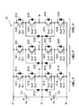
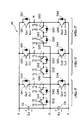
- FIG. 9 is a diagram showing a circuit configuration of the inverter main circuit 15 provided in the power conversion device according to the first embodiment of the present invention.
- the inverter main circuit 15 includes a positive DC power supply P (node P), a negative DC power supply N (node N), and a neutral DC power supply O (node O).
- the node O at the neutral point may be grounded.
- a capacitor C1 is connected between the positive DC power supply P and the neutral DC power supply O, and the voltage of Ed is applied.
- a capacitor C2 is connected between the neutral DC power supply O and the negative DC power supply N, and the voltage of Ed is applied.
- a U-phase leg, a V-phase leg, and a W-phase leg configured by including a transistor and a diode between the positive DC power source P and the negative DC power source N are configured in a parallel configuration corresponding to three phases. Has been.
- the U-phase leg includes transistors Q11 to Q14 and diodes D11 to D16.
- Transistors Q11 to Q14 made of IGBT (Insulated Gate Bipolar Transistor) are connected in series, the collector of the transistor Q11 is connected to a positive DC power supply P, and the emitter of the transistor Q14 is connected to a negative DC power supply N.
- the emitter of the transistor Q12 and the collector of the transistor Q13 are connected to each other and to the output terminal U as a U-phase leg.
- the diodes D11 to D14 are connected in antiparallel to the transistors Q11 to Q14, respectively.
- the anode of the diode D15 is connected to the DC power source O at the neutral point, and the cathode is connected to the connection point between the emitter of the transistor Q11 and the collector of the transistor Q12.
- the cathode of the diode D16 is connected to a neutral direct current power source O, and the anode is connected to the connection point between the emitter of the transistor Q13 and the collector of the transistor Q14.
- Gu1 and Eu1 are applied as a differential voltage electrical signal (Gu1 / Eu1) from the gate driver 14 to the gate and emitter of the transistor Q11 formed of an IGBT, respectively. That is, a signal is applied as a voltage difference between the gate and the emitter.
- Gu2 and Eu2 are applied to the gate and emitter of the transistor Q12 as the differential voltage electrical signal (Gu2 / Eu2) from the gate driver 14, respectively.
- Gu3 and Eu3 are applied to the gate and emitter of the transistor Q13 as differential voltage electrical signals (Gu3 / Eu3) from the gate driver 14, respectively.
- Gu4 and Eu4 are applied to the gate and emitter of the transistor Q14 as differential voltage electrical signals (Gu4 / Eu4) from the gate driver 14, respectively. From the above, the U-phase leg is configured.
- the V phase includes transistors Q21 to Q24 and diodes D21 to D26, and is configured to correspond to the U phase transistors Q11 to Q14 and the diodes D11 to D16, respectively.
- the transistors Q21 to Q24 have the same relationship as that of the U-phase transistors Q11 to Q14 in the differential voltage electrical signals (Gv1 / Ev1), (Gv2 / Ev2), (Gv3 / Ev3), and (Gv4 / Ev4), respectively. It is connected.
- the W phase includes transistors Q31 to Q34 and diodes D31 to D36, and is configured to correspond to the U phase transistors Q11 to Q14 and the diodes D11 to D16, respectively.
- the transistors Q31 to Q34 have the same relationship between the differential voltage electrical signals (Gw1 / Ew1), (Gw2 / Ew2), (Gw3 / Ew3), and (Gw4 / Ew4) as the U-phase transistors Q11 to Q14, respectively. It is connected.
- the DC positive voltage + Ed is applied from the node P and the DC negative voltage -Ed is applied from the node N to each of the U-phase, V-phase, and W-phase legs. Further, a zero voltage (0 potential) is applied from the node O. As described above, the capacitors C1 and C2 are connected between the node PO and the node ON to hold the DC voltage Ed between the nodes.
- each of the U-phase, V-phase, and W-phase legs converts the PWM pulse logic signals Pu1 to Pu4, Pv1 to Pv4, and Pw1 to Pw4 of the PWM pulse generator into a differential voltage electrical signal (Gu1 / Eu1 to (Gu4 / Eu4, Gv1 / Ev1 to Gv4 / Ev4, Gw1 / Ew1 to Gw4 / Ew4) are controlled by the signal so that the inverter main circuit 15 converts the DC voltage (power) into the three-phase AC voltage (power). Fulfills the function of converting to
- the transistors have a silicon IGBT or a silicon MOSFET (Metal-Oxide-) as a switch device (switching device) for ease of turn-on / turn-off control.
- Semiconductor Field-Effect Transistor is preferably used.
- a silicon PiN diode or a silicon Schottky barrier diode as the diodes (D11 to D16, D21 to D26, D31 to D36).
- a wide gap device wide gap power device including a semiconductor having a larger band gap than silicon instead of the silicon device.
- a SiC (Silicon Carbide) device can be applied.
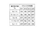
- FIG. 10 is a diagram showing the relationship between the transistors Q11 to Q14 constituting the U-phase leg and the voltage command Vu in the inverter main circuit provided in the power conversion device according to the first embodiment of the present invention.
- the transistors Q11 to Q14 constituting the U-phase leg perform a switching operation according to the voltage command Vu.
- “ON” represents an ON state
- “OFF” represents an OFF state
- “SW” represents a switching state (a repeated state of ON and OFF).
- the transistor Q11 and the transistor Q13 perform a switching operation.
- the transistor Q12 and the transistor Q14 perform a switching operation.
- the transistors Q11 to Q14 are fixed to either ON or OFF, and no switching operation is performed. Therefore, when the voltage command Vu is +1, 0, ⁇ 1, no switching loss occurs in the U-phase leg.
- the voltage commands Vv, Vw are +1, 0, ⁇ 1, respectively, no switching loss occurs in the V-phase leg and the W-phase leg.
- the power conversion device (inverter) 10 reduces switching loss (power consumption), loss due to zero-phase current, and high-frequency noise.
- FIG. 11 is a diagram illustrating a voltage waveform output to the output terminal U of the U-phase leg in the inverter main circuit provided in the power conversion device according to the first embodiment of the present invention.
- (B) is a voltage waveform when the modulation factor M is 0.5.
- the horizontal axis represents the phase angle ⁇ (deg.)
- the vertical axis represents the output voltage.
- the carrier frequency fc used for PWM control is set to 100 times the fundamental frequency f1 constituting a three-phase AC sine wave.
- phase angle is other than the above, a PWM waveform having an amplitude Ed is output to the output terminal U.
- the above applies not only when the modulation factor M is 0.9, but also when the modulation factor 2/3 ⁇ M ⁇ 2 / ⁇ 3.
- ⁇ is the parameter ⁇ described above.
- FIGS. 11 (a) and 11 (b) show that the switching operation of the U-phase leg stops in the range of the phase angle length of 120 °, that is, a period of 1/3 of the whole. Further, for the same reason, the switching operation of the U-phase leg is stopped in the 1/3 overall period for the V-phase leg and the W-phase leg.
- the output of the inverter main circuit 15 is also the output of the power converter device (inverter) 10 of this invention. Therefore, it is also a characteristic of the power conversion device (inverter) 10.
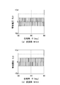
- FIG. 12 is a diagram illustrating a frequency spectrum of a voltage waveform output to the output terminal U of the inverter main circuit 15 provided in the power conversion device according to the first embodiment of the present invention.
- (B) is a frequency spectrum when the modulation factor M is 0.5.
- the horizontal axis represents the harmonic order n, and the vertical axis represents the amplitude value Vn / Ed of the nth-order frequency component Vn.
- the carrier frequency fc is set to 99 times the basic frequency f1.
- V1 is a component of the fundamental frequency f1
- its amplitude value V1 / Ed is 0.90 in FIG. 12A, which is the same value as the modulation factor (0.9).
- FIG. 12B it is 0.50, which is the same value as the modulation rate (0.5).
- V99 is a component of the carrier frequency fc
- its amplitude value V99 / Ed is 0.32 in FIG. 12A and 0.30 in FIG.
- the third-order component V3 is 0.14 in FIG. 12A and 0.21 in FIG.
- FIG. 13 shows the frequency spectrum of the voltage waveform of the output of the three-level inverter to which the control characteristic two-phase modulation method shown in FIG. 19 is applied as a comparative example. And it compares with the frequency spectrum of the voltage waveform of the output of the inverter 10 of this invention mentioned above in FIG.
- the inverter 10 of the present invention is also a three-level inverter to which the two-phase modulation method is applied.
- FIG. 13 is a diagram illustrating a frequency spectrum of a voltage waveform output from a three-level inverter to which a two-phase modulation method of a comparative example described later is applied.
- FIG. ) Is a frequency spectrum when the modulation factor M is 0.5.
- the horizontal axis represents the harmonic order n, and the vertical axis represents the amplitude value Vn / Ed of the nth-order frequency component Vn.
- the carrier frequency fc is set to 99 times the basic frequency f1.
- V1 is a component of the fundamental frequency f1
- its amplitude value V1 / Ed is 0.90 in FIG. 13A, which is the same value as the modulation factor (0.9). .
- V99 is a component of the carrier frequency fc, and its amplitude value V99 / Ed is 0.30 in FIG. 13A and 0.31 in FIG.
- the third harmonic component V3 is 0.16 in FIG. 13A and 0.66 in FIG.
- V9 of the 9th harmonic component and V15 of the 15th harmonic component appear at conspicuous levels.
- FIG. 12 and FIG. 13 which are inverters of the present invention and the comparative example. Comparing FIG. 12 and FIG. 13, most amplitude values of the frequency component Vn of the voltage waveform output to the output terminal U of the first embodiment of the present invention are smaller than that of the two-phase modulation method of the comparative example. ing. In particular, this tendency becomes stronger as the modulation factor M is smaller.
- the amplitude values of higher harmonic components V9, V15, etc. are more significant than the third harmonic component V3.
- these are almost eliminated.
- the inverter using the PWM control method of the present invention can suppress the harmonic component contained in the output voltage waveform to be smaller than that of the inverter using the two-phase modulation method of the comparative example. This tendency is particularly remarkable when the modulation rate is small.
- FIG. 14 is a diagram illustrating a waveform of the zero-phase voltage Ez3 included in the output voltage of the power conversion device (inverter) 10 or the inverter main circuit 15 according to the first embodiment of the present invention.
- the modulation factor M is 0.9
- (b) is a waveform when the modulation factor M is 0.5.
- the vertical axis represents the zero-phase voltage Ez3
- the horizontal axis represents the phase angle ⁇
- the phase angle ⁇ 0 ° to 360 °, and the range of 30 ° to 90 °.
- 14A and 14B show that the amplitude of the zero-phase voltage Ez3 generated by the inverter 10 is within ⁇ 1/3 of the DC voltage Ed. Note that the characteristics of FIG. 14 will be further described while comparing the characteristics of the comparative example shown in FIG.
- FIG. 15 is a diagram showing a waveform of the zero-phase voltage Ez2 included in the output voltage of the three-level inverter using the two-phase modulation method of the comparative example described later.
- FIG. 15A shows a modulation factor M of 0.9.
- (B) is a waveform when the modulation factor M is 0.5.
- the vertical axis represents the zero-phase voltage Ez2
- the horizontal axis represents the phase angle ⁇
- the phase angle ⁇ 0 ° to 360 °
- the range of 30 ° to 90 ° is included. Extracted and shown.
- the inverter of the first embodiment of the present invention corresponds to the waveform of the voltage command value of FIG. 4, and the waveform of FIG. 15 of the inverter of the comparative example is the voltage command of FIG. Corresponds to the value waveform. That is, selecting the waveform of the voltage command value of the inverter of the PWM control method of the present invention as shown in FIG. 4 reduces the zero-phase current and brings about the above effect.
- FIG. 16 is a diagram showing a measurement circuit for the zero-phase voltage Ez3 of the power converter (inverter) 10 according to the first embodiment of the present invention and the zero-phase voltage Ez2 of the comparative example.
- the same resistance as the reactor Lac having the same reactor value is applied to the output terminals U, V, and W of the inverter (10) with the node O of the inverter 10 of the first embodiment of the present invention or the inverter of the comparative example as the ground potential.
- a series circuit of value resistors Rac is connected to each other, and a ground voltage of a node at a portion where one ends of the resistors Rac are connected to each other is observed. With this measurement, the zero-phase voltage Ez (Ez3, Ez2) can be observed.
- FIG. 17 is a diagram showing a circuit configuration of the inverter main circuit 45 provided in the power conversion device according to the second embodiment of the present invention.
- the inverter main circuit 45 includes a positive DC power supply P (node P), a negative DC power supply N (node N), and a neutral DC power supply O (node O).
- a capacitor C3 is connected between the positive DC power supply P and the neutral DC power supply O, and the voltage of Ed is applied.
- a capacitor C4 is connected between the neutral DC power supply O and the negative DC power supply N, and the voltage of Ed is applied.
- a U-phase leg, a V-phase leg, and a W-phase leg configured by including a transistor and a diode between the positive DC power source P and the negative DC power source N are configured in a parallel configuration corresponding to three phases. Has been.
- the U-phase leg includes transistors Q41 to Q44 and diodes D41 to D44.
- An IGBT transistor Q41 and a transistor Q44 are connected in series, a collector of the transistor Q41 is connected to a positive DC power supply P (node P), and an emitter of the transistor Q44 is connected to a negative DC power supply N (node N). Yes.
- the emitter of the transistor Q41 and the collector of the transistor Q44 are connected to each other and to the output terminal U as a U-phase leg.
- the transistor Q42 and the transistor Q43 are connected in series via each other's collector, the emitter of the transistor Q42 is connected to the node O, and the emitter of the transistor Q43 is connected to the output terminal U.
- the diodes D41 to D44 are connected in antiparallel to the transistors Q41 to Q44, respectively.
- Gu1 and Eu1 are applied to the gate and emitter of the transistor Q41 formed of IGBT as a differential voltage electrical signal (Gu1 / Eu1) from the gate driver 14, respectively.
- Gu2 and Eu2 are applied to the gate and emitter of the transistor Q42 as differential voltage electrical signals (Gu2 / Eu2) from the gate driver 14, respectively.
- Gu3 and Eu3 are applied to the gate and emitter of the transistor Q43 as differential voltage electrical signals (Gu3 / Eu3) from the gate driver 14, respectively.
- Gu4 and Eu4 are applied to the gate and emitter of the transistor Q44 as differential voltage electrical signals (Gu4 / Eu4) from the gate driver 14, respectively. From the above, the U-phase leg is configured.
- connection configuration of the transistor Q42 and the transistor Q43 is different from the configuration of the connection of the transistor Q12 and the transistor Q13 of the inverter main circuit 15 (FIG. 9) of the first embodiment, but the output terminal as a U-phase leg. From U, a substantially similar output waveform is output.
- the V phase includes transistors Q51 to Q54 and diodes D51 to D54, and is configured to correspond to the U phase transistors Q41 to Q44 and the diodes D41 to D44, respectively.
- the differential voltage electrical signals Gv1 / Ev1), (Gv2 / Ev2), (Gv3 / Ev3), and (Gv4 / Ev4) are respectively related to the transistors Q51 to Q54 in the same relationship as the U-phase transistors Q41 to Q44. Connected with.
- the W phase includes transistors Q61 to Q64 and diodes D61 to D64, and is configured to correspond to the U phase transistors Q41 to Q44 and the diodes D41 to D44, respectively.
- the differential voltage electrical signals (Gw1 / Ew1), (Gw2 / Ew2), (Gw3 / Ew3), and (Gw4 / Ew4) are respectively connected to the transistors Q61 to Q64 in the same relationship as the U-phase transistors Q11 to Q14. Connected with.
- the DC positive voltage + Ed is applied from the node P and the DC negative voltage -Ed is applied from the node N to the U-phase, V-phase, and W-phase legs, and the zero voltage (0 potential) is applied from the node O. ) Is given.
- the capacitors C3 and C4 are connected between the node PO and the node ON to hold the DC voltage Ed between the nodes.
- each of the U-phase, V-phase, and W-phase legs converts the PWM pulse logic signals Pu1 to Pu4, Pv1 to Pv4, and Pw1 to Pw4 of the PWM pulse generator into a differential voltage electrical signal (Gu1 / Eu1 to (Gu4 / Eu4, Gv1 / Ev1 to Gv4 / Ev4, Gw1 / Ew1 to Gw4 / Ew4) are controlled by the signal so that the inverter main circuit 45 converts the DC voltage (power) into the three-phase AC voltage (power). Fulfills the function of converting to
- the number of diode elements can be reduced by six compared to the circuit of FIG.
- the number of series-connected transistors and diodes between the output terminals U, V, and W, and the nodes P and N is reduced from 2 to 1, these elements are required to have double withstand voltage.
- a wide gap device wide gap power device
- a semiconductor element having a larger band gap than silicon instead of the silicon device.
- a SiC device can be applied.
- a silicon IGBT or a silicon MOSFET for the transistor used in the circuit of FIG. 17 because of easy control of turn-on / turn-off.
- the diode a silicon PiN diode or a silicon Schottky barrier diode is used.
- Comparative example As a comparative example, an example in which the voltage command of the two-phase modulation method when the voltage command value is not fixed to 0 is applied to a three-level inverter is shown below.
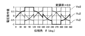
- FIG. 18 is a diagram illustrating an example of the voltage command of the two-phase modulation method of the comparative example (when the voltage command value is not fixed to 0).
- the vertical axis represents the (normalized) voltage command value, and the horizontal axis represents the phase angle.
- the voltage commands Vu2, Vv2, and Vw2 are generated by adding a zero-phase signal to the basic sine wave signal.
- the waveforms (Vu2, Vv2, Vw2) in FIG. 18 a phase angle range in which the voltage command value is fixed at +1 and ⁇ 1 is formed.
- the voltage command Vu2 is fixed to +1 at a phase angle of 60 ° to 120 °, and is fixed to ⁇ 1 at a phase angle of 240 ° to 300 °. Note that the range in which the voltage command value is fixed at 0 as shown in FIG. 4 of the present invention does not exist in FIG. 18 of the comparative example.
- the PWM voltage waveform (only one phase is shown) shown in FIG. 19 can be output.
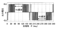
- FIG. 19 is a diagram illustrating a PWM voltage waveform (U phase) obtained by applying the voltage command of the two-phase modulation method of the comparative example to the three-level inverter.
- the vertical axis represents the output voltage
- the horizontal axis represents the phase angle.
- the PWM voltage waveform shown in FIG. 19 is obtained by comparing the voltage command value shown in FIG. 18 with two carrier triangular waves having amplitudes of 0 to +1 and ⁇ 1 to 0 and a PWM signal obtained by a comparator. It is obtained by switching the transistor.
- FIG. 19 is a diagram illustrating a PWM voltage waveform (U phase) obtained by applying the voltage command of the two-phase modulation method of the comparative example to the three-level inverter.
- the vertical axis represents the output voltage
- the horizontal axis represents the phase angle.
- the PWM voltage waveform shown in FIG. 19 is obtained by comparing the voltage command value shown in FIG. 18 with two carrier triangular waves having ampli
- the output voltage waveform (PWM voltage waveform) is fixed to + Ed at a phase angle of 60 ° to 120 °, and is fixed to ⁇ Ed at a phase angle of 240 ° to 300 °. Therefore, the switching operation of the three-level inverter can be stopped at 120 ° out of the total phase angle 360 °. Therefore, in each switch element constituting the inverter, the number of times of switching can be reduced to 2/3, and the switching loss can be reduced.
- Patent Document 1 and Patent Document 2 describe a two-phase modulation method and a PWM control method for stopping switching of a transistor for a certain period as in the case of two-phase modulation. Note that the two-phase modulation method does not distort the sinusoidal shape of the line voltage even if the modulation rate is increased to 2 / ⁇ 3, which is larger than 1, so that the voltage utilization rate can be increased. I have. However, the two-phase modulation method of the comparative example shown in FIGS. 18 and 19 is a method of fixing the voltage command value to +1 or ⁇ 1 but not fixing it to 0.
- the voltage command value is fixed to 0 within a predetermined phase angle range.
- the present invention uses a zero-phase voltage command that reduces the generation of harmonics, so that there is little zero-phase current, and there is an effect of reducing power consumption and noise due to harmonics and zero-phase current. This is particularly noticeable when the modulation rate is small.
- Control circuit 17 ⁇ Control circuit 17
- the control circuit 17 that controls the inverter main circuit 15 has been described as being configured with the basic voltage command generator 11, the voltage command corrector 12, the PWM pulse generator 13, and the gate driver 14. It is not limited.
- the gate driver 14 may be included in the PWM pulse generator 13.
- the basic voltage command generator 11 and the voltage command corrector 12 may be integrated.
- the basic voltage command generator 11, the voltage command corrector 12, and the PWM pulse generator 13 may be configured by individual hardware circuits, MPU (Micro-Processing Unit), A configuration may be adopted in which control is performed collectively by a software program using a control IC such as a CPU (Central Processing Unit) as a medium.
- MPU Micro-Processing Unit
- the transistor is described as an IGBT, and the possibility of using a MOSFET instead has been described.
- the transistor basically needs to be a switching element, it is limited to an IGBT or a MOSFET.
- BJT Bipolar junction transistor
- BiCMOS Bipolar Complementary Metal Oxide Semiconductor
- SiC SiC was mentioned as a wide gap device, it is not limited to this.
- a semiconductor device such as GaN (gallium nitride) or Ga 2 O 3 (gallium oxide) may be used.
- diode 9 and 17 it has been described that the diodes (D11 to D14, D21 to D24, D31 to D34, D41 to D44, D51 to D54, D61 to D64) are connected in reverse parallel to the transistor (IGBT).
- IGBT transistor
- a parasitic diode incorporated in a transistor (IGBT, MOSFET) may be used without being added as an element.
Landscapes
- Engineering & Computer Science (AREA)
- Power Engineering (AREA)
- Inverter Devices (AREA)
Abstract
The present invention is provided with: an inverter circuit in which a plurality of switching devices are configured to use a direct-current voltage (+Ed, -Ed) as a power source, and to output the PWM voltage waveform at three levels (+Ed, 0, and -Ed); and a control circuit for turning the plurality of switching devices on and off, and generating the PWM voltage waveform on the basis of the output of the inverter circuit. The control circuit: controls the amplitude of the fundamental frequency component of the PWM voltage waveform in proportion to a prescribed modulation factor (M); during one cycle of the fundamental frequency component, fixes the output voltage of the inverter circuit at +Ed, 0, or -Ed relative to a specified phase angle range for the fundamental frequency component; fixes the output voltage of the inverter circuit at all of the voltages +Ed, 0, and -Ed in the specified phase angle range when the modulation (M) is 2/3 or greater; and fixes the output voltage of the inverter circuit at a voltage of 0 in the specified phase angle range when the modulation (M) is less than 2/3.
Description
本発明は、直流電圧を三相交流電圧に変換する3レベルインバータのPWM(Pulse Width Modulation)制御方法(制御方式)とそれを用いた電力変換装置に関するものである。
The present invention relates to a PWM (Pulse Width Modulation) control method (control method) of a three-level inverter that converts a DC voltage into a three-phase AC voltage, and a power converter using the same.
直流電圧(電流)を三相の交流電圧(電流)に変換するPWM制御インバータ装置(PWM制御方法を用いた電力変換装置)は、モータ制御、無停電電源装置、パワーコンディショナ、周波数電力変換装置などに使用されている。PWM制御方法を代表する方法として、三角波比較方法(方式)(Sub-harmonic Method)が広く知られている。
三角波比較方法では、三角波のキャリア信号と、正弦波状の電圧指令とを比較し、電圧指令が高い場合には高い電圧ノードに接続したトランジスタをON(オン)させ、低い場合には低い電圧ノードに接続したトランジスタをONさせる。この制御により、三相の正弦波に相当する相電圧が得られる。
また、PWM制御インバータ装置としては、2レベルインバータと3レベルインバータがある。 PWM control inverter device (power converter using PWM control method) that converts DC voltage (current) into three-phase AC voltage (current) is motor control, uninterruptible power supply, power conditioner, frequency power converter It is used for such as. As a method representative of the PWM control method, a triangular wave comparison method (sub-harmonic method) is widely known.
In the triangular wave comparison method, a triangular wave carrier signal and a sinusoidal voltage command are compared. When the voltage command is high, the transistor connected to the high voltage node is turned on, and when the voltage command is low, the low voltage node is set. Turn on the connected transistor. By this control, a phase voltage corresponding to a three-phase sine wave is obtained.
As the PWM control inverter device, there are a two-level inverter and a three-level inverter.
代表的なインバータである2レベルインバータは、インバータ主回路に直流電圧+Ed,-Edを入力し、出力1相あたり2個のトランジスタで構成されたレグ回路によって、正(+Ed)、負(-Ed)の2段階のPWM電圧波形を出力する。
これに対して、3レベルインバータは、インバータ主回路に直流電圧+Ed,-Edと、コンデンサにより2分割して得られる0電位を入力し、出力1相あたり4個のトランジスタで構成されたレグ回路によって、正(+Ed)、負(-Ed)、および0の3段階のPWM電圧波形を出力できるインバータである。なお、3レベルインバータは、2レベルインバータと比較して、スイッチングによる出力電圧の変化率が1/2になるため、インバータ主回路を構成するスイッチ素子のスイッチング電圧を1/2にすることでスイッチング損失を減らすことができる。 A two-level inverter, which is a typical inverter, inputs a DC voltage + Ed, -Ed to an inverter main circuit, and is positive (+ Ed), negative (-Ed) by a leg circuit composed of two transistors per output phase. 2) PWM voltage waveform in two stages.
In contrast, a three-level inverter inputs a DC voltage + Ed, -Ed and a zero potential obtained by dividing into two by a capacitor to the inverter main circuit, and a leg circuit composed of four transistors per output phase. Thus, the inverter can output three-stage PWM voltage waveforms of positive (+ Ed), negative (−Ed), and 0. Since the change rate of the output voltage due to switching is halved in the 3-level inverter compared to the 2-level inverter, switching is performed by halving the switching voltage of the switch elements constituting the inverter main circuit. Loss can be reduced.
また、トランジスタのスイッチングを一定期間停止させ、インバータ主回路のスイッチング回数を減らすことでスイッチング損失を低減するPWM制御方法として二相変調方法(方式)がある。
二相変調方法は、三相のうちの一相のスイッチ素子(スイッチングデバイス)に与える電圧指令が三角波キャリアの最大値あるいは最小値になるように各相に零相成分の信号を加え、スイッチ素子を所定の間ONあるいはOFF(オフ)の状態に固定することである。この方法により基本波成分の線間電圧を変化させることなくトランジスタのスイッチング損失を低減できる。一般的には、出力周波数の位相角に対して60度毎に電圧モードを切り替え、各相が順番に常時ONあるいはOFFの状態になるように制御する。
また、二相変調方法は、変調率を1より大きい2/31/2まで高めても、線間電圧の正弦波形状に歪みを与えることが無いので、電圧利用率を大きくすることができる特徴も備えている。なお、「31/2」は、ルート3であるが、適宜、簡略化して「√3」と表記する。 There is a two-phase modulation method (method) as a PWM control method for reducing switching loss by stopping transistor switching for a certain period and reducing the number of times the inverter main circuit is switched.
In the two-phase modulation method, a zero-phase component signal is added to each phase so that the voltage command given to one phase switching element (switching device) of the three phases becomes the maximum value or the minimum value of the triangular wave carrier. Is fixed to an ON or OFF state for a predetermined period. By this method, the switching loss of the transistor can be reduced without changing the line voltage of the fundamental wave component. Generally, the voltage mode is switched every 60 degrees with respect to the phase angle of the output frequency, and control is performed so that each phase is always in an ON or OFF state in order.
Further, in the two-phase modulation method, even if the modulation rate is increased to 2/3 1/2 , which is larger than 1, the voltage utilization rate can be increased because the sinusoidal shape of the line voltage is not distorted. It also has features. Note that “3 1/2 ” is the route 3, but is simply simplified as “√3”.
前記の二相変調方法の詳細は、比較例として図18、図19を参照して後記する。
2レベルインバータに二相変調方法を適用した技術は、特許文献1に開示されている。
また、3レベルインバータに、前記二相変調方法と同様に、トランジスタのスイッチングを一定期間停止するPWM制御方法を適用した技術は、特許文献2に開示されている。 Details of the two-phase modulation method will be described later with reference to FIGS. 18 and 19 as comparative examples.
A technique in which a two-phase modulation method is applied to a two-level inverter is disclosed inPatent Document 1.
Further, as in the two-phase modulation method, a technique in which a PWM control method for stopping switching of a transistor for a certain period is applied to a three-level inverter is disclosed in Patent Document 2.
2レベルインバータに二相変調方法を適用した技術は、特許文献1に開示されている。
また、3レベルインバータに、前記二相変調方法と同様に、トランジスタのスイッチングを一定期間停止するPWM制御方法を適用した技術は、特許文献2に開示されている。 Details of the two-phase modulation method will be described later with reference to FIGS. 18 and 19 as comparative examples.
A technique in which a two-phase modulation method is applied to a two-level inverter is disclosed in
Further, as in the two-phase modulation method, a technique in which a PWM control method for stopping switching of a transistor for a certain period is applied to a three-level inverter is disclosed in Patent Document 2.
特許文献1、2に開示された二相変調方法を適用した技術においては、後記(図18)するように、二相変調方法の電圧指令に、位相角60°毎に不連続点が存在する。
そのため、電圧指令が不連続であるタイミングで、インバータの出力電圧が跳躍(短時間に急激に変化)し、対地コンデンサや、インバータ出力に接続された配線、負荷(モータ、あるいは変圧器など)に存在する対地間の寄生静電容量を通じて、零相電流が発生する。この零相電流は、対地コンデンサでの電力損失を生じさせる。また零相電流は、寄生静電容量を通した系統電源への流出によって、周辺機器への悪影響をもたらす可能性がある。
また、二相変調方法は、出力の相電圧に高調波を多く含むため、高調波ノイズの原因となる。また、この高調波は、対地コンデンサなどの電力損失の一層の増加をもたらす。
変調率が高い(2/√3に近い)場合には、前記の出力電圧の跳躍電圧幅や、高調波は小さいが、変調率が低い場合には、前記の出力電圧の跳躍電圧幅や、高調波が大きくなるため、零相電流および高調波が引き起こす悪影響が大きくなる。 In the technology to which the two-phase modulation method disclosed inPatent Documents 1 and 2 is applied, as will be described later (FIG. 18), there are discontinuities in the voltage command of the two-phase modulation method every phase angle of 60 °. .
Therefore, the output voltage of the inverter jumps at a timing when the voltage command is discontinuous (changes rapidly in a short time), and is connected to the ground capacitor, the wiring connected to the inverter output, and the load (motor, transformer, etc.) A zero-phase current is generated through the existing parasitic capacitance between the ground. This zero-phase current causes a power loss in the ground capacitor. In addition, the zero-phase current may adversely affect peripheral devices due to the outflow to the system power supply through the parasitic capacitance.
In addition, since the two-phase modulation method includes many harmonics in the output phase voltage, it causes harmonic noise. This harmonic also causes a further increase in power loss such as a ground capacitor.
When the modulation factor is high (close to 2 / √3), the output voltage jump voltage width and harmonics are small, but when the modulation factor is low, the output voltage jump voltage width, Since the harmonics become large, the adverse effects caused by the zero-phase current and the harmonics become large.
そのため、電圧指令が不連続であるタイミングで、インバータの出力電圧が跳躍(短時間に急激に変化)し、対地コンデンサや、インバータ出力に接続された配線、負荷(モータ、あるいは変圧器など)に存在する対地間の寄生静電容量を通じて、零相電流が発生する。この零相電流は、対地コンデンサでの電力損失を生じさせる。また零相電流は、寄生静電容量を通した系統電源への流出によって、周辺機器への悪影響をもたらす可能性がある。
また、二相変調方法は、出力の相電圧に高調波を多く含むため、高調波ノイズの原因となる。また、この高調波は、対地コンデンサなどの電力損失の一層の増加をもたらす。
変調率が高い(2/√3に近い)場合には、前記の出力電圧の跳躍電圧幅や、高調波は小さいが、変調率が低い場合には、前記の出力電圧の跳躍電圧幅や、高調波が大きくなるため、零相電流および高調波が引き起こす悪影響が大きくなる。 In the technology to which the two-phase modulation method disclosed in
Therefore, the output voltage of the inverter jumps at a timing when the voltage command is discontinuous (changes rapidly in a short time), and is connected to the ground capacitor, the wiring connected to the inverter output, and the load (motor, transformer, etc.) A zero-phase current is generated through the existing parasitic capacitance between the ground. This zero-phase current causes a power loss in the ground capacitor. In addition, the zero-phase current may adversely affect peripheral devices due to the outflow to the system power supply through the parasitic capacitance.
In addition, since the two-phase modulation method includes many harmonics in the output phase voltage, it causes harmonic noise. This harmonic also causes a further increase in power loss such as a ground capacitor.
When the modulation factor is high (close to 2 / √3), the output voltage jump voltage width and harmonics are small, but when the modulation factor is low, the output voltage jump voltage width, Since the harmonics become large, the adverse effects caused by the zero-phase current and the harmonics become large.
そこで、本発明は、このような問題点を解決するもので、その目的とするところは、二相変調方法を適用したインバータの零相電圧(電流)による電力損失、高調波ノイズ、および周辺機器への悪影響を低減するPWM制御方法とそれを用いた電力変換装置を提供することである。
Therefore, the present invention solves such problems, and its object is to achieve power loss due to zero-phase voltage (current) of the inverter to which the two-phase modulation method is applied, harmonic noise, and peripheral devices. It is providing the PWM control method which reduces the bad influence on a power converter, and a power converter device using the same.
前記の課題を解決して、本発明の目的を達成するために、以下のように構成した。
すなわち、本発明のPWM制御方法は、第1、第2、第3の電圧指令とキャリア三角波を比較することでインバータ回路のスイッチを制御するパルスを生成し、前記第1、第2、第3の電圧指令は、第1、第2、第3の基本正弦波にそれぞれ零相信号を加算することによって得られ、前記第1、第2、第3の基本正弦波は、0から2/√3の間の値で可変できる変調率の振幅を持ち、互いに位相が120°異なる正弦波信号であり、前記第1、第2、第3の基本正弦波の最大値と最小値をそれぞれVa、Vbとしたとき、前記零相信号は、(1-Va)、(Va+Vb)、(-1-Vb)から中央値を選んだ値であることを特徴とする。 In order to solve the above-described problems and achieve the object of the present invention, the present invention is configured as follows.
That is, the PWM control method of the present invention generates a pulse for controlling the switch of the inverter circuit by comparing the first, second and third voltage commands with the carrier triangular wave, and the first, second and third Are obtained by adding a zero-phase signal to the first, second, and third basic sine waves, respectively, and the first, second, and third basic sine waves are 0 to 2 / √. 3 is a sine wave signal having a modulation factor amplitude variable by a value between 3 and having a phase difference of 120 °, and the maximum value and the minimum value of the first, second, and third basic sine waves are Va, When Vb is set, the zero-phase signal is a value obtained by selecting a median value from (1−Va), (Va + Vb), and (−1−Vb).
また、本発明の電力変換装置は、直流電圧+Ed、-Edを電源とし、+Ed、0、-Edの三段階のPWM電圧波形を出力する複数のスイッチングデバイスで構成されたインバータ回路と、前記複数のスイッチングデバイスのON/OFF制御を行い、前記インバータ回路の出力からPWM電圧波形を発生させる制御回路と、を備え、前記制御回路は、所定の変調率Mに比例して前記PWM電圧波形の基本周波数成分の振幅を制御し、前記基本周波数成分の一周期の間に、前記インバータ回路の出力電圧を、前記基本周波数成分の特定の位相角範囲に対して+Ed、0、-Edのいずれかで固定させ、前記変調率Mが2/3以上のときには、前記特定の位相角範囲において、前記インバータ回路の出力電圧を、+Ed、0、および-Edの全ての電圧に固定させ、前記変調率Mが2/3未満のときには、前記特定の位相角範囲において、前記インバータ回路の出力電圧を、0の電圧にのみ固定させ、前記特定の位相角範囲以外の範囲では、前記インバータ回路の出力に振幅Edのパルス状電圧波形を発生させる3相出力の3レベルインバータであることを特徴とする。
Further, the power conversion device of the present invention includes an inverter circuit composed of a plurality of switching devices that output DC voltage waveforms of three stages of + Ed, 0, and −Ed using DC voltages + Ed and −Ed as power sources, And a control circuit for generating a PWM voltage waveform from the output of the inverter circuit, the control circuit being proportional to a predetermined modulation factor M, The amplitude of the frequency component is controlled, and the output voltage of the inverter circuit is set to any one of + Ed, 0, and -Ed with respect to a specific phase angle range of the fundamental frequency component during one period of the fundamental frequency component. When the modulation factor M is 2/3 or more, the output voltage of the inverter circuit is set to + Ed, 0, and −Ed in the specific phase angle range. When the modulation factor M is less than 2/3, the output voltage of the inverter circuit is fixed only to a voltage of 0 in the specific phase angle range, and is outside the specific phase angle range. In this range, the inverter circuit is a three-level output three-level inverter that generates a pulsed voltage waveform with an amplitude Ed at the output of the inverter circuit.
また、その他の手段は、発明を実施するための形態のなかで説明する。
Further, other means will be described in the embodiment for carrying out the invention.
本発明によれば、二相変調方法を適用したインバータの零相電圧(電流)による電力損失、高調波ノイズ、および周辺機器への悪影響を低減するPWM制御方法とそれを用いた電力変換装置を提供することができる。
According to the present invention, a PWM control method for reducing power loss due to zero-phase voltage (current) of an inverter to which a two-phase modulation method is applied, harmonic noise, and adverse effects on peripheral devices, and a power converter using the PWM control method are provided. Can be provided.
以下に本願の発明を実施するための形態(以下、「実施形態」と称す)を、図面を参照して説明する。
Hereinafter, modes for carrying out the invention of the present application (hereinafter referred to as “embodiments”) will be described with reference to the drawings.
(第1実施形態)
本発明の第1実施形態に係るPWM制御方法を用いた電力変換装置(適宜、「インバータ」とも表記する)を図1~図15を参照して説明する。また、PWM制御方法の説明も兼ねる。 (First embodiment)
A power conversion apparatus using a PWM control method according to a first embodiment of the present invention (also referred to as “inverter” as appropriate) will be described with reference to FIGS. It also serves as an explanation of the PWM control method.
<電力変換装置の回路構成>
図1は、本発明の第1実施形態に係る電力変換装置(インバータ)10の回路構成を示すブロック図である。
本発明のインバータ10は、インバータ主回路(インバータ回路)15と、このインバータ主回路15を制御する制御回路17を備えて構成されている。
制御回路17は、基本電圧指令発生器11、電圧指令補正器12、PWMパルス発生器13、ゲートドライバ14を備えて構成されている。
また、ゲートドライバ14は、複数のバッファ回路16を備えて構成されている。
まず、インバータ10の概略の機能構成を、図1を参照して、前記の回路ブロック毎に説明する。 <Circuit configuration of power converter>
FIG. 1 is a block diagram showing a circuit configuration of a power converter (inverter) 10 according to the first embodiment of the present invention.
Theinverter 10 of the present invention includes an inverter main circuit (inverter circuit) 15 and a control circuit 17 that controls the inverter main circuit 15.
Thecontrol circuit 17 includes a basic voltage command generator 11, a voltage command corrector 12, a PWM pulse generator 13, and a gate driver 14.
Further, thegate driver 14 includes a plurality of buffer circuits 16.
First, a schematic functional configuration of theinverter 10 will be described for each circuit block with reference to FIG.
図1は、本発明の第1実施形態に係る電力変換装置(インバータ)10の回路構成を示すブロック図である。
本発明のインバータ10は、インバータ主回路(インバータ回路)15と、このインバータ主回路15を制御する制御回路17を備えて構成されている。
制御回路17は、基本電圧指令発生器11、電圧指令補正器12、PWMパルス発生器13、ゲートドライバ14を備えて構成されている。
また、ゲートドライバ14は、複数のバッファ回路16を備えて構成されている。
まず、インバータ10の概略の機能構成を、図1を参照して、前記の回路ブロック毎に説明する。 <Circuit configuration of power converter>
FIG. 1 is a block diagram showing a circuit configuration of a power converter (inverter) 10 according to the first embodiment of the present invention.
The
The
Further, the
First, a schematic functional configuration of the
図1において、基本電圧指令発生器11は、変調率Mと位相角θを入力し、三相の正弦波状の基本電圧指令Vu0、Vv0、Vw0(第1、第2、第3の基本正弦波)を、前記の変調率Mと位相角θに従って出力する。
なお、変調率Mと位相角θ、および基本電圧指令発生器11の詳細については、後記する。 In FIG. 1, a basic voltage command generator 11 receives a modulation factor M and a phase angle θ, and has three-phase sinusoidal basic voltage commands Vu0, Vv0, Vw0 (first, second, and third basic sine waves). ) In accordance with the modulation factor M and the phase angle θ.
Details of the modulation factor M, the phase angle θ, and the basic voltage command generator 11 will be described later.
また、電圧指令補正器12は、電圧指令補正器12内で生成した零相信号Vzを基本電圧指令Vu0、Vv0、Vw0に加算することで電圧指令Vu、Vv、Vw(第1、第2、第3の電圧指令)を発生する。
なお、電圧指令補正器12の詳細については、後記する。 Further, thevoltage command corrector 12 adds the zero-phase signal Vz generated in the voltage command corrector 12 to the basic voltage commands Vu0, Vv0, Vw0, so that the voltage commands Vu, Vv, Vw (first, second, 3rd voltage command) is generated.
Details of thevoltage command corrector 12 will be described later.
なお、電圧指令補正器12の詳細については、後記する。 Further, the
Details of the
PWMパルス発生器13は、入力した電圧指令Vu、Vv、Vwに基づいてPWMパルス論理信号Pu1~Pu4、Pv1~Pv4、Pw1~Pw4を発生し、ゲートドライバ14に供給する。なお、PWMパルス発生器13の詳細については、後記する。
The PWM pulse generator 13 generates PWM pulse logic signals Pu1 to Pu4, Pv1 to Pv4, Pw1 to Pw4 based on the input voltage commands Vu, Vv, and Vw, and supplies them to the gate driver 14. Details of the PWM pulse generator 13 will be described later.
ゲートドライバ14は、複数のバッファ回路16から構成され、これらの複数のバッファ回路16によって、PWMパルス論理信号(Pu1~Pu4、Pv1~Pv4、Pw1~Pw4)をゲートドライブ用の差電圧電気信号(Gu1/Eu1~Gu4/Eu4、Gv1/Ev1~Gv4/Ev4、Gw1/Ew1~Gw4/Ew4)に変換し、インバータ主回路15に供給する。ゲートドライバ14とバッファ回路16の詳細については、後記する。
The gate driver 14 is composed of a plurality of buffer circuits 16, by which the PWM pulse logic signals (Pu 1 to Pu 4, Pv 1 to Pv 4, Pw 1 to Pw 4) are transferred to the gate drive differential voltage electrical signal ( (Gu1 / Eu1 to Gu4 / Eu4, Gv1 / Ev1 to Gv4 / Ev4, Gw1 / Ew1 to Gw4 / Ew4) and supplied to the inverter main circuit 15. Details of the gate driver 14 and the buffer circuit 16 will be described later.
インバータ主回路15は、3レベルインバータ主回路であり、PWMパルス発生器13からの信号によるPWM制御により、インバータ主回路15の出力端子U、V、Wに3段階電圧(Ed、0、-Ed)のPWM電圧波形を発生する。なお、インバータ主回路15の詳細については、後記する。
The inverter main circuit 15 is a three-level inverter main circuit, and three-stage voltages (Ed, 0, −Ed) are applied to the output terminals U, V, and W of the inverter main circuit 15 by PWM control using a signal from the PWM pulse generator 13. ) PWM voltage waveform is generated. Details of the inverter main circuit 15 will be described later.
前記したように、基本電圧指令発生器11、電圧指令補正器12、PWMパルス発生器13およびゲートドライバ14は、インバータ主回路15をPWM制御するための制御回路17を構成している。
制御回路17、あるいは、その構成要素である基本電圧指令発生器11、電圧指令補正器12、PWMパルス発生器13、ゲートドライバ14のそれぞれの回路は、電子回路で構成するか、あるいは、マイクロプロセッサなどの制御用IC媒体としたソフトウェアプログラムで製作されている。 As described above, the basic voltage command generator 11, thevoltage command corrector 12, the PWM pulse generator 13, and the gate driver 14 constitute a control circuit 17 for PWM control of the inverter main circuit 15.
Each circuit of thecontrol circuit 17, or the basic voltage command generator 11, the voltage command corrector 12, the PWM pulse generator 13, and the gate driver 14, which are constituent elements thereof, is constituted by an electronic circuit or a microprocessor. It is manufactured by a software program as a control IC medium.
制御回路17、あるいは、その構成要素である基本電圧指令発生器11、電圧指令補正器12、PWMパルス発生器13、ゲートドライバ14のそれぞれの回路は、電子回路で構成するか、あるいは、マイクロプロセッサなどの制御用IC媒体としたソフトウェアプログラムで製作されている。 As described above, the basic voltage command generator 11, the
Each circuit of the
以上の構成により、従来技術に比較して、零相電圧の振幅と、零相電流の小さい二相変調方法のPWM制御方法を用いた電力変換装置(インバータ)10を具現化している。
With the above configuration, the power converter (inverter) 10 using the PWM control method of the two-phase modulation method in which the amplitude of the zero-phase voltage and the zero-phase current is small compared to the prior art is embodied.
<各ブロックの構成、機能動作の詳細>
次に、インバータ10に備えられた前記各ブロックの構成、機能動作の詳細について、次に、順に説明する。 <Details of configuration and functional operation of each block>
Next, the configuration and functional operation of each block provided in theinverter 10 will be described in order.
次に、インバータ10に備えられた前記各ブロックの構成、機能動作の詳細について、次に、順に説明する。 <Details of configuration and functional operation of each block>
Next, the configuration and functional operation of each block provided in the
《基本電圧指令発生器11》
基本電圧指令発生器11について説明する。
基本電圧指令発生器11は、次の(1)式に示すように、変調率Mと位相角θに従って定義される正弦波状の基本電圧指令Vu0、Vv0、Vw0(第1、第2、第3の基本正弦波)を発生し、出力する。
Vu0=M×sin(θ)
Vv0=M×sin(θ-120°)
Vw0=M×sin(θ-240°) ・・・(1)
(1)式において、変調率Mは、0~2/√3の値で任意に可変することができる。
また、位相角θには、時間tに比例して増加する関数が与えられ、基本電圧指令の基本周波数をf1とすると、度数表記のθに対してθ=360×f1×tとなる。なお、これは弧度法ラジアンのθ=2×π×f1×tの表記に対応する。 << Basic voltage command generator 11 >>
The basic voltage command generator 11 will be described.
The basic voltage command generator 11 has sinusoidal basic voltage commands Vu0, Vv0, Vw0 (first, second, third) defined according to the modulation factor M and the phase angle θ, as shown in the following equation (1). Basic sine wave) is generated and output.
Vu0 = M × sin (θ)
Vv0 = M × sin (θ−120 °)
Vw0 = M × sin (θ−240 °) (1)
In the equation (1), the modulation factor M can be arbitrarily changed by a value of 0 to 2 / √3.
Further, the phase angle θ is given with a function that increases in proportion to the time t. When the basic frequency of the basic voltage command is f1, θ = 360 × f1 × t with respect to θ in frequency notation. This corresponds to the notation of arc = 2 radians θ = 2 × π × f1 × t.
《電圧指令補正器12》
次に、図1に示した電圧指令補正器12の詳しい構成を、図2を参照して、説明する。
図2は、本発明の第1実施形態に係る電力変換装置(インバータ)10に備えられた電圧指令補正器12の回路構成を示すブロック図である。
図2において、電圧指令補正器12は、最大値選択器(Max)20、26と、最小値選択器(Min)21、25と、加算器23、27、28、29と、減算器22、24とを備えて構成されている。
なお、最小値選択器25と最大値選択器26とを備えて、中央値選択器201が構成されている。 <<Voltage command corrector 12 >>
Next, a detailed configuration of thevoltage command corrector 12 shown in FIG. 1 will be described with reference to FIG.
FIG. 2 is a block diagram showing a circuit configuration of thevoltage command corrector 12 provided in the power converter (inverter) 10 according to the first embodiment of the present invention.
In FIG. 2, thevoltage command corrector 12 includes maximum value selectors (Max) 20 and 26, minimum value selectors (Min) 21 and 25, adders 23, 27, 28 and 29, a subtractor 22, 24.
Themedian value selector 201 includes the minimum value selector 25 and the maximum value selector 26.
次に、図1に示した電圧指令補正器12の詳しい構成を、図2を参照して、説明する。
図2は、本発明の第1実施形態に係る電力変換装置(インバータ)10に備えられた電圧指令補正器12の回路構成を示すブロック図である。
図2において、電圧指令補正器12は、最大値選択器(Max)20、26と、最小値選択器(Min)21、25と、加算器23、27、28、29と、減算器22、24とを備えて構成されている。
なお、最小値選択器25と最大値選択器26とを備えて、中央値選択器201が構成されている。 <<
Next, a detailed configuration of the
FIG. 2 is a block diagram showing a circuit configuration of the
In FIG. 2, the
The
最大値選択器20および最小値選択器21は、基本電圧指令Vu0、Vv0、Vw0を入力している。
最大値選択器20は、時間の推移とともに変化する基本電圧指令Vu0、Vv0、Vw0の最大値Vaを出力する。
また、最小値選択器21は、基本電圧指令Vu0、Vv0、Vw0の最小値Vbを出力する。 Themaximum value selector 20 and the minimum value selector 21 receive basic voltage commands Vu0, Vv0, and Vw0.
Themaximum value selector 20 outputs the maximum value Va of the basic voltage commands Vu0, Vv0, Vw0 that change with time.
Further, theminimum value selector 21 outputs the minimum value Vb of the basic voltage commands Vu0, Vv0, Vw0.
最大値選択器20は、時間の推移とともに変化する基本電圧指令Vu0、Vv0、Vw0の最大値Vaを出力する。
また、最小値選択器21は、基本電圧指令Vu0、Vv0、Vw0の最小値Vbを出力する。 The
The
Further, the
減算器22は、+1から最大値Vaの減算を行い、(1-Va)の信号を生成する。
加算器23は、最大値Vaと最小値Vbの加算を行い、(Va+Vb)の信号を生成する。
減算器24は、-1から最小値Vbの減算を行い、(-1-Vb)の信号を生成する。 Thesubtractor 22 subtracts the maximum value Va from +1 to generate a signal (1-Va).
The adder 23 adds the maximum value Va and the minimum value Vb to generate a signal (Va + Vb).
Thesubtractor 24 subtracts the minimum value Vb from −1 to generate a signal of (−1−Vb).
加算器23は、最大値Vaと最小値Vbの加算を行い、(Va+Vb)の信号を生成する。
減算器24は、-1から最小値Vbの減算を行い、(-1-Vb)の信号を生成する。 The
The adder 23 adds the maximum value Va and the minimum value Vb to generate a signal (Va + Vb).
The
最小値選択器25は、(1-Va)と(Va+Vb)との小さい方の値を選択して出力する。
最大値選択器26は、前記の最小値選択器25の出力信号と、(-1-Vb)との大きい方の値を選択して出力する。
この最小値選択器25と最大値選択器26の直列構成は、中央値選択器201として機能し、(1-Va)、(Va+Vb)、(-1-Vb)の信号のうち中央値(=2番目に大きい値=2番目に小さい値)を選択して出力する構成となっている。
なお、最大値選択器26の信号は、次に記すように、三相を構成する正弦波状の基本電圧指令Vu0、Vv0、Vw0のそれぞれに、等しく加えるので、三相を構成する正弦波状の基本電圧指令Vu0、Vv0、Vw0の零相成分に相当する。したがって、最大値選択器26の出力信号を零相信号Vzと称する。 Theminimum value selector 25 selects and outputs the smaller one of (1−Va) and (Va + Vb).
Themaximum value selector 26 selects and outputs the larger value of the output signal of the minimum value selector 25 and (−1−Vb).
This series configuration of theminimum value selector 25 and the maximum value selector 26 functions as the median value selector 201, and among the signals (1-Va), (Va + Vb), (−1−Vb), the median value (= The second largest value = the second smallest value) is selected and output.
The signal of themaximum value selector 26 is equally applied to each of the sine wave basic voltage commands Vu0, Vv0, and Vw0 constituting the three phases, as will be described below, so that the sine wave basics constituting the three phases are applied. This corresponds to the zero phase component of the voltage commands Vu0, Vv0, Vw0. Therefore, the output signal of the maximum value selector 26 is referred to as a zero phase signal Vz.
最大値選択器26は、前記の最小値選択器25の出力信号と、(-1-Vb)との大きい方の値を選択して出力する。
この最小値選択器25と最大値選択器26の直列構成は、中央値選択器201として機能し、(1-Va)、(Va+Vb)、(-1-Vb)の信号のうち中央値(=2番目に大きい値=2番目に小さい値)を選択して出力する構成となっている。
なお、最大値選択器26の信号は、次に記すように、三相を構成する正弦波状の基本電圧指令Vu0、Vv0、Vw0のそれぞれに、等しく加えるので、三相を構成する正弦波状の基本電圧指令Vu0、Vv0、Vw0の零相成分に相当する。したがって、最大値選択器26の出力信号を零相信号Vzと称する。 The
The
This series configuration of the
The signal of the
加算器27、28、29は、基本電圧指令Vu0、Vv0、Vw0(第1、第2、第3の基本正弦波)に零相信号Vzを加算して、それぞれ電圧指令Vu、Vv、Vwを出力する。
つまり、電圧指令Vu、Vv、Vwは、三相を構成する正弦波状の基本電圧指令Vu0、Vv0、Vw0に対して、零相信号Vzの分だけ、シフトした構成となっている。
なお、電圧指令Vu、Vv、Vwは、零相信号Vzの分だけ、それぞれシフトしているので正弦波形とは異なるが、電圧指令Vu、Vv、Vwにおける線間電圧(Vu-Vv)、(Vv-Vw)、(Vw-Vu)は、それぞれ零相信号Vzが打ち消し合って、三相の正弦波を構成する。そのため、線間電圧を用いれば、モータなどの三相負荷を支障なく駆動できる。 The adders 27, 28, and 29 add the zero-phase signal Vz to the basic voltage commands Vu0, Vv0, and Vw0 (first, second, and third basic sine waves) and respectively add the voltage commands Vu, Vv, and Vw. Output.
That is, the voltage commands Vu, Vv, and Vw are shifted from the sinusoidal basic voltage commands Vu0, Vv0, and Vw0 constituting the three phases by the zero-phase signal Vz.
The voltage commands Vu, Vv, and Vw are different from the sine waveform because they are shifted by the zero-phase signal Vz, but the line voltages (Vu−Vv), ( Vv−Vw) and (Vw−Vu) constitute a three-phase sine wave by canceling the zero-phase signal Vz. Therefore, if the line voltage is used, a three-phase load such as a motor can be driven without any trouble.
つまり、電圧指令Vu、Vv、Vwは、三相を構成する正弦波状の基本電圧指令Vu0、Vv0、Vw0に対して、零相信号Vzの分だけ、シフトした構成となっている。
なお、電圧指令Vu、Vv、Vwは、零相信号Vzの分だけ、それぞれシフトしているので正弦波形とは異なるが、電圧指令Vu、Vv、Vwにおける線間電圧(Vu-Vv)、(Vv-Vw)、(Vw-Vu)は、それぞれ零相信号Vzが打ち消し合って、三相の正弦波を構成する。そのため、線間電圧を用いれば、モータなどの三相負荷を支障なく駆動できる。 The
That is, the voltage commands Vu, Vv, and Vw are shifted from the sinusoidal basic voltage commands Vu0, Vv0, and Vw0 constituting the three phases by the zero-phase signal Vz.
The voltage commands Vu, Vv, and Vw are different from the sine waveform because they are shifted by the zero-phase signal Vz, but the line voltages (Vu−Vv), ( Vv−Vw) and (Vw−Vu) constitute a three-phase sine wave by canceling the zero-phase signal Vz. Therefore, if the line voltage is used, a three-phase load such as a motor can be driven without any trouble.
[零相電圧指令に関連する各信号波形]
次に、零相電圧指令に関連する各信号波形について説明する。
図3は、本発明の第1実施形態に係る電力変換装置に備えられた電圧指令補正器の位相角θ=0°~360°における零相信号Vzおよび(1-Va)、(Va+Vb)、(-1-Vb)の各信号のそれぞれの波形を示す図であり、(a)は変調率Mが0.9のとき、(b)は変調率Mが0.5のときである。
また、横軸は位相角θ(deg.)であり、縦軸は各信号の値である。ただし、縦軸は、基本電圧指令Vu0、Vv0、Vw0の最大値で正規化している。 [Each signal waveform related to zero phase voltage command]
Next, each signal waveform related to the zero phase voltage command will be described.
FIG. 3 shows a zero-phase signal Vz and (1-Va), (Va + Vb) at a phase angle θ = 0 ° to 360 ° of the voltage command corrector provided in the power conversion device according to the first embodiment of the present invention, It is a figure which shows each waveform of each signal of (-1-Vb), (a) is when the modulation factor M is 0.9, (b) is when the modulation factor M is 0.5.
The horizontal axis is the phase angle θ (deg.), And the vertical axis is the value of each signal. However, the vertical axis is normalized by the maximum value of the basic voltage commands Vu0, Vv0, Vw0.
図3(a)において、変調率Mが0.9であって、太い実線が零相信号(零相電圧指令)Vz、細い破線が(1-Va)、(Va+Vb)、(-1-Vb)である。図3(a)では、零相信号Vzは、(1-Va)、(Va+Vb)、(-1-Vb)の中央値から選ばれていることが示されている。
In FIG. 3A, the modulation factor M is 0.9, the thick solid line is the zero phase signal (zero phase voltage command) Vz, and the thin broken lines are (1-Va), (Va + Vb), (−1−Vb). ). FIG. 3A shows that the zero-phase signal Vz is selected from the median values of (1−Va), (Va + Vb), and (−1−Vb).
図3(b)において、変調率Mが0.5であって、太い実線が零相信号(零相電圧指令)Vz、細い破線が(1-Va)、(-1-Vb)である。
図3(b)では、位相角θ=0°~360°の全期間で、1-Va>Va+Vb>-1-Vbの関係にあり、零相信号Vzは常に中央値である(Va+Vb)の値となることが示されている。
なお、Vz=(Va+Vb)の特性線は、直線にも見えるが、実際は、緩やかな曲線である。 In FIG. 3B, the modulation factor M is 0.5, the thick solid line is the zero-phase signal (zero-phase voltage command) Vz, and the thin broken lines are (1-Va) and (-1-Vb).
In FIG. 3B, the relationship of 1−Va> Va + Vb> −1−Vb is established over the entire period of the phase angle θ = 0 ° to 360 °, and the zero-phase signal Vz always has the median value (Va + Vb). It is shown to be a value.
Note that the characteristic line of Vz = (Va + Vb) appears to be a straight line, but is actually a gentle curve.
図3(a)のように(Va+Vb)が(-1-Vb)および(1-Va)と交差する場合と、図3(b)のように交差しない場合は、変調率M=2/3が境界となる。したがって、図3(b)のように(Va+Vb)が常に中央値となる変調率の条件は0≦M≦2/3であり、2/3<M≦2/√3では、図3(a)のように中央値は入れ替わる。
なお、M=2/√3は、線間電圧が歪まない境界の変調率である。 When (Va + Vb) intersects (−1−Vb) and (1−Va) as shown in FIG. 3A and when not intersected as shown in FIG. 3B, the modulation factor M = 2/3 Is the boundary. Therefore, as shown in FIG. 3B, the condition of the modulation rate at which (Va + Vb) is always the median is 0 ≦ M ≦ 2/3, and when 2/3 <M ≦ 2 / √3, FIG. The median is swapped as in
Note that M = 2 / √3 is a modulation rate at a boundary where the line voltage is not distorted.
[電圧指令補正器12が発生する電圧指令Vu、Vv、Vwの波形]
次に、電圧指令補正器12が発生する電圧指令Vu、Vv、Vwの波形について説明する。
図4は、本発明の第1実施形態に係る電力変換装置に備えられた電圧指令補正器12が発生する電圧指令Vu、Vv、Vwの波形を示す図であり、(a)は変調率Mが0.9のとき、(b)は変調率Mが0.5のときである。
また、横軸は位相角θ(deg.)であり、縦軸は各信号の値である。ただし、縦軸は、電圧指令Vu、Vv、Vwの最大値で正規化している。
また、太い実線がVu、細い実線がVv、細い破線がVwである。
電圧指令Vu、Vv、Vwは、前記したように、基本電圧指令Vu0、Vv0、Vw0のそれぞれに零相信号Vzが加えられてシフトしているので、正弦波形とは異なる波形となっている。 [Waveforms of voltage commands Vu, Vv, Vw generated by the voltage command corrector 12]
Next, the waveforms of the voltage commands Vu, Vv, Vw generated by thevoltage command corrector 12 will be described.
FIG. 4 is a diagram illustrating waveforms of voltage commands Vu, Vv, and Vw generated by thevoltage command corrector 12 included in the power conversion device according to the first embodiment of the present invention. (B) is when the modulation factor M is 0.5.
The horizontal axis is the phase angle θ (deg.), And the vertical axis is the value of each signal. However, the vertical axis is normalized by the maximum value of the voltage commands Vu, Vv, Vw.
A thick solid line is Vu, a thin solid line is Vv, and a thin broken line is Vw.
As described above, the voltage commands Vu, Vv, and Vw are shifted by adding the zero-phase signal Vz to each of the basic voltage commands Vu0, Vv0, and Vw0, and therefore have different waveforms from the sine waveform.
次に、電圧指令補正器12が発生する電圧指令Vu、Vv、Vwの波形について説明する。
図4は、本発明の第1実施形態に係る電力変換装置に備えられた電圧指令補正器12が発生する電圧指令Vu、Vv、Vwの波形を示す図であり、(a)は変調率Mが0.9のとき、(b)は変調率Mが0.5のときである。
また、横軸は位相角θ(deg.)であり、縦軸は各信号の値である。ただし、縦軸は、電圧指令Vu、Vv、Vwの最大値で正規化している。
また、太い実線がVu、細い実線がVv、細い破線がVwである。
電圧指令Vu、Vv、Vwは、前記したように、基本電圧指令Vu0、Vv0、Vw0のそれぞれに零相信号Vzが加えられてシフトしているので、正弦波形とは異なる波形となっている。 [Waveforms of voltage commands Vu, Vv, Vw generated by the voltage command corrector 12]
Next, the waveforms of the voltage commands Vu, Vv, Vw generated by the
FIG. 4 is a diagram illustrating waveforms of voltage commands Vu, Vv, and Vw generated by the
The horizontal axis is the phase angle θ (deg.), And the vertical axis is the value of each signal. However, the vertical axis is normalized by the maximum value of the voltage commands Vu, Vv, Vw.
A thick solid line is Vu, a thin solid line is Vv, and a thin broken line is Vw.
As described above, the voltage commands Vu, Vv, and Vw are shifted by adding the zero-phase signal Vz to each of the basic voltage commands Vu0, Vv0, and Vw0, and therefore have different waveforms from the sine waveform.
図4(a)において、電圧指令Vu、Vv、Vwは、位相角θ=0°~360°の間に、電圧指令値が+1(最大値)、-1(最小値)、および0の3つの電圧指令値で固定される期間が存在することが示されている。
In FIG. 4A, the voltage commands Vu, Vv, and Vw have voltage command values of +1 (maximum value), −1 (minimum value), and 0 between phase angles θ = 0 ° to 360 °. It is shown that there is a period that is fixed at one voltage command value.
図4(b)において、電圧指令Vu、Vv、Vwは、位相角θ=0°~360°の間に電圧指令値が0の値で固定される期間が存在することが示されている。
FIG. 4B shows that the voltage commands Vu, Vv, and Vw have a period in which the voltage command value is fixed at a value of 0 between the phase angles θ = 0 ° to 360 °.
図4(a)のように電圧指令Vu、Vv、Vwが3つの電圧指令値で固定される変調率の条件は2/3<M≦2/√3であり、0≦M≦2/3では、図4(b)のように電圧指令値が0の値でのみの固定となる。
As shown in FIG. 4A, the condition of the modulation rate at which the voltage commands Vu, Vv, and Vw are fixed at three voltage command values is 2/3 <M ≦ 2 / √3, and 0 ≦ M ≦ 2/3. Then, as shown in FIG. 4B, the voltage command value is fixed only at a value of zero.
パラメータφは変調率Mに依存して決まる関数φ(M)であり、以下の(2)式で与えられる。
0≦M≦2/3のとき、
φ=30°
2/3<M≦2/√3のとき、

ただし、φは度数法で定義する。
The parameter φ is a function φ (M) determined depending on the modulation factor M, and is given by the following equation (2).
When 0 ≦ M ≦ 2/3,
φ = 30 °
When 2/3 <M ≦ 2 / √3,
However, φ is defined by the frequency method.
0≦M≦2/3のとき、
φ=30°
2/3<M≦2/√3のとき、
When 0 ≦ M ≦ 2/3,
φ = 30 °
When 2/3 <M ≦ 2 / √3,
[変調率Mとパラメータφの関係]
次に、変調率Mとパラメータφの関係について説明する。
図5は、本発明の第1実施形態に係る電力変換装置に備えられた電圧指令補正器における変調率Mとパラメータφの関係を表したグラフである。図5の横軸は、変調率Mであり、縦軸は、パラメータφ(deg.)である。
図5において、(2)式に従い、Mが2/3よりも小さい範囲では、φは30°(π/6ラジアン)で一定であり、Mが2/3よりも大きい範囲では、φはMの関数であって、φ(M)とも表記する。前記したように、φ=φ(M)は、(2)式で表記され、Mの増加に従って単調に減少し、M=2/√3で0となる。 [Relationship between modulation factor M and parameter φ]
Next, the relationship between the modulation factor M and the parameter φ will be described.
FIG. 5 is a graph showing the relationship between the modulation factor M and the parameter φ in the voltage command corrector provided in the power converter according to the first embodiment of the present invention. The horizontal axis of FIG. 5 is the modulation factor M, and the vertical axis is the parameter φ (deg.).
In FIG. 5, according to the formula (2), φ is constant at 30 ° (π / 6 radians) when M is smaller than 2/3, and φ is M when M is larger than 2/3. Which is also expressed as φ (M). As described above, φ = φ (M) is expressed by equation (2), and decreases monotonously as M increases, and becomes 0 when M = 2 / √3.
[電圧指令が固定される条件になる位相角範囲]
次に、電圧指令が固定される条件になる位相角範囲について説明する。
図6は、本発明の第1実施形態に係る電力変換装置に備えられた電圧指令補正器における電圧指令Vu、Vv、Vwと、それらが固定される電圧指令値-1、0、+1に対して、電圧指令が固定される条件になる位相角範囲と、その位相角範囲の長さを纏めた関係を表す図である。なお、位相角範囲は、度数法(deg.)で表記している。
図6において、電圧指令Vuについては、電圧指令値が+1に固定される位相角θの範囲は、60°+φ<θ<120°-φ、電圧指令値が0に固定される位相角θの範囲は、0≦θ<φ、180°-φ<θ<180°+φ、360°-φ<360°、電圧指令値が-1に固定される位相角θの範囲は、240°+φ<θ<300°-φである。 [Phase angle range under which the voltage command is fixed]
Next, the phase angle range that is a condition for fixing the voltage command will be described.
FIG. 6 shows voltage commands Vu, Vv, Vw in the voltage command corrector provided in the power converter according to the first embodiment of the present invention, and voltage command values −1, 0, +1 to which they are fixed. It is a figure showing the relationship which put together the length of the phase angle range used as the conditions where a voltage command is fixed, and the phase angle range. Note that the phase angle range is expressed in the power method (deg.).
In FIG. 6, for the voltage command Vu, the range of the phase angle θ in which the voltage command value is fixed to +1 is 60 ° + φ <θ <120 ° −φ, and the phase angle θ in which the voltage command value is fixed to 0. The range is 0 ≦ θ <φ, 180 ° −φ <θ <180 ° + φ, 360 ° −φ <360 °, and the range of the phase angle θ in which the voltage command value is fixed to −1 is 240 ° + φ <θ <300 ° -φ.
その結果、電圧指令値が-1、0、-1に固定される位相角範囲の長さは、それぞれ、60°-2φ、4φ、60°-2φとなり、これらを合計した長さは、
(60°-2φ)+(4φ)+(60°-2φ)=120°
となり、φに依らず一定となる。
また、各電圧指令Vv、Vwついても、位相角θがそれぞれ120°、240°シフトしただけで固定される位相角は、Vuと同様であり、その結果、電圧指令が固定される位相角範囲の長さの合計は120°である。 As a result, the lengths of the phase angle ranges in which the voltage command value is fixed to −1, 0, −1 are 60 ° −2φ, 4φ, and 60 ° −2φ, respectively.
(60 ° -2φ) + (4φ) + (60 ° -2φ) = 120 °
And becomes constant regardless of φ.
For each voltage command Vv, Vw, the phase angle that is fixed only by shifting the phase angle θ by 120 ° and 240 ° is the same as Vu, and as a result, the phase angle range in which the voltage command is fixed. The total length of is 120 °.
したがって、変調率Mに依存せずに、全体の1/3(=120°/360°)の期間においてスイッチングを停止し、スイッチング回数を1/3だけ減じることができるので、スイッチング損失(消費電力)を減じる効果がある。
なお、変調率Mが2/3以下の場合には、φが30°となるため、図6に示した表の上では電圧指令値+1および-1に固定される位相角長さは0になる。つまり電圧指令Vu、Vv、Vwは電圧指令値+1および-1には固定されなくなることを意味している。 Therefore, switching can be stopped in the entire 1/3 (= 120 ° / 360 °) period without depending on the modulation factor M, and the number of switching can be reduced by 1/3. ).
When the modulation factor M is 2/3 or less, φ is 30 °. Therefore, the phase angle length fixed to the voltage command values +1 and −1 is 0 on the table shown in FIG. Become. That is, the voltage commands Vu, Vv, and Vw are not fixed to the voltage command values +1 and −1.
《PWMパルス発生器13》
次に、PWMパルス発生器13の詳細を図7と図8を参照して説明する。
図7は、本発明の第1実施形態に係る電力変換装置に備えられたPWMパルス発生器13の回路構成を示すブロック図である。
図7において、PWMパルス発生器13は、三角波発生器31、減算器32、コンパレータ33u、33v、33w、34u、34v、34w、論理反転回路35u、35v、35w、36u、36v、36w、ONディレイ回路37によって構成されている。 <<PWM pulse generator 13 >>
Next, details of thePWM pulse generator 13 will be described with reference to FIGS.
FIG. 7 is a block diagram showing a circuit configuration of thePWM pulse generator 13 provided in the power conversion device according to the first embodiment of the present invention.
In FIG. 7, thePWM pulse generator 13 includes a triangular wave generator 31, a subtractor 32, comparators 33u, 33v, 33w, 34u, 34v, 34w, logic inversion circuits 35u, 35v, 35w, 36u, 36v, 36w, and ON delay. The circuit 37 is configured.
次に、PWMパルス発生器13の詳細を図7と図8を参照して説明する。
図7は、本発明の第1実施形態に係る電力変換装置に備えられたPWMパルス発生器13の回路構成を示すブロック図である。
図7において、PWMパルス発生器13は、三角波発生器31、減算器32、コンパレータ33u、33v、33w、34u、34v、34w、論理反転回路35u、35v、35w、36u、36v、36w、ONディレイ回路37によって構成されている。 <<
Next, details of the
FIG. 7 is a block diagram showing a circuit configuration of the
In FIG. 7, the
三角波発生器31は、図8に示すキャリア三角波信号Vcar1(第1のキャリア三角波信号)を発生し、減算器はVcar1の値から1を減算することでキャリア三角波信号Vcar2(第2のキャリア三角波信号)を発生する。なお、キャリア三角波信号Vcar1、Vcar2の詳しい波形は、図8を参照して後記する。
The triangular wave generator 31 generates the carrier triangular wave signal Vcar1 (first carrier triangular wave signal) shown in FIG. 8, and the subtracter subtracts 1 from the value of Vcar1 to thereby generate the carrier triangular wave signal Vcar2 (second carrier triangular wave signal). ). The detailed waveforms of the carrier triangular wave signals Vcar1 and Vcar2 will be described later with reference to FIG.
図7において、コンパレータ33uは、電圧指令Vuと三角波(キャリア三角波信号)Vcar1を比較する。また、コンパレータ34uは、電圧指令Vuと三角波Vcar2を比較する。
論理反転回路35uは、コンパレータ33uの信号を入力して、その反転信号を出力する。また、論理反転回路36uは、コンパレータ34uの信号を入力して、その反転信号を出力する。
そして、コンパレータ33u、34uと、論理反転回路35u、36uと組み合わせることで4種類のPWMパルス論理信号Pu1~Pu4を発生する。なお、PWMパルス論理信号Pu1~Pu4の出力に際しては、ONディレイ回路37を介するが、ONディレイ回路37の機能については後記する。 In FIG. 7, thecomparator 33u compares the voltage command Vu with a triangular wave (carrier triangular wave signal) Vcar1. Further, the comparator 34u compares the voltage command Vu with the triangular wave Vcar2.
Thelogic inverting circuit 35u receives the signal from the comparator 33u and outputs the inverted signal. The logic inversion circuit 36u receives the signal from the comparator 34u and outputs the inverted signal.
Then, four types of PWM pulse logic signals Pu1 to Pu4 are generated by combining with the comparators 33u and 34u and the logic inverting circuits 35u and 36u. The PWM pulse logic signals Pu1 to Pu4 are output via the ON delay circuit 37. The function of the ON delay circuit 37 will be described later.
論理反転回路35uは、コンパレータ33uの信号を入力して、その反転信号を出力する。また、論理反転回路36uは、コンパレータ34uの信号を入力して、その反転信号を出力する。
そして、コンパレータ33u、34uと、論理反転回路35u、36uと組み合わせることで4種類のPWMパルス論理信号Pu1~Pu4を発生する。なお、PWMパルス論理信号Pu1~Pu4の出力に際しては、ONディレイ回路37を介するが、ONディレイ回路37の機能については後記する。 In FIG. 7, the
The
Then, four types of PWM pulse logic signals Pu1 to Pu4 are generated by combining with the
コンパレータ33u、34uは、通常、周期1/fc毎にPu1~Pu4のいずれかにパルスを発生する。しかし、三角波(キャリア三角波信号)のVcar1およびVcar2の振幅が1よりわずか(所定の値)に小さいことによって、電圧指令Vuが+1、0、-1の場合に限り、Pu1~Pu4にパルスは発生しない。なお、所定の値とは、電圧指令Vuが+1、0、-1の場合に限り、Pu1~Pu4にパルスは発生せず、かつ三角波の頂点が+1(または0、または-1)に近い条件を満たし、かつノイズ等で誤動作しない程度の範囲で選択される値である。
The comparators 33u and 34u usually generate a pulse in any one of Pu1 to Pu4 every period 1 / fc. However, since the amplitudes of Vcar1 and Vcar2 of the triangular wave (carrier triangular wave signal) are slightly smaller than 1 (predetermined value), pulses are generated in Pu1 to Pu4 only when the voltage command Vu is +1, 0, -1. do not do. Note that the predetermined value is a condition that only when the voltage command Vu is +1, 0, −1, no pulse is generated in Pu1 to Pu4, and the apex of the triangular wave is close to +1 (or 0, or −1). And a value selected within a range that does not malfunction due to noise or the like.
コンパレータ33v、34v、論理反転回路35v、36vの構成は、前記したコンパレータ33u、34u、論理反転回路35u、36uの構成と基本的に同様であるので、重複する説明は省略する。
そのため、コンパレータ33v、34v、論理反転回路35v、36vを組み合わせた回路は、電圧指令Vvに基づいてPWMパルス論理信号Pv1~Pv4を発生する。
同様に、コンパレータ33w、34w、論理反転回路35w、36wを組み合わせた回路は、電圧指令Vwに基づいてPWMパルス論理信号Pw1~Pw4を発生する。 The configurations of the comparators 33v and 34v and the logic inverting circuits 35v and 36v are basically the same as the configurations of the comparators 33u and 34u and the logic inverting circuits 35u and 36u described above, and thus redundant description is omitted.
Therefore, a circuit combining the comparators 33v and 34v and the logic inverting circuits 35v and 36v generates the PWM pulse logic signals Pv1 to Pv4 based on the voltage command Vv.
Similarly, a circuit combining comparators 33w and 34w and logic inversion circuits 35w and 36w generates PWM pulse logic signals Pw1 to Pw4 based on voltage command Vw.
そのため、コンパレータ33v、34v、論理反転回路35v、36vを組み合わせた回路は、電圧指令Vvに基づいてPWMパルス論理信号Pv1~Pv4を発生する。
同様に、コンパレータ33w、34w、論理反転回路35w、36wを組み合わせた回路は、電圧指令Vwに基づいてPWMパルス論理信号Pw1~Pw4を発生する。 The configurations of the
Therefore, a circuit combining the
Similarly, a
また、ONディレイ回路37は、PWMパルス論理信号がHレベルになる際の時間をわずかに遅くするためのディレイ回路である。ただし、PWMパルス論理信号がLレベルになる際には、速やかにLレベルにする。
このONディレイ回路37に、HレベルとLレベルとになる場合において、ディレイ時間に差を設けることによって、PWMパルス論理信号が供給されるトランジスタのスイッチング動作にデッドタイムを設け、信号遅延のばらつきなどによる誤短絡を防止する。 TheON delay circuit 37 is a delay circuit for slightly delaying the time when the PWM pulse logic signal becomes H level. However, when the PWM pulse logic signal becomes L level, it is quickly made L level.
When theON delay circuit 37 is at the H level and the L level, a delay time is provided, thereby providing a dead time for the switching operation of the transistor to which the PWM pulse logic signal is supplied, and variations in signal delay, etc. Prevents accidental short circuit.
このONディレイ回路37に、HレベルとLレベルとになる場合において、ディレイ時間に差を設けることによって、PWMパルス論理信号が供給されるトランジスタのスイッチング動作にデッドタイムを設け、信号遅延のばらつきなどによる誤短絡を防止する。 The
When the
[キャリア三角波信号Vcar1、Vcar2の波形]
次に、キャリア三角波信号Vcar1およびVcar2について説明する。
図8は、本発明の第1実施形態に係る電力変換装置に備えられたPWMパルス発生器におけるキャリア三角波信号Vcar1およびVcar2の波形を示す図である。横軸は時間の推移であり、縦軸は信号の電圧であり、正規化している。
図8において、キャリア三角波信号Vcar1およびVcar2は、周波数がPWMキャリア周波数fcであって、電圧の振幅が1よりわずか(所定の値)に小さい三角波である。ただし、キャリア三角波信号Vcar1は、0~+1の間を、キャリア三角波信号Vcar2は、-1~0の間をスイープする。
また、白丸の部分では三角波の実線がわずかに破線に達していないことを示している。
すなわち、前記したように、Vcar1は0と+1間、Vcar2は-1と0間の値を取りうる三角波であるが、+1、0、-1の値は取らない。 [Waveforms of carrier triangular wave signals Vcar1, Vcar2]
Next, carrier triangular wave signals Vcar1 and Vcar2 will be described.
FIG. 8 is a diagram showing waveforms of carrier triangular wave signals Vcar1 and Vcar2 in the PWM pulse generator provided in the power conversion device according to the first embodiment of the present invention. The horizontal axis is the time transition, and the vertical axis is the signal voltage, normalized.
In FIG. 8, carrier triangular wave signals Vcar1 and Vcar2 are triangular waves having a frequency of PWM carrier frequency fc and a voltage amplitude slightly smaller than 1 (predetermined value). However, the carrier triangular wave signal Vcar1 sweeps between 0 and +1, and the carrier triangular wave signal Vcar2 sweeps between −1 and 0.
Further, the white circle portion indicates that the solid line of the triangular wave does not reach the broken line slightly.
That is, as described above, Vcar1 is a triangular wave that can take a value between 0 and +1 and Vcar2 can take a value between -1 and 0, but does not take a value of +1, 0, or -1.
《ゲートドライバ14とバッファ回路16》
図1に戻って、ゲートドライバ14とバッファ回路16についてより詳しく説明する。
ゲートドライバ14は、図1に示すように、PWMパルス論理信号Pu1~Pu4、Pv1~Pv4、Pw1~Pw4を、互いにアイソレーションされた差電圧電気信号に変換する12個のバッファ回路16で構成されている。
PWMパルス論理信号(Pu1~Pu4、Pv1~Pv4、Pw1~Pw4)をゲートドライブ用の差電圧電気信号(Gu1/Eu1~Gu4/Eu4、Gv1/Ev1~Gv4/Ev4、Gw1/Ew1~Gw4/Ew4)に変換し、インバータ主回路15に供給する。 <<Gate Driver 14 and Buffer Circuit 16 >>
Returning to FIG. 1, thegate driver 14 and the buffer circuit 16 will be described in more detail.
As shown in FIG. 1, thegate driver 14 includes 12 buffer circuits 16 that convert PWM pulse logic signals Pu1 to Pu4, Pv1 to Pv4, and Pw1 to Pw4 into differential voltage electrical signals that are isolated from each other. ing.
The PWM pulse logic signals (Pu1 to Pu4, Pv1 to Pv4, Pw1 to Pw4) are converted into gate drive differential voltage electrical signals (Gu1 / Eu1 to Gu4 / Eu4, Gv1 / Ev1 to Gv4 / Ev4, Gw1 / Ew1 to Gw4 / Ew4). ) And supplied to the invertermain circuit 15.
図1に戻って、ゲートドライバ14とバッファ回路16についてより詳しく説明する。
ゲートドライバ14は、図1に示すように、PWMパルス論理信号Pu1~Pu4、Pv1~Pv4、Pw1~Pw4を、互いにアイソレーションされた差電圧電気信号に変換する12個のバッファ回路16で構成されている。
PWMパルス論理信号(Pu1~Pu4、Pv1~Pv4、Pw1~Pw4)をゲートドライブ用の差電圧電気信号(Gu1/Eu1~Gu4/Eu4、Gv1/Ev1~Gv4/Ev4、Gw1/Ew1~Gw4/Ew4)に変換し、インバータ主回路15に供給する。 <<
Returning to FIG. 1, the
As shown in FIG. 1, the
The PWM pulse logic signals (Pu1 to Pu4, Pv1 to Pv4, Pw1 to Pw4) are converted into gate drive differential voltage electrical signals (Gu1 / Eu1 to Gu4 / Eu4, Gv1 / Ev1 to Gv4 / Ev4, Gw1 / Ew1 to Gw4 / Ew4). ) And supplied to the inverter
なお、ゲートドライバ14において、例えばPu1の信号は、バッファ回路16を介するとバッファ回路16から差電圧電気信号として、Gu1とEu1との間に差電圧を発生させ、2本の信号として出力する。他のPWMパルス論理信号についても同様であるので重複する説明は省略する。この信号の使い方については、図9を参照して後記する。
また、バッファ回路16には、フォトカプラなどのアイソレータを採用することで出力信号を互いに絶縁させることができ、またプッシュプル回路などの低インピーダンス出力回路を採用することで、高いゲートドライブ能力を有することができる。 In thegate driver 14, for example, the Pu1 signal is generated as a differential voltage electric signal from the buffer circuit 16 via the buffer circuit 16, and a differential voltage is generated between Gu1 and Eu1 and output as two signals. The same applies to the other PWM pulse logic signals, and therefore redundant description is omitted. The use of this signal will be described later with reference to FIG.
Also, thebuffer circuit 16 can isolate output signals from each other by adopting an isolator such as a photocoupler, and has a high gate drive capability by employing a low impedance output circuit such as a push-pull circuit. be able to.
また、バッファ回路16には、フォトカプラなどのアイソレータを採用することで出力信号を互いに絶縁させることができ、またプッシュプル回路などの低インピーダンス出力回路を採用することで、高いゲートドライブ能力を有することができる。 In the
Also, the
《インバータ主回路15》
次に、インバータ主回路15の詳細を図9~図11を参照して説明する。
図9は、本発明の第1実施形態に係る電力変換装置に備えられたインバータ主回路15の回路構成を示す図である。
図9において、インバータ主回路15は、正極の直流電源P(ノードP)と負極の直流電源N(ノードN)と中性点の直流電源O(ノードO)を備えている。中性点のノードOは、グランドに接地されることもある。
正極の直流電源Pと中性点の直流電源Oとの間に、コンデンサC1が接続され、Edの電圧が印加されている。
また、中性点の直流電源Oと負極の直流電源Nとの間に、コンデンサC2が接続され、Edの電圧が印加されている。
また、正極の直流電源Pと負極の直流電源Nとの間に、トランジスタとダイオードを備えて構成されるU相レグ、V相レグ、W相レグが三相に対応して、並列構成で構成されている。 << Invertermain circuit 15 >>
Next, details of the invertermain circuit 15 will be described with reference to FIGS.
FIG. 9 is a diagram showing a circuit configuration of the invertermain circuit 15 provided in the power conversion device according to the first embodiment of the present invention.
In FIG. 9, the invertermain circuit 15 includes a positive DC power supply P (node P), a negative DC power supply N (node N), and a neutral DC power supply O (node O). The node O at the neutral point may be grounded.
A capacitor C1 is connected between the positive DC power supply P and the neutral DC power supply O, and the voltage of Ed is applied.
A capacitor C2 is connected between the neutral DC power supply O and the negative DC power supply N, and the voltage of Ed is applied.
In addition, a U-phase leg, a V-phase leg, and a W-phase leg configured by including a transistor and a diode between the positive DC power source P and the negative DC power source N are configured in a parallel configuration corresponding to three phases. Has been.
次に、インバータ主回路15の詳細を図9~図11を参照して説明する。
図9は、本発明の第1実施形態に係る電力変換装置に備えられたインバータ主回路15の回路構成を示す図である。
図9において、インバータ主回路15は、正極の直流電源P(ノードP)と負極の直流電源N(ノードN)と中性点の直流電源O(ノードO)を備えている。中性点のノードOは、グランドに接地されることもある。
正極の直流電源Pと中性点の直流電源Oとの間に、コンデンサC1が接続され、Edの電圧が印加されている。
また、中性点の直流電源Oと負極の直流電源Nとの間に、コンデンサC2が接続され、Edの電圧が印加されている。
また、正極の直流電源Pと負極の直流電源Nとの間に、トランジスタとダイオードを備えて構成されるU相レグ、V相レグ、W相レグが三相に対応して、並列構成で構成されている。 << Inverter
Next, details of the inverter
FIG. 9 is a diagram showing a circuit configuration of the inverter
In FIG. 9, the inverter
A capacitor C1 is connected between the positive DC power supply P and the neutral DC power supply O, and the voltage of Ed is applied.
A capacitor C2 is connected between the neutral DC power supply O and the negative DC power supply N, and the voltage of Ed is applied.
In addition, a U-phase leg, a V-phase leg, and a W-phase leg configured by including a transistor and a diode between the positive DC power source P and the negative DC power source N are configured in a parallel configuration corresponding to three phases. Has been.
U相レグは、トランジスタQ11~Q14とダイオードD11~D16を備えて構成されている。
IGBT(Insulated Gate Bipolar Transistor)からなるトランジスタQ11~Q14は直列に接続され、トランジスタQ11のコレクタは正極の直流電源Pに接続され、トランジスタQ14のエミッタは負極の直流電源Nに接続されている。
トランジスタQ12のエミッタとトランジスタQ13のコレクタは互いに接続され、かつU相レグとしての出力端子Uに接続されている。 The U-phase leg includes transistors Q11 to Q14 and diodes D11 to D16.
Transistors Q11 to Q14 made of IGBT (Insulated Gate Bipolar Transistor) are connected in series, the collector of the transistor Q11 is connected to a positive DC power supply P, and the emitter of the transistor Q14 is connected to a negative DC power supply N.
The emitter of the transistor Q12 and the collector of the transistor Q13 are connected to each other and to the output terminal U as a U-phase leg.
また、ダイオードD11~D14は、トランジスタQ11~Q14にそれぞれ逆並列に接続されている。
また、ダイオードD15のアノードは中性点の直流電源Oに接続され、カソードはトランジスタQ11のエミッタとトランジスタQ12のコレクタの接続点に接続されている。
また、ダイオードD16のカソードは中性点の直流電源Oに接続され、アノードはトランジスタQ13のエミッタとトランジスタQ14のコレクタの接続点に接続されている。 The diodes D11 to D14 are connected in antiparallel to the transistors Q11 to Q14, respectively.
The anode of the diode D15 is connected to the DC power source O at the neutral point, and the cathode is connected to the connection point between the emitter of the transistor Q11 and the collector of the transistor Q12.
The cathode of the diode D16 is connected to a neutral direct current power source O, and the anode is connected to the connection point between the emitter of the transistor Q13 and the collector of the transistor Q14.
IGBTで構成されるトランジスタQ11のゲートとエミッタには、ゲートドライバ14からの差電圧電気信号(Gu1/Eu1)として、それぞれGu1とEu1が印加されている。つまり、ゲートとエミッタ間の差電圧として信号を印加している。
また、同様にトランジスタQ12のゲートとエミッタには、ゲートドライバ14からの差電圧電気信号(Gu2/Eu2)として、それぞれGu2とEu2が印加されている。
また、同様にトランジスタQ13のゲートとエミッタには、ゲートドライバ14からの差電圧電気信号(Gu3/Eu3)として、それぞれGu3とEu3が印加されている。
また、同様にトランジスタQ14のゲートとエミッタには、ゲートドライバ14からの差電圧電気信号(Gu4/Eu4)として、それぞれGu4とEu4が印加されている。
以上からU相レグが構成されている。 Gu1 and Eu1 are applied as a differential voltage electrical signal (Gu1 / Eu1) from thegate driver 14 to the gate and emitter of the transistor Q11 formed of an IGBT, respectively. That is, a signal is applied as a voltage difference between the gate and the emitter.
Similarly, Gu2 and Eu2 are applied to the gate and emitter of the transistor Q12 as the differential voltage electrical signal (Gu2 / Eu2) from thegate driver 14, respectively.
Similarly, Gu3 and Eu3 are applied to the gate and emitter of the transistor Q13 as differential voltage electrical signals (Gu3 / Eu3) from thegate driver 14, respectively.
Similarly, Gu4 and Eu4 are applied to the gate and emitter of the transistor Q14 as differential voltage electrical signals (Gu4 / Eu4) from thegate driver 14, respectively.
From the above, the U-phase leg is configured.
また、同様にトランジスタQ12のゲートとエミッタには、ゲートドライバ14からの差電圧電気信号(Gu2/Eu2)として、それぞれGu2とEu2が印加されている。
また、同様にトランジスタQ13のゲートとエミッタには、ゲートドライバ14からの差電圧電気信号(Gu3/Eu3)として、それぞれGu3とEu3が印加されている。
また、同様にトランジスタQ14のゲートとエミッタには、ゲートドライバ14からの差電圧電気信号(Gu4/Eu4)として、それぞれGu4とEu4が印加されている。
以上からU相レグが構成されている。 Gu1 and Eu1 are applied as a differential voltage electrical signal (Gu1 / Eu1) from the
Similarly, Gu2 and Eu2 are applied to the gate and emitter of the transistor Q12 as the differential voltage electrical signal (Gu2 / Eu2) from the
Similarly, Gu3 and Eu3 are applied to the gate and emitter of the transistor Q13 as differential voltage electrical signals (Gu3 / Eu3) from the
Similarly, Gu4 and Eu4 are applied to the gate and emitter of the transistor Q14 as differential voltage electrical signals (Gu4 / Eu4) from the
From the above, the U-phase leg is configured.
V相も、同様にトランジスタQ21~Q24とダイオードD21~D26を備えて、それぞれU相のトランジスタQ11~Q14とダイオードD11~D16に対応して構成されている。
また、トランジスタQ21~Q24には、それぞれ差電圧電気信号(Gv1/Ev1)、(Gv2/Ev2)、(Gv3/Ev3)、(Gv4/Ev4)がU相のトランジスタQ11~Q14と同様の関係で接続されている。 Similarly, the V phase includes transistors Q21 to Q24 and diodes D21 to D26, and is configured to correspond to the U phase transistors Q11 to Q14 and the diodes D11 to D16, respectively.
In addition, the transistors Q21 to Q24 have the same relationship as that of the U-phase transistors Q11 to Q14 in the differential voltage electrical signals (Gv1 / Ev1), (Gv2 / Ev2), (Gv3 / Ev3), and (Gv4 / Ev4), respectively. It is connected.
W相も、同様にトランジスタQ31~Q34とダイオードD31~D36を備えて、それぞれU相のトランジスタQ11~Q14とダイオードD11~D16に対応して構成されている。
また、トランジスタQ31~Q34には、それぞれ差電圧電気信号(Gw1/Ew1)、(Gw2/Ew2)、(Gw3/Ew3)、(Gw4/Ew4)がU相のトランジスタQ11~Q14と同様の関係で接続されている。 Similarly, the W phase includes transistors Q31 to Q34 and diodes D31 to D36, and is configured to correspond to the U phase transistors Q11 to Q14 and the diodes D11 to D16, respectively.
In addition, the transistors Q31 to Q34 have the same relationship between the differential voltage electrical signals (Gw1 / Ew1), (Gw2 / Ew2), (Gw3 / Ew3), and (Gw4 / Ew4) as the U-phase transistors Q11 to Q14, respectively. It is connected.
以上の構成により、U相、V相、W相の各レグには、ノードPから直流正電圧+Edが、ノードNから直流負電圧-Edが与えられている。また、ノードOからは、零電圧(0電位)が与えられている。前記したように、ノードP-O間とノードO-N間にはコンデンサC1、C2が接続され、それぞれのノード間の直流電圧Edを保持している。
また、U相、V相、W相の各レグが、PWMパルス発生器のPWMパルス論理信号Pu1~Pu4、Pv1~Pv4、Pw1~Pw4を、ゲートドライバ14で差電圧電気信号(Gu1/Eu1~Gu4/Eu4、Gv1/Ev1~Gv4/Ev4、Gw1/Ew1~Gw4/Ew4)に変換された信号によって制御されることで、インバータ主回路15が直流電圧(電力)を三相交流電圧(電力)に変換する機能を果たす。 With the above configuration, the DC positive voltage + Ed is applied from the node P and the DC negative voltage -Ed is applied from the node N to each of the U-phase, V-phase, and W-phase legs. Further, a zero voltage (0 potential) is applied from the node O. As described above, the capacitors C1 and C2 are connected between the node PO and the node ON to hold the DC voltage Ed between the nodes.
Also, each of the U-phase, V-phase, and W-phase legs converts the PWM pulse logic signals Pu1 to Pu4, Pv1 to Pv4, and Pw1 to Pw4 of the PWM pulse generator into a differential voltage electrical signal (Gu1 / Eu1 to (Gu4 / Eu4, Gv1 / Ev1 to Gv4 / Ev4, Gw1 / Ew1 to Gw4 / Ew4) are controlled by the signal so that the invertermain circuit 15 converts the DC voltage (power) into the three-phase AC voltage (power). Fulfills the function of converting to
また、U相、V相、W相の各レグが、PWMパルス発生器のPWMパルス論理信号Pu1~Pu4、Pv1~Pv4、Pw1~Pw4を、ゲートドライバ14で差電圧電気信号(Gu1/Eu1~Gu4/Eu4、Gv1/Ev1~Gv4/Ev4、Gw1/Ew1~Gw4/Ew4)に変換された信号によって制御されることで、インバータ主回路15が直流電圧(電力)を三相交流電圧(電力)に変換する機能を果たす。 With the above configuration, the DC positive voltage + Ed is applied from the node P and the DC negative voltage -Ed is applied from the node N to each of the U-phase, V-phase, and W-phase legs. Further, a zero voltage (0 potential) is applied from the node O. As described above, the capacitors C1 and C2 are connected between the node PO and the node ON to hold the DC voltage Ed between the nodes.
Also, each of the U-phase, V-phase, and W-phase legs converts the PWM pulse logic signals Pu1 to Pu4, Pv1 to Pv4, and Pw1 to Pw4 of the PWM pulse generator into a differential voltage electrical signal (Gu1 / Eu1 to (Gu4 / Eu4, Gv1 / Ev1 to Gv4 / Ev4, Gw1 / Ew1 to Gw4 / Ew4) are controlled by the signal so that the inverter
なお、トランジスタ(Q11~Q14、Q21~Q24、Q31~Q34)には、ターンオン/ターンオフ制御のしやすさから、スイッチ素子(スイッチングデバイス)としてシリコンデバイスであるシリコンIGBTあるいはシリコンMOSFET(Metal-Oxide-Semiconductor Field-Effect Transistor)を用いることが好ましい。
また、ダイオード(D11~D16、D21~D26、D31~D36)には、シリコンPiNダイオードあるいはシリコンショットキーバリアダイオードを用いることが好ましい。
なお、スイッチング損失をより下げたい場合や、耐圧を高めたい場合には、シリコンデバイスの代わりに、シリコンよりもバンドギャップの大きい半導体を備えたワイドギャップデバイス(ワイドギャップパワーデバイス)を用いることが好ましい。例えばSiC(Silicon Carbide、シリコンカーバイド)デバイスを適用することも可能である。 The transistors (Q11 to Q14, Q21 to Q24, Q31 to Q34) have a silicon IGBT or a silicon MOSFET (Metal-Oxide-) as a switch device (switching device) for ease of turn-on / turn-off control. Semiconductor Field-Effect Transistor) is preferably used.
Further, it is preferable to use a silicon PiN diode or a silicon Schottky barrier diode as the diodes (D11 to D16, D21 to D26, D31 to D36).
When it is desired to lower the switching loss or increase the breakdown voltage, it is preferable to use a wide gap device (wide gap power device) including a semiconductor having a larger band gap than silicon instead of the silicon device. . For example, a SiC (Silicon Carbide) device can be applied.
[トランジスタQ11~Q14と電圧指令Vuとの関係]
次に、インバータ主回路15を構成するトランジスタ(Q11~Q14、Q21~Q24、Q31~Q34)と電圧指令Vu、Vv、Vwとの関係について説明する。ただし、電圧指令Vu、Vv、Vwは、120°ずつ異なる位相関係以外は、概ね同一であるから、電圧指令Vuを代表して説明する。
図10は、本発明の第1実施形態に係る電力変換装置に備えられたインバータ主回路におけるU相レグを構成するトランジスタQ11~Q14と電圧指令Vuとの関係を示す図である。
図10において、U相レグを構成するトランジスタQ11~Q14は、電圧指令Vuに従ってスイッチング動作を行う。また、「ON」はON状態、「OFF」はOFF状態、「SW」はスイッチング状態(ON、OFFの繰り返し状態)を表している。 [Relationship between transistors Q11 to Q14 and voltage command Vu]
Next, the relationship between the transistors (Q11 to Q14, Q21 to Q24, Q31 to Q34) constituting the invertermain circuit 15 and the voltage commands Vu, Vv, Vw will be described. However, since the voltage commands Vu, Vv, and Vw are substantially the same except for a phase relationship that differs by 120 °, the voltage command Vu will be described as a representative.
FIG. 10 is a diagram showing the relationship between the transistors Q11 to Q14 constituting the U-phase leg and the voltage command Vu in the inverter main circuit provided in the power conversion device according to the first embodiment of the present invention.
In FIG. 10, the transistors Q11 to Q14 constituting the U-phase leg perform a switching operation according to the voltage command Vu. “ON” represents an ON state, “OFF” represents an OFF state, and “SW” represents a switching state (a repeated state of ON and OFF).
次に、インバータ主回路15を構成するトランジスタ(Q11~Q14、Q21~Q24、Q31~Q34)と電圧指令Vu、Vv、Vwとの関係について説明する。ただし、電圧指令Vu、Vv、Vwは、120°ずつ異なる位相関係以外は、概ね同一であるから、電圧指令Vuを代表して説明する。
図10は、本発明の第1実施形態に係る電力変換装置に備えられたインバータ主回路におけるU相レグを構成するトランジスタQ11~Q14と電圧指令Vuとの関係を示す図である。
図10において、U相レグを構成するトランジスタQ11~Q14は、電圧指令Vuに従ってスイッチング動作を行う。また、「ON」はON状態、「OFF」はOFF状態、「SW」はスイッチング状態(ON、OFFの繰り返し状態)を表している。 [Relationship between transistors Q11 to Q14 and voltage command Vu]
Next, the relationship between the transistors (Q11 to Q14, Q21 to Q24, Q31 to Q34) constituting the inverter
FIG. 10 is a diagram showing the relationship between the transistors Q11 to Q14 constituting the U-phase leg and the voltage command Vu in the inverter main circuit provided in the power conversion device according to the first embodiment of the present invention.
In FIG. 10, the transistors Q11 to Q14 constituting the U-phase leg perform a switching operation according to the voltage command Vu. “ON” represents an ON state, “OFF” represents an OFF state, and “SW” represents a switching state (a repeated state of ON and OFF).
電圧指令Vuが0<Vu<+1の間であるときには、トランジスタQ11とトランジスタQ13でスイッチング動作が行われる。
また、電圧指令Vuが-1<Vu<0の間であるときには、トランジスタQ12とトランジスタQ14でスイッチング動作が行われる。
一方、電圧指令Vuが+1、0、-1のときにはトランジスタQ11~Q14は、ONあるいはOFFのいずれかに固定され、スイッチング動作は行われない。
したがって、電圧指令Vuが+1、0、-1のときには、U相レグではスイッチング損失が発生しない。 When the voltage command Vu is between 0 <Vu <+1, the transistor Q11 and the transistor Q13 perform a switching operation.
When the voltage command Vu is between -1 <Vu <0, the transistor Q12 and the transistor Q14 perform a switching operation.
On the other hand, when the voltage command Vu is +1, 0, −1, the transistors Q11 to Q14 are fixed to either ON or OFF, and no switching operation is performed.
Therefore, when the voltage command Vu is +1, 0, −1, no switching loss occurs in the U-phase leg.
また、前記したように、V相レグおよびW相レグに関しても同様であり、それぞれ電圧指令Vv、Vwが+1、0、-1のときにはV相レグ、W相レグでスイッチング損失は発生しない。
このように、スイッチング動作を停止する状態を導入することにより、電力変換装置(インバータ)10として、スイッチング損失(消費電力)と、零相電流による損失と高周波ノイズの低減を図っている。 As described above, the same applies to the V-phase leg and the W-phase leg. When the voltage commands Vv, Vw are +1, 0, −1, respectively, no switching loss occurs in the V-phase leg and the W-phase leg.
In this way, by introducing a state in which the switching operation is stopped, the power conversion device (inverter) 10 reduces switching loss (power consumption), loss due to zero-phase current, and high-frequency noise.
[U相レグの出力端子Uに出力される電圧波形]
次に、U相レグの出力端子Uに出力される電圧波形について説明する。なお、出力端子V、Wについても概ね同様であるので出力端子Uに出力される電圧波形を代表して説明する。
図11は、本発明の第1実施形態に係る電力変換装置に備えられたインバータ主回路におけるU相レグの出力端子Uに出力される電圧波形を示す図であり、(a)は変調率Mが0.9のとき、(b)は変調率Mが0.5のときの電圧波形である。また、図11(a)、(b)において、横軸は位相角θ(deg.)であり、縦軸は出力電圧である。
また、PWM制御に用いるキャリア周波数fcは、三相交流の正弦波を構成する基本周波数f1の100倍に設定している。 [Voltage waveform output to output terminal U of U-phase leg]
Next, the voltage waveform output to the output terminal U of the U-phase leg will be described. Since the output terminals V and W are substantially the same, the voltage waveform output to the output terminal U will be described as a representative.
FIG. 11 is a diagram illustrating a voltage waveform output to the output terminal U of the U-phase leg in the inverter main circuit provided in the power conversion device according to the first embodiment of the present invention. (B) is a voltage waveform when the modulation factor M is 0.5. In FIGS. 11A and 11B, the horizontal axis represents the phase angle θ (deg.), And the vertical axis represents the output voltage.
The carrier frequency fc used for PWM control is set to 100 times the fundamental frequency f1 constituting a three-phase AC sine wave.
変調率M=0.9であるときの図11(a)において、位相角θが、60°+φ<θ<120°-φの範囲にあるときには、電圧指令Vuは+1であり、出力端子Uの電圧は+Edに固定される。
また、位相角θが、0≦θ<φ、180°-φ<θ<180°+φ、360°-φ<θ<360°の範囲にあるときには、電圧指令Vuは0であり、出力端子Uの電圧は0に固定される。
さらに、位相角θが、240°+φ≦θ<300°-φの範囲にあるときには、電圧指令Vuは-1であり、出力端子Uの電圧は-Edに固定される。
上記以外の位相角のときには、出力端子Uに振幅EdのPWM波形が出力される。
以上のことは、変調率Mが0.9の場合だけでなく、変調率が2/3<M≦2/√3の場合にもあてはまる。なお、φは前述したパラメータφである。 In FIG. 11A when the modulation factor M is 0.9, when the phase angle θ is in the range of 60 ° + φ <θ <120 ° −φ, the voltage command Vu is +1 and the output terminal U Is fixed at + Ed.
When the phase angle θ is in the range of 0 ≦ θ <φ, 180 ° −φ <θ <180 ° + φ, 360 ° −φ <θ <360 °, the voltage command Vu is 0 and the output terminal U Is fixed at zero.
Further, when the phase angle θ is in the range of 240 ° + φ ≦ θ <300 ° −φ, the voltage command Vu is −1 and the voltage of the output terminal U is fixed to −Ed.
When the phase angle is other than the above, a PWM waveform having an amplitude Ed is output to the output terminal U.
The above applies not only when the modulation factor M is 0.9, but also when the modulation factor 2/3 <M ≦ 2 / √3. Φ is the parameter φ described above.
変調率M=0.5であるときの図11(b)において、位相角θが、0≦θ<30°、150°<θ<210°、330°<θ<360°の範囲にあるときには、電圧指令Vuは0であり、出力端子Uの電圧は0に固定される。
なお、前記の電圧指令Vuが0となる位相角θの合計は、
(30°-0°)+(210°-150°)+(360°-330°)=120°
であるので、120°である。
また、図11(b)においては、出力端子Uの電圧が、+Edや-Edに固定されることはない。
この出力端子Uの電圧が前記の区間において0に固定されることは、変調率Mが0.5の場合だけでなく、変調率が0≦M≦2/3の場合にもあてはまる。 In FIG. 11B when the modulation factor M is 0.5, when the phase angle θ is in the range of 0 ≦ θ <30 °, 150 ° <θ <210 °, 330 ° <θ <360 °. The voltage command Vu is 0, and the voltage of the output terminal U is fixed to 0.
The total phase angle θ at which the voltage command Vu is 0 is
(30 ° -0 °) + (210 ° -150 °) + (360 ° -330 °) = 120 °
Therefore, it is 120 °.
In FIG. 11B, the voltage at the output terminal U is not fixed at + Ed or -Ed.
The fact that the voltage of the output terminal U is fixed to 0 in the above-described interval applies not only when the modulation factor M is 0.5, but also when the modulation factor is 0 ≦ M ≦ 2/3.
結局、図11(a)、(b)いずれにおいても、位相角長さ120°の範囲、つまり、全体の1/3の期間でU相レグのスイッチング動作が停止することが示されている。
また、V相レグ、W相レグについても同様の理由により、全体の1/3の期間でU相レグのスイッチング動作が停止する。
なお、以上の説明は、インバータ主回路15のU相(V相、W相)の特性として、説明したが、インバータ主回路15の出力は、本発明の電力変換装置(インバータ)10の出力でもあるので、電力変換装置(インバータ)10の特性でもある。 Eventually, both FIGS. 11 (a) and 11 (b) show that the switching operation of the U-phase leg stops in the range of the phase angle length of 120 °, that is, a period of 1/3 of the whole.
Further, for the same reason, the switching operation of the U-phase leg is stopped in the 1/3 overall period for the V-phase leg and the W-phase leg.
In addition, although the above description demonstrated as the characteristic of the U phase (V phase, W phase) of the invertermain circuit 15, the output of the inverter main circuit 15 is also the output of the power converter device (inverter) 10 of this invention. Therefore, it is also a characteristic of the power conversion device (inverter) 10.
また、V相レグ、W相レグについても同様の理由により、全体の1/3の期間でU相レグのスイッチング動作が停止する。
なお、以上の説明は、インバータ主回路15のU相(V相、W相)の特性として、説明したが、インバータ主回路15の出力は、本発明の電力変換装置(インバータ)10の出力でもあるので、電力変換装置(インバータ)10の特性でもある。 Eventually, both FIGS. 11 (a) and 11 (b) show that the switching operation of the U-phase leg stops in the range of the phase angle length of 120 °, that is, a period of 1/3 of the whole.
Further, for the same reason, the switching operation of the U-phase leg is stopped in the 1/3 overall period for the V-phase leg and the W-phase leg.
In addition, although the above description demonstrated as the characteristic of the U phase (V phase, W phase) of the inverter
[本発明のインバータ10の出力端子Uに出力される電圧波形の周波数スペクトル]
次に、図11に示したインバータ主回路15(またはインバータ10)の出力端子Uに出力される電圧波形の周波数スペクトルについて説明する。なお、出力端子V、Wについても概ね同様であるので、出力端子Uに出力される電圧波形の周波数スペクトルを代表して説明する。
図12は、本発明の第1実施形態に係る電力変換装置に備えられたインバータ主回路15の出力端子Uに出力される電圧波形の周波数スペクトルを示す図であり、(a)は変調率Mが0.9のとき、(b)は変調率Mが0.5のときの周波数スペクトルである。
なお、横軸は高調波次数n、縦軸はn次の周波数成分Vnの振幅値Vn/Edを示している。
また、キャリア周波数fcは、基本周波数f1の99倍に設定している。 [Frequency spectrum of voltage waveform output to output terminal U ofinverter 10 of the present invention]
Next, the frequency spectrum of the voltage waveform output to the output terminal U of the inverter main circuit 15 (or the inverter 10) shown in FIG. 11 will be described. Since the output terminals V and W are substantially the same, the frequency spectrum of the voltage waveform output to the output terminal U will be described as a representative.
FIG. 12 is a diagram illustrating a frequency spectrum of a voltage waveform output to the output terminal U of the invertermain circuit 15 provided in the power conversion device according to the first embodiment of the present invention. (B) is a frequency spectrum when the modulation factor M is 0.5.
The horizontal axis represents the harmonic order n, and the vertical axis represents the amplitude value Vn / Ed of the nth-order frequency component Vn.
The carrier frequency fc is set to 99 times the basic frequency f1.
次に、図11に示したインバータ主回路15(またはインバータ10)の出力端子Uに出力される電圧波形の周波数スペクトルについて説明する。なお、出力端子V、Wについても概ね同様であるので、出力端子Uに出力される電圧波形の周波数スペクトルを代表して説明する。
図12は、本発明の第1実施形態に係る電力変換装置に備えられたインバータ主回路15の出力端子Uに出力される電圧波形の周波数スペクトルを示す図であり、(a)は変調率Mが0.9のとき、(b)は変調率Mが0.5のときの周波数スペクトルである。
なお、横軸は高調波次数n、縦軸はn次の周波数成分Vnの振幅値Vn/Edを示している。
また、キャリア周波数fcは、基本周波数f1の99倍に設定している。 [Frequency spectrum of voltage waveform output to output terminal U of
Next, the frequency spectrum of the voltage waveform output to the output terminal U of the inverter main circuit 15 (or the inverter 10) shown in FIG. 11 will be described. Since the output terminals V and W are substantially the same, the frequency spectrum of the voltage waveform output to the output terminal U will be described as a representative.
FIG. 12 is a diagram illustrating a frequency spectrum of a voltage waveform output to the output terminal U of the inverter
The horizontal axis represents the harmonic order n, and the vertical axis represents the amplitude value Vn / Ed of the nth-order frequency component Vn.
The carrier frequency fc is set to 99 times the basic frequency f1.
図12において、V1が基本周波数f1の成分であり、その振幅値V1/Edは、図12(a)では、0.90であって、変調率(0.9)と同じ値となっている。また、図12(b)では、0.50であって、変調率(0.5)と同じ値となっている。
また、V99がキャリア周波数fcの成分であり、その振幅値V99/Edは、図12(a)で0.32、図12(b)で0.30である。
また、3次成分のV3は、図12(a)で0.14、図12(b)で0.21である。
図12(a)、(b)に示した電圧波形の周波数スペクトルの特徴は、次に示す比較例の周波数スペクトルと比較し、あらためて後記する。 In FIG. 12, V1 is a component of the fundamental frequency f1, and its amplitude value V1 / Ed is 0.90 in FIG. 12A, which is the same value as the modulation factor (0.9). . In FIG. 12B, it is 0.50, which is the same value as the modulation rate (0.5).
V99 is a component of the carrier frequency fc, and its amplitude value V99 / Ed is 0.32 in FIG. 12A and 0.30 in FIG.
The third-order component V3 is 0.14 in FIG. 12A and 0.21 in FIG.
The characteristics of the frequency spectrum of the voltage waveform shown in FIGS. 12A and 12B will be described later in comparison with the frequency spectrum of the comparative example shown below.
[比較例のインバータから出力される電圧波形の周波数スペクトル]
次に、比較例として図19に示す制御特性の二相変調方法を適用した3レベルインバータの出力の電圧波形の周波数スペクトルを図13に示す。そして、図12に前記した本発明のインバータ10の出力の電圧波形の周波数スペクトルと比較する。なお、本発明のインバータ10も二相変調方法を適用した3レベルインバータである。 [Frequency spectrum of voltage waveform output from the inverter of the comparative example]
Next, FIG. 13 shows the frequency spectrum of the voltage waveform of the output of the three-level inverter to which the control characteristic two-phase modulation method shown in FIG. 19 is applied as a comparative example. And it compares with the frequency spectrum of the voltage waveform of the output of theinverter 10 of this invention mentioned above in FIG. The inverter 10 of the present invention is also a three-level inverter to which the two-phase modulation method is applied.
次に、比較例として図19に示す制御特性の二相変調方法を適用した3レベルインバータの出力の電圧波形の周波数スペクトルを図13に示す。そして、図12に前記した本発明のインバータ10の出力の電圧波形の周波数スペクトルと比較する。なお、本発明のインバータ10も二相変調方法を適用した3レベルインバータである。 [Frequency spectrum of voltage waveform output from the inverter of the comparative example]
Next, FIG. 13 shows the frequency spectrum of the voltage waveform of the output of the three-level inverter to which the control characteristic two-phase modulation method shown in FIG. 19 is applied as a comparative example. And it compares with the frequency spectrum of the voltage waveform of the output of the
図13は、後記する比較例の二相変調方法を適用した3レベルインバータから出力される電圧波形の周波数スペクトルを示す図であり、(a)は変調率Mが0.9のとき、(b)は変調率Mが0.5のときの周波数スペクトルである。なお、横軸は高調波次数n、縦軸はn次の周波数成分Vnの振幅値Vn/Edを示している。また、キャリア周波数fcは基本周波数f1の99倍に設定している。
図13において、V1が基本周波数f1の成分であり、その振幅値V1/Edは、図13(a)では、0.90であって、変調率(0.9)と同じ値となっている。また、図13(b)では、0.50であって、変調率(0.5)と同じ値となっている。
また、V99がキャリア周波数fcの成分であり、その振幅値V99/Edは、図13(a)で0.30、図12(b)で0.31である。
また、3次高調波成分のV3は、図13(a)で0.16、図13(b)で0.66である。
また、9次高調波成分のV9、そして15次高調波成分のV15が、目立つレベルに出現している。 FIG. 13 is a diagram illustrating a frequency spectrum of a voltage waveform output from a three-level inverter to which a two-phase modulation method of a comparative example described later is applied. FIG. ) Is a frequency spectrum when the modulation factor M is 0.5. The horizontal axis represents the harmonic order n, and the vertical axis represents the amplitude value Vn / Ed of the nth-order frequency component Vn. The carrier frequency fc is set to 99 times the basic frequency f1.
In FIG. 13, V1 is a component of the fundamental frequency f1, and its amplitude value V1 / Ed is 0.90 in FIG. 13A, which is the same value as the modulation factor (0.9). . Moreover, in FIG.13 (b), it is 0.50 and is the same value as a modulation factor (0.5).
V99 is a component of the carrier frequency fc, and its amplitude value V99 / Ed is 0.30 in FIG. 13A and 0.31 in FIG.
The third harmonic component V3 is 0.16 in FIG. 13A and 0.66 in FIG.
Further, V9 of the 9th harmonic component and V15 of the 15th harmonic component appear at conspicuous levels.
[本発明と比較例のインバータから出力される電圧波形の周波数スペクトルの比較]
本発明と比較例のインバータである図12および図13について、キャリア周波数fcと基本周波数f1との間の周波数成分Vnを比較する。
図12および図13を比較すると、本発明の第1実施形態の出力端子Uに出力される電圧波形の周波数成分Vnのほとんどの振幅値は、比較例の二相変調方法のそれよりも少なくなっている。特に変調率Mが小さいほど、この傾向は強くなる。
例えば、3次高調波成分V3を比較すると、変調率Mが0.9のとき、比較例の二相変調回路ではVn=0.16に対し、本発明ではVn=0.14となり僅かに減少する。また、変調率Mが0.5のとき、従来の二相変調方法ではVn=0.66に対し、本発明ではVn=0.21となり大幅に減少する。 [Comparison of frequency spectra of voltage waveforms output from the inverter of the present invention and a comparative example]
The frequency component Vn between the carrier frequency fc and the fundamental frequency f1 is compared between FIG. 12 and FIG. 13 which are inverters of the present invention and the comparative example.
Comparing FIG. 12 and FIG. 13, most amplitude values of the frequency component Vn of the voltage waveform output to the output terminal U of the first embodiment of the present invention are smaller than that of the two-phase modulation method of the comparative example. ing. In particular, this tendency becomes stronger as the modulation factor M is smaller.
For example, when the third-order harmonic component V3 is compared, when the modulation factor M is 0.9, Vn = 0.16 in the two-phase modulation circuit of the comparative example and Vn = 0.14 in the present invention, which is slightly decreased. To do. Further, when the modulation factor M is 0.5, Vn = 0.66 in the conventional two-phase modulation method, and Vn = 0.21 in the present invention, which is greatly reduced.
また、比較例の二相変調方法では、3次高調波成分V3より高次の高調波成分V9、V15などの振幅値が顕著であるが、本発明では、それらがほとんど無くなっていることが示されている。
以上に示した特徴は、出力端子V、出力端子Wの出力でも全く同じである。したがって、本発明のPWM制御方法を用いたインバータは、出力電圧波形に含まれる高調波成分を、比較例の二相変調方法を用いたインバータよりも少なく抑えることができる。特にその傾向は変調率が小さい場合に顕著である。 Further, in the two-phase modulation method of the comparative example, the amplitude values of higher harmonic components V9, V15, etc. are more significant than the third harmonic component V3. However, in the present invention, these are almost eliminated. Has been.
The characteristics described above are exactly the same for the output of the output terminal V and the output terminal W. Therefore, the inverter using the PWM control method of the present invention can suppress the harmonic component contained in the output voltage waveform to be smaller than that of the inverter using the two-phase modulation method of the comparative example. This tendency is particularly remarkable when the modulation rate is small.
[本発明のインバータ10の出力電圧に含まれている零相電圧Ez3の波形]
次に、本発明の第1実施形態のインバータ10の出力電圧に含まれている零相電圧Ez3の波形について説明する。なお、出力電圧に含まれている零相電圧Ez3は、図2、図3で示した電圧指令補正器12内で生成した零相信号Vzに起因する。
図14は、本発明の第1実施形態に係る電力変換装置(インバータ)10、またはインバータ主回路15の出力電圧に含まれている零相電圧Ez3の波形を示す図であり、(a)は変調率Mが0.9のとき、(b)は変調率Mが0.5のときの波形である。また、図14(a)、(b)において、縦軸は零相電圧Ez3、横軸は位相角θであり、位相角θ=0°~360°のうち、30°~90°の範囲を抜き出して示してある。
図14(a)および(b)において、インバータ10が発生する零相電圧Ez3の振幅は、直流電圧Edの±1/3に収まっていることが示されている。
なお、図14の特性については、次に図15に比較例の特性を示すなかで、比較しながら特徴について、さらに説明する。 [Waveform of Zero Phase Voltage Ez3 Included in Output Voltage ofInverter 10 of the Present Invention]
Next, the waveform of the zero-phase voltage Ez3 included in the output voltage of theinverter 10 according to the first embodiment of the present invention will be described. The zero-phase voltage Ez3 included in the output voltage is caused by the zero-phase signal Vz generated in the voltage command corrector 12 shown in FIGS.
FIG. 14 is a diagram illustrating a waveform of the zero-phase voltage Ez3 included in the output voltage of the power conversion device (inverter) 10 or the invertermain circuit 15 according to the first embodiment of the present invention. When the modulation factor M is 0.9, (b) is a waveform when the modulation factor M is 0.5. 14A and 14B, the vertical axis represents the zero-phase voltage Ez3, the horizontal axis represents the phase angle θ, and the phase angle θ = 0 ° to 360 °, and the range of 30 ° to 90 °. Extracted and shown.
14A and 14B show that the amplitude of the zero-phase voltage Ez3 generated by theinverter 10 is within ± 1/3 of the DC voltage Ed.
Note that the characteristics of FIG. 14 will be further described while comparing the characteristics of the comparative example shown in FIG.
次に、本発明の第1実施形態のインバータ10の出力電圧に含まれている零相電圧Ez3の波形について説明する。なお、出力電圧に含まれている零相電圧Ez3は、図2、図3で示した電圧指令補正器12内で生成した零相信号Vzに起因する。
図14は、本発明の第1実施形態に係る電力変換装置(インバータ)10、またはインバータ主回路15の出力電圧に含まれている零相電圧Ez3の波形を示す図であり、(a)は変調率Mが0.9のとき、(b)は変調率Mが0.5のときの波形である。また、図14(a)、(b)において、縦軸は零相電圧Ez3、横軸は位相角θであり、位相角θ=0°~360°のうち、30°~90°の範囲を抜き出して示してある。
図14(a)および(b)において、インバータ10が発生する零相電圧Ez3の振幅は、直流電圧Edの±1/3に収まっていることが示されている。
なお、図14の特性については、次に図15に比較例の特性を示すなかで、比較しながら特徴について、さらに説明する。 [Waveform of Zero Phase Voltage Ez3 Included in Output Voltage of
Next, the waveform of the zero-phase voltage Ez3 included in the output voltage of the
FIG. 14 is a diagram illustrating a waveform of the zero-phase voltage Ez3 included in the output voltage of the power conversion device (inverter) 10 or the inverter
14A and 14B show that the amplitude of the zero-phase voltage Ez3 generated by the
Note that the characteristics of FIG. 14 will be further described while comparing the characteristics of the comparative example shown in FIG.
[比較例のインバータの出力電圧に含まれている零相電圧Ez2の波形]
図15は、後記する比較例の二相変調方法を用いた3レベルインバータの出力電圧に含まれている零相電圧Ez2の波形を示す図であり、(a)は変調率Mが0.9のとき、(b)は変調率Mが0.5のときの波形である。また、図15(a)、(b)において、縦軸は零相電圧Ez2、横軸は位相角θであり、位相角θ=0°~360°のうち、30°~90°の範囲を抜き出して示してある。 [Waveform of Zero Phase Voltage Ez2 Included in Output Voltage of Inverter of Comparative Example]
FIG. 15 is a diagram showing a waveform of the zero-phase voltage Ez2 included in the output voltage of the three-level inverter using the two-phase modulation method of the comparative example described later. FIG. 15A shows a modulation factor M of 0.9. (B) is a waveform when the modulation factor M is 0.5. 15A and 15B, the vertical axis represents the zero-phase voltage Ez2, the horizontal axis represents the phase angle θ, and the phase angle θ = 0 ° to 360 °, and the range of 30 ° to 90 ° is included. Extracted and shown.
変調率M=0.9であるときの図15(a)において、インバータが発生する零相電圧Ez2の振幅は、直流電圧Edの±2/3であることが示されている。特に、位相角θ=60°において、零相電圧Ez2は-2/3Edから+2/3Edへ急激に変化していることが示されている。
In FIG. 15A when the modulation factor M is 0.9, it is shown that the amplitude of the zero-phase voltage Ez2 generated by the inverter is ± 2/3 of the DC voltage Ed. In particular, it is shown that the zero-phase voltage Ez2 rapidly changes from −2 / 3Ed to + 2 / 3Ed at the phase angle θ = 60 °.
変調率M=0.5であるときの図15(b)において、インバータが発生する零相電圧Ez2の振幅は、±Edであることが示されている。特に、位相角θ=60°において、-Edから+Edへ急激に変化している。
以上に示した特徴は、他の相(V相、W相の出力)についても同じである。また、他の位相角についても同じである。 In FIG. 15B when the modulation factor M is 0.5, it is shown that the amplitude of the zero-phase voltage Ez2 generated by the inverter is ± Ed. In particular, at the phase angle θ = 60 °, there is a rapid change from −Ed to + Ed.
The characteristics described above are the same for the other phases (V-phase and W-phase outputs). The same applies to other phase angles.
[本発明のインバータと比較例のインバータとの零相電圧の比較]
図14と図15の零相電圧を比較すると、本発明の第1実施形態のインバータの出力の零相電圧の振幅および零相電圧の変化(図14)は、比較例の二相変調方法を用いたインバータのそれ(図15)よりも小さくするできることが解る。特にその傾向は変調率が小さい場合に顕著である。
零相電圧の振幅および零相電圧の変化が小さいことは、寄生抵抗や寄生静電容量を通して発生する零相電流を小さくすることに貢献する。そして零相電流を小さくすることは、零相電流による消費電力と高周波ノイズの低減に寄与する。特に変調率Mが小さいほど、この傾向は強くなる。
なお、本発明の第1実施形態のインバータによる図14の零相電圧は、図4の電圧指令値の波形に対応し、比較例のインバータの図15の波形は、後記する図18の電圧指令値の波形に対応している。すなわち、本発明のPWM制御方法のインバータの電圧指令値の波形を、図4のように選択したことが、零相電流を小さくし、前記の効果をもたらしている。 [Comparison of zero-phase voltage between the inverter of the present invention and the inverter of the comparative example]
Comparing the zero-phase voltage of FIG. 14 and FIG. 15, the change of the zero-phase voltage amplitude and the zero-phase voltage of the output of the inverter of the first embodiment of the present invention (FIG. 14) is the same as the two-phase modulation method of the comparative example. It can be seen that it can be made smaller than that of the inverter used (FIG. 15). This tendency is particularly remarkable when the modulation rate is small.
The small amplitude of the zero-phase voltage and the small change in the zero-phase voltage contribute to reducing the zero-phase current generated through the parasitic resistance and the parasitic capacitance. Reducing the zero-phase current contributes to reducing power consumption and high-frequency noise due to the zero-phase current. In particular, this tendency becomes stronger as the modulation factor M is smaller.
14 by the inverter of the first embodiment of the present invention corresponds to the waveform of the voltage command value of FIG. 4, and the waveform of FIG. 15 of the inverter of the comparative example is the voltage command of FIG. Corresponds to the value waveform. That is, selecting the waveform of the voltage command value of the inverter of the PWM control method of the present invention as shown in FIG. 4 reduces the zero-phase current and brings about the above effect.
[零相電圧Ez3、Ez2の測定回路]
図16は、本発明の第1実施形態に係る電力変換装置(インバータ)10の零相電圧Ez3、および比較例の零相電圧Ez2の測定回路を示す図である。
図16において、本発明の第1実施形態のインバータ10、または比較例のインバータのノードOを接地電位として、インバータ(10)の出力端子U、V、Wに同じリアクトル値のリアクトルLacと同じ抵抗値の抵抗Racの直列回路をそれぞれ接続し、抵抗Racの一端を互いに接続した部分のノードの対地電圧を観測する。
この測定で零相電圧Ez(Ez3、Ez2)を観測することができる。 [Measurement circuit for zero-phase voltages Ez3, Ez2]
FIG. 16 is a diagram showing a measurement circuit for the zero-phase voltage Ez3 of the power converter (inverter) 10 according to the first embodiment of the present invention and the zero-phase voltage Ez2 of the comparative example.
In FIG. 16, the same resistance as the reactor Lac having the same reactor value is applied to the output terminals U, V, and W of the inverter (10) with the node O of theinverter 10 of the first embodiment of the present invention or the inverter of the comparative example as the ground potential. A series circuit of value resistors Rac is connected to each other, and a ground voltage of a node at a portion where one ends of the resistors Rac are connected to each other is observed.
With this measurement, the zero-phase voltage Ez (Ez3, Ez2) can be observed.
図16は、本発明の第1実施形態に係る電力変換装置(インバータ)10の零相電圧Ez3、および比較例の零相電圧Ez2の測定回路を示す図である。
図16において、本発明の第1実施形態のインバータ10、または比較例のインバータのノードOを接地電位として、インバータ(10)の出力端子U、V、Wに同じリアクトル値のリアクトルLacと同じ抵抗値の抵抗Racの直列回路をそれぞれ接続し、抵抗Racの一端を互いに接続した部分のノードの対地電圧を観測する。
この測定で零相電圧Ez(Ez3、Ez2)を観測することができる。 [Measurement circuit for zero-phase voltages Ez3, Ez2]
FIG. 16 is a diagram showing a measurement circuit for the zero-phase voltage Ez3 of the power converter (inverter) 10 according to the first embodiment of the present invention and the zero-phase voltage Ez2 of the comparative example.
In FIG. 16, the same resistance as the reactor Lac having the same reactor value is applied to the output terminals U, V, and W of the inverter (10) with the node O of the
With this measurement, the zero-phase voltage Ez (Ez3, Ez2) can be observed.
(第2実施形態)
次に、本発明の第2実施形態の電力変換装置として、第1実施形態における電力変換装置10におけるインバータ主回路15に代わる別のインバータ主回路45(図17)を用いた電力変換装置を示す。
図17は、本発明の第2実施形態に係る電力変換装置に備えるインバータ主回路45の回路構成を示す図である。 (Second Embodiment)
Next, as a power conversion device according to the second embodiment of the present invention, a power conversion device using another inverter main circuit 45 (FIG. 17) instead of the invertermain circuit 15 in the power conversion device 10 according to the first embodiment is shown. .
FIG. 17 is a diagram showing a circuit configuration of the invertermain circuit 45 provided in the power conversion device according to the second embodiment of the present invention.
次に、本発明の第2実施形態の電力変換装置として、第1実施形態における電力変換装置10におけるインバータ主回路15に代わる別のインバータ主回路45(図17)を用いた電力変換装置を示す。
図17は、本発明の第2実施形態に係る電力変換装置に備えるインバータ主回路45の回路構成を示す図である。 (Second Embodiment)
Next, as a power conversion device according to the second embodiment of the present invention, a power conversion device using another inverter main circuit 45 (FIG. 17) instead of the inverter
FIG. 17 is a diagram showing a circuit configuration of the inverter
図17において、インバータ主回路45は、正極の直流電源P(ノードP)と負極の直流電源N(ノードN)と中性点の直流電源O(ノードO)を備えている。
正極の直流電源Pと中性点の直流電源Oとの間に、コンデンサC3が接続され、Edの電圧が印加されている。
また、中性点の直流電源Oと負極の直流電源Nとの間に、コンデンサC4が接続され、Edの電圧が印加されている。
また、正極の直流電源Pと負極の直流電源Nとの間に、トランジスタとダイオードを備えて構成されるU相レグ、V相レグ、W相レグが三相に対応して、並列構成で構成されている。 In FIG. 17, the invertermain circuit 45 includes a positive DC power supply P (node P), a negative DC power supply N (node N), and a neutral DC power supply O (node O).
A capacitor C3 is connected between the positive DC power supply P and the neutral DC power supply O, and the voltage of Ed is applied.
Further, a capacitor C4 is connected between the neutral DC power supply O and the negative DC power supply N, and the voltage of Ed is applied.
In addition, a U-phase leg, a V-phase leg, and a W-phase leg configured by including a transistor and a diode between the positive DC power source P and the negative DC power source N are configured in a parallel configuration corresponding to three phases. Has been.
正極の直流電源Pと中性点の直流電源Oとの間に、コンデンサC3が接続され、Edの電圧が印加されている。
また、中性点の直流電源Oと負極の直流電源Nとの間に、コンデンサC4が接続され、Edの電圧が印加されている。
また、正極の直流電源Pと負極の直流電源Nとの間に、トランジスタとダイオードを備えて構成されるU相レグ、V相レグ、W相レグが三相に対応して、並列構成で構成されている。 In FIG. 17, the inverter
A capacitor C3 is connected between the positive DC power supply P and the neutral DC power supply O, and the voltage of Ed is applied.
Further, a capacitor C4 is connected between the neutral DC power supply O and the negative DC power supply N, and the voltage of Ed is applied.
In addition, a U-phase leg, a V-phase leg, and a W-phase leg configured by including a transistor and a diode between the positive DC power source P and the negative DC power source N are configured in a parallel configuration corresponding to three phases. Has been.
U相レグは、トランジスタQ41~Q44とダイオードD41~D44を備えて構成されている。
IGBTからなるトランジスタQ41とトランジスタQ44は直列に接続され、トランジスタQ41のコレクタは正極の直流電源P(ノードP)に接続され、トランジスタQ44のエミッタは負極の直流電源N(ノードN)に接続されている。
また、トランジスタQ41のエミッタとトランジスタQ44のコレクタは互いに接続され、かつU相レグとしての出力端子Uに接続されている。
トランジスタQ42とトランジスタQ43とは、互いのコレクタを介して直列に接続され、トランジスタQ42のエミッタは、ノードOに接続され、トランジスタQ43のエミッタは、出力端子Uに接続されている。
また、ダイオードD41~D44は、トランジスタQ41~Q44にそれぞれ逆並列に接続されている。 The U-phase leg includes transistors Q41 to Q44 and diodes D41 to D44.
An IGBT transistor Q41 and a transistor Q44 are connected in series, a collector of the transistor Q41 is connected to a positive DC power supply P (node P), and an emitter of the transistor Q44 is connected to a negative DC power supply N (node N). Yes.
The emitter of the transistor Q41 and the collector of the transistor Q44 are connected to each other and to the output terminal U as a U-phase leg.
The transistor Q42 and the transistor Q43 are connected in series via each other's collector, the emitter of the transistor Q42 is connected to the node O, and the emitter of the transistor Q43 is connected to the output terminal U.
The diodes D41 to D44 are connected in antiparallel to the transistors Q41 to Q44, respectively.
IGBTで構成されるトランジスタQ41のゲートとエミッタには、ゲートドライバ14からの差電圧電気信号(Gu1/Eu1)として、それぞれGu1とEu1が印加されている。
また、同様にトランジスタQ42のゲートとエミッタには、ゲートドライバ14からの差電圧電気信号(Gu2/Eu2)として、それぞれGu2とEu2が印加されている。
また、同様にトランジスタQ43のゲートとエミッタには、ゲートドライバ14からの差電圧電気信号(Gu3/Eu3)として、それぞれGu3とEu3が印加されている。
また、同様にトランジスタQ44のゲートとエミッタには、ゲートドライバ14からの差電圧電気信号(Gu4/Eu4)として、それぞれGu4とEu4が印加されている。
以上からU相レグが構成されている。 Gu1 and Eu1 are applied to the gate and emitter of the transistor Q41 formed of IGBT as a differential voltage electrical signal (Gu1 / Eu1) from thegate driver 14, respectively.
Similarly, Gu2 and Eu2 are applied to the gate and emitter of the transistor Q42 as differential voltage electrical signals (Gu2 / Eu2) from thegate driver 14, respectively.
Similarly, Gu3 and Eu3 are applied to the gate and emitter of the transistor Q43 as differential voltage electrical signals (Gu3 / Eu3) from thegate driver 14, respectively.
Similarly, Gu4 and Eu4 are applied to the gate and emitter of the transistor Q44 as differential voltage electrical signals (Gu4 / Eu4) from thegate driver 14, respectively.
From the above, the U-phase leg is configured.
また、同様にトランジスタQ42のゲートとエミッタには、ゲートドライバ14からの差電圧電気信号(Gu2/Eu2)として、それぞれGu2とEu2が印加されている。
また、同様にトランジスタQ43のゲートとエミッタには、ゲートドライバ14からの差電圧電気信号(Gu3/Eu3)として、それぞれGu3とEu3が印加されている。
また、同様にトランジスタQ44のゲートとエミッタには、ゲートドライバ14からの差電圧電気信号(Gu4/Eu4)として、それぞれGu4とEu4が印加されている。
以上からU相レグが構成されている。 Gu1 and Eu1 are applied to the gate and emitter of the transistor Q41 formed of IGBT as a differential voltage electrical signal (Gu1 / Eu1) from the
Similarly, Gu2 and Eu2 are applied to the gate and emitter of the transistor Q42 as differential voltage electrical signals (Gu2 / Eu2) from the
Similarly, Gu3 and Eu3 are applied to the gate and emitter of the transistor Q43 as differential voltage electrical signals (Gu3 / Eu3) from the
Similarly, Gu4 and Eu4 are applied to the gate and emitter of the transistor Q44 as differential voltage electrical signals (Gu4 / Eu4) from the
From the above, the U-phase leg is configured.
以上の構成は、トランジスタQ42とトランジスタQ43の接続の構成が、第1実施形態のインバータ主回路15(図9)のトランジスタQ12とトランジスタQ13の接続の構成と異なるが、U相レグとしての出力端子Uからは、概ね同様の出力波形が出力する。
In the above configuration, the connection configuration of the transistor Q42 and the transistor Q43 is different from the configuration of the connection of the transistor Q12 and the transistor Q13 of the inverter main circuit 15 (FIG. 9) of the first embodiment, but the output terminal as a U-phase leg. From U, a substantially similar output waveform is output.
V相も、同様にトランジスタQ51~Q54とダイオードD51~D54を備えて、それぞれU相のトランジスタQ41~Q44とダイオードD41~D44に対応して構成されている。
また、トランジスタQ51~Q54には、それぞれ差電圧電気信号(Gv1/Ev1)、(Gv2/Ev2)、(Gv3/Ev3)、(Gv4/Ev4)が、U相のトランジスタQ41~Q44と同様の関係で接続されている。 Similarly, the V phase includes transistors Q51 to Q54 and diodes D51 to D54, and is configured to correspond to the U phase transistors Q41 to Q44 and the diodes D41 to D44, respectively.
Further, the differential voltage electrical signals (Gv1 / Ev1), (Gv2 / Ev2), (Gv3 / Ev3), and (Gv4 / Ev4) are respectively related to the transistors Q51 to Q54 in the same relationship as the U-phase transistors Q41 to Q44. Connected with.
W相も、同様にトランジスタQ61~Q64とダイオードD61~D64を備えて、それぞれU相のトランジスタQ41~Q44とダイオードD41~D44に対応して構成されている。
また、トランジスタQ61~Q64には、それぞれ差電圧電気信号(Gw1/Ew1)、(Gw2/Ew2)、(Gw3/Ew3)、(Gw4/Ew4)が、U相のトランジスタQ11~Q14と同様の関係で接続されている。 Similarly, the W phase includes transistors Q61 to Q64 and diodes D61 to D64, and is configured to correspond to the U phase transistors Q41 to Q44 and the diodes D41 to D44, respectively.
In addition, the differential voltage electrical signals (Gw1 / Ew1), (Gw2 / Ew2), (Gw3 / Ew3), and (Gw4 / Ew4) are respectively connected to the transistors Q61 to Q64 in the same relationship as the U-phase transistors Q11 to Q14. Connected with.
以上の構成により、U相、V相、W相の各レグには、ノードPから直流正電圧+Edが、ノードNから直流負電圧-Edが与えられ、ノードOからは、零電圧(0電位)が与えられている。前記したように、ノードP-O間とノードO-N間にはコンデンサC3、C4が接続され、ノード間の直流電圧Edを保持している。
また、U相、V相、W相の各レグが、PWMパルス発生器のPWMパルス論理信号Pu1~Pu4、Pv1~Pv4、Pw1~Pw4を、ゲートドライバ14で差電圧電気信号(Gu1/Eu1~Gu4/Eu4、Gv1/Ev1~Gv4/Ev4、Gw1/Ew1~Gw4/Ew4)に変換された信号によって制御されることで、インバータ主回路45が直流電圧(電力)を三相交流電圧(電力)に変換する機能を果たす。 With the above configuration, the DC positive voltage + Ed is applied from the node P and the DC negative voltage -Ed is applied from the node N to the U-phase, V-phase, and W-phase legs, and the zero voltage (0 potential) is applied from the node O. ) Is given. As described above, the capacitors C3 and C4 are connected between the node PO and the node ON to hold the DC voltage Ed between the nodes.
Also, each of the U-phase, V-phase, and W-phase legs converts the PWM pulse logic signals Pu1 to Pu4, Pv1 to Pv4, and Pw1 to Pw4 of the PWM pulse generator into a differential voltage electrical signal (Gu1 / Eu1 to (Gu4 / Eu4, Gv1 / Ev1 to Gv4 / Ev4, Gw1 / Ew1 to Gw4 / Ew4) are controlled by the signal so that the invertermain circuit 45 converts the DC voltage (power) into the three-phase AC voltage (power). Fulfills the function of converting to
また、U相、V相、W相の各レグが、PWMパルス発生器のPWMパルス論理信号Pu1~Pu4、Pv1~Pv4、Pw1~Pw4を、ゲートドライバ14で差電圧電気信号(Gu1/Eu1~Gu4/Eu4、Gv1/Ev1~Gv4/Ev4、Gw1/Ew1~Gw4/Ew4)に変換された信号によって制御されることで、インバータ主回路45が直流電圧(電力)を三相交流電圧(電力)に変換する機能を果たす。 With the above configuration, the DC positive voltage + Ed is applied from the node P and the DC negative voltage -Ed is applied from the node N to the U-phase, V-phase, and W-phase legs, and the zero voltage (0 potential) is applied from the node O. ) Is given. As described above, the capacitors C3 and C4 are connected between the node PO and the node ON to hold the DC voltage Ed between the nodes.
Also, each of the U-phase, V-phase, and W-phase legs converts the PWM pulse logic signals Pu1 to Pu4, Pv1 to Pv4, and Pw1 to Pw4 of the PWM pulse generator into a differential voltage electrical signal (Gu1 / Eu1 to (Gu4 / Eu4, Gv1 / Ev1 to Gv4 / Ev4, Gw1 / Ew1 to Gw4 / Ew4) are controlled by the signal so that the inverter
なお、図17の回路では、図9の回路に比べてダイオードの素子数が6つ少なく構成することができる。
一方で、出力端子U、V、Wと、ノードPおよびノードN間のトランジスタとダイオードの直列数が2から1に減るために、それらの素子に耐圧が2倍要求される。耐圧を高めたい場合には、前記したように、シリコンデバイスの代わりに、シリコンよりもバンドギャップの大きい半導体素子を備えたワイドギャップデバイス(ワイドギャップパワーデバイス)を用いることが好ましい。例えばSiCデバイスを適用することも可能である。
なお、図9の回路と同様に、図17の回路に用いるトランジスタには、ターンオン/ターンオフ制御のしやすさから、シリコンIGBTあるいはシリコンMOSFETが用いることが好ましい。また、ダイオードにはシリコンPiNダイオードあるいはシリコンショットキーバリアダイオードが用いられる。 In the circuit of FIG. 17, the number of diode elements can be reduced by six compared to the circuit of FIG.
On the other hand, since the number of series-connected transistors and diodes between the output terminals U, V, and W, and the nodes P and N is reduced from 2 to 1, these elements are required to have double withstand voltage. When it is desired to increase the breakdown voltage, as described above, it is preferable to use a wide gap device (wide gap power device) including a semiconductor element having a larger band gap than silicon instead of the silicon device. For example, a SiC device can be applied.
Similar to the circuit of FIG. 9, it is preferable to use a silicon IGBT or a silicon MOSFET for the transistor used in the circuit of FIG. 17 because of easy control of turn-on / turn-off. As the diode, a silicon PiN diode or a silicon Schottky barrier diode is used.
(比較例)
比較例として、電圧指令値を0に固定しない場合の二相変調方法の電圧指令を3レベルインバータに適用する例を次に示す。 (Comparative example)
As a comparative example, an example in which the voltage command of the two-phase modulation method when the voltage command value is not fixed to 0 is applied to a three-level inverter is shown below.
比較例として、電圧指令値を0に固定しない場合の二相変調方法の電圧指令を3レベルインバータに適用する例を次に示す。 (Comparative example)
As a comparative example, an example in which the voltage command of the two-phase modulation method when the voltage command value is not fixed to 0 is applied to a three-level inverter is shown below.
<電圧指令>
図18は、比較例の二相変調方法の電圧指令の一例(電圧指令値を0に固定しない場合)を示す図である。なお、縦軸は(正規化した)電圧指令値、横軸は位相角である。
図18において、電圧指令Vu2、Vv2、Vw2は、基本正弦波信号に零相信号を加えることにより生成されている。
図18の波形(Vu2、Vv2、Vw2)に示すように電圧指令値が+1および-1に固定される位相角範囲ができる。電圧指令Vu2は、位相角60°~120°では+1に、位相角240°~300°では-1に固定している。なお、本発明の図4に示すような電圧指令値が0で固定される範囲は、比較例の図18においては、存在していない。
このような二相変調方法の電圧指令を3レベルインバータに適用することで、図19に示すPWM電圧波形(1相のみを表記)を出力することができる。 <Voltage command>
FIG. 18 is a diagram illustrating an example of the voltage command of the two-phase modulation method of the comparative example (when the voltage command value is not fixed to 0). The vertical axis represents the (normalized) voltage command value, and the horizontal axis represents the phase angle.
In FIG. 18, the voltage commands Vu2, Vv2, and Vw2 are generated by adding a zero-phase signal to the basic sine wave signal.
As shown by the waveforms (Vu2, Vv2, Vw2) in FIG. 18, a phase angle range in which the voltage command value is fixed at +1 and −1 is formed. The voltage command Vu2 is fixed to +1 at a phase angle of 60 ° to 120 °, and is fixed to −1 at a phase angle of 240 ° to 300 °. Note that the range in which the voltage command value is fixed at 0 as shown in FIG. 4 of the present invention does not exist in FIG. 18 of the comparative example.
By applying such a voltage command of the two-phase modulation method to a three-level inverter, the PWM voltage waveform (only one phase is shown) shown in FIG. 19 can be output.
<PWM電圧波形>
図19は、比較例の二相変調方法の電圧指令を3レベルインバータに適用することで得られるPWM電圧波形(U相)を示す図である。なお、縦軸は出力電圧、横軸は位相角である。
図19に示すPWM電圧波形は、図18の電圧指令値を0~+1および-1~0の振幅を持った2つのキャリア三角波とコンパレータで比較して得られたPWM信号により、3レベルインバータのトランジスタをスイッチングすることで得られる。
図19において、出力電圧波形(PWM電圧波形)は、位相角60°~120°では+Edに、位相角240°~300°で-Edに固定する。そのため、全位相角360°のうち、120°で3レベルインバータのスイッチング動作を停止することができる。
したがって、インバータを構成する各スイッチ素子において、スイッチング回数を2/3に低減でき、スイッチング損失を減らすことができる。 <PWM voltage waveform>
FIG. 19 is a diagram illustrating a PWM voltage waveform (U phase) obtained by applying the voltage command of the two-phase modulation method of the comparative example to the three-level inverter. The vertical axis represents the output voltage, and the horizontal axis represents the phase angle.
The PWM voltage waveform shown in FIG. 19 is obtained by comparing the voltage command value shown in FIG. 18 with two carrier triangular waves having amplitudes of 0 to +1 and −1 to 0 and a PWM signal obtained by a comparator. It is obtained by switching the transistor.
In FIG. 19, the output voltage waveform (PWM voltage waveform) is fixed to + Ed at a phase angle of 60 ° to 120 °, and is fixed to −Ed at a phase angle of 240 ° to 300 °. Therefore, the switching operation of the three-level inverter can be stopped at 120 ° out of thetotal phase angle 360 °.
Therefore, in each switch element constituting the inverter, the number of times of switching can be reduced to 2/3, and the switching loss can be reduced.
図19は、比較例の二相変調方法の電圧指令を3レベルインバータに適用することで得られるPWM電圧波形(U相)を示す図である。なお、縦軸は出力電圧、横軸は位相角である。
図19に示すPWM電圧波形は、図18の電圧指令値を0~+1および-1~0の振幅を持った2つのキャリア三角波とコンパレータで比較して得られたPWM信号により、3レベルインバータのトランジスタをスイッチングすることで得られる。
図19において、出力電圧波形(PWM電圧波形)は、位相角60°~120°では+Edに、位相角240°~300°で-Edに固定する。そのため、全位相角360°のうち、120°で3レベルインバータのスイッチング動作を停止することができる。
したがって、インバータを構成する各スイッチ素子において、スイッチング回数を2/3に低減でき、スイッチング損失を減らすことができる。 <PWM voltage waveform>
FIG. 19 is a diagram illustrating a PWM voltage waveform (U phase) obtained by applying the voltage command of the two-phase modulation method of the comparative example to the three-level inverter. The vertical axis represents the output voltage, and the horizontal axis represents the phase angle.
The PWM voltage waveform shown in FIG. 19 is obtained by comparing the voltage command value shown in FIG. 18 with two carrier triangular waves having amplitudes of 0 to +1 and −1 to 0 and a PWM signal obtained by a comparator. It is obtained by switching the transistor.
In FIG. 19, the output voltage waveform (PWM voltage waveform) is fixed to + Ed at a phase angle of 60 ° to 120 °, and is fixed to −Ed at a phase angle of 240 ° to 300 °. Therefore, the switching operation of the three-level inverter can be stopped at 120 ° out of the
Therefore, in each switch element constituting the inverter, the number of times of switching can be reduced to 2/3, and the switching loss can be reduced.
<比較例の二相変調方法の補足と本発明との比較>
二相変調方法および、二相変調と同様にトランジスタのスイッチングを一定期間停止させるPWM制御方法は、特許文献1および特許文献2に記載されている。
なお、二相変調方法は、変調率を1より大きい2/√3まで高めても、線間電圧の正弦波形状に歪みを与えることが無いので、電圧利用率を大きくすることができる特徴も備えている。
しかしながら、図18、図19に示した比較例の二相変調方法は、電圧指令値を+1または-1に固定することはあるが、0に固定しない方法である。
一方、本発明のPWM制御方法では、図4に示すように、電圧指令値を所定の位相角の範囲で、0に固定する方法をとっている。この相異が、図12(本発明)と図13(比較例)で示すように、本発明が比較例に対して、高調波の発生が少なくなる理由のひとつである。つまり、本発明は、高調波の発生が少なくなるような零相電圧指令を使用するので、零相電流が少なく、高調波や零相電流による消費電力およびノイズが低減する効果がある。特に、変調率が小さい場合に顕著である。 <Comparison of Supplementary Two-Phase Modulation Method of Comparative Example and Present Invention>
Patent Document 1 and Patent Document 2 describe a two-phase modulation method and a PWM control method for stopping switching of a transistor for a certain period as in the case of two-phase modulation.
Note that the two-phase modulation method does not distort the sinusoidal shape of the line voltage even if the modulation rate is increased to 2 / √3, which is larger than 1, so that the voltage utilization rate can be increased. I have.
However, the two-phase modulation method of the comparative example shown in FIGS. 18 and 19 is a method of fixing the voltage command value to +1 or −1 but not fixing it to 0.
On the other hand, in the PWM control method of the present invention, as shown in FIG. 4, the voltage command value is fixed to 0 within a predetermined phase angle range. This difference is one of the reasons why the present invention reduces the generation of higher harmonics than the comparative example, as shown in FIG. 12 (the present invention) and FIG. 13 (the comparative example). In other words, the present invention uses a zero-phase voltage command that reduces the generation of harmonics, so that there is little zero-phase current, and there is an effect of reducing power consumption and noise due to harmonics and zero-phase current. This is particularly noticeable when the modulation rate is small.
二相変調方法および、二相変調と同様にトランジスタのスイッチングを一定期間停止させるPWM制御方法は、特許文献1および特許文献2に記載されている。
なお、二相変調方法は、変調率を1より大きい2/√3まで高めても、線間電圧の正弦波形状に歪みを与えることが無いので、電圧利用率を大きくすることができる特徴も備えている。
しかしながら、図18、図19に示した比較例の二相変調方法は、電圧指令値を+1または-1に固定することはあるが、0に固定しない方法である。
一方、本発明のPWM制御方法では、図4に示すように、電圧指令値を所定の位相角の範囲で、0に固定する方法をとっている。この相異が、図12(本発明)と図13(比較例)で示すように、本発明が比較例に対して、高調波の発生が少なくなる理由のひとつである。つまり、本発明は、高調波の発生が少なくなるような零相電圧指令を使用するので、零相電流が少なく、高調波や零相電流による消費電力およびノイズが低減する効果がある。特に、変調率が小さい場合に顕著である。 <Comparison of Supplementary Two-Phase Modulation Method of Comparative Example and Present Invention>
Note that the two-phase modulation method does not distort the sinusoidal shape of the line voltage even if the modulation rate is increased to 2 / √3, which is larger than 1, so that the voltage utilization rate can be increased. I have.
However, the two-phase modulation method of the comparative example shown in FIGS. 18 and 19 is a method of fixing the voltage command value to +1 or −1 but not fixing it to 0.
On the other hand, in the PWM control method of the present invention, as shown in FIG. 4, the voltage command value is fixed to 0 within a predetermined phase angle range. This difference is one of the reasons why the present invention reduces the generation of higher harmonics than the comparative example, as shown in FIG. 12 (the present invention) and FIG. 13 (the comparative example). In other words, the present invention uses a zero-phase voltage command that reduces the generation of harmonics, so that there is little zero-phase current, and there is an effect of reducing power consumption and noise due to harmonics and zero-phase current. This is particularly noticeable when the modulation rate is small.
(その他の実施形態)
以上、本発明の実施形態について図面を参照して詳述したが、本発明はこれら実施形態およびその変形に限定されるものではなく、本発明の要旨を逸脱しない範囲の設計変更等があってもよく、以下にその例をあげる。 (Other embodiments)
As mentioned above, although embodiment of this invention was explained in full detail with reference to drawings, this invention is not limited to these embodiment and its deformation | transformation, There exists a design change etc. of the range which does not deviate from the summary of this invention. Well, here are some examples:
《制御回路17》
図1において、インバータ主回路15を制御する制御回路17は、基本電圧指令発生器11、電圧指令補正器12、PWMパルス発生器13、ゲートドライバ14で構成する例を説明したが、この構成に限定されるものではない。
例えば、ゲートドライバ14は、PWMパルス発生器13に含まれていてもよい。また、基本電圧指令発生器11と電圧指令補正器12は、一体化していてもよい。
また、前記したように基本電圧指令発生器11、電圧指令補正器12、PWMパルス発生器13は、それぞれ個別のハードの回路で構成してもよいし、また、MPU(Micro-Processing Unit)やCPU(Central Processing Unit)などの制御用ICを媒体としたソフトウェアプログラムによって、全体で一括して制御する構成にしてもよい。 <<Control circuit 17 >>
In FIG. 1, thecontrol circuit 17 that controls the inverter main circuit 15 has been described as being configured with the basic voltage command generator 11, the voltage command corrector 12, the PWM pulse generator 13, and the gate driver 14. It is not limited.
For example, thegate driver 14 may be included in the PWM pulse generator 13. Further, the basic voltage command generator 11 and the voltage command corrector 12 may be integrated.
Further, as described above, the basic voltage command generator 11, thevoltage command corrector 12, and the PWM pulse generator 13 may be configured by individual hardware circuits, MPU (Micro-Processing Unit), A configuration may be adopted in which control is performed collectively by a software program using a control IC such as a CPU (Central Processing Unit) as a medium.
図1において、インバータ主回路15を制御する制御回路17は、基本電圧指令発生器11、電圧指令補正器12、PWMパルス発生器13、ゲートドライバ14で構成する例を説明したが、この構成に限定されるものではない。
例えば、ゲートドライバ14は、PWMパルス発生器13に含まれていてもよい。また、基本電圧指令発生器11と電圧指令補正器12は、一体化していてもよい。
また、前記したように基本電圧指令発生器11、電圧指令補正器12、PWMパルス発生器13は、それぞれ個別のハードの回路で構成してもよいし、また、MPU(Micro-Processing Unit)やCPU(Central Processing Unit)などの制御用ICを媒体としたソフトウェアプログラムによって、全体で一括して制御する構成にしてもよい。 <<
In FIG. 1, the
For example, the
Further, as described above, the basic voltage command generator 11, the
《トランジスタ》
図9、図17において、トランジスタはIGBTとして説明し、またMOSFETを替わりに使用することの可能性についても説明したが、トランジスタは基本的にはスイッチング素子であればよいので、IGBTやMOSFETに限定されない。例えば、BJT(Bipolar junction transistor)、BiCMOS(Bipolar Complementary Metal Oxide Semiconductor)を用いてもよい。
また、ワイドギャップデバイスとして、SiCをあげたが、これに限定されない。例えば、GaN(gallium nitride、窒化ガリウム)やGa2O3(gallium oxide、酸化ガリウム)などの半導体デバイスを用いてもよい。 <Transistor>
9 and 17, the transistor is described as an IGBT, and the possibility of using a MOSFET instead has been described. However, since the transistor basically needs to be a switching element, it is limited to an IGBT or a MOSFET. Not. For example, BJT (Bipolar junction transistor) or BiCMOS (Bipolar Complementary Metal Oxide Semiconductor) may be used.
Moreover, although SiC was mentioned as a wide gap device, it is not limited to this. For example, a semiconductor device such as GaN (gallium nitride) or Ga 2 O 3 (gallium oxide) may be used.
《ダイオード》
図9、図17において、ダイオード(D11~D14、D21~D24、D31~D34、D41~D44、D51~D54、D61~D64)は、トランジスタ(IGBT)に逆並列に接続すると説明したが、ダイオード素子として格別に付加せずに、トランジスタ(IGBT、MOSFET)に内蔵された寄生のダイオードを用いてもよい。 "diode"
9 and 17, it has been described that the diodes (D11 to D14, D21 to D24, D31 to D34, D41 to D44, D51 to D54, D61 to D64) are connected in reverse parallel to the transistor (IGBT). A parasitic diode incorporated in a transistor (IGBT, MOSFET) may be used without being added as an element.
10 電力変換装置、インバータ
11 基本電圧指令発生器
12 電圧指令補正器
13 PWMパルス発生器
14 ゲートドライバ
15、45 インバータ主回路(インバータ回路)
16 バッファ回路
20、26 最大値選択器(Max)
21、25 最小値選択器(Min)
22、24、32 減算器
23、27、28、29 加算器
201 中央値選択器
31 三角波発生器
33u、33v、33w、34u、34v、34w コンパレータ
35u、35v、35w、36u、36v、36w 論理反転回路
37 ONディレイ回路
C1~C4 コンデンサ
D11~D16、D21~D26、D31~D34、D41~D44、D51~D54、D61~D64 ダイオード
Lac リアクトル
Q11~Q14、Q21~Q24、Q31~Q34、Q41~Q44、Q51~Q54、Q61~Q64 トランジスタ、スイッチングデバイス、IGBT
Rac 抵抗 DESCRIPTION OFSYMBOLS 10 Power converter, inverter 11 Basic voltage command generator 12 Voltage command corrector 13 PWM pulse generator 14 Gate driver 15, 45 Inverter main circuit (inverter circuit)
16 Buffer circuit 20, 26 Maximum value selector (Max)
21, 25 Minimum value selector (Min)
22, 24, 32 Subtractor 23, 27, 28, 29 Adder 201 Median value selector 31 Triangular wave generator 33u, 33v, 33w, 34u, 34v, 34w Comparator 35u, 35v, 35w, 36u, 36v, 36w Logical inversion Circuit 37 ON delay circuit C1 to C4 capacitors D11 to D16, D21 to D26, D31 to D34, D41 to D44, D51 to D54, D61 to D64 Diode Lac reactor Q11 to Q14, Q21 to Q24, Q31 to Q34, Q41 to Q44 , Q51 to Q54, Q61 to Q64 Transistors, switching devices, IGBTs
Rac resistance
11 基本電圧指令発生器
12 電圧指令補正器
13 PWMパルス発生器
14 ゲートドライバ
15、45 インバータ主回路(インバータ回路)
16 バッファ回路
20、26 最大値選択器(Max)
21、25 最小値選択器(Min)
22、24、32 減算器
23、27、28、29 加算器
201 中央値選択器
31 三角波発生器
33u、33v、33w、34u、34v、34w コンパレータ
35u、35v、35w、36u、36v、36w 論理反転回路
37 ONディレイ回路
C1~C4 コンデンサ
D11~D16、D21~D26、D31~D34、D41~D44、D51~D54、D61~D64 ダイオード
Lac リアクトル
Q11~Q14、Q21~Q24、Q31~Q34、Q41~Q44、Q51~Q54、Q61~Q64 トランジスタ、スイッチングデバイス、IGBT
Rac 抵抗 DESCRIPTION OF
16
21, 25 Minimum value selector (Min)
22, 24, 32
Rac resistance
Claims (14)
- 直流電圧+Ed、-Edを電源とし、+Ed、0、-Edの三段階のPWM電圧波形を出力する複数のスイッチングデバイスで構成されたインバータ回路と、
前記複数のスイッチングデバイスのON/OFF制御を行い、前記インバータ回路の出力からPWM電圧波形を発生させる制御回路と、
を備え、
前記制御回路は、所定の変調率Mに比例して前記PWM電圧波形の基本周波数成分の振幅を制御し、前記基本周波数成分の一周期の間に、前記インバータ回路の出力電圧を、前記基本周波数成分の特定の位相角範囲に対して+Ed、0、-Edのいずれかで固定させ、
前記変調率Mが2/3以上のときには、前記特定の位相角範囲において、前記インバータ回路の出力電圧を、+Ed、0、および-Edの全ての電圧に固定させ、
前記変調率Mが2/3未満のときには、前記特定の位相角範囲において、前記インバータ回路の出力電圧を、0の電圧にのみ固定させ、
前記特定の位相角範囲以外の範囲では、前記インバータ回路の出力に振幅Edのパルス状電圧波形を発生させる3相出力の3レベルインバータであることを特徴とする電力変換装置。 An inverter circuit composed of a plurality of switching devices that outputs DC voltage waveforms of three stages of + Ed, 0, and -Ed using DC voltages + Ed and -Ed as power sources;
A control circuit that performs ON / OFF control of the plurality of switching devices and generates a PWM voltage waveform from the output of the inverter circuit;
With
The control circuit controls the amplitude of the fundamental frequency component of the PWM voltage waveform in proportion to a predetermined modulation factor M, and outputs the output voltage of the inverter circuit during the one cycle of the fundamental frequency component. Fixed at + Ed, 0, or -Ed for a specific phase angle range of the component,
When the modulation factor M is 2/3 or more, the output voltage of the inverter circuit is fixed to all the voltages + Ed, 0, and −Ed in the specific phase angle range,
When the modulation factor M is less than 2/3, the output voltage of the inverter circuit is fixed only to a voltage of 0 in the specific phase angle range,
3. A power conversion device characterized by being a three-phase output three-level inverter that generates a pulsed voltage waveform with an amplitude Ed at the output of the inverter circuit in a range other than the specific phase angle range. - 請求項1に記載の電力変換装置において、
前記特定の位相角範囲のうち、前記インバータ回路の出力電圧を+Edおよび-Edの電圧に固定する回数は、前記基本周波数成分の一周期の間にそれぞれ1回であり、
前記インバータ回路の出力電圧を0の電圧に固定する回数は2回である
ことを特徴とする電力変換装置。 The power conversion device according to claim 1,
Of the specific phase angle range, the number of times that the output voltage of the inverter circuit is fixed to + Ed and −Ed is once during one period of the fundamental frequency component,
The number of times that the output voltage of the inverter circuit is fixed to a voltage of 0 is two. - 請求項1に記載の電力変換装置において、
前記特定の位相角範囲のうち、前記インバータ回路の出力電圧を0の電圧に固定する位相角範囲は、
変調率Mが2/3未満のときには、変調率Mに関わらず一定であり、
変調率Mが2/3以上のときには、変調率Mの増加に従って単調に減少する
ことを特徴とする電力変換装置。 The power conversion device according to claim 1,
Of the specific phase angle range, the phase angle range for fixing the output voltage of the inverter circuit to 0 voltage is:
When the modulation factor M is less than 2/3, it is constant regardless of the modulation factor M,
When the modulation factor M is 2/3 or more, the power conversion device decreases monotonously as the modulation factor M increases. - 請求項1に記載の電力変換装置において、
基本周波数成分の位相角をθとすると、前記特定の位相角範囲は度数法による角度のパラメータφを用いて表され、
60°+φ<θ<120°-φの範囲で前記インバータ主回路の出力電圧を0の電圧に固定し、
240°-φ<θ<300°-φの範囲で前記インバータ主回路の出力電圧を0の電圧に固定し、
0°<θ<φ、180°-φ<θ<180°+φ、および360°-φ<θ<360°の範囲で前記インバータ回路の出力電圧を0の電圧に固定し、
変調率Mが2/3未満のときには、パラメータφは60°で一定であり、
変調率Mが2/3より大きいときには、パラメータφは60°と0°の間を変調率Mの増加に従って単調に減少する
ことを特徴とする電力変換装置。 The power conversion device according to claim 1,
When the phase angle of the fundamental frequency component is θ, the specific phase angle range is expressed using an angle parameter φ by a power method,
In the range of 60 ° + φ <θ <120 ° −φ, the output voltage of the inverter main circuit is fixed to 0 voltage,
In the range of 240 ° −φ <θ <300 ° −φ, the output voltage of the inverter main circuit is fixed to a voltage of 0,
The output voltage of the inverter circuit is fixed to a voltage of 0 in the range of 0 ° <θ <φ, 180 ° −φ <θ <180 ° + φ, and 360 ° −φ <θ <360 °,
When the modulation factor M is less than 2/3, the parameter φ is constant at 60 °,
When the modulation factor M is greater than 2/3, the parameter φ monotonously decreases as the modulation factor M increases between 60 ° and 0 °. - 請求項4に記載の電力変換装置において、
前記パラメータφは、下記に示す変調率Mの関数であることを特徴とする電力変換装置。
0≦M≦2/3のとき、
φ=30°
2/3<M≦2/√3のとき、

The parameter φ is a function of a modulation factor M shown below, and a power converter.
When 0 ≦ M ≦ 2/3,
φ = 30 °
When 2/3 <M ≦ 2 / √3,
- 請求項1に記載の電力変換装置において、
前記制御回路は、
第1、第2、第3の基本正弦波を発生する基本電圧指令発生器と、
前記第1、第2、第3の基本正弦波の中央値からなる零相信号を、前記第1、第2、第3の基本正弦波にそれぞれ加算して第1、第2、第3の電圧指令を生成する電圧指令補正器と、
前記第1、第2、第3の電圧指令をそれぞれPWMパルス論理信号に変換するPWMパルス発生器と、
を備えていることを特徴とする電力変換装置。 The power conversion device according to claim 1,
The control circuit includes:
A basic voltage command generator for generating first, second and third basic sine waves;
A zero-phase signal having a median value of the first, second, and third basic sine waves is added to the first, second, and third basic sine waves, respectively. A voltage command corrector for generating a voltage command;
A PWM pulse generator for converting each of the first, second and third voltage commands into a PWM pulse logic signal;
A power conversion device comprising: - 請求項1に記載の電力変換装置において、
前記複数のスイッチングデバイスは、IGBTまたはMOSFETであることを特徴とする電力変換装置。 The power conversion device according to claim 1,
The plurality of switching devices are IGBTs or MOSFETs. - 請求項7に記載の電力変換装置において、
前記IGBTまたはMOSFETは、シリコンよりもバンドギャップの大きい半導体を備えたワイドギャップデバイスであることを特徴とする電力変換装置。 The power conversion device according to claim 7,
The IGBT or MOSFET is a wide gap device including a semiconductor having a larger band gap than silicon. - 請求項8に記載の電力変換装置において、
前記ワイドギャップデバイスは、シリコンカーバイトを備えたワイドギャップデバイスであることを特徴とする電力変換装置。 The power conversion device according to claim 8, wherein
The wide gap device is a wide gap device including a silicon carbide. - 直流電圧+Ed、-Edを電源とし、+Ed、0、-Edの三段階のPWM電圧波形を出力する複数のスイッチングデバイスで構成されたインバータ回路と、
前記複数のスイッチングデバイスのON/OFF制御を行い、前記インバータ回路の出力からPWM電圧波形を発生させる制御回路と、
を備え、
前記制御回路を使用して、所定の変調率Mに比例して前記PWM電圧波形の基本周波数成分の振幅を制御し、前記基本周波数成分の一周期の間に、前記インバータ回路の出力電圧を、前記基本周波数成分の特定の位相角範囲に対して+Ed、0、-Edのいずれかで固定させ、
前記変調率Mが2/3以上のときには、前記特定の位相角範囲において、前記インバータ回路の出力電圧を、+Ed、0、および-Edの全ての電圧に固定させ、
前記変調率Mが2/3未満のときには、前記特定の位相角範囲において、前記インバータ回路の出力電圧を、0の電圧にのみ固定させ、
前記特定の位相角範囲以外の範囲では、前記インバータ回路の出力に振幅Edのパルス状電圧波形を発生させる
ことを特徴とするPWM制御方法。 An inverter circuit composed of a plurality of switching devices that outputs DC voltage waveforms of three stages of + Ed, 0, and -Ed using DC voltages + Ed and -Ed as power sources;
A control circuit that performs ON / OFF control of the plurality of switching devices and generates a PWM voltage waveform from the output of the inverter circuit;
With
Using the control circuit, the amplitude of the fundamental frequency component of the PWM voltage waveform is controlled in proportion to a predetermined modulation factor M, and during one cycle of the fundamental frequency component, the output voltage of the inverter circuit is Fixed at + Ed, 0, or -Ed for a specific phase angle range of the fundamental frequency component,
When the modulation factor M is 2/3 or more, the output voltage of the inverter circuit is fixed to all the voltages + Ed, 0, and −Ed in the specific phase angle range,
When the modulation factor M is less than 2/3, the output voltage of the inverter circuit is fixed only to a voltage of 0 in the specific phase angle range,
A PWM control method characterized by generating a pulsed voltage waveform with an amplitude Ed at the output of the inverter circuit in a range other than the specific phase angle range. - 第1、第2、第3の電圧指令とキャリア三角波を比較することでインバータ回路のスイッチを制御するパルスを生成し、
前記第1、第2、第3の電圧指令は、第1、第2、第3の基本正弦波にそれぞれ零相信号を加算することによって得られ、
前記第1、第2、第3の基本正弦波は、0から2/√3の間の値で可変できる変調率の振幅を持ち、互いに位相が120°異なる正弦波信号であり、
前記第1、第2、第3の基本正弦波の最大値と最小値をそれぞれVa、Vbとしたとき、前記零相信号は、(1-Va)、(Va+Vb)、(-1-Vb)から中央値を選んだ値である
ことを特徴とするPWM制御方法。 A pulse for controlling the switch of the inverter circuit is generated by comparing the first, second, and third voltage commands with the carrier triangular wave,
The first, second, and third voltage commands are obtained by adding zero-phase signals to the first, second, and third basic sine waves,
The first, second, and third basic sine waves are sine wave signals having a modulation rate that can be varied by a value between 0 and 2 / √3 and having phases different from each other by 120 °.
When the maximum value and minimum value of the first, second, and third basic sine waves are Va and Vb, respectively, the zero-phase signal is (1−Va), (Va + Vb), (−1−Vb). A PWM control method, wherein the median value is selected from - 請求項11に記載のPWM制御方法において、
前記第1、第2、第3の電圧指令は、第1のキャリア三角波と第2のキャリア三角波と比較され、
前記第1のキャリア三角波は、電圧指令値0~+1の間の値を取りうる三角波であり、
前記第2のキャリア三角波は、電圧指令値-1~0の間を取りうる三角波であって、
前記第1のキャリア三角波および前記第2のキャリア三角波の振幅は、1より所定の値、小さい
ことを特徴とするPWM制御方法。 The PWM control method according to claim 11, wherein
The first, second, and third voltage commands are compared with a first carrier triangular wave and a second carrier triangular wave,
The first carrier triangular wave is a triangular wave that can take a voltage command value between 0 and +1,
The second carrier triangular wave is a triangular wave that can take a voltage command value of −1 to 0,
The PWM control method according to claim 1, wherein amplitudes of the first carrier triangular wave and the second carrier triangular wave are smaller than 1 by a predetermined value. - 請求項11に記載のPWM制御方法で制御されることを特徴とする電力変換装置。 A power conversion device controlled by the PWM control method according to claim 11.
- 請求項12に記載のPWM制御方法で制御されることを特徴とする電力変換装置。 A power conversion device controlled by the PWM control method according to claim 12.
Priority Applications (1)
| Application Number | Priority Date | Filing Date | Title |
|---|---|---|---|
| PCT/JP2013/056906 WO2014141398A1 (en) | 2013-03-13 | 2013-03-13 | Pwm control method and power conversion apparatus using same |
Applications Claiming Priority (1)
| Application Number | Priority Date | Filing Date | Title |
|---|---|---|---|
| PCT/JP2013/056906 WO2014141398A1 (en) | 2013-03-13 | 2013-03-13 | Pwm control method and power conversion apparatus using same |
Publications (1)
| Publication Number | Publication Date |
|---|---|
| WO2014141398A1 true WO2014141398A1 (en) | 2014-09-18 |
Family
ID=51536100
Family Applications (1)
| Application Number | Title | Priority Date | Filing Date |
|---|---|---|---|
| PCT/JP2013/056906 WO2014141398A1 (en) | 2013-03-13 | 2013-03-13 | Pwm control method and power conversion apparatus using same |
Country Status (1)
| Country | Link |
|---|---|
| WO (1) | WO2014141398A1 (en) |
Cited By (3)
| Publication number | Priority date | Publication date | Assignee | Title |
|---|---|---|---|---|
| WO2016092603A1 (en) * | 2014-12-08 | 2016-06-16 | 株式会社日立産機システム | Power conversion device and method for controlling power conversion device |
| EP3382870A1 (en) * | 2017-03-31 | 2018-10-03 | Mitsubishi Heavy Industries Thermal Systems, Ltd. | Inverter apparatus, air conditioner, method of controlling inverter apparatus, and program |
| JP6585872B1 (en) * | 2018-10-30 | 2019-10-02 | 東芝三菱電機産業システム株式会社 | Power converter |
Citations (8)
| Publication number | Priority date | Publication date | Assignee | Title |
|---|---|---|---|---|
| JPH0690564A (en) * | 1991-08-21 | 1994-03-29 | Hitachi Ltd | Equipment and method for controlling series multiple inverter |
| JPH1052062A (en) * | 1996-07-31 | 1998-02-20 | Fuji Electric Co Ltd | Controller for three-level inverter |
| JP2002238266A (en) * | 2002-02-20 | 2002-08-23 | Hitachi Ltd | Controller for pulse width modulation system inverter |
| JP2005045846A (en) * | 2003-07-22 | 2005-02-17 | Hitachi Ltd | Power conversion apparatus |
| JP2006254671A (en) * | 2005-03-14 | 2006-09-21 | Denso Corp | Three-phase voltage type inverter system |
| JP2007282484A (en) * | 2007-03-26 | 2007-10-25 | Hitachi Ltd | Three-level power conversion device |
| WO2010119929A1 (en) * | 2009-04-16 | 2010-10-21 | 株式会社明電舎 | Method of controlling power conversion device |
| JP2011160529A (en) * | 2010-01-29 | 2011-08-18 | Aisin Aw Co Ltd | Device for control of rotary electric machine |
-
2013
- 2013-03-13 WO PCT/JP2013/056906 patent/WO2014141398A1/en active Application Filing
Patent Citations (8)
| Publication number | Priority date | Publication date | Assignee | Title |
|---|---|---|---|---|
| JPH0690564A (en) * | 1991-08-21 | 1994-03-29 | Hitachi Ltd | Equipment and method for controlling series multiple inverter |
| JPH1052062A (en) * | 1996-07-31 | 1998-02-20 | Fuji Electric Co Ltd | Controller for three-level inverter |
| JP2002238266A (en) * | 2002-02-20 | 2002-08-23 | Hitachi Ltd | Controller for pulse width modulation system inverter |
| JP2005045846A (en) * | 2003-07-22 | 2005-02-17 | Hitachi Ltd | Power conversion apparatus |
| JP2006254671A (en) * | 2005-03-14 | 2006-09-21 | Denso Corp | Three-phase voltage type inverter system |
| JP2007282484A (en) * | 2007-03-26 | 2007-10-25 | Hitachi Ltd | Three-level power conversion device |
| WO2010119929A1 (en) * | 2009-04-16 | 2010-10-21 | 株式会社明電舎 | Method of controlling power conversion device |
| JP2011160529A (en) * | 2010-01-29 | 2011-08-18 | Aisin Aw Co Ltd | Device for control of rotary electric machine |
Cited By (7)
| Publication number | Priority date | Publication date | Assignee | Title |
|---|---|---|---|---|
| WO2016092603A1 (en) * | 2014-12-08 | 2016-06-16 | 株式会社日立産機システム | Power conversion device and method for controlling power conversion device |
| JPWO2016092603A1 (en) * | 2014-12-08 | 2017-06-08 | 株式会社日立産機システム | Power converter and control method of power converter |
| CN107112936A (en) * | 2014-12-08 | 2017-08-29 | 株式会社日立产机系统 | The control method of power inverter and power inverter |
| CN107112936B (en) * | 2014-12-08 | 2019-08-16 | 株式会社日立产机系统 | The control method of power inverter and power inverter |
| EP3382870A1 (en) * | 2017-03-31 | 2018-10-03 | Mitsubishi Heavy Industries Thermal Systems, Ltd. | Inverter apparatus, air conditioner, method of controlling inverter apparatus, and program |
| JP6585872B1 (en) * | 2018-10-30 | 2019-10-02 | 東芝三菱電機産業システム株式会社 | Power converter |
| WO2020089990A1 (en) * | 2018-10-30 | 2020-05-07 | 東芝三菱電機産業システム株式会社 | Power conversion device |
Similar Documents
| Publication | Publication Date | Title |
|---|---|---|
| US8228695B2 (en) | Multilevel converter operation | |
| US9787217B2 (en) | Power conversion circuit and power conversion system | |
| Holtz et al. | A space vector modulator for the high-switching frequency control of three-level SiC inverters | |
| Ooi et al. | Five-level multiple-pole PWM AC–AC converters with reduced components count | |
| WO2010146637A1 (en) | Power conversion equipment | |
| US10581342B2 (en) | Three-level two-stage decoupled active NPC converter | |
| US8773870B2 (en) | Power converter and method for controlling same | |
| Gang et al. | Neutral-point voltage balancing in three-level inverters using an optimized virtual space vector PWM with reduced commutations | |
| Trabelsi et al. | An improved SVPWM method for multilevel inverters | |
| JP2013162658A (en) | Power conversion device | |
| US20190190403A1 (en) | System-connected inverter device and method for operating same | |
| JP6585872B1 (en) | Power converter | |
| Hakami et al. | Dual-carrier-based PWM method for DC-link capacitor lifetime extension in three-level hybrid ANPC inverters | |
| Jeong et al. | Finite control set–model predictive control of H8 inverter considering dead-time effect for PMSM drive systems with reduced conducted common-mode EMI and current distortions | |
| US8947897B2 (en) | Current-source power converting apparatus | |
| Madan et al. | Comparison of two-level and three-level NPC inverter topologies for a PMSM drive for electric vehicle applications | |
| WO2014141398A1 (en) | Pwm control method and power conversion apparatus using same | |
| Dewani et al. | A general multilevel polygonal space vector generation scheme with reduced switching for the inverter and harmonic suppression using a switched-capacitive filter for the full modulation range | |
| Sutikno et al. | An efficient strategy to generate high resolution three-phase pulse width modulation signal based on field programmable gate array | |
| Saied et al. | On three-phase six-switches voltage source inverter: A 150° conduction mode | |
| Halabi et al. | Integrated voltage Vector–Based SVPWM for reliability and performance enhancement of Five-Level HANPC inverters | |
| Chattejee et al. | Pulse-width Modulation Techniques in Two-level Voltage Source Inverters–State of the Art and Future Perspectives | |
| JP6305363B2 (en) | Inverter device and vehicle | |
| US20200228028A1 (en) | Inverter system | |
| Komurcugil et al. | Neutral-point-clamped and T-type multilevel inverters |
Legal Events
| Date | Code | Title | Description |
|---|---|---|---|
| 121 | Ep: the epo has been informed by wipo that ep was designated in this application |
Ref document number: 13877864 Country of ref document: EP Kind code of ref document: A1 |
|
| NENP | Non-entry into the national phase |
Ref country code: DE |
|
| 122 | Ep: pct application non-entry in european phase |
Ref document number: 13877864 Country of ref document: EP Kind code of ref document: A1 |
|
| NENP | Non-entry into the national phase |
Ref country code: JP |