WO2014129508A1 - 光導波路素子及び光導波路素子の製造方法 - Google Patents
光導波路素子及び光導波路素子の製造方法 Download PDFInfo
- Publication number
- WO2014129508A1 WO2014129508A1 PCT/JP2014/053943 JP2014053943W WO2014129508A1 WO 2014129508 A1 WO2014129508 A1 WO 2014129508A1 JP 2014053943 W JP2014053943 W JP 2014053943W WO 2014129508 A1 WO2014129508 A1 WO 2014129508A1
- Authority
- WO
- WIPO (PCT)
- Prior art keywords
- ridge portion
- substrate
- optical waveguide
- region
- ridge
- Prior art date
- Legal status (The legal status is an assumption and is not a legal conclusion. Google has not performed a legal analysis and makes no representation as to the accuracy of the status listed.)
- Ceased
Links
Images



Classifications
-
- G—PHYSICS
- G02—OPTICS
- G02F—OPTICAL DEVICES OR ARRANGEMENTS FOR THE CONTROL OF LIGHT BY MODIFICATION OF THE OPTICAL PROPERTIES OF THE MEDIA OF THE ELEMENTS INVOLVED THEREIN; NON-LINEAR OPTICS; FREQUENCY-CHANGING OF LIGHT; OPTICAL LOGIC ELEMENTS; OPTICAL ANALOGUE/DIGITAL CONVERTERS
- G02F1/00—Devices or arrangements for the control of the intensity, colour, phase, polarisation or direction of light arriving from an independent light source, e.g. switching, gating or modulating; Non-linear optics
- G02F1/01—Devices or arrangements for the control of the intensity, colour, phase, polarisation or direction of light arriving from an independent light source, e.g. switching, gating or modulating; Non-linear optics for the control of the intensity, phase, polarisation or colour
- G02F1/03—Devices or arrangements for the control of the intensity, colour, phase, polarisation or direction of light arriving from an independent light source, e.g. switching, gating or modulating; Non-linear optics for the control of the intensity, phase, polarisation or colour based on ceramics or electro-optical crystals, e.g. exhibiting Pockels effect or Kerr effect
- G02F1/035—Devices or arrangements for the control of the intensity, colour, phase, polarisation or direction of light arriving from an independent light source, e.g. switching, gating or modulating; Non-linear optics for the control of the intensity, phase, polarisation or colour based on ceramics or electro-optical crystals, e.g. exhibiting Pockels effect or Kerr effect in an optical waveguide structure
-
- G—PHYSICS
- G02—OPTICS
- G02B—OPTICAL ELEMENTS, SYSTEMS OR APPARATUS
- G02B6/00—Light guides; Structural details of arrangements comprising light guides and other optical elements, e.g. couplings
- G02B6/10—Light guides; Structural details of arrangements comprising light guides and other optical elements, e.g. couplings of the optical waveguide type
- G02B6/12—Light guides; Structural details of arrangements comprising light guides and other optical elements, e.g. couplings of the optical waveguide type of the integrated circuit kind
- G02B6/126—Light guides; Structural details of arrangements comprising light guides and other optical elements, e.g. couplings of the optical waveguide type of the integrated circuit kind using polarisation effects
-
- G—PHYSICS
- G02—OPTICS
- G02B—OPTICAL ELEMENTS, SYSTEMS OR APPARATUS
- G02B6/00—Light guides; Structural details of arrangements comprising light guides and other optical elements, e.g. couplings
- G02B6/10—Light guides; Structural details of arrangements comprising light guides and other optical elements, e.g. couplings of the optical waveguide type
- G02B6/12—Light guides; Structural details of arrangements comprising light guides and other optical elements, e.g. couplings of the optical waveguide type of the integrated circuit kind
- G02B6/13—Integrated optical circuits characterised by the manufacturing method
- G02B6/134—Integrated optical circuits characterised by the manufacturing method by substitution by dopant atoms
- G02B6/1342—Integrated optical circuits characterised by the manufacturing method by substitution by dopant atoms using diffusion
-
- G—PHYSICS
- G02—OPTICS
- G02F—OPTICAL DEVICES OR ARRANGEMENTS FOR THE CONTROL OF LIGHT BY MODIFICATION OF THE OPTICAL PROPERTIES OF THE MEDIA OF THE ELEMENTS INVOLVED THEREIN; NON-LINEAR OPTICS; FREQUENCY-CHANGING OF LIGHT; OPTICAL LOGIC ELEMENTS; OPTICAL ANALOGUE/DIGITAL CONVERTERS
- G02F1/00—Devices or arrangements for the control of the intensity, colour, phase, polarisation or direction of light arriving from an independent light source, e.g. switching, gating or modulating; Non-linear optics
- G02F1/35—Non-linear optics
- G02F1/355—Non-linear optics characterised by the materials used
- G02F1/3558—Poled materials, e.g. with periodic poling; Fabrication of domain inverted structures, e.g. for quasi-phase-matching [QPM]
-
- G—PHYSICS
- G02—OPTICS
- G02B—OPTICAL ELEMENTS, SYSTEMS OR APPARATUS
- G02B6/00—Light guides; Structural details of arrangements comprising light guides and other optical elements, e.g. couplings
- G02B6/10—Light guides; Structural details of arrangements comprising light guides and other optical elements, e.g. couplings of the optical waveguide type
- G02B6/12—Light guides; Structural details of arrangements comprising light guides and other optical elements, e.g. couplings of the optical waveguide type of the integrated circuit kind
- G02B2006/12083—Constructional arrangements
- G02B2006/12097—Ridge, rib or the like
Definitions
- the present invention relates to an optical waveguide element and a method for manufacturing the optical waveguide element.
- an optical waveguide element including a substrate that exhibits an electro-optic effect and an optical waveguide provided on the substrate.
- the optical band is expanded by reversing the polarization of a part of the substrate provided with the optical waveguide.
- the integrated optical modulation element described in Patent Document 2 a part of a substrate provided with an optical waveguide is subjected to polarization inversion to generate a highly accurate optical signal without chirp and skew.
- an optical modulation element having a ridge structure in the portion including the optical waveguide is known and widely used.
- a light modulation element having both a polarization inversion structure and a ridge structure is conceivable.
- the ferroelectric polarization direction in a region straddling the ridge portion and a flat portion other than the ridge portion (the bottom surface of the trench portion) Need to be reversed.
- the effect of Patent Document 1 can be realized even with a configuration in which only the ridge-shaped portion is inverted, but the polarization is inverted including the flat portion (trench bottom) and the polarization wall is away from the ridge-shaped optical waveguide portion.
- the electric field strength at the ridge portion is smaller than the electric field strength at the flat portion when a high voltage is applied to the substrate in the polarization inversion process. .
- the adjustment of the voltage for polarization inversion is complicated, and the polarization direction of the unintended region may be reversed beyond the desired region.
- Non-Patent Document 2 and Non-Patent Document 3 show methods for accurately controlling polarization inversion when the optical waveguide has a flat structure rather than a ridge structure.
- a method of removing a thin domain inversion layer formed during the impurity diffusion process of Ti or the like by polishing (Non-Patent Document 2) or an impurity diffusion process condition in which a domain-inverted layer is not formed (Non-Patent Document 3) is used. It has been reported that the position of the domain-inverted wall is controlled with an accuracy of less than a micrometer.
- Patent Document 3 discloses a method of controlling the domain-inverted region by forming a groove deeper than the height of the ridge portion on the opposite side of the surface on which the optical waveguide is formed. This is a brute force method to obtain a domain-inverted region corresponding to the shape of the deep groove formed on the back surface, regardless of the relatively uneven surface structure of the ridge-type waveguide and the non-uniformity of the substrate thickness. .
- This is an extremely effective method for creating a device having the configuration of Patent Document 1 and a device having the configuration of Patent Document 2, but, like Non-Patent Document 1, requires a substrate processing process.
- the present invention provides an optical waveguide element having a structure capable of improving the accuracy of polarization inversion processing of a substrate and a method for manufacturing the optical waveguide element.
- An optical waveguide device manufacturing method includes an optical waveguide forming step of forming an optical waveguide extending in a first direction on a substrate by doping an impurity that lowers the coercive electric field of the substrate, and the optical waveguide A ridge forming step of forming a first ridge portion and a second ridge portion that intersects the first ridge portion, and applying one voltage to one region of the substrate divided by the second ridge portion, And a polarization treatment step for reversing the polarization direction.
- an optical waveguide is formed by doping impurities that lower the coercive electric field of the substrate, and a first ridge portion including the optical waveguide and a second ridge portion intersecting the first ridge portion are formed. is doing.
- a high voltage is applied to one region of the substrate divided by the second ridge portion for the polarization inversion process, an electric field generated in a portion other than the first ridge portion in the one region is generated in the second ridge portion. It becomes larger than the electric field generated in the part.
- the polarization is adjusted by adjusting the voltage so that the coercive electric field of the substrate is larger than the electric field generated in the second ridge portion and smaller than the electric field generated in a portion other than the first ridge portion in one region.
- the region whose direction is reversed can be limited by the second ridge portion, and the polarization reversal of the portion beyond the second ridge portion can be prevented.
- the first ridge portion contains an impurity that lowers the coercive electric field of the substrate, the polarization direction of the first ridge portion in one region can be reversed. As a result, it is possible to improve the accuracy of the substrate polarization inversion process.
- the second ridge portion may be formed in the ridge forming step so that the height of the second ridge portion is larger than the flatness of the substrate.
- the flatness of the substrate refers to the non-uniformity of the substrate thickness, and is the difference between the maximum value and the minimum value of the substrate thickness with respect to the back surface.
- a portion having a height larger than the height of the second ridge portion may be included in one region. If the voltage is increased in order to reverse the polarization direction of this portion, the electric field in the second ridge portion increases, and the polarization direction may be reversed beyond the second ridge portion.
- the height of the second ridge portion larger than the flatness of the substrate, it is possible to improve the certainty of the control of the polarization inversion by the second ridge portion. As a result, the accuracy of the polarization inversion process can be further improved.
- a voltage may be applied to the region using a liquid electrode in the polarization treatment step.
- the substrate and the liquid electrode can be reliably contacted, and the uniformity of the voltage applied to the substrate can be improved.
- the accuracy of the polarization inversion process can be further improved.
- a third ridge portion intersecting with the first ridge portion is further formed in the ridge formation step, and the second ridge portion of the substrate is formed in the polarization treatment step.
- the direction of polarization of the region may be reversed by applying a voltage to the region sandwiched between the first ridge portion and the third ridge portion. According to this, when a voltage is applied to a region sandwiched between the second ridge portion and the third ridge portion, an electric field generated in a portion other than the first ridge portion in the sandwiched region is caused by the second ridge portion and the second ridge portion. It becomes larger than the electric field generated in the 3-ridge portion.
- the voltage is adjusted so that the coercive electric field of the substrate is larger than the electric field generated in the second ridge portion and the third ridge portion, and smaller than the electric field generated in the portion other than the first ridge portion in the sandwiched region.
- the region where the polarization direction is reversed can be limited by the second ridge portion and the third ridge portion, and it is possible to prevent the polarization reversal of the portion beyond the second ridge portion and the third ridge portion.
- the first ridge portion contains an impurity that lowers the coercive electric field of the substrate, the polarization direction of the first ridge portion in one region can be reversed. As a result, it is possible to improve the accuracy of the substrate polarization inversion process.
- An optical waveguide device includes a substrate having a first ridge portion extending in a first direction and a second ridge portion intersecting the first ridge portion.
- the first ridge portion has an optical waveguide extending in the first direction.
- the optical waveguide contains impurities that lower the coercive electric field of the substrate.
- the substrate has a first region and a second region arranged in order along the first direction.
- the polarization direction of the first region is opposite to the polarization direction of the second region.
- the second ridge portion is provided on the boundary between the first region and the second region.
- the substrate has the first ridge portion extending in the first direction and the second ridge portion intersecting the first ridge portion, and is disposed in order along the first direction. It has 1 area
- the electric field generated in the second region other than the first ridge portion is larger than the electric field generated in the second ridge portion. .
- the polarization inversion of the second region is reduced.
- the two-ridge portion can be limited by the two-ridge portion, and it is possible to prevent the polarization inversion of the portion beyond the second ridge portion. Further, since the first ridge portion has an optical waveguide containing an impurity that lowers the coercive electric field of the substrate, the polarization direction of the first ridge portion in the second region can be reversed.
- the height of the second ridge portion may be larger than the flatness of the substrate.
- a portion having a height larger than the height of the second ridge portion may be included in the second region. If the voltage is increased in order to reverse the polarization direction of this portion, the electric field in the second ridge portion increases, and the polarization direction may be reversed beyond the second ridge portion. For this reason, by making the height of the second ridge portion larger than the flatness of the substrate, it is possible to improve the certainty of the control of the polarization inversion by the second ridge portion. As a result, the accuracy of the polarization inversion process can be further improved.
- ridge-type waveguides that are highly effective in reducing drive voltage are particularly effective, and the industrial value of this technology is high.
- a ridge having a height of about 5-6 ⁇ m is suitable, and it is desirable to suppress non-uniformity in the thickness of the substrate to 5 ⁇ m or less, preferably 2 ⁇ m or less.
- Thickness uniformity (Table 2 of Non-Patent Document 4) that is stricter than the international standard for single crystals for SAW devices is required, but substrates with non-uniformity of 2 ⁇ m or less are available, so this technology is feasible. Is expensive.
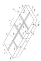
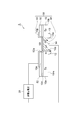
- FIG. 1 is a diagram schematically showing a configuration of an optical waveguide device according to an embodiment.
- the optical waveguide element 1 is, for example, a light modulation element, and includes a substrate 10 and a signal electrode 20.
- the substrate 10 is a plate-like member extending along one direction (hereinafter referred to as “direction A (first direction)”), and is, for example, electric such as lithium niobate (LiNbO 3 , hereinafter referred to as “LN”). It is comprised from the dielectric material (ferroelectric material) which has an optical effect.
- the length along the direction A of the substrate 10 is about 10 to 150 mm, for example, and the length along the direction orthogonal to the direction A of the substrate 10 (hereinafter referred to as “direction B”) is about 0.1 to 3 mm, for example.
- the thickness of the substrate 10 is, for example, about 0.2 to 1 mm.
- the substrate 10 includes an end surface 10a and an end surface 10b that are both end surfaces in the direction A, and a side end surface 10c and a side end surface 10d that are both end surfaces in the direction B.
- the substrate 10 has a first region 10e, a second region 10f, and a third region 10g.
- the first region 10e, the second region 10f, and the third region 10g are arranged in order along the direction A.
- the crystal material axis direction Z of the dielectric material is oriented in a direction opposite to the normal axis NV direction of the main surface 10m of the substrate 10, for example.
- the crystal material axis direction Z of the dielectric material is directed to the normal axis NV direction of the main surface 10m of the substrate 10, for example.
- the crystal axis direction Z of the dielectric material is directed in the direction opposite to the normal axis NV direction of the main surface 10m of the substrate 10, for example.
- the polarization direction of the dielectric is in the same direction as the crystal axis direction Z. That is, the polarization direction of the first region 10e is opposite to the polarization direction of the second region 10f, and the polarization direction of the first region 10e is the same as the polarization direction of the third region 10g.
- the substrate 10 includes a ridge portion 11 (first ridge portion), a ridge portion 12 (second ridge portion), a ridge portion 13 (third ridge portion), and a trench portion 14.
- the ridge portion 11 is provided on the main surface 10m and extends along the direction A from the end surface 10a to the end surface 10b.
- the cross-sectional shape orthogonal to the direction A of the ridge portion 11 has a trapezoidal shape.
- the width of the top of the ridge portion 11 is, for example, about 9 ⁇ m.
- the width of the bottom of the ridge portion 11 is about 12 ⁇ m, for example.
- the height of the ridge portion 11 is, for example, about 6 ⁇ m.
- a thickness Tr1 of the substrate 10 in the ridge portion 11 is, for example, about 1 mm.
- the ridge portion 11 includes an optical waveguide 11a.
- the optical waveguide 11a is a linear optical waveguide and extends along the direction A from the end surface 10a to the end surface 10b.
- the optical waveguide 11a is formed by doping the substrate 10 with an impurity such as titanium.
- the ridge portion 12 is provided on the domain wall D1 that is a boundary surface between the first region 10e and the second region 10f, and extends along the direction B from the side end surface 10c to the side end surface 10d.
- the domain wall D1 is located on the side surface 12a on the second region 10f side of both side surfaces of the ridge portion 12, and extends from the side surface 12a to the back surface 10n of the substrate 10.
- the cross-sectional shape orthogonal to the direction B of the ridge portion 12 has a trapezoidal shape.
- the width of the top of the ridge portion 12 is, for example, about 9 to 20 ⁇ m.
- the width of the bottom of the ridge portion 12 is, for example, about 12 to 23 ⁇ m when the ridge shape is trapezoidal and the base angle is 75 degrees.
- the height of the ridge portion 12 is, for example, about 6 ⁇ m.
- the thickness Tr2 of the substrate 10 in the ridge portion 12 is, for example, about 1 mm.
- the ridge portion 13 is provided on the domain wall D2 that is a boundary surface between the second region 10f and the third region 10g, and extends along the direction B from the side end surface 10c to the side end surface 10d.
- the domain wall D2 is located on the side surface 13a on the second region 10f side of both side surfaces of the ridge portion 13, and extends from the side surface 13a to the back surface 10n of the substrate 10.
- the cross-sectional shape orthogonal to the direction B of the ridge portion 13 has a trapezoidal shape.
- the width of the top of the ridge portion 13 is, for example, about 9 to 20 ⁇ m.
- the width of the bottom of the ridge portion 13 is, for example, about 12 to 23 ⁇ m when the ridge shape is trapezoidal and the base angle is 75 degrees.
- the height of the ridge portion 13 is, for example, about 6 ⁇ m.
- the thickness Tr3 of the substrate 10 in the ridge portion 13 is, for example, about 1 mm.
- the thickness of the unprocessed wafer may be uneven.
- the height of the ridge portion 12 and the ridge portion 13 may be larger than the flatness (TTV) of the wafer.
- TTV flatness
- the flatness of the wafer is the difference between the maximum value and the minimum value of the entire surface of the wafer measured in the thickness direction with the wafer back surface as the reference surface.
- the trench portion 14 is a portion sandwiched between the ridge portion 12 and the ridge portion 13, and is divided by the ridge portion 11 into the side end face 10c side and the side end face 10d side.
- the thickness Tt of the substrate 10 in the trench portion 14 may be a thickness obtained by subtracting the height of the ridge portion 12 from the thickness Tr2 of the substrate 10 in the ridge portion 12, for example.
- the signal electrode 20 is a long member for transmitting a modulation signal, which is an electric signal supplied from the outside, and applying an electric field corresponding to the modulation signal to the optical waveguide 11a.
- the signal electrode 20 is made of, for example, gold (Au).
- the signal electrode 20 includes a first portion 20a, a second portion 20b, a third portion 20c, and a fourth portion 20d.
- the first portion 20 a is provided on the main surface 10 m in the first region 10 e of the substrate 10.
- the first portion 20 a extends in the direction B from the side end surface 10 c of the substrate 10 to the ridge portion 11.
- One end of the first portion 20a is electrically connected to an external circuit for supplying a modulation signal.
- the second portion 20b is provided on the ridge portion 11 in the first region 10e, and extends in the direction A from the other end of the first portion 20a to the domain wall D1.
- One end of the second portion 20b is connected to the other end of the first portion 20a.
- the third portion 20c is provided on the ridge portion 11 in the second region 10f and extends in the direction A from the domain wall D1 to the domain wall D2. One end of the third portion 20c is connected to the other end of the second portion 20b.
- the second portion 20b and the third portion 20c function as an action portion that applies an electric field formed by the modulation signal to the optical waveguide 11a.
- the fourth portion 20d is provided on the ridge portion 13, and extends in the direction opposite to the direction B from the other end of the third portion 20c to the side end face 10c. One end of the fourth portion 20d is connected to the other end of the third portion 20c, and the other end of the fourth portion 20d is electrically connected to the termination circuit.
- the optical waveguide element 1 may further include a buffer layer (not shown).
- the buffer layer is provided on the substrate 10 and is located between the ridge portion 11 and the signal electrode 20 in the ridge portion 11.
- the buffer layer is provided to reduce absorption by the signal electrode 20 of light propagating through the optical waveguide 11a.
- the buffer layer is made of, for example, silicon oxide (for example, SiO 2 ).
- optical waveguide device 1 configured as described above, input light is input from the end face 10a to the optical waveguide 11a.
- the input light propagates through the optical waveguide 11a.
- the electric field formed by the modulation signal transmitted by the signal electrode 20 is applied to the optical waveguide 11a, whereby the refractive index of the optical waveguide 11a changes.
- the light propagating through the optical waveguide 11a is modulated according to the refractive index change of the optical waveguide 11a.
- the modulated light is output from the end face 10b as modulated light.
- the crystal axis direction Z of the dielectric material in the first region 10 e is directed in the direction opposite to the normal axis NV direction of the main surface 10 m of the substrate 10.
- the crystal axis direction Z of the dielectric material in the second region 10f is directed to the normal axis NV direction of the main surface 10m of the substrate 10. Therefore, in the first region 10e, the low-frequency induced phase amount increases in proportion to the length of the second portion 20b, and the high-frequency induced phase amount increases as the length of the second portion 20b increases. Increases moderately.
- the amount of change in the low-frequency and high-frequency induced phase amounts is the same as the amount of change in the low-frequency and high-frequency induced phase amounts in the first region 10e.
- the direction of change of the induced phase amount is opposite to the direction of change of the low-frequency and high-frequency induced phase amounts in the first region 10e. That is, in the second region 10f, the low-frequency induced phase amount decreases in proportion to the length of the second portion 20b, and the high-frequency induced phase amount gradually decreases as the length of the second portion 20b increases. To decrease. For this reason, the difference between the low-frequency induced phase amount and the high-frequency induced phase amount is reduced, and the optical frequency response characteristic is flattened. As a result, it is possible to increase the bandwidth.
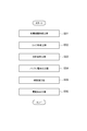
- FIG. 2 is a process diagram showing an example of a method for manufacturing the optical waveguide device 1.
- the method of manufacturing the optical waveguide device 1 includes an optical waveguide formation step S01, a ridge formation step S02, a polarization treatment step S03, a buffer layer formation step S04, a heat treatment step S05, and an electrode formation.
- Step S06 the method of manufacturing the optical waveguide device 1 includes an optical waveguide formation step S01, a ridge formation step S02, a polarization treatment step S03, a buffer layer formation step S04, a heat treatment step S05, and an electrode formation.
- the optical waveguide 11a is formed on the main surface 10m of the substrate 10 (wafer).
- the optical waveguide 11a is formed by doping impurities on the main surface 10m of the substrate 10 in a portion where the optical waveguide 11a is formed.
- impurities are deposited on the portion where the optical waveguide 11a is formed, and the deposited impurities are thermally diffused to dope the impurities.
- the impurity to be doped may be any impurity that lowers the coercive electric field Ec (also referred to as polarization inversion electric field) of the dielectric material included in the substrate 10, such as titanium (Ti), copper (Cu), chromium (Cr), etc. It is.
- the coercive electric field Ec is an electric field that reverses the polarization direction of the spontaneous polarization of the dielectric.
- the coercive electric field Ec of an LN crystal that is commercially available for an optical waveguide is about 21 kV / mm, but the coercive electric field Ect of an LN crystal doped with titanium is smaller than the coercive electric field Ec of an LN crystal.
- the ridge portion 11, the ridge portion 12, and the ridge portion 13 are formed on the main surface 10m of the substrate 10 on which the optical waveguide 11a is formed in the optical waveguide formation step S01.
- a mask M is formed so as to cover regions on the main surface 10m corresponding to the ridge portion 11, the ridge portion 12, and the ridge portion 13 by, for example, photolithography. .
- FIG. 3 is a plan view schematically showing the configuration of the substrate 10 on which the mask M is formed in the ridge formation step S02.
- the mask M is formed on the main surface 10 m of the substrate 10 so as to cover a portion where the ridge portion 11, the ridge portion 12 and the ridge portion 13 are formed.
- the main surface 10m of the substrate 10 is chemically removed by dry etching, wet etching, or the like, thereby forming the ridge portion 11, the ridge portion 12, and the ridge portion 13.
- the ridge portion 11, the ridge portion 12, and the ridge portion 13 may be formed by mechanically removing the main surface 10m of the substrate 10 by sandblasting, cutting, or the like.
- the mask M is removed.
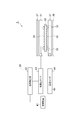
- the polarization inverting device 3 includes a sandwiching member 31, a sealing member 32, a liquid electrode 33, a liquid electrode 34, a high voltage power supply 35, a polarizer 36, and an analyzer 37.
- the clamping member 31 is a pair of plate-like members for clamping the substrate 50, and is a transparent resin plate such as an acrylic plate.
- the sealing member 32 is, for example, an annular resin material (O-ring).
- the liquid electrode 33 and the liquid electrode 34 are conductive liquids, for example, lithium chloride (LiCl) aqueous solutions.
- the polarizer 36 and the analyzer 37 are polarizing plates for observing a crossed Nicol image.
- the high voltage power supply 35 is a device for supplying a high voltage.
- the high voltage power supply 35 includes a control device 41, a signal generator 42, a high voltage amplifier 43, and a current monitor 44.
- the control device 41 is a PC (Personal Computer), for example, and transmits a control signal to the signal generator 42 according to the current monitored by the current monitor 44.
- the signal generator 42 is, for example, a pulse generator, and outputs a pulse signal having a voltage of several volts in accordance with the control signal output from the control device 41.
- the high voltage amplifier 43 is a circuit that amplifies the voltage, and amplifies the voltage of the pulse signal output from the signal generator 42.
- the high voltage amplifier 43 outputs the amplified pulse signal to the liquid electrode 34 and applies the high voltage V between the liquid electrode 33 and the liquid electrode 34.
- the current monitor 44 monitors the current flowing through the substrate 10.
- the substrate 50 is sandwiched by the pair of sandwiching members 31 via the sealing member 32, and the liquid electrode is interposed between the one surface of the substrate 50 and the sandwiching member 31. 33 is filled, and the liquid electrode 34 is filled between the other surface of the substrate 50 and the sandwiching member 31.
- the high voltage power source 35 generates a signal by the signal generator 42 based on the control signal from the control device 41, and the high voltage V between the liquid electrode 33 and the liquid electrode 34 via the high voltage amplifier 43. Apply.
- the control device 41 When the control device 41 detects that the charge amount obtained by time integration of the current monitored by the current monitor 44 has reached a value determined according to the area of the region to be inverted, the control device 41 outputs a signal to the signal generator 42. Stop.
- substrate 50 clamped by the clamping member 31 is the board
- FIG. 5 is a diagram schematically showing an example of a masking method for the substrate 10 in the polarization inverting device 3.
- the substrate 50 includes the substrate 10 and a mask layer 51 provided on the main surface 10 m of the substrate 10.
- the mask layer 51 has an insulating property, and is made of, for example, an insulating resin.
- Mask layer 51 is provided on main surface 10 m so as to cover a portion from end surface 10 a of substrate 10 to the top surface of ridge portion 12 and a portion from end surface 10 b to the top surface of ridge portion 13.
- the mask layer 51 has an opening 51 a on a portion of the main surface 10 m sandwiched between the top surface of the ridge portion 12 and the top surface of the ridge portion 13.
- the mask layer 51 can be formed by, for example, spin coating or photolithography.
- the thickness Tr1, the thickness Tr2, and the thickness Tr3 are all described as the thickness Tr.
- a voltage V is supplied between the liquid electrode 33 and the liquid electrode 34. At this time, the voltage V is applied to the substrate 10 through the opening 51 a of the mask layer 51.
- the electric field Er in the ridge portion 12 and the ridge portion 13 is a value (V / Tr) obtained by dividing the voltage V by the thickness Tr of the substrate 10 in the ridge portion 12 and the ridge portion 13.
- the electric field Et in the trench portion 14 is a value (V / Tt) obtained by dividing the voltage V by the thickness Tt of the substrate 10 in the trench portion 14.
- the voltage V is adjusted so that the coercive electric field Ec of the substrate 10 is between the electric field Er and the electric field Et (Er ⁇ Ec ⁇ Et).
- the electric field in the ridge portion 11 is equal to the electric field Er on average.
- the coercive electric field Ect in the ridge portion 11 is smaller than the coercive electric field Ec, so that the polarization inversion can be performed by the electric field Er.
- the electric field Ep at the position where the mask layer 51 is provided is smaller than the electric field Er. For this reason, the polarization direction of the region sandwiched between the ridge portion 12 and the ridge portion 13 of the substrate 10 is reversed to form the second region 10f.
- a buffer layer is formed at 10 m.
- a buffer layer may be formed on the main surface 10m of the substrate 10 so as to cover the entire main surface 10m.
- the buffer layer is formed by a general-purpose thin film deposition method such as a vacuum deposition method, an ion-assisted vacuum deposition method, a sputtering method, and a CVD (chemical vapor deposition) method.
- the buffer layer is made of, for example, silicon oxide (SiO 2 ) or aluminum oxide (Al 2 O 3 ).
- the buffer layer is subjected to a heat treatment in order to compensate for oxygen vacancies in the buffer layer formed in the buffer layer formation step S04.
- This heat treatment is performed at a temperature of about 600 degrees in an oxygen-containing atmosphere.
- the signal electrode 20 is formed on the buffer layer. More specifically, a resist pattern is formed on the buffer layer by photolithography. This resist pattern has an opening for the signal electrode 20. Next, the signal electrode 20 is formed on the buffer layer using, for example, a plating method using the resist pattern as a mask. In the electrode formation step S06, a ground electrode may be formed on the buffer layer. After the signal electrode 20 is formed, the resist pattern is removed.
- the buffer layer formation step S04 and the heat treatment step S05 may be performed between the ridge formation step S02 and the polarization treatment step S03, and may be omitted when no buffer layer is provided.
- the substrate 10 is doped with an impurity that lowers the coercive electric field Ec of the substrate 10 to form the optical waveguide 11a extending in the direction A, and the ridge extending in the direction A including the optical waveguide 11a.
- a ridge portion 12 and a ridge portion 13 intersecting with the portion 11 and the ridge portion 11 are formed.
- a voltage V is applied to a region of the substrate 10 sandwiched between the ridge portion 12 and the ridge portion 13 (one region divided by the ridge portion 12).
- the electric field Et generated in the trench portion 14 is larger than the electric field Er generated in the ridge portion 12 and the ridge portion 13.
- the polarization direction is reversed by adjusting the voltage V so that the coercive electric field Ec of the substrate 10 is larger than the electric field Er generated in the ridge portion 12 and the ridge portion 13 and smaller than the electric field Et generated in the trench portion 14.
- the spread of the second region 10 f can be limited by the ridge portion 12 and the ridge portion 13.
- the second region 10 f is formed to extend to the side surface 12 a of the ridge portion 12 in the direction opposite to the direction A, but is not formed beyond the ridge portion 12. Further, the second region 10f is formed to extend to the side surface 13a of the ridge portion 13 in the direction A, but is not formed beyond the ridge portion 13. In this way, it is possible to prevent polarization inversion beyond the ridge portion 12 and the ridge portion 13. Further, since the ridge portion 11 contains impurities that lower the coercive electric field Ec of the substrate 10, the polarization direction of the ridge portion 11 sandwiched between the ridge portion 12 and the ridge portion 13 can be reversed. As a result, it is possible to improve the accuracy of the polarization inversion process of the substrate 10.
- the following phenomenon occurs under the condition that the polarization inversion of the ridge portion 11 can be stably inverted with good reproducibility.
- the voltage V is applied to the region sandwiched between the ridge portion 12 and the ridge portion 13 using the liquid electrodes 33 and 34. For this reason, the substrate 10 and the liquid electrodes 33 and 34 can be reliably contacted, and the uniformity of the voltage applied to the substrate 10 can be improved. As a result, the accuracy of the polarization inversion process can be further improved.
- the manufacturing method of the optical waveguide device and the optical waveguide device according to one aspect of the present invention is not limited to the above embodiment.
- the optical waveguide element 1 is not limited to an optical modulation element, and may be an optical switch, a polarization controller, or the like.
- the ridge portion 12 and the ridge portion 13 may be appropriately changed depending on the shape that forms the polarization inversion.
- the optical waveguide cannot be composed of only a straight portion, and is skewed or bent.
- the portion is a ridge waveguide
- the ridge portion 12 and the ridge portion 13 may not be perpendicular to the direction A and may be inclined.
- the region where the polarization is reversed does not include the end surface 10a, the end surface 10b, the side end surface 10c and the side end surface 10d, that is, when the region is closed in the substrate 10, a ridge portion may be provided so as to surround the region where the polarization is reversed. Good.
- a ridge portion intersecting with the direction B may be provided, and the regions may be divided so that the polarization directions are different between the optical waveguides.
- the optical waveguide 11a may be a Mach-Zehnder type optical waveguide or may have a structure corresponding to the modulation method of the optical waveguide element 1.
- the substrate 10 includes the first region 10e and the second region 10f, and may not include the third region 10g.
- the optical waveguide element 1 may not have the ridge portion 13.
- the number of the regions is not limited as long as the substrate 10 has two or more regions arranged in order along the direction A.
- the polarization directions of adjacent regions are opposite to each other, and the substrate 10 only needs to have a ridge portion provided on the domain wall (boundary surface) of the adjacent region.
- the flatness of the substrate 10 on which the optical waveguide 11a is formed is measured, and the ridge portion 12 and the ridge portion 12 so that the heights of the ridge portion 12 and the ridge portion 13 are larger than the flatness of the substrate 10.
- the ridge portion 13 may be formed.
- FIG. 6 is an enlarged view schematically showing the periphery of the trench portion in the substrate of the comparative example.
- the back surface 110 n is expanded, and the height of the ridge portion 112 and the ridge portion 113 is smaller than the flatness of the substrate 110. That is, the thickness Tt of the substrate 110 in the trench portion 114 is larger than the thickness Tr of the substrate 110 in the ridge portion 112 and the ridge portion 113.
- the polarization directions of the ridge portion 112 and the ridge portion 113 are reversed, and the polarization may be reversed beyond the ridge portion 112 and the ridge portion 113.
- the height of the ridge portion 12 and the ridge portion 13 is larger than the flatness of the substrate 10. That is, the thickness Tr of the substrate 10 in the ridge portion 12 and the ridge portion 13 is larger than the thickness Tt of the substrate 10 in the trench portion 14.
- the voltage V is increased to make the electric field Et of the trench portion 14 larger than the coercive electric field Ec of the substrate 10.
- the coercive electric field Ec of the substrate 10 becomes the electric field Er and the electric field Et.
- the voltage V can be adjusted to be between (Er ⁇ Ec ⁇ Et). For this reason, the range of the substrate 10 whose polarization is inverted can be limited by the ridge portion 12 and the ridge portion 13. Thus, in the substrate 10, it is possible to improve the certainty of control of polarization inversion by the ridge portion 12 and the ridge portion 13. As a result, the accuracy of the polarization inversion process can be further improved.
- the masking method of the substrate 10 in the polarization inverting device 3 is not limited to the above-described method. Below, the modification of the masking method of the board
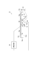
- FIG. 7 is a diagram schematically showing a first modification of the masking method for the substrate 10 in the polarization inverting device 3.
- the substrate 50 is different from the substrate 50 of FIG. 5 in that a mask layer 52 is provided instead of the mask layer 51. That is, in the substrate 50 of FIG. 7, the mask layer 52 is formed on the back surface 10 n of the substrate 10 from the end surface 10 a of the substrate 10 to a position facing the ridge portion 12 and from the end surface 10 b to the position facing the ridge portion 13. Is provided on the back surface 10n so as to cover the portion.
- the mask layer 52 has an opening 52a on a portion of the back surface 10n sandwiched between a position facing the ridge portion 12 and a position facing the ridge portion 13.
- the mask layer 52 has an insulating property, and is made of, for example, an insulating resin.
- the mask layer 52 can be formed by, for example, spin coating or photolithography.
- This polarization inversion device 3 can also invert the polarization direction of a desired region of the substrate 10 in the same manner as the polarization inversion device 3 of FIG. Further, since the insulating resin (mask layer 52) formed by photolithography or the like is not scattered by the ridge portion 11, the ridge portion 12, and the ridge portion 13, the domain inversion boundaries (domain wall D1 and domain wall D2). ) Can be formed sharply and accurately.
- FIG. 8 is a diagram schematically showing a second modification of the masking method for the substrate 10 in the polarization inverting device 3.
- the substrate 50 is different from the substrate 50 of FIG. 7 in that a metal film 53 is further provided. That is, in the substrate 50 of FIG. 8, the metal film 53 is provided on the mask layer 52 in a range surrounded by the sealing member 32.
- the metal film 53 is provided on the back surface 10 n of the substrate 10 in the opening 52 a and is in contact with the substrate 10.
- the metal film 53 has conductivity and is made of, for example, chromium (Cr), aluminum (Al), gold (Au), or the like.
- the metal film 53 can be formed by, for example, a lift-off method.
- This polarization inversion device 3 can also invert the polarization direction of a desired region of the substrate 10 in the same manner as the polarization inversion device 3 of FIG. Further, by using the metal film 53, the uniformity of the applied electric field can be improved.
- FIG. 9 is a diagram schematically showing a third modification of the masking method for the substrate 10 in the polarization inverting device 3.
- the polarization inverting device 3 does not include the clamping member 31, the sealing member 32, the liquid electrode 33, and the liquid electrode 34, and thus the polarization inverting device 3 of FIGS. 5, 7, and 8. Is different.
- the substrate 50 is different from the substrate 50 of FIG. 5 in that a metal film 54 and a metal film 55 are provided instead of the mask layer 51. 9, the metal film 54 is provided on the main surface 10m of the substrate 10 between the ridge portion 12 and the ridge portion 13, and the metal film 54 is provided on the back surface 10n of the substrate 10.
- a metal film 55 is provided so as to cover the opposing portions.
- the metal film 54 and the metal film 55 have conductivity and are made of, for example, Cr, Al, Au, or the like.
- the metal film 54 and the metal film 55 can be formed by, for example, a lift-off method.
- This polarization inversion device 3 can also invert the polarization direction of a desired region of the substrate 10 in the same manner as the polarization inversion device 3 of FIG. Further, by using the metal film 54 and the metal film 55, the uniformity of the applied electric field can be improved. Further, the liquid electrode 33 and the liquid electrode 34 do not leak, and the polarization can be easily reversed.
- FIG. 10 is a diagram schematically showing a fourth modification of the masking method for the substrate 10 in the polarization inverting device 3.
- the polarization inverting device 3 does not include the clamping member 31, the sealing member 32, the liquid electrode 33, and the liquid electrode 34, and thus the polarization inverting device 3 of FIGS. 5, 7, and 8. Is different.
- the substrate 50 further differs from the substrate 50 of FIG. 8 in that it further includes a metal film 54.
- This polarization inversion device 3 can also invert the polarization direction of a desired region of the substrate 10 in the same manner as the polarization inversion device 3 of FIG. Further, the liquid electrode 33 and the liquid electrode 34 do not leak, and the polarization can be easily reversed.
- SYMBOLS 1 Optical waveguide element, 10 ... Board
Landscapes
- Physics & Mathematics (AREA)
- Nonlinear Science (AREA)
- General Physics & Mathematics (AREA)
- Optics & Photonics (AREA)
- Engineering & Computer Science (AREA)
- Microelectronics & Electronic Packaging (AREA)
- Chemical & Material Sciences (AREA)
- Ceramic Engineering (AREA)
- Crystallography & Structural Chemistry (AREA)
- Optical Modulation, Optical Deflection, Nonlinear Optics, Optical Demodulation, Optical Logic Elements (AREA)
- Optical Integrated Circuits (AREA)
Abstract
Description
図7は、分極反転装置3における基板10のマスキング方法の第1変形例を概略的に示す図である。図7に示されるように、基板50は、マスク層51に代えてマスク層52を備えている点で、図5の基板50と相違する。すなわち、図7の基板50では、マスク層52は、基板10の裏面10nのうち基板10の端面10aからリッジ部12に対向する位置までの部分と、端面10bからリッジ部13に対向する位置までの部分と、を覆うように裏面10nに設けられている。マスク層52は、裏面10nのうちリッジ部12に対向する位置とリッジ部13に対向する位置とに挟まれた部分の上に開口52aを有している。マスク層52は、絶縁性を有し、例えば絶縁性樹脂から構成されている。マスク層52は、例えばスピンコートまたはフォトリソグラフィにより形成され得る。
図8は、分極反転装置3における基板10のマスキング方法の第2変形例を概略的に示す図である。図8に示されるように、基板50は、金属膜53がさらに設けられている点で、図7の基板50と相違する。すなわち、図8の基板50では、金属膜53は、封止部材32に囲まれた範囲において、マスク層52上に設けられている。金属膜53は、開口52aにおいて基板10の裏面10nに設けられ、基板10と接触を成している。金属膜53は、導電性を有し、例えばクロム(Cr)、アルミニウム(Al)、金(Au)等から構成されている。金属膜53は、例えばリフトオフ法により形成され得る。
図9は、分極反転装置3における基板10のマスキング方法の第3変形例を概略的に示す図である。図9に示されるように、分極反転装置3は、挟持部材31、封止部材32、液体電極33及び液体電極34を備えていない点で、図5、図7、図8の分極反転装置3と相違する。基板50は、マスク層51に代えて、金属膜54及び金属膜55を備えている点で図5の基板50と相違する。すなわち、図9の基板50では、基板10の主面10mのうち、リッジ部12とリッジ部13とに挟まれた部分に金属膜54が設けられ、基板10の裏面10nのうち金属膜54に対向する部分を覆うように金属膜55が設けられている。金属膜54及び金属膜55は、導電性を有し、例えばCr、Al、Au等から構成されている。金属膜54及び金属膜55は、例えばリフトオフ法により形成され得る。
図10は、分極反転装置3における基板10のマスキング方法の第4変形例を概略的に示す図である。図10に示されるように、分極反転装置3は、挟持部材31、封止部材32、液体電極33及び液体電極34を備えていない点で、図5、図7、図8の分極反転装置3と相違する。基板50は、さらに金属膜54を備えている点で、図8の基板50と相違する。
Claims (6)
- 基板の抗電界を下げる不純物をドープすることによって、第1方向に延びる光導波路を前記基板に形成する光導波路形成工程と、
前記光導波路を含む第1リッジ部及び前記第1リッジ部と交差する第2リッジ部を形成するリッジ形成工程と、
前記基板のうち、前記第2リッジ部によって区分される一方の領域に電圧を印加することにより、前記領域の分極方向を反転する分極処理工程と、
を備える光導波路素子の製造方法。 - 前記リッジ形成工程において、前記第2リッジ部の高さが前記基板の平坦度より大きくなるように、前記第2リッジ部を形成する、請求項1に記載の光導波路素子の製造方法。
- 前記分極処理工程において、液体電極を用いて前記領域に電圧を印加する、請求項1または請求項2に記載の光導波路素子の製造方法。
- 前記リッジ形成工程において、前記第1リッジ部と交差する第3リッジ部をさらに形成し、
前記分極処理工程において、前記基板のうち、前記第2リッジ部と前記第3リッジ部とに挟まれる領域に電圧を印加することにより、前記領域の分極方向を反転する、請求項1~請求項3のいずれか一項に記載の光導波路素子の製造方法。 - 第1方向に延びる第1リッジ部と、前記第1リッジ部と交差する第2リッジ部と、を有する基板を備え、
前記第1リッジ部は、前記第1方向に延びる光導波路を有し、
前記光導波路は、前記基板の抗電界を下げる不純物を含んでおり、
前記基板は、前記第1方向に沿って順に配置された第1領域及び第2領域を有し、
前記第1領域の分極方向は、前記第2領域の分極方向と反対であり、
前記第2リッジ部は、前記第1領域と前記第2領域との境界上に設けられている、光導波路素子。 - 前記第2リッジ部の高さは、前記基板の平坦度より大きい、請求項5に記載の光導波路素子。
Priority Applications (3)
| Application Number | Priority Date | Filing Date | Title |
|---|---|---|---|
| US14/768,699 US9348156B2 (en) | 2013-02-21 | 2014-02-19 | Optical waveguide element and method for manufacturing optical waveguide element |
| CN201480009860.XA CN105074545B (zh) | 2013-02-21 | 2014-02-19 | 光波导元件以及光波导元件的制造方法 |
| JP2014510599A JP6015749B2 (ja) | 2013-02-21 | 2014-02-19 | 光導波路素子及び光導波路素子の製造方法 |
Applications Claiming Priority (2)
| Application Number | Priority Date | Filing Date | Title |
|---|---|---|---|
| JP2013-032058 | 2013-02-21 | ||
| JP2013032058 | 2013-02-21 |
Publications (1)
| Publication Number | Publication Date |
|---|---|
| WO2014129508A1 true WO2014129508A1 (ja) | 2014-08-28 |
Family
ID=51391294
Family Applications (1)
| Application Number | Title | Priority Date | Filing Date |
|---|---|---|---|
| PCT/JP2014/053943 Ceased WO2014129508A1 (ja) | 2013-02-21 | 2014-02-19 | 光導波路素子及び光導波路素子の製造方法 |
Country Status (4)
| Country | Link |
|---|---|
| US (1) | US9348156B2 (ja) |
| JP (1) | JP6015749B2 (ja) |
| CN (1) | CN105074545B (ja) |
| WO (1) | WO2014129508A1 (ja) |
Cited By (1)
| Publication number | Priority date | Publication date | Assignee | Title |
|---|---|---|---|---|
| CN110325900A (zh) * | 2016-12-02 | 2019-10-11 | 洛克利光子有限公司 | 波导光电器件 |
Families Citing this family (1)
| Publication number | Priority date | Publication date | Assignee | Title |
|---|---|---|---|---|
| CN112636166B (zh) * | 2020-12-18 | 2022-03-15 | 中国科学院半导体研究所 | 一种可调谐单纵模激光器及其制备方法 |
Citations (5)
| Publication number | Priority date | Publication date | Assignee | Title |
|---|---|---|---|---|
| JPH112848A (ja) * | 1997-06-12 | 1999-01-06 | Mitsubishi Cable Ind Ltd | 分極反転結晶の製造方法 |
| US6156255A (en) * | 1994-09-16 | 2000-12-05 | The Board Of Trustees Of The Leland Stanford, Jr. University | Electric field domain patterning |
| JP2005292287A (ja) * | 2004-03-31 | 2005-10-20 | Sumitomo Osaka Cement Co Ltd | 分極反転形成方法 |
| WO2009004683A1 (ja) * | 2007-06-29 | 2009-01-08 | Fujitsu Limited | 光変調器および波長チャープ切替方法 |
| JP2010078914A (ja) * | 2008-09-26 | 2010-04-08 | Fujitsu Ltd | 光機能デバイス |
Family Cites Families (11)
| Publication number | Priority date | Publication date | Assignee | Title |
|---|---|---|---|---|
| US5519802A (en) * | 1994-05-09 | 1996-05-21 | Deacon Research | Method for making devices having a pattern poled structure and pattern poled structure devices |
| US6356673B1 (en) | 2000-05-05 | 2002-03-12 | The United States Of America As Represented By The Secretary Of The Navy | Low loss coplanar waveguide horn for low drive LiNbO3 modulators |
| US6999668B2 (en) * | 2002-01-09 | 2006-02-14 | Matsushita Electric Industrial Co., Ltd. | Method for manufacturing optical waveguide device, optical waveguide device, and coherent light source and optical apparatus using the optical waveguide device |
| JP2003262841A (ja) | 2002-03-07 | 2003-09-19 | Fujitsu Ltd | 光変調装置及び設計方法 |
| CN100390651C (zh) * | 2002-11-25 | 2008-05-28 | 松下电器产业株式会社 | 光学元件的制造方法和具有极化反转结构的光学元件 |
| US8193004B2 (en) * | 2004-03-18 | 2012-06-05 | Sumitomo Osaka Cement Co., Ltd. | Method for forming ferroelectric spontaneous polarization reversal |
| JP3924289B2 (ja) * | 2004-03-30 | 2007-06-06 | 住友大阪セメント株式会社 | 光変調素子及びその製造方法 |
| JP2006343410A (ja) * | 2005-06-07 | 2006-12-21 | Nippon Telegr & Teleph Corp <Ntt> | ポラリトン導波路 |
| JP2008116865A (ja) | 2006-11-08 | 2008-05-22 | Sumitomo Osaka Cement Co Ltd | ネスト型変調器 |
| CN101535887B (zh) * | 2006-11-09 | 2012-06-20 | 日本碍子株式会社 | 光波导基板的制造方法 |
| US20140079351A1 (en) | 2012-09-20 | 2014-03-20 | Phase Sensitive Innovations, Inc | Millimeter-wave electro-optic modulator |
-
2014
- 2014-02-19 WO PCT/JP2014/053943 patent/WO2014129508A1/ja not_active Ceased
- 2014-02-19 CN CN201480009860.XA patent/CN105074545B/zh not_active Expired - Fee Related
- 2014-02-19 JP JP2014510599A patent/JP6015749B2/ja not_active Expired - Fee Related
- 2014-02-19 US US14/768,699 patent/US9348156B2/en not_active Expired - Fee Related
Patent Citations (5)
| Publication number | Priority date | Publication date | Assignee | Title |
|---|---|---|---|---|
| US6156255A (en) * | 1994-09-16 | 2000-12-05 | The Board Of Trustees Of The Leland Stanford, Jr. University | Electric field domain patterning |
| JPH112848A (ja) * | 1997-06-12 | 1999-01-06 | Mitsubishi Cable Ind Ltd | 分極反転結晶の製造方法 |
| JP2005292287A (ja) * | 2004-03-31 | 2005-10-20 | Sumitomo Osaka Cement Co Ltd | 分極反転形成方法 |
| WO2009004683A1 (ja) * | 2007-06-29 | 2009-01-08 | Fujitsu Limited | 光変調器および波長チャープ切替方法 |
| JP2010078914A (ja) * | 2008-09-26 | 2010-04-08 | Fujitsu Ltd | 光機能デバイス |
Cited By (2)
| Publication number | Priority date | Publication date | Assignee | Title |
|---|---|---|---|---|
| CN110325900A (zh) * | 2016-12-02 | 2019-10-11 | 洛克利光子有限公司 | 波导光电器件 |
| CN110325900B (zh) * | 2016-12-02 | 2023-11-17 | 洛克利光子有限公司 | 波导光电器件 |
Also Published As
| Publication number | Publication date |
|---|---|
| US9348156B2 (en) | 2016-05-24 |
| JP6015749B2 (ja) | 2016-10-26 |
| CN105074545B (zh) | 2018-06-22 |
| JPWO2014129508A1 (ja) | 2017-02-02 |
| CN105074545A (zh) | 2015-11-18 |
| US20160004105A1 (en) | 2016-01-07 |
Similar Documents
| Publication | Publication Date | Title |
|---|---|---|
| US10585328B2 (en) | Optical waveguide element and optical modulator using the same | |
| US10359684B2 (en) | Optical waveguide element and optical modulator using the same | |
| CN1113265C (zh) | 集成光学强度调制器及其制造方法 | |
| US6760493B2 (en) | Coplanar integrated optical waveguide electro-optical modulator | |
| US9244296B2 (en) | Optical modulator | |
| EP1271220A1 (en) | Coplanar integrated optical waveguide electro-optical modulator | |
| US7079714B2 (en) | Electro-optic devices having flattened frequency response with reduced drive voltage | |
| JP2011209629A (ja) | 導波路型偏光子 | |
| WO2018016428A1 (ja) | 誘電体薄膜付き基板およびこれを用いた光変調素子 | |
| CN1282028C (zh) | 宽带电光调制器 | |
| US12204184B2 (en) | Structure for an optoelectronics platform and method of fabricating a structure for an optoelectronics platform | |
| CN115268123A (zh) | 一种电调光波导相位调制器及相位调制方法 | |
| JP6015749B2 (ja) | 光導波路素子及び光導波路素子の製造方法 | |
| US20040207903A1 (en) | Electric field poling of ferroelectric materials | |
| US6195191B1 (en) | Optical devices having improved temperature stability | |
| US11947147B2 (en) | Optical device with microcrack resistance from surface roughness thereby reducing loss of light | |
| US7088874B2 (en) | Electro-optic devices, including modulators and switches | |
| US20220317371A1 (en) | Optical modulator | |
| Chelladurai et al. | 200 Gbit/s barium titanate modulator using weakly guided plasmonic modes | |
| Vasudevan et al. | Multi-domain Study of Oriented Thin-film Barium Titanate | |
| CN120871471A (zh) | 一种基于多维动态可调谐的铌酸锂电光调制器及其制备方法和应用 | |
| CN116931298A (zh) | 光学器件与光调制器 | |
| Lu et al. | Application of periodically-poled LiNbO/sub 3/for wide-bandwidth high-frequency electrooptic modulator | |
| EP1273960A1 (en) | Integrated ferroelectric optical waveguide device | |
| JP2004333949A (ja) | 光導波路型素子 |
Legal Events
| Date | Code | Title | Description |
|---|---|---|---|
| WWE | Wipo information: entry into national phase |
Ref document number: 201480009860.X Country of ref document: CN |
|
| ENP | Entry into the national phase |
Ref document number: 2014510599 Country of ref document: JP Kind code of ref document: A |
|
| 121 | Ep: the epo has been informed by wipo that ep was designated in this application |
Ref document number: 14754122 Country of ref document: EP Kind code of ref document: A1 |
|
| WWE | Wipo information: entry into national phase |
Ref document number: 14768699 Country of ref document: US |
|
| NENP | Non-entry into the national phase |
Ref country code: DE |
|
| 122 | Ep: pct application non-entry in european phase |
Ref document number: 14754122 Country of ref document: EP Kind code of ref document: A1 |