WO2014123050A1 - 表示装置の製造方法 - Google Patents
表示装置の製造方法 Download PDFInfo
- Publication number
- WO2014123050A1 WO2014123050A1 PCT/JP2014/051993 JP2014051993W WO2014123050A1 WO 2014123050 A1 WO2014123050 A1 WO 2014123050A1 JP 2014051993 W JP2014051993 W JP 2014051993W WO 2014123050 A1 WO2014123050 A1 WO 2014123050A1
- Authority
- WO
- WIPO (PCT)
- Prior art keywords
- light emitting
- emitting layer
- vapor deposition
- pixel
- opening
- Prior art date
- Legal status (The legal status is an assumption and is not a legal conclusion. Google has not performed a legal analysis and makes no representation as to the accuracy of the status listed.)
- Ceased
Links
Images







Classifications
-
- C—CHEMISTRY; METALLURGY
- C23—COATING METALLIC MATERIAL; COATING MATERIAL WITH METALLIC MATERIAL; CHEMICAL SURFACE TREATMENT; DIFFUSION TREATMENT OF METALLIC MATERIAL; COATING BY VACUUM EVAPORATION, BY SPUTTERING, BY ION IMPLANTATION OR BY CHEMICAL VAPOUR DEPOSITION, IN GENERAL; INHIBITING CORROSION OF METALLIC MATERIAL OR INCRUSTATION IN GENERAL
- C23C—COATING METALLIC MATERIAL; COATING MATERIAL WITH METALLIC MATERIAL; SURFACE TREATMENT OF METALLIC MATERIAL BY DIFFUSION INTO THE SURFACE, BY CHEMICAL CONVERSION OR SUBSTITUTION; COATING BY VACUUM EVAPORATION, BY SPUTTERING, BY ION IMPLANTATION OR BY CHEMICAL VAPOUR DEPOSITION, IN GENERAL
- C23C14/00—Coating by vacuum evaporation, by sputtering or by ion implantation of the coating forming material
- C23C14/22—Coating by vacuum evaporation, by sputtering or by ion implantation of the coating forming material characterised by the process of coating
- C23C14/24—Vacuum evaporation
-
- C—CHEMISTRY; METALLURGY
- C23—COATING METALLIC MATERIAL; COATING MATERIAL WITH METALLIC MATERIAL; CHEMICAL SURFACE TREATMENT; DIFFUSION TREATMENT OF METALLIC MATERIAL; COATING BY VACUUM EVAPORATION, BY SPUTTERING, BY ION IMPLANTATION OR BY CHEMICAL VAPOUR DEPOSITION, IN GENERAL; INHIBITING CORROSION OF METALLIC MATERIAL OR INCRUSTATION IN GENERAL
- C23C—COATING METALLIC MATERIAL; COATING MATERIAL WITH METALLIC MATERIAL; SURFACE TREATMENT OF METALLIC MATERIAL BY DIFFUSION INTO THE SURFACE, BY CHEMICAL CONVERSION OR SUBSTITUTION; COATING BY VACUUM EVAPORATION, BY SPUTTERING, BY ION IMPLANTATION OR BY CHEMICAL VAPOUR DEPOSITION, IN GENERAL
- C23C14/00—Coating by vacuum evaporation, by sputtering or by ion implantation of the coating forming material
- C23C14/04—Coating on selected surface areas, e.g. using masks
-
- H—ELECTRICITY
- H10—SEMICONDUCTOR DEVICES; ELECTRIC SOLID-STATE DEVICES NOT OTHERWISE PROVIDED FOR
- H10K—ORGANIC ELECTRIC SOLID-STATE DEVICES
- H10K59/00—Integrated devices, or assemblies of multiple devices, comprising at least one organic light-emitting element covered by group H10K50/00
- H10K59/30—Devices specially adapted for multicolour light emission
- H10K59/35—Devices specially adapted for multicolour light emission comprising red-green-blue [RGB] subpixels
-
- H—ELECTRICITY
- H10—SEMICONDUCTOR DEVICES; ELECTRIC SOLID-STATE DEVICES NOT OTHERWISE PROVIDED FOR
- H10K—ORGANIC ELECTRIC SOLID-STATE DEVICES
- H10K71/00—Manufacture or treatment specially adapted for the organic devices covered by this subclass
-
- H—ELECTRICITY
- H10—SEMICONDUCTOR DEVICES; ELECTRIC SOLID-STATE DEVICES NOT OTHERWISE PROVIDED FOR
- H10K—ORGANIC ELECTRIC SOLID-STATE DEVICES
- H10K71/00—Manufacture or treatment specially adapted for the organic devices covered by this subclass
- H10K71/10—Deposition of organic active material
- H10K71/16—Deposition of organic active material using physical vapour deposition [PVD], e.g. vacuum deposition or sputtering
- H10K71/164—Deposition of organic active material using physical vapour deposition [PVD], e.g. vacuum deposition or sputtering using vacuum deposition
-
- H—ELECTRICITY
- H10—SEMICONDUCTOR DEVICES; ELECTRIC SOLID-STATE DEVICES NOT OTHERWISE PROVIDED FOR
- H10K—ORGANIC ELECTRIC SOLID-STATE DEVICES
- H10K71/00—Manufacture or treatment specially adapted for the organic devices covered by this subclass
- H10K71/10—Deposition of organic active material
- H10K71/16—Deposition of organic active material using physical vapour deposition [PVD], e.g. vacuum deposition or sputtering
- H10K71/166—Deposition of organic active material using physical vapour deposition [PVD], e.g. vacuum deposition or sputtering using selective deposition, e.g. using a mask
-
- H—ELECTRICITY
- H10—SEMICONDUCTOR DEVICES; ELECTRIC SOLID-STATE DEVICES NOT OTHERWISE PROVIDED FOR
- H10K—ORGANIC ELECTRIC SOLID-STATE DEVICES
- H10K50/00—Organic light-emitting devices
- H10K50/10—OLEDs or polymer light-emitting diodes [PLED]
- H10K50/11—OLEDs or polymer light-emitting diodes [PLED] characterised by the electroluminescent [EL] layers
-
- H—ELECTRICITY
- H10—SEMICONDUCTOR DEVICES; ELECTRIC SOLID-STATE DEVICES NOT OTHERWISE PROVIDED FOR
- H10K—ORGANIC ELECTRIC SOLID-STATE DEVICES
- H10K71/00—Manufacture or treatment specially adapted for the organic devices covered by this subclass
- H10K71/10—Deposition of organic active material
- H10K71/16—Deposition of organic active material using physical vapour deposition [PVD], e.g. vacuum deposition or sputtering
Definitions
- the present invention relates to a method for manufacturing a display device.
- a full-color organic EL (Electroluminescence) display device is generally formed by arranging red (R), green (G), and blue (B) organic EL elements as sub-pixels on a substrate. By using these, the organic EL elements are selectively made to emit light with a desired luminance to display an image.
- R red
- G green
- B blue
- a light emitting layer made of an organic light emitting material that emits light of each color is patterned for each organic EL element that is a light emitting element.
- a method for forming a pattern of the light emitting layer for example, a vapor deposition method using a vapor deposition mask called a shadow mask is known.
- Patent Document 1 describes a vapor deposition apparatus and a vapor deposition method using a shadow mask.
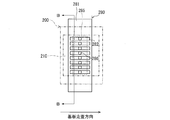
- FIG. 12 is a plan view of the deposition target substrate and the mask unit in the vacuum chamber in the vapor deposition apparatus of Patent Document 1, as viewed from the deposition target substrate side.
- 13 is a cross-sectional view schematically showing a schematic configuration of the main part of the vapor deposition apparatus of Patent Document 1, and is a cross-sectional view taken along the line BB in FIG.
- the vapor deposition apparatus 250 of Patent Document 1 includes a vacuum chamber 260, a mask unit 280, and a substrate moving mechanism (not shown).
- the mask unit 280 includes a shadow mask 281 and a vapor deposition source 285.
- the shadow mask 281 is provided with a plurality of openings 282.
- the vapor deposition source 285 individually accommodates the vapor deposition particles corresponding to each color, and has a plurality of injection ports 286 that eject the vapor deposition material as vapor deposition particles. .
- the deposition target substrate 200 is held such that the gap g1 between the deposition target substrate 200 and the shadow mask 281 is constant, and the deposition source 285 is fixed between the shadow mask 281 and the gap g2. Are arranged opposite to each other.
- the vapor deposition apparatus of Patent Document 1 moves the deposition target substrate 200 relative to the mask unit 280 as indicated by an arrow in FIG. 12, and thereby vapor deposition particles ejected from the ejection port 286 of the vapor deposition source 285.
- vapor deposition particles ejected from the ejection port 286 of the vapor deposition source 285. are sequentially deposited on the vapor deposition region 210 on the vapor deposition surface of the film formation substrate 200 through the opening 282 of the shadow mask 281, so that the vapor deposition film corresponding to the sub-pixels is formed on the vapor deposition region 210 of the film formation substrate 200.
- 211 patterns are formed.
- Vapor deposition particles are injected from each injection port so as to diffuse with a certain spread.
- the opening 282 has a certain width
- the shadow mask 281 and the TFT substrate 290 have a gap of g1
- the vapor deposition source 285 and the shadow mask 281 have a gap of g2. have.
- the vapor deposition particles emitted from the respective injection ports and passing through the opening 282 spread between the shadow mask 281 and the TFT substrate 290 and reach the TFT substrate 290. Therefore, the light emitting layer 291 formed on the TFT substrate 290 is not formed flat, but is formed so as to gradually spread over a range wider than the width of the opening 282.
- the red vapor deposition particles to be injected into the red sub-pixel reach the adjacent green sub-pixel, and the green vapor deposition particles and the red vapor deposition particles are mixed.
- the formation of one light emitting layer by vapor deposition particles having different colors is referred to as color mixing.
- the light emitting layer of the sub-pixel where the color mixture has occurred does not emit light of a desired wavelength or does not emit light, the display quality as a display device is degraded.
- FIG. 14 is a cross-sectional view illustrating one pixel of the organic light emitting display device manufactured by the thin film deposition apparatus of Patent Document 2.
- the organic light emitting display device of Patent Document 2 is connected to a drain electrode 357 of a thin film transistor TFT and is supplied with a positive power source 361 and a second electrode 363 that is provided so as to cover the entire pixel and supplies a negative power source. , And an organic layer 362 that is disposed between the first electrode 361 and the second electrode 363 and emits light.
- the organic layer 362 includes light emitting layers 362R, 362G, 362B and auxiliary layers 362R ', 362G'.
- the organic layer 362 has a green auxiliary layer 362G ′ and one end of the green light emitting layer 362G overlapped on one end of the blue light emitting layer 362B, and a red auxiliary layer 362R ′ and the other end of the green light emitting layer 362G.
- the red light emitting layer 362R is formed so that one end thereof is overlapped.
- the green auxiliary layer 362G ′ is interposed between the blue light emitting layer 362B and the green light emitting layer 362G, and the blue light emitting layer 362B and the green light emitting layer 362G adjacent to each other are not in direct contact with each other.
- the red auxiliary layer 362R ' is interposed between the green light emitting layer 362G and the red light emitting layer 362R, so that the green light emitting layer G and the red light emitting layer R adjacent to each other are not in direct contact with each other.
- Patent Document 2 describes that the light emission efficiency of the light emitting layer is greatly improved by the above configuration, the color mixing phenomenon disappears, and the color coordinate improvement effect is produced.
- the present invention has been made in view of the above-described problems, and an object of the present invention is to provide a display device and a display device manufacturing method in which a reduction in display quality due to color mixing of the light emitting layer is suppressed without reducing productivity. It is to provide.
- the region where the film thickness gradually increases in the cross-sectional shape of the light-emitting layer includes two regions. I found out.
- the two regions are a theoretical taper region (theoretical taper portion) in which the film thickness decreases in proportion to the distance from the center of the light emitting layer in plan view, based on the geometric structure of the vapor deposition apparatus, and the theoretical taper region. This is an actually measured taper region (actually tapered portion) where the film thickness decreases in a curved manner based on the distance from the center of the light emitting layer.
- this measured taper portion is formed to extend outward from the theoretical taper portion, when the film thickness is calculated based on the geometric structure of the vapor deposition apparatus and vapor deposition is performed, the actual taper portion of the light emitting layer is not the same. May reach the pixel. In this case, color mixing occurs.
- the inventors have observed the shape of the light emitting layer in the measured taper portion. If the position is 3 ⁇ m outside the boundary between the theoretical taper portion and the actually measured taper portion, the film thickness is sufficiently thin, so Even if it is formed in a wide range, the influence on the light emission characteristics of the light emitting layer is small, and it has been confirmed as a display device.
- the inventors have found a method for manufacturing a display device including a light emitting layer without degrading display quality in consideration of the verification result.
- a method for manufacturing a display device includes a substrate, and a plurality of pixel openings which are regions that emit light are adjacent to each other on the substrate.
- a non-display area which is an area between the matching pixel openings and does not emit light, is defined, and light of different colors is provided on the substrate corresponding to each pixel opening.
- the pixel A first light emitting layer is formed corresponding to a first pixel opening which is one of the mouths, and corresponds to a second pixel opening adjacent to the first pixel opening via the non-display area.
- the width of the mask opening is set to M.
- the width of the injection port is Wn
- the distance between the substrate and the deposition mask is G
- the distance between the substrate and the deposition source is Ts
- the width of the first pixel opening is
- the present invention it is possible to provide a display device and a method for manufacturing the display device, in which a reduction in display quality due to color mixing of the light emitting layer is suppressed without reducing productivity.
- FIG. 1 is a cross-sectional view showing a schematic configuration of an organic EL display device for RGB full-color display according to Embodiment 1 of the present invention. It is a top view which shows the structure of the pixel which comprises the organic electroluminescence display which concerns on Embodiment 1 of this invention.
- FIG. 3 is a cross-sectional view of the TFT substrate in the organic EL display device according to Embodiment 1 of the present invention, taken along line AA in FIG. It is a flowchart which shows the manufacturing process of an organic electroluminescence display in order of a process. It is sectional drawing of a TFT substrate and a vapor deposition apparatus for demonstrating the process of forming a light emitting layer in a TFT substrate using a vapor deposition apparatus.
- FIG. 1 is a cross-sectional view of a TFT substrate and a light emitting layer of the organic EL display device of Embodiment 1.
- FIG. 6 is a cross-sectional view of another example of the TFT substrate and the light emitting layer of the organic EL display device according to Embodiment 1.
- FIG. 6 is a cross-sectional view of a TFT substrate and a light emitting layer of an organic EL display device according to Embodiment 2.
- FIG. It is sectional drawing of the TFT substrate and light emitting layer of the organic electroluminescence display of Embodiment 3. It is the top view which looked at the film-forming substrate and mask unit in the vacuum chamber in the vapor deposition apparatus of patent document 1 as a prior art from the film-forming substrate side.
- It is sectional drawing which shows typically schematic structure of the principal part in the vapor deposition apparatus of patent document 1 as a prior art, and is BB arrow sectional drawing of FIG.
- a bottom emission type organic EL display device of RGB full color display that extracts light from the TFT substrate side will be described as an example.
- FIG. 1 is a cross-sectional view showing a schematic configuration of an organic EL display device for RGB full-color display according to the present embodiment.
- FIG. 2 is a plan view showing the configuration of the pixels constituting the organic EL display device shown in FIG. 1, and FIG. 3 shows the sub-pixels 2R, 2G, and 2B arranged in the organic EL display device shown in FIG.
- FIG. 3 is a cross-sectional view taken along line AA of the TFT substrate and the organic EL element when cut in the direction.
- the organic EL display device 1 of the present embodiment has a configuration in which an organic EL element 20, an adhesive layer 30, and a sealing substrate 40 are provided in this order on a TFT substrate 10. Yes.
- the organic EL element 20 includes a pair of substrates (TFT substrates) by bonding a TFT substrate 10 on which the organic EL element 20 is laminated to a sealing substrate 40 using an adhesive layer 30. 10 and the sealing substrate 40).
- TFT substrates substrates
- the organic EL element 20 is sealed between the TFT substrate 10 and the sealing substrate 40 in this way, so that oxygen or moisture can enter the organic EL element 20 from the outside. It is prevented.
- the TFT substrate 10 includes a TFT 12 (switching element), an interlayer film 13 (interlayer insulating film, planarizing film), a wiring 14, a first electrode 21, and an edge cover 15 on an insulating substrate 11. It has the structure formed in order.
- a plurality of wirings 14 including a plurality of gate lines laid in the horizontal direction and a plurality of signal lines laid in the vertical direction and intersecting the gate lines are provided on the insulating substrate 11, as shown in FIG. 2, a plurality of wirings 14 including a plurality of gate lines laid in the horizontal direction and a plurality of signal lines laid in the vertical direction and intersecting the gate lines are provided. It has been.
- a gate line driving circuit (not shown) for driving the gate line is connected to the gate line
- a signal line driving circuit (not shown) for driving the signal line is connected to the signal line.
- the organic EL display device 1 is a full-color active matrix organic EL display device.
- the regions surrounded by the wirings 14 have red (R), green (G), and blue (B), respectively.
- the sub-pixels 2R, 2G, and 2B that emit light of the respective colors are arranged in a matrix.
- one subpixel (dot) is defined corresponding to the intersection of these wirings 14, and R, G, and B light emitting areas are defined for each subpixel.
- the pixel 2 (that is, one pixel) has three sub-pixels 2R, 2G, and 2B: a red sub-pixel 2R that emits red light, a green sub-pixel 2G that emits green light, and a blue sub-pixel 2B that emits blue light. It is constituted by.
- pixel openings 16R, 16G, and 16B which are regions emitting light of each color, are defined corresponding to the sub-pixels 2R, 2G, and 2B.
- the pixel openings 16R, 16G, and 16B are provided with light-emitting layers 23R, 23G, and 23B that emit light of different colors and that emit light in the sub-pixels 2R, 2G, and 2B.
- the organic EL display device 1 including the red light emitting layer 23R, the green light emitting layer 23G, and the blue light emitting layer 23B as the light emitting layer will be described.
- the types of the light emitting layers are not limited to three, What is necessary is just to provide multiple types of light emitting layers.
- These light emitting layers 23R, 23G, and 23B are patterned by vapor deposition for each color of light to be emitted.
- the pixel openings 16R, 16G, and 16B will be described later.
- a first electrode 21 and a TFT 12 connected to the first electrode 21 are provided.
- the light emission intensity of each of the sub-pixels 2R, 2G, and 2B is determined by scanning and selection by the wiring 14 and the TFT 12.
- the organic EL display device 1 realizes image display by selectively causing the organic EL element 20 to emit light with desired luminance using the TFT 12.
- the interlayer film 13 is laminated on the insulating substrate 11 over the entire region of the insulating substrate 11 so as to cover the TFTs 12.
- the interlayer film 13 is provided with a contact hole 13 a for electrically connecting the first electrode 21 to the TFT 12.
- the first electrode 21 is a layer having a function of injecting (supplying) holes into an organic EL layer described later. As described above, the first electrode 21 is connected to the TFT 12 via the contact hole 13a.
- the edge cover 15 prevents the first electrode 21 and the second electrode 29 in the organic EL element 20 from being short-circuited when the organic EL layer becomes thin or the electric field concentration occurs at the pattern end of the first electrode 21. It is an insulating layer for preventing.
- the edge cover 15 is formed on the interlayer film 13 so as to cover the end of the first electrode 21.
- a portion of the first electrode 21 that is not covered by the edge cover 15 is a light emitting region that emits light.
- the portions where the first electrode 21 is provided on the TFT substrate 10 and the first electrode 21 is exposed without being covered by the edge cover 15 are the pixel openings 16R, 16G, and 16B.
- the region on the TFT substrate 10 where the edge cover 15 is provided is a non-display region 15R / 15G / 15B that does not emit light.
- the organic EL element 20 is a light emitting element that can emit light with high luminance by low-voltage direct current driving, and an organic EL layer and a second electrode 29 are laminated on the first electrode 21 in this order.
- the organic EL layer from the first electrode 21 side, the hole injection layer / hole transport layer 22, the light emitting layers 23R / 23G / 23B, the electron transport layer 27, and the electron injection layer 28 are arranged in this order. You may have the structure formed.
- the stacking order is that in which the first electrode 21 is an anode, the second electrode 29 is a cathode, the first electrode 21 is a cathode, and the second electrode 29 is an anode.
- the order of stacking is reversed.
- the hole injection layer / hole transport layer 22 is uniformly formed on the entire display region of the TFT substrate 10 so as to cover the first electrode 21 and the edge cover 15.
- light emitting layers 23R, 23G, and 23B are formed corresponding to the sub-pixels 2R, 2G, and 2B so as to cover the pixel openings 16R, 16G, and 16B, respectively. ing.
- the light emitting layers 23R, 23G, and 23B are layers having a function of emitting light by recombining holes injected from the first electrode 21 side and electrons injected from the second electrode 29 side. .
- the electron transport layer 27 is a layer having a function of increasing the electron transport efficiency from the second electrode 29 to the light emitting layers 23R, 23G, and 23B.
- the electron injection layer 28 is a layer having a function of increasing the electron injection efficiency from the second electrode 29 to the light emitting layers 23R, 23G, and 23B.
- the electron transport layer 27 is formed on the light emitting layer 23R / 23G / 23B and the hole injection layer / hole transport layer 22 so as to cover the light emitting layer 23R / 23G / 23B and the hole injection layer / hole transport layer 22.
- the TFT substrate 10 is formed uniformly over the entire display area.
- the electron injection layer 28 is uniformly formed on the electron transport layer 27 over the entire display region of the TFT substrate 10 so as to cover the electron transport layer 27.
- the second electrode 29 is a layer having a function of injecting electrons into the organic EL layer composed of the organic layers as described above.
- the second electrode 29 is uniformly formed on the electron injection layer 28 over the entire display region of the TFT substrate 10 so as to cover the electron injection layer 28.
- organic layers other than the light emitting layers 23R, 23G, and 23B are not essential layers as the organic EL layer, and may be appropriately formed according to the required characteristics of the organic EL element 20.
- a layer configuration as shown in the following (1) to (8) can be adopted.
- FIG. 4 is a flowchart showing the manufacturing steps of the organic EL display device in the order of steps.
- the manufacturing method of the organic EL display device 1 includes, for example, a TFT substrate manufacturing step (S1), a first electrode manufacturing step (S2), a hole injection layer and hole transport.
- the light emitting layers 23R, 2G, 2B corresponding to the subpixels 2R, 2G, 2B are formed on the hole injection layer / hole transport layer 22 so as to cover the pixel openings 16R, 16G, 16B.
- 23G and 23B are separately formed (pattern formation).
- the light emitting layers 23R, 23G, and 23B can be vapor-deposited on the TFT substrate 10 using a vapor deposition mask.
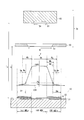
- FIG. 5 is a cross-sectional view of the TFT substrate and the vapor deposition apparatus for explaining a process of forming a light emitting layer on the TFT substrate using the vapor deposition apparatus.
- FIG. 5 is a diagram illustrating a process of forming the light emitting layer 23 ⁇ / b> R on the hole injection layer / hole transport layer 22.
- FIG. 5 is a diagram for mainly explaining the positional relationship between the vapor deposition apparatus and the TFT substrate in the light emitting layer vapor deposition process of the present embodiment, and the thickness and shape of the light emitting layer are simplified for explanation. It is shown.
- the vapor deposition apparatus 70 includes a vapor deposition source 60 and a vapor deposition mask 50, and is provided so that the vapor deposition mask 50 and the TFT substrate 10 face each other.
- the light emitting layers 23 ⁇ / b> R, 23 ⁇ / b> G, and 23 ⁇ / b> B of the organic EL display device 1 of the present embodiment are formed by depositing vapor deposition particles emitted from the vapor deposition source 60 on the TFT substrate 10.
- a vapor deposition mask 50 having a mask opening 51 is provided between the TFT substrate 10 and the vapor deposition source 60, and vapor deposition particles are vapor-deposited on the TFT substrate 10 through the mask opening 51.
- the vapor deposition source 60 has, for example, a mechanism for injecting vapor deposition particles upward.
- the vapor deposition source 60 has a plurality of vapor deposition source openings 61 (injection ports) for injecting (scattering) the vapor deposition material as vapor deposition particles on the surface facing the vapor deposition mask 50.
- the vapor deposition particles are ejected from the vapor deposition source opening 61 with a certain isotropic property.
- the width of the vapor deposition source opening 61 of the vapor deposition source 60 is Wn, and the width of the mask opening 51 of the vapor deposition mask 50 is M.
- the width M of the mask opening 51 is the width of the through hole provided in the vapor deposition mask 50 in plan view.
- the distance between the vapor deposition source 60 and the TFT substrate 10 is Ts, and the distance between the vapor deposition mask 50 and the TFT substrate 10 is G.
- deposition is performed with the center of the deposition source opening 61, the center of the mask opening 51, and the centers of the pixel openings 16R, 16G, and 16B arranged on the same straight line. Is preferred.
- the TFT substrate 10 is moved relative to the vapor deposition mask 50, and vapor deposition particles are sequentially deposited on the vapor deposition region on the vapor deposition surface of the TFT substrate 10 through the mask opening 51.
- vapor deposition particles are sequentially deposited on the vapor deposition region on the vapor deposition surface of the TFT substrate 10 through the mask opening 51.
- vapor deposition particles emitted from all positions of the vapor deposition source opening 61 on the TFT substrate 10 in plan view. are deposited (regions having a width of Wt in the drawing) and regions (depositions having a width of Wb in the drawing) where vapor deposition particles emitted from a part of the position of the deposition source opening 61 are deposited. is there.
- the vapor deposition particles are uniformly deposited. Therefore, the film of the light emitting layers 23R, 23G, and 23B in the region. The thickness is substantially uniform.
- portions having a uniform thickness and a flat cross-sectional shape are formed. This is referred to as a flat portion of the light emitting layers 23R, 23G, and 23B.
- the vapor deposition particles emitted from a part of the position of the vapor deposition source opening 61 on the TFT substrate 10 are vapor deposited, the vapor deposition particles are not uniformly deposited, and the light emitting layers 23R, 23G, The film thickness of the light emitting layers 23R, 23G, and 23B decreases according to the distance from the center of 23B.
- the portion where the film thickness changes according to the position on the TFT substrate 10 and the cross-sectional shape is not flat is referred to as a tapered portion of the light emitting layers 23R, 23G, and 23B.
- the tapered portions of the light emitting layers 23R, 23G, and 23B are formed so as to extend to the pixel openings 16R, 16G, and 16B of other adjacent subpixels 2R, 2G, and 2B, and thus one pixel opening 16R, 16G, and 16B.
- the light emitting layers 23R, 23G, and 23B that emit light of different colors that is, when color mixing occurs, light emission other than the desired color occurs or does not emit light.
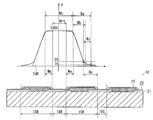
- FIG. 6 is a cross-sectional view of the light emitting layer formed on the TFT substrate by the light emitting layer vapor deposition process when cut in a direction perpendicular to the TFT substrate.
- the light emitting layer 23R is illustrated and described, but the same applies to the light emitting layers 23G and 23B.
- the distance G between the deposition mask 50 and the TFT substrate 10 From the distance Ts between the deposition source 60 and the TFT substrate 10, the distance G between the deposition mask 50 and the TFT substrate 10, the width Wn of the deposition source opening 61, and the width M of the mask opening 51, the light emitting layer 23R.
- the film thickness and shape of these are theoretically determined.
- the light-emitting layer 23R has a flat portion (hereinafter, a theoretical flat portion) that is a portion where the film thickness is constant, and a periphery of the theoretical flat portion, It includes a taper portion (hereinafter, theoretical taper portion) that is a portion where the film thickness decreases in proportion to the distance from the central axis y of the light emitting layer 23R.
- a theoretical flat portion that is a portion where the film thickness is constant
- a taper portion hereinafter, theoretical taper portion
- the shape of the light emitting layer 23 ⁇ / b> R actually formed on the TFT substrate 10 is different from the theoretically required shape, and it is not easy to actually measure, and its presence may not be specified.
- the inventors accurately measure the film thickness of the light emitting layers 23R, 23G, and 23B by using a high-precision step gauge, measuring means using TOF-SIMS (Time of Flight Secondary Ion Mass Spectroscopy), and a calibration sample. Succeeded.
- TOF-SIMS Time of Flight Secondary Ion Mass Spectroscopy
- TOF-SIMS IV manufactured by ION-TOF was used as TOF-SIMS.
- the solid line in FIG. 6 is the cross-sectional shape of the light emitting layer 23R obtained by actually measuring the film thickness.
- the light emitting layer 23R has a flat portion (hereinafter, measured flat portion) where the film thickness is constant, and the light emitting layer 23R.
- the taper portion (hereinafter, measured taper portion), which is a portion where the film thickness decreases according to the distance from the central axis y, includes a gentle R shape at the boundary between the measured flat portion and the measured taper portion. It was found that the width of the actually measured flat portion is smaller than the width of the theoretical flat portion in plan view.
- the actually measured taper portion has a film thickness that linearly decreases in accordance with the distance from the central axis y of the light emitting layer in plan view. It was found to include a linear taper portion (linear taper portion) and an actually measured curve taper portion (curve taper portion) which is outside the actually measured linear taper portion and whose film thickness decreases in a curved manner.
- the film thickness of the light emitting layer 23R in the actually measured linear taper portion is equivalent to the film thickness of the light emitting layer 23R in the theoretical taper portion, and can be calculated theoretically.
- the film thickness of the light emitting layer 23R in the theoretical flat part is 100%
- the film thickness of the light emitting layer 23R at the boundary between the actually measured linear taper part and the actually measured curve taper part is It was found to be 2% (become 1/50 of the thickness of the light emitting layer 23R in the theoretical flat portion).
- the width Wu of the peripheral region in plan view is It was found to be 3 to 5 ⁇ m (3 ⁇ m ⁇ Wu ⁇ 5 ⁇ m). And it turned out that a peripheral region is formed even to the outer side of a theoretical taper part.
- ⁇ Light emitting layer> Based on the shape of the light emitting layer 23R, a preferable method for forming the light emitting layer 23R of the present embodiment will be described in detail from the viewpoint of color mixture in adjacent subpixels and light emission characteristics in the own subpixel.
- Such deterioration in display quality is caused by color mixing in the pixel opening 16R of the sub-pixel 2R.
- display quality does not deteriorate even if color mixing occurs.
- the inventors have mixed the light emitting layers 23R of other colors into the pixel openings 16G and 16B. It has been found that even if color mixing occurs, if the film thickness of the light emitting layer 23R of the other color is 1% or less of the film thickness of the light emitting layers 23G and 23B, the light emission characteristics are not greatly affected.
- FIG. 7 is a cross-sectional view of the TFT substrate and the light emitting layer of the organic EL display device of this embodiment when the light emitting layer is formed on the TFT substrate by the light emitting layer vapor deposition process.
- FIG. 7 corresponds to a cross-sectional view taken along the line AA in FIG.
- the detailed configuration of the TFT substrate 10 is omitted.
- the TFT substrate 10 and the light emitting layer 23R formed on the TFT substrate 10 are illustrated separately.
- the light emitting layers 23R, 23G, and 23B having the same film thickness are formed in the pixel openings 16R, 16G, and 16B of the sub-pixels 2R, 2G, and 2B, the light emission of the organic EL display device 1 of the present embodiment is performed.
- the film thicknesses of the layers 23R, 23G, and 23B are controlled as follows.
- the measured linear taper portion and the measured curve taper portion of the light emitting layer 23R formed corresponding to the pixel opening portion 16R (first pixel opening portion).
- the shortest distance between the boundary (first boundary) and the pixel opening 16G (second pixel opening) of the sub-pixel 2G adjacent to the sub-pixel 2R is 3 ⁇ m or more, more preferably 5 ⁇ m. That's it.
- the width Wu of the peripheral region is 3 to 5 ⁇ m (3 ⁇ m ⁇ Wu ⁇ 5 ⁇ m) in plan view.
- the portion of the light emitting layer 23R formed in the pixel opening 16G is outside the peripheral region, and the thickness thereof is 1% or less of the thickness of the light emitting layer 23R in the theoretical flat portion.
- the film thickness of the light emitting layer 23G is equal to the film thickness of the light emitting layer 23R
- the film thickness of the part formed in the pixel opening 16G in the light emitting layer 23R is the thickness of the light emitting layer 23G in the theoretical flat part. It can be said that it is 1% or less of the film thickness.
- the thickness of the light emitting layer 23R formed in the pixel opening 16G is 1% or less of the film thickness in the flat portion of the light emitting layer 23G (second light emitting layer, not shown), the light emitting layer 23G of the pixel opening 16G. Normally emits green light and does not affect the light emission characteristics of the pixel opening 16G.
- the light emission characteristics of the light emitting layer 23R greatly depend on the film thickness.
- the film thickness of the light emitting layer 23R in the pixel opening 16R is preferably uniform.
- the light emitting layer 23R when the light emitting layer 23R is formed on the TFT substrate 10, it is preferable to form the light emitting layer 23R so that the pixel opening 16R is covered with the theoretical flat portion of the light emitting layer 23R.
- the light emitting layer 23R is formed in the pixel opening portion 16R on the TFT substrate 10 so that the boundary portion between the theoretical flat portion and the theoretical taper portion overlaps the end portion of the pixel opening portion 16R in plan view.
- the film thickness of the light emitting layer 23R in the pixel opening 16R becomes substantially constant, the light emission characteristics in the sub-pixel 2R become substantially uniform.
- the formation of the light emitting layer 23R in consideration of the color mixture in the adjacent subpixels and the light emission characteristics in the own subpixel prevents the display quality from being deteriorated due to the color mixture in the pixel openings 16G and 16B, and Thus, uniform light emission characteristics can be obtained in the sub-pixel 2R.
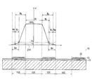
- FIG. 8 is a cross-sectional view of the TFT substrate, the light emitting layer, and the vapor deposition apparatus for explaining the light emitting layer vapor deposition step of the present embodiment.
- the TFT substrate 10 and the light emitting layer 23R in FIG. 8 correspond to the cross-sectional view taken along the line AA in FIG.
- the TFT substrate is arranged so that the center of the pixel opening, the center of the mask opening 51, and the center of the deposition source opening 61 are arranged in a straight line. 10, the vapor deposition mask 50, and the vapor deposition source 60 are aligned.
- the width of the pixel openings 16R, 16G, and 16B (the width of the exposed portion of the first electrode 21) is P
- the width of the non-display areas 15R, 15G, and 15B (the width of the edge cover 15) is Lc.
- the width of the pixel opening for the thickness of the portion of the light emitting layer 23R formed in the pixel openings 16G and 16B to be 1% or less of the film thickness in the flat portion of the light emitting layer 23R.
- the size of P and the width Lc of the non-display area needs to be within the following range.
- the width Wg is a width in a plan view of a tapered region of the light emitting layer and having a film thickness of 1 ⁇ m or more.
- the width Wg is expressed by the following equation. expressed.
- the triangle whose bottom width is Wb and whose measured taper portion of the light emitting layer is a hypotenuse and the triangle whose base width is Wb ′ and whose measured taper portion of the light emitting layer is a hypotenuse are: They are similar triangles.
- the ratio of Wb and Wb ′ can be obtained as follows.
- Wg is expressed as follows using the width Wb of the theoretical taper portion and the peripheral region Wu.
- the width P of the pixel opening, the width Lc of the non-display area, the width M of the mask opening 51, the distance Ts between the vapor deposition source 60 and the TFT substrate 10, the vapor deposition mask 50 and the TFT substrate 10 And the width Wn of the vapor deposition source opening 61 are design parameters in the light emitting layer vapor deposition step, and can be controlled by changing the vapor deposition conditions. On the other hand, it is difficult to control the width of the peripheral region Wu by changing the deposition conditions.
- the peripheral region is formed to extend outward from the theoretical taper portion.
- the vapor deposition method of this embodiment is characterized in that the vapor deposition apparatus 70 and the TFT substrate 10 are designed in consideration of the formation of the peripheral region.
- the deposition conditions are determined so that P, Lc, M, Ts, G, and Wn satisfy the following formula.
- the width Wu of the peripheral region is 3 ⁇ m ⁇ Wu ⁇ 5 ⁇ m Because 3 ⁇ m ⁇ Dm (5) If it is, it can suppress that the light emitting layer of a peripheral region reaches the pixel opening part of an adjacent pixel, and can suppress the fall of the display quality by color mixing. Also, 5 ⁇ m ⁇ Dm Expression (6) If so, it is possible to more reliably suppress the light emitting layer in the peripheral region from reaching the pixel opening of the adjacent pixel, and to suppress the deterioration in display quality due to color mixing.
- the design margin Dm is Dm ⁇ Wu + Wm It is preferable that
- the design margin Dm is 3 ⁇ m + Wm ⁇ Dm (7) Or 5 ⁇ m + Wm ⁇ Dm (8) It is preferable that
- design margin Dm in consideration of 5 to 20 ⁇ m as the deposition margin Wm.
- vapor deposition is performed so as to satisfy the relationship of the above formulas (4) and formulas (5) to (8).
- the light emitting layer can be produced without causing deterioration in display quality due to color mixing. 23R can be formed.
- the light emitting layer 23R can be formed without causing deterioration in display quality due to color mixing.
- the width M of the mask opening, the width Wn of the injection port, the distance G between the substrate and the vapor deposition mask, and the distance Ts between the substrate and the vapor deposition source can be set.
- the vapor deposition conditions may be determined so as to satisfy the expressions (9) and (7). That is, [P + 2Lc ⁇ M ⁇ ⁇ (0.96 ⁇ G ⁇ Wn) / Ts ⁇ ⁇ Wm] / 2 ⁇ 3 ⁇ m It becomes.
- the pixel opening 16R is preferably covered with the theoretical flat portion of the light-emitting layer 23R.
- the width P of the pixel openings 16R, 16G, and 16B for forming the light emitting layer 23R so that the pixel opening 16R is covered with the theoretical flat portion of the light emitting layer 23R is expressed as follows.
- P P ⁇ Wt That is, P ⁇ ⁇ (Ts ⁇ M) ⁇ (G ⁇ Wn) / (Ts ⁇ G) ⁇ (10)
- the arrangement of the vapor deposition source 60, the vapor deposition mask 50, and the TFT substrate 10 and the mask so as to satisfy the above formula (11) By designing the width M of the opening 51 and the width Wn of the vapor deposition source opening 61, the light emitting layer 23R is formed so that uniform light emission characteristics can be obtained in the sub-pixel 2R while maximizing the aperture ratio. be able to.
- FIG. 9 is a cross-sectional view of another example of the TFT substrate and the light emitting layer of the present embodiment when the light emitting layer is formed on the TFT substrate by the light emitting layer vapor deposition step.
- FIG. 9 corresponds to a cross-sectional view taken along the line AA in FIG.
- the boundary portion between the measured flat portion and the measured tapered portion has a gentle R shape, and the width of the measured flat portion in plan view. Wrt is narrower than the width Wt of the theoretical flat portion, and the actually measured flat portion is inside the theoretical flat portion.
- FIG. A margin indicated by a width Wm may be included in the design of the light emitting layer.
- the portion of the theoretical flat portion having the width Wm from the outside is formed so as to overlap the non-display region in plan view.
- the light emitting layer 24R can be formed so that the pixel opening 16R and the measured flat portion of the light emitting layer 23R overlap in plan view, and the film thickness of the light emitting layer 24R in the pixel opening 16R is made more uniform. be able to.
- ⁇ Vapor deposition design> The design of the vapor deposition device 70 and the pixel openings 16R, 16G, and 16B for forming the light emitting layers 24R, 24G, and 24B of other examples as shown in FIG. 9 will be described.
- the width P of the pixel openings 16R, 16G, and 16B for forming the light emitting layer 24R so that the pixel opening 16R is covered with the measured flat portion of the light emitting layer 24R is expressed as follows.
- a light emitting layer vapor deposition step of forming a light emitting layer on a TFT substrate having a pixel opening of width P the arrangement of the vapor deposition source 60, the vapor deposition mask 50, and the TFT substrate 10 and the mask so as to satisfy the above formula (14)
- the width M of the opening 51 and the width Wn of the vapor deposition source opening 61 the light emitting layer 23R is formed so that more uniform light emission characteristics can be obtained in the sub-pixel 2R while maximizing the aperture ratio. can do.
- Equation (1) when considering the deposition margin Wm, P + 2Lc ⁇ Wt + 2Wg + 2Wm (15) It becomes.
- P + 2Lc Wt + 2Wg + 2Wm Formula (17) It is expressed.
- the deposition conditions may be determined so that P, Lc, M, Ts, G, and Wn satisfy the following formula (20).
- FIG. 10 is a cross-sectional view of the TFT substrate and the light emitting layer of this embodiment when the light emitting layer is formed on the TFT substrate by the light emitting layer vapor deposition step.
- FIG. 10 corresponds to a cross-sectional view taken along the line AA in FIG.
- the light emitting layer of the organic EL display device of the present embodiment is controlled as follows.
- a first boundary portion (not shown) that is a boundary portion between the actually measured linear taper portion and the actually measured curve taper portion of the light emitting layer 24R, and the pixel opening portion 16G of the sub pixel 2G adjacent to the sub pixel 2R.
- the shortest distance between is 3 ⁇ m to 5 ⁇ m or 3 ⁇ m + Wm to 5 ⁇ m + Wm.
- the portion of the light emitting layer 24R formed in the pixel opening 16G is outside the peripheral region, and the film thickness thereof is that of the light emitting layer 24G in the flat portion. Since it is 1% or less of the film thickness, green light is normally emitted from the pixel opening 16G without affecting the light emission characteristics of the pixel opening 16G.
- the organic EL display device 1 of the first embodiment when the theoretical flat portion has a thickness of 100%, the position where the thickness of the light emitting layer 24R is 1% and the subpixel adjacent to the subpixel 2R. The end of the 2G pixel opening 16G overlaps in plan view. Therefore, the ratio of the non-display regions 15R, 15G, and 15B occupying the area of the TFT substrate 10 can be reduced, and the aperture ratio of the organic EL display device can be improved.
- ⁇ Vapor deposition design> The design of the vapor deposition device 70 and the pixel openings 16R, 16G, and 16B for forming the light emitting layer 25R in the light emitting layer vapor deposition step that is a part of the manufacturing process of the organic EL display device of the present embodiment will be described.
- the width P of the pixel opening, the width Lc of the non-display area, the width M of the mask opening 51, and the distance Ts between the vapor deposition source 60 and the TFT substrate 10 In equation (4) showing the relationship between the distance G between the vapor deposition mask 50 and the TFT substrate 10, the width Wn of the vapor deposition source opening 61, and the design margin Dm, 3 ⁇ m ⁇ Dm ⁇ 5 ⁇ m Formula (21) Vapor deposition conditions are determined so as to satisfy the above.
- the light emitting layer 25R can be formed without causing deterioration in display quality due to color mixing.
- the design margin Dm is 3 ⁇ m + Wm ⁇ Dm ⁇ 5 ⁇ m + Wm (22) It is preferable to design as follows.
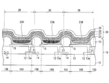
- FIG. 11 is a cross-sectional view of the TFT substrate and the light emitting layer of this embodiment when the light emitting layer is formed on the TFT substrate by the light emitting layer vapor deposition step.
- FIG. 11 corresponds to a cross-sectional view taken along the line AA in FIG.
- the light emitting layer is formed so that the pixel opening 16R of the TFT substrate 10 is covered with the theoretical flat portion or the measured flat portion of the light emitting layer.
- the pixel opening 16R of the TFT substrate 10 has a film thickness of 90% or more when the film thickness of the theoretical flat portion of the light emitting layer 26R is 100%. Covered by part. In other words, if the thickness of the theoretical flat portion of the light emitting layer 26R is 1, the thickness of the light emitting layer 26R at the end of the pixel opening 16R is 9/10 or more and less than 1.
- the maximum value of the thickness of the light emitting layer in the pixel opening is set to 100%, in many cases, if the thickness of the light emitting layer formed in the pixel opening is 90% or more, the light emission characteristics in the sub-pixel are obtained. There is often no difference.
- the light emitting layer 26R is formed so that the pixel opening 16R is covered with a region where the film thickness of the light emitting layer 26R is 90% or more.
- the width Wt ′ of the region where the film thickness of the light emitting layer 26R is 90% or more is expressed by the following formula and is larger than the width Wt of the theoretical flat portion.
- Wt ′ Wt + 2 ⁇ 0.1 ⁇ Wb Therefore, by increasing the width of the pixel opening 16R to Wt ′, the ratio of the pixel openings 16R, 16G, and 16B on the TFT substrate 10 can be increased, and the aperture ratio can be further increased.
- ⁇ Vapor deposition design> The design of the vapor deposition device 70 and the pixel openings 16R, 16G, and 16B for forming the light emitting layer 26R in the light emitting layer vapor deposition step that is a part of the manufacturing process of the organic EL display device of the present embodiment will be described.
- the width P of the pixel openings 16R, 16G, and 16B for forming the light emitting layer 2R so that the pixel opening 16R is covered with a portion of the light emitting layer 26R that is 90% or more of the film thickness is expressed as follows. Is done.
- the light emitting layers 26R, 26G, and 16B can be formed so that the pixel openings 16R, 16G, and 16B are covered with the regions where the film thickness of the light emitting layers 26R, 26G, and 26B is 90% or more.
- the arrangement of the vapor deposition source 60, the vapor deposition mask 50, and the TFT substrate 10 and the mask so as to satisfy the above formula (25) By designing the width M of the opening 51 and the width Wn of the vapor deposition source opening 61, the light emitting layer 26R is formed so as to maximize the aperture ratio while ensuring uniform light emission characteristics in the sub-pixel 2R. Can do.
- a manufacturing method of a display device includes a substrate (TFT substrate 10), and a plurality of pixel openings which are light emitting regions on the substrate and the pixel openings adjacent to each other.
- a non-display area which is an area between the areas and is an area that does not emit light, is defined, and a plurality of types that emit light of different colors on the substrate in correspondence with the pixel openings.
- a light emitting layer is formed on the substrate, a vapor deposition mask (50) having a mask opening (51), and an injection port (vapor deposition source opening 61) for injecting vapor deposition particles.
- a first light emitting layer is formed corresponding to a first pixel opening which is one of the pixel openings, and is adjacent to the first pixel opening through the non-display area.
- the width of the mask opening is M
- the width of the injection port is Wn
- the distance between the substrate and the vapor deposition mask is G
- the distance between the substrate and the vapor deposition source is Ts
- the width of the first pixel opening is P and the width of the non-display area is Lc
- P + 2Lc ⁇ ⁇ (Ts ⁇ M + 0.96 ⁇ G ⁇ Wn) / (Ts ⁇ G) ⁇ + 2Dm, 3 ⁇ m ⁇ Dm ⁇ 5 ⁇ m is satisfied.
- the first light emitting layer formed in the first pixel opening on the TFT substrate is formed flat in the conventional method. Instead, it is formed so as to gradually widen over a range wider than the width of the first pixel opening. As a result, it may be formed over the second pixel opening, and color mixing may occur in the second pixel opening.
- the light emitting layer deposition process is designed in consideration of the thickness of the light emitting layer in a region where the light emitting layer gradually decreases.
- the method for manufacturing a display device is the above-described aspect 1 or 2, in which the center of the pixel opening, the center of the mask opening, and the center of the emission port are straight in plan view.
- the substrate, the vapor deposition mask, and the vapor deposition source are aligned so as to be arranged on a line, and in the direction in which the first pixel opening and the second pixel opening are aligned, P ⁇ ⁇ ( Ts ⁇ M) ⁇ (G ⁇ Wn) ⁇ / (Ts ⁇ G) may be satisfied.
- the thickness of the first light emitting layer formed in the first pixel opening can be made uniform. Thereby, the light emission characteristics of the first light emitting layer in the first pixel opening can be made uniform.
- the method for manufacturing a display device is the above-described aspect 1 or 2, in which the center of the pixel opening, the center of the mask opening, and the center of the emission port are straight when viewed in plan.
- the substrate, the vapor deposition mask, and the vapor deposition source are aligned so as to be arranged on a line, and in the direction in which the first pixel opening and the second pixel opening are aligned, ⁇ (Ts ⁇ M) ⁇ (G ⁇ Wn) / (Ts ⁇ G) ⁇ ⁇ P ⁇ ⁇ (Ts ⁇ M) ⁇ (0.8 ⁇ G ⁇ Wn) ⁇ / (Ts ⁇ G) may be satisfied.
- the first light emitting layer is formed so that the thickness of the first light emitting layer formed in the first pixel opening is 90% or more and 100% or less of the film thickness of the thickest part. can do.
- the first light emitting layer is formed in this way, the light emission characteristics of the first light emitting layer in the first pixel opening do not excessively deteriorate the display quality.
- the first pixel opening can be maximized within the range in which the display quality is not excessively lowered by the above process. Thereby, the aperture ratio of the display device can be increased.
- the center of the pixel opening, the center of the mask opening, and the center of the emission port are aligned in a plan view.
- a method for manufacturing a display device provides the method for manufacturing a display device according to any one of the above aspects 1 to 5, wherein the width is P in the direction in which the first pixel opening and the second pixel opening are aligned.
- One pixel opening and the non-display area having a width Lc are defined on the substrate, and in the light emitting layer deposition step, P + 2Lc ⁇ ⁇ (Ts ⁇ M + 0.96 ⁇ G ⁇ Wn) / ( Ts-G) ⁇ + 2Wu And 3 ⁇ m ⁇ Wu ⁇ 5 ⁇ m, the width M of the mask opening, the width Wn of the injection port, the distance G between the substrate and the vapor deposition mask, the substrate and the above A distance Ts between the deposition source and the deposition source may be set, and the deposition particles may be deposited on the substrate.
- the width M of the mask opening, the width Wn of the injection port, the substrate, and the vapor deposition mask are prevented so as to prevent the display quality from being deteriorated due to the first light emitting layer being mixed in the second pixel opening.
- the distance Ts between the substrate and the deposition source can be set, and the deposited particles can be deposited on the substrate.
- the present invention can be used for an organic EL display device having a light emitting layer in each sub-pixel.
- Organic EL display device 10 TFT substrate (substrate) 15R / 15G / 15B Non-display area 16R / 16G / 16B Pixel opening 23R / 23G / 23B Light emitting layer 24R / 24G / 24B Light emitting layer 25R / 25G / 25B Light emitting layer 26R / 26G / 26B Light emitting layer 50 Evaporation mask 51 Mask opening Part 60 Deposition source 61 Deposition source opening (injection port)
Landscapes
- Chemical & Material Sciences (AREA)
- Engineering & Computer Science (AREA)
- Chemical Kinetics & Catalysis (AREA)
- Materials Engineering (AREA)
- Mechanical Engineering (AREA)
- Metallurgy (AREA)
- Organic Chemistry (AREA)
- Manufacturing & Machinery (AREA)
- Electroluminescent Light Sources (AREA)
- Devices For Indicating Variable Information By Combining Individual Elements (AREA)
- Physical Vapour Deposition (AREA)
Abstract
発光層の混色を生じることによる表示品位の低下を抑制した表示装置を提供する。基板(10)に蒸着粒子を蒸着させるときに、マスク開口部(51)の幅をM、射出口(61)の幅をWn、TFT基板(10)と蒸着マスク(50)との間の距離をG、TFT基板(10)と蒸着源(60)との間の距離をTs、第1画素開口部の幅をP、非表示領域の幅をLcとすると、P+2Lc≧{(Ts×M+0.96×G×Wn)/(Ts-G)}+2Dmと、3μm≦Dm≦5μmと、を満足する。
Description
本発明は表示装置の製造方法に関する。
フルカラーの有機EL(Electro luminescence)表示装置は、一般的に、赤(R)、緑(G)、青(B)の各色の有機EL素子をサブ画素として基板上に配列形成してなり、TFTを用いて、これら有機EL素子を選択的に所望の輝度で発光させることにより画像表示を行う。
このような有機EL表示装置の製造においては、各色に発光する有機発光材料からなる発光層が、発光素子である有機EL素子毎にパターン形成される。発光層のパターン形成を行う方法としては、例えば、シャドウマスクと称される蒸着用のマスクを用いた蒸着法が知られている。
特許文献1には、シャドウマスクを用いた蒸着装置および蒸着方法について記載されている。図12は、特許文献1の蒸着装置における真空チャンバ内の被成膜基板とマスクユニットとを被成膜基板側から見た平面図である。図13は、特許文献1の蒸着装置における要部の概略構成を模式的に示す断面図であり、図12のB-B矢視断面図である。
図12および13に示すように、特許文献1の蒸着装置250は、真空チャンバ260と、マスクユニット280と、図示しない基板移動機構とを備えている。マスクユニット280は、図12に示すように、シャドウマスク281と、蒸着源285とを備えている。
シャドウマスク281には、複数の開口部282が設けられている。蒸着源285は、各色に発光する発光層を形成するために、上記各色に対応した蒸着粒子を個別に収容しており、蒸着材料を蒸着粒子として射出させる複数の射出口286を有している。
図13に示すように、被成膜基板200は、シャドウマスク281との間の隙間g1が一定となるように保持されており、蒸着源285は、シャドウマスク281との間に一定の隙間g2を有して対向配置されている。
特許文献1の蒸着装置は、図12中に矢印で示すように、被成膜基板200をマスクユニット280に対して相対移動させ、これにより、蒸着源285の射出口286から射出させた蒸着粒子を、シャドウマスク281の開口部282を介して被成膜基板200の蒸着面における蒸着領域210に順次蒸着させることで、被成膜基板200の蒸着領域210に、サブ画素に対応して蒸着膜211のパターンを成膜するものである。
蒸着粒子は、各射出口から一定の広がりを持って拡散するように射出される。図13に示すように、開口部282は一定の幅を有しており、シャドウマスク281とTFT基板290とはg1の間隔を有しており、蒸着源285とシャドウマスク281とはg2の間隔を有している。
そのため、各射出口から射出され開口部282を通過した蒸着粒子は、シャドウマスク281とTFT基板290との間において広がり、TFT基板290に到達する。そのため、TFT基板290上に形成される発光層291は、平坦には形成されず、開口部282の幅より広い範囲に及び、漸減的に広がるように形成される。
そのため、例えば、赤のサブ画素内に射出されるべき赤色蒸着粒子が、隣の緑のサブ画素内に及んでしまい、緑色蒸着粒子と赤色蒸着粒子とが混ざることとなる。以下、異なる複数の色の蒸着粒子により1つの発光層が形成されることを、混色という。
混色を生じたサブ画素の発光層からは、所望の波長の光が出射されなかったり、発光しなかったりという不具合を生じるため、表示装置としての表示品位が低下する。
図14は、特許文献2の薄膜蒸着装置により製造された有機発光ディスプレイ装置のうち、一画素を図示した断面図である。
特許文献2の有機発光ディスプレイ装置は、薄膜トランジスタTFTのドレイン電極357に連結され、プラス電源を供給される第1電極361と、全体画素を覆うように備えられてマイナス電源を供給する第2電極363、及びこれら第1電極361と第2電極363との間に配されて発光する有機層362とを備えている。有機層362は、発光層362R、362G、362Bと補助層362R’、362G’とを備えている。
そして、有機層362は、青色発光層362Bの一端部上に緑色補助層362G’及び緑色発光層362Gの一端部がオーバーラップされ、緑色発光層362Gの他端部上に赤色補助層362R’及び赤色発光層362Rの一端部がオーバーラップされるように形成される。
これにより、青色発光層362Bと緑色発光層362Gとの間に緑色補助層362G’が介在され、互いに隣接した青色発光層362Bと緑色発光層362Gとが直接接触しなくなる。また、緑色発光層362Gと赤色発光層362Rとの間に赤色補助層362R’が介在され、互いに隣接した緑色発光層Gと赤色発光層Rとが直接接触しなくなる。
特許文献2には、上記の構成により発光層の発光効率が大きく向上し、混色現象が消え、色座標改善効果が生じることが記載されている。
しかしながら、特許文献2の有機発光ディスプレイ装置のように、各色間に補助層を挿入する場合、有機層の形成工程の工数が増大し、生産性が著しく低下するという問題がある。
本発明は、上記の問題点に鑑みなされたものであって、その目的は、生産性を低下させることなく、発光層の混色による表示品位の低下を抑制した表示装置及び表示装置の製造方法を提供することにある。
発明者らは、マスクを用いた蒸着により形成された発光層の形状について検証を行った結果、発光層の断面形状において、膜厚が漸減的に広がる領域には、2つの領域が含まれていることを見出した。2つの領域とは、蒸着装置の幾何学的構造に基づいて、平面視における発光層の中心からの距離に比例して膜厚が小さくなる理論テーパ領域(理論テーパ部)と、上記理論テーパ領域の外側にあり、発光層の中心からの距離に基づいて曲線的に膜厚が小さくなる実測テーパ領域(実測テーパ部)である。
この実測テーパ部は、理論テーパ部よりも外側に広がって形成されるため、蒸着装置の幾何学的構造に基づいて膜厚を算出し、蒸着を行った場合、発光層の実測テーパ部が他の画素にまで及んでしまうことがある。この場合、混色を生じてしまう。
発明者らは、実測テーパ部における発光層の形状を観察したところ、理論テーパ部と実測テーパ部との境界部から3μm外側の位置であれば、膜厚が十分に薄いため、隣の画素に及んで形成されたとしても発光層の発光特性に与える影響は小さく、表示装置としてのことを確認した。
発明者らは、上記の検証結果を考慮して、表示品位を低下させることなく、発光層を備える表示装置を製造する方法を見出した。
上記の課題を解決するために、本発明の一態様に係る表示装置の製造方法は、基板を有しており、上記基板上に、光を発する領域である複数の画素開口部と、互いに隣り合う上記画素開口部の間の領域であり、光を発しない領域である非表示領域とが規定されており、上記基板上に、上記各画素開口部に対応して、互いに異なる色の光を発する複数種の発光層が形成されている表示装置の製造方法であって、上記基板と、マスク開口部を有する蒸着マスクと、蒸着粒子を射出する射出口を有する蒸着源とをこの順に配置し、上記基板に、上記マスク開口部を介して上記蒸着粒子を蒸着させることで、上記基板上の上記画素開口部に対応する位置に上記発光層を形成する発光層蒸着工程を含んでおり、上記発光層蒸着工程において、上記画素開口部のうちの一つである第1画素開口部に対応して第1発光層を形成し、上記非表示領域を介して上記第1画素開口部に隣接する第2画素開口部に対応して、上記第1発光層が発する光の色とは異なる色の光を発する第2発光層を形成するように、上記基板に上記蒸着粒子を蒸着させるときに、上記マスク開口部の幅をMとし、上記射出口の幅をWnとし、上記基板と上記蒸着マスクとの間の距離をGとし、上記基板と上記蒸着源との間の距離をTsとし、上記第1画素開口部の幅をPとし、上記非表示領域の幅をLcとすると、P+2Lc≧{(Ts×M+0.96×G×Wn)/(Ts-G)}+2Dmと、3μm≦Dm≦5μmと、を満足することを特徴とする。
本発明の一態様によれば、生産性を低下させることなく、発光層の混色による表示品位の低下を抑制した表示装置及び表示装置の製造方法を提供することができる。
〔実施形態1〕
以下、本発明の実施の一形態について、図1~図9に基づいて詳細に説明する。
以下、本発明の実施の一形態について、図1~図9に基づいて詳細に説明する。
本実施の形態では、本実施の形態に係る表示装置の一例として、TFT基板側から光を取り出すボトムエミッション型でRGBフルカラー表示の有機EL表示装置を例に挙げて説明する。
<表示装置の構成>
まず、上記有機EL表示装置1の全体構成について以下に説明する。
まず、上記有機EL表示装置1の全体構成について以下に説明する。
図1は、本実施形態のRGBフルカラー表示の有機EL表示装置の概略構成を示す断面図である。また、図2は、図1に示す有機EL表示装置を構成する画素の構成を示す平面図であり、図3は、図2に示す有機EL表示装置において、サブ画素2R・2G・2Bが並ぶ方向に切断した場合のTFT基板および有機EL素子のA-A線矢視断面図である。
図1に示すように、本実施の形態の有機EL表示装置1は、TFT基板10上に、有機EL素子20、接着層30、封止基板40が、この順に設けられた構成を有している。
図1に示すように、有機EL素子20は、該有機EL素子20が積層されたTFT基板10を、接着層30を用いて封止基板40と貼り合わせることで、これら一対の基板(TFT基板10、封止基板40)間に封入されている。
上記有機EL表示装置1は、このように有機EL素子20がTFT基板10と封止基板40との間に封入されていることで、有機EL素子20への酸素や水分の外部からの浸入が防止されている。
図3に示すように、TFT基板10は、絶縁基板11上に、TFT12(スイッチング素子)、層間膜13(層間絶縁膜、平坦化膜)、配線14、第1電極21、エッジカバー15がこの順に形成された構成を有している。
絶縁基板11上には、図2に示すように、水平方向に敷設された複数のゲート線と、垂直方向に敷設され、ゲート線と交差する複数の信号線とからなる複数の配線14が設けられている。ゲート線には、ゲート線を駆動する図示しないゲート線駆動回路が接続され、信号線には、信号線を駆動する図示しない信号線駆動回路が接続されている。
有機EL表示装置1は、フルカラーのアクティブマトリクス型の有機EL表示装置であり、平面視において、これら配線14で囲まれた領域に、それぞれ、赤(R)、緑(G)、青(B)の各色の光を発するサブ画素2R・2G・2Bが、マトリクス状に配列されている。
すなわち、これら配線14の交点に対応して、1つのサブ画素(ドット)が規定されており、サブ画素毎にR、G、Bの発光領域が規定されている。
画素2(すなわち、1画素)は、赤色の光を発する赤色サブ画素2R、緑色の光を発する緑色サブ画素2G、青色の光を発する青色サブ画素2Bの、3つのサブ画素2R・2G・2Bによって構成されている。
TFT基板10上には、各サブ画素2R・2G・2Bに対応して、各色の光を発する領域である画素開口部16R・16G・16Bが規定されている。画素開口部16R・16G・16Bには、各サブ画素2R・2G・2Bにおける発光を担う、互いに異なる色の光を発する発光層23R・23G・23Bが設けられている。
以下の説明では、発光層として、赤色発光層23Rと、緑色発光層23Gと、青色発光層23Bとを備える有機EL表示装置1について説明するが、発光層の種類は3つに限定されず、複数種の発光層を備えていればよい。
これら発光層23R・23G・23Bは、発光する光の色毎に、蒸着によりパターン形成されている。なお、画素開口部16R・16G・16Bについては後述する。
各サブ画素2R・2G・2Bに対応して、第1電極21と、第1電極21に接続されたTFT12とが設けられている。各サブ画素2R・2G・2Bの発光強度は、配線14およびTFT12による走査および選択により決定される。このように、有機EL表示装置1は、TFT12を用いて、有機EL素子20を選択的に所望の輝度で発光させることにより画像表示を実現している。
層間膜13は、各TFT12を覆うように、上記絶縁基板11上に、上記絶縁基板11の全領域に渡って積層されている。
また、層間膜13には、第1電極21をTFT12に電気的に接続するためのコンタクトホール13aが設けられている。
第1電極21は、後述する有機EL層に正孔を注入(供給)する機能を有する層である。第1電極21は、前記したようにコンタクトホール13aを介してTFT12と接続されている。
エッジカバー15は、第1電極21のパターン端部で有機EL層が薄くなったり電界集中が起こったりすることで、有機EL素子20における第1電極21と第2電極29とが短絡することを防止するための絶縁層である。
エッジカバー15は、層間膜13上に、第1電極21の端部を被覆するように形成されている。
各サブ画素2R・2G・2Bにおいて、第1電極21のうちエッジカバー15により覆われていない部分は、光を発する発光領域となる。
すなわち、平面視において、TFT基板10に第1電極21が設けられ、かつ第1電極21がエッジカバー15により覆われることなく露出している部分が、画素開口部16R・16G・16Bである。
一方、平面視において、TFT基板10上の、エッジカバー15が設けられている領域は、光を発しない非表示領域15R・15G・15Bである。
<有機EL素子>
有機EL素子20は、低電圧直流駆動による高輝度発光が可能な発光素子であり、第1電極21上に、有機EL層、第2電極29が、この順に積層されている。
有機EL素子20は、低電圧直流駆動による高輝度発光が可能な発光素子であり、第1電極21上に、有機EL層、第2電極29が、この順に積層されている。
図3に示すように、有機EL層としては、第1電極21側から、正孔注入層兼正孔輸送層22、発光層23R・23G・23B、電子輸送層27、電子注入層28がこの順に形成された構成を有していてもよい。
なお、上記積層順は、第1電極21を陽極とし、第2電極29を陰極としたものであり、第1電極21を陰極とし、第2電極29を陽極とする場合には、有機EL層の積層順は反転する。
正孔注入層兼正孔輸送層22は、第1電極21およびエッジカバー15を覆うように、上記TFT基板10における表示領域全面に一様に形成されている。
正孔注入層兼正孔輸送層22上には、発光層23R・23G・23Bが、画素開口部16R・16G・16Bを覆うように、それぞれ、サブ画素2R・2G・2Bに対応して形成されている。
発光層23R・23G・23Bは、第1電極21側から注入されたホール(正孔)と第2電極29側から注入された電子とを再結合させて光を出射する機能を有する層である。
電子輸送層27は、第2電極29から発光層23R・23G・23Bへの電子輸送効率を高める機能を有する層である。また、電子注入層28は、第2電極29から発光層23R・23G・23Bへの電子注入効率を高める機能を有する層である。
電子輸送層27は、発光層23R・23G・23Bおよび正孔注入層兼正孔輸送層22を覆うように、これら発光層23R・23G・23Bおよび正孔注入層兼正孔輸送層22上に、上記TFT基板10における表示領域全面に渡って一様に形成されている。また、電子注入層28は、電子輸送層27を覆うように、電子輸送層27上に、上記TFT基板10における表示領域全面に渡って一様に形成されている。
第2電極29は、上記のような有機層で構成される有機EL層に電子を注入する機能を有する層である。第2電極29は、電子注入層28を覆うように、電子注入層28上に、上記TFT基板10における表示領域全面に渡って一様に形成されている。
なお、発光層23R・23G・23B以外の有機層は有機EL層として必須の層ではなく、要求される有機EL素子20の特性に応じて適宜形成すればよい。
上記有機EL素子20の構成としては、例えば、下記(1)~(8)に示すような層構成を採用することができる。
(1)発光層/第2電極
(2)正孔輸送層/発光層/電子輸送層/第2電極
(3)正孔輸送層/発光層/正孔ブロッキング層/電子輸送層/第2電極
(4)正孔輸送層/発光層/正孔ブロッキング層/電子輸送層/電子注入層/第2電極
(5)正孔注入層/正孔輸送層/発光層/電子輸送層/電子注入層/第2電極
(6)正孔注入層/正孔輸送層/発光層/正孔ブロッキング層/電子輸送層/第2電極
(7)正孔注入層/正孔輸送層/発光層/正孔ブロッキング層/電子輸送層/電子注入層/第2電極
(8)正孔注入層/正孔輸送層/電子ブロッキング層(キャリアブロッキング層)/発光層/正孔ブロッキング層/電子輸送層/電子注入層/第2電極
有機EL素子20の構成は上記例示の層構成に限定されるものではなく、上記したように、要求される有機EL素子20の特性に応じて所望の層構成を採用することができる。
(1)発光層/第2電極
(2)正孔輸送層/発光層/電子輸送層/第2電極
(3)正孔輸送層/発光層/正孔ブロッキング層/電子輸送層/第2電極
(4)正孔輸送層/発光層/正孔ブロッキング層/電子輸送層/電子注入層/第2電極
(5)正孔注入層/正孔輸送層/発光層/電子輸送層/電子注入層/第2電極
(6)正孔注入層/正孔輸送層/発光層/正孔ブロッキング層/電子輸送層/第2電極
(7)正孔注入層/正孔輸送層/発光層/正孔ブロッキング層/電子輸送層/電子注入層/第2電極
(8)正孔注入層/正孔輸送層/電子ブロッキング層(キャリアブロッキング層)/発光層/正孔ブロッキング層/電子輸送層/電子注入層/第2電極
有機EL素子20の構成は上記例示の層構成に限定されるものではなく、上記したように、要求される有機EL素子20の特性に応じて所望の層構成を採用することができる。
<有機EL表示装置の製造方法>
図4は、上記有機EL表示装置の製造工程を工程順に示すフローチャートである。
図4は、上記有機EL表示装置の製造工程を工程順に示すフローチャートである。
図4に示すように、本実施の形態に係る有機EL表示装置1の製造方法は、例えば、TFT基板作製工程(S1)、第1電極作製工程(S2)、正孔注入層・正孔輸送層蒸着構成(S3)、発光層蒸着工程(S4)、電子輸送層蒸着工程(S5)、電子注入層蒸着工程(S6)、第2電極蒸着工程(S7)、封止工程(S8)を備えている。
発光層蒸着工程(S4)においては、正孔注入層兼正孔輸送層22上に、画素開口部16R・16G・16Bを覆うように、サブ画素2R・2G・2Bに対応して発光層23R・23G・23Bをそれぞれ塗り分け形成(パターン形成)する。
本実施形態の発光層23R・23G・23Bを塗り分け形成する方法について説明する。
本実施形態の有機EL表示装置1の製造方法の発光層蒸着工程(S4)においては、蒸着マスクを用いて、TFT基板10上に発光層23R・23G・23Bを蒸着することができる。
図5は、蒸着装置を用いてTFT基板に発光層を形成する工程を説明するための、TFT基板および蒸着装置の断面図である。図5は、発光層23Rを正孔注入層兼正孔輸送層22の上に形成する工程を示す図である。なお、図5は、主に本実施形態の発光層蒸着工程における蒸着装置とTFT基板との位置関係を説明するための図であって、説明のために発光層の厚みや形状を簡略化して図示している。
図5に示すように、蒸着装置70は、蒸着源60と蒸着マスク50とを含んでおり、蒸着マスク50とTFT基板10とが対向するように設けられている。本実施形態の有機EL表示装置1の発光層23R・23G・23Bは、蒸着源60から射出される蒸着粒子を、TFT基板10上に蒸着することで形成される。
TFT基板10と蒸着源60との間には、マスク開口部51を備える蒸着マスク50が設けられ、蒸着粒子は、上記マスク開口部51を介して、TFT基板10上に蒸着される。
上記蒸着源60は、例えば、上方に向けて蒸着粒子を射出する機構を有している。上記蒸着源60は、蒸着マスク50との対向面に、上記蒸着材料を蒸着粒子として射出(飛散)させる複数の蒸着源開口部61(射出口)を有している。蒸着粒子は、蒸着源開口部61から、一定の等方性を有して射出される。
蒸着源60の蒸着源開口部61の幅をWnとし、蒸着マスク50のマスク開口部51の幅をMとする。なお、マスク開口部51の幅Mとは、蒸着マスク50に設けられた貫通穴の、平面視における幅であるものとする。
また、蒸着源60とTFT基板10との間の距離をTsとし、蒸着マスク50とTFT基板10との間の距離をGとする。
発光層蒸着工程においては、蒸着源開口部61の中心と、マスク開口部51の中心と、画素開口部16R・16G・16Bの中心とが同一直線上に配された状態で、蒸着を行うことが好ましい。
特許文献1に記載された発明のように、TFT基板10を蒸着マスク50に対して相対移動させ、蒸着粒子を、マスク開口部51を介してTFT基板10の蒸着面における蒸着領域に順次蒸着させることで、TFT基板10に、発光層を形成する方法を用いる場合、TFT基板10と蒸着マスク50との間に一定の隙間を設けておく必要がある。
上記のように、TFT基板10と蒸着マスク50との間に一定の隙間Gを設けた場合、平面視において、TFT基板10上に、蒸着源開口部61の全ての位置から射出される蒸着粒子が蒸着される領域(図中Wtの幅を有する領域)と、蒸着源開口部61の一部の位置から射出される蒸着粒子が蒸着される領域(図中Wbの幅を有する領域)とがある。
TFT基板10上の、蒸着源開口部61の全ての位置から射出される蒸着粒子が蒸着される領域では、蒸着粒子が均一に蒸着されるため、当該領域における発光層23R・23G・23Bの膜厚は略均一となる。
このように、発光層23R・23G・23Bにおいて、その膜厚が均一であり、断面形状が平坦な部分が形成される。これを、発光層23R・23G・23Bの平坦部ということとする。
一方で、TFT基板10上の、蒸着源開口部61の一部の位置から射出される蒸着粒子が蒸着される領域では、蒸着粒子が均一に蒸着されず、平面視における発光層23R・23G・23Bの中心部からの距離に応じて、発光層23R・23G・23Bの膜厚は小さくなる。
このように、TFT基板10上における位置に応じて膜厚が変化し、断面形状が平坦でない部分を、発光層23R・23G・23Bのテーパ部ということとする。
発光層23R・23G・23Bのテーパ部が、隣接する他のサブ画素2R・2G・2Bの画素開口部16R・16G・16Bに及んで形成されてしまい、1つの画素開口部16R・16G・16Bに、互いに異なる色の光を発する発光層23R・23G・23Bが形成された場合、すなわち混色を生じた場合、所望の色以外の発光が起こり、または非発光となる。
そのため、画素開口部16R・16G・16Bにおいて混色を生じることは、表示装置の表示品位を低下させることとなる。
<テーパ部の断面形状>
図6は、発光層蒸着工程によりTFT基板上に形成された発光層の、TFT基板に垂直な方向に切断したときの断面図である。
図6は、発光層蒸着工程によりTFT基板上に形成された発光層の、TFT基板に垂直な方向に切断したときの断面図である。
図6においては、発光層23Rを図示して説明するが、発光層23G・23Bについても同様である。
蒸着源60とTFT基板10との間の距離Ts、蒸着マスク50とTFT基板10との間の距離G、蒸着源開口部61の幅Wn、およびマスク開口部51の幅Mから、発光層23Rの膜厚および形状は理論的に求められる。
図6中の破線は、理論的に求められた発光層23Rの断面形状である。
理論的に求められた発光層23Rの断面形状によれば、発光層23Rは、その膜厚が一定となる部分である平坦部(以下、理論平坦部)と、理論平坦部の周囲にあり、発光層23Rの中心軸yからの距離に比例して膜厚が減少する部分であるテーパ部(以下、理論テーパ部)とを含んでいる。
そして、理論平坦部の幅Wtは、
Wt={(Ts×M)/(Ts-G)}-Wb
と、表される。また、通常の蒸着装置を用いた蒸着方法においては、Ts>>Gであるため、
Wt=M-Wb
と、近似される。
Wt={(Ts×M)/(Ts-G)}-Wb
と、表される。また、通常の蒸着装置を用いた蒸着方法においては、Ts>>Gであるため、
Wt=M-Wb
と、近似される。
また、理論テーパ部Wbの幅は、
Wb=(G×Wn)/(Ts-G)
と、表される。Ts>>Gであるため、
Wb=(G×Wn)/Ts
と、近似される。
Wb=(G×Wn)/(Ts-G)
と、表される。Ts>>Gであるため、
Wb=(G×Wn)/Ts
と、近似される。
しかしながら、実際にTFT基板10上に形成された発光層23Rの形状は、理論的に求められる形状とは異なり、また、実測することも容易ではなく、その存在を特定できない場合もあった。
発明者らは、精度のよい段差計とTOF-SIMS(Time of Flight Secondary Ion Mass Spectroscopy)による測定手段、および校正サンプルを用いることによって、発光層23R・23G・23Bの膜厚を精度よく測定することに成功した。なお、TOF-SIMSとして、ION-TOF社製のTOF-SIMS IVを用いた。
図6中の実線は、膜厚を実測することにより得られた発光層23Rの断面形状である。
本発明者らの行った発光層23Rの膜厚測定(断面形状測定)により、発光層23Rは、その膜厚が一定となる部分である平坦部(以下、実測平坦部)と、発光層23Rの中心軸yからの距離に応じて膜厚が減少する部分であるテーパ部(以下、実測テーパ部)とを含んでおり、実測平坦部と実測テーパ部との境界部分は、なだらかなR形状を有しており、平面視において、実測平坦部の幅は理論平坦部の幅よりも小さいことがわかった。
また、本発明者らの検証により、図6に示すように、実測テーパ部は、平面視において、発光層の中心軸yからの距離に応じて、膜厚が線形的に減少していく実測線形テーパ部(線形テーパ部)と、実測線形テーパ部の外側にあり、膜厚が曲線的に減少していく実測曲線テーパ部(曲線テーパ部)とを含んでいることがわかった。
なお、実測線形テーパ部における発光層23Rの膜厚は、理論テーパ部における発光層23Rの膜厚と同等であり、理論的に算出することができる。
しかしながら、理論テーパ部における発光層23Rの膜厚とは異なり、実測曲線テーパ部における発光層23Rの膜厚を理論的に算出することは困難である。実測曲線テーパ部が形成される要因としては様々なものが想定されるが、主には蒸着粒子そのものの散乱要因が考えられる。
そして、発明者らの検証によれば、理論平坦部における発光層23Rの膜厚を100%とした場合、実測線形テーパ部と実測曲線テーパ部との境界部における発光層23Rの膜厚は、2%となる(理論平坦部における発光層23Rの膜厚の1/50となる)ことがわかった。さらに、実測線形テーパ部と実測曲線テーパ部との境界部と、実測曲線テーパ部において膜厚が1%となる部分との間の領域を周縁領域とすると、平面視における周縁領域の幅Wuは、3~5μm(3μm≦Wu≦5μm)であることがわかった。そして、周縁領域は、理論テーパ部の外側にまで及んで形成されることがわかった。
<発光層>
発光層23Rの形状に基づき、本実施形態の発光層23Rの好ましい形成方法について、隣接サブ画素における混色と、自サブ画素における発光特性との観点から詳細に説明する。
発光層23Rの形状に基づき、本実施形態の発光層23Rの好ましい形成方法について、隣接サブ画素における混色と、自サブ画素における発光特性との観点から詳細に説明する。
(1)隣接サブ画素における混色
サブ画素2Rに対応して形成される発光層23Rが、隣接するサブ画素2G・2Bにおいて混色することによる表示品位の低下を防止するための、発光層23Rの形成方法について説明する。
サブ画素2Rに対応して形成される発光層23Rが、隣接するサブ画素2G・2Bにおいて混色することによる表示品位の低下を防止するための、発光層23Rの形成方法について説明する。
上記のとおり、混色を生じたサブ画素からは、所望の波長の光が出射されなかったり、発光しなかったりという不具合を生じる。
このような表示品位の低下は、サブ画素2Rのうちの画素開口部16Rにおいて混色を生じることにより生じる。一方で、非表示領域15Rにおいては、混色を生じても表示品位の低下は起こらない。
言い換えると、第1電極21の露出部において混色を生じた場合、表示品位の低下が起こるが、エッジカバー15の上部において混色を生じても表示品位の低下は起こらない。
また、発明者らは、画素開口部16G・16Bにおける発光層23G・23Bの膜厚を100%とした場合に、他の色の発光層23Rが混入することにより当該画素開口部16G・16Bにおいて混色を生じたとしても、当該他の色の発光層23Rの膜厚が発光層23G・23Bの膜厚の1%以下であれば、発光特性に大きな影響を与えないことを見出した。
上記に基づいて、表示品位の低下を起こさないための、発光層23Rの形成方法について説明する。
図7は、発光層蒸着工程によりTFT基板上に発光層を形成したときの、本実施形態の有機EL表示装置のTFT基板および発光層の断面図である。図7は、図2のA-A矢視断面図に相当する。なお、図7においては、TFT基板10の詳細な構成は省略して図示している。また、説明のために、TFT基板10と、TFT基板10上に形成された発光層23Rとを、離間して図示している。
サブ画素2R・2G・2Bの画素開口部16R・16G・16Bのそれぞれに、同等の膜厚を有する発光層23R・23G・23Bを形成する場合において、本実施形態の有機EL表示装置1の発光層23R・23G・23Bの膜厚は、以下のように制御される。
すなわち、図7に示すように、平面視において、画素開口部16R(第1画素開口部)に対応して形成された発光層23R(第1発光層)の実測線形テーパ部と実測曲線テーパ部との境界部(第1境界部)と、サブ画素2Rに隣接するサブ画素2Gの画素開口部16G(第2画素開口部)との間の最短距離は、3μm以上であり、より好ましくは5μm以上である。
ここで、上述したように、平面視おいて、周縁領域の幅Wuは、3~5μm(3μm≦Wu≦5μm)である。
そのため、発光層23Rのうち画素開口部16Gに形成される部分は周縁領域の外側であり、その膜厚は、理論平坦部における発光層23Rの膜厚の1%以下となる。
また、発光層23Gの膜厚は発光層23Rの膜厚と同等であるとすれば、発光層23Rのうち画素開口部16Gに形成される部分の膜厚は、理論平坦部における発光層23Gの膜厚の1%以下であるといえる。
画素開口部16Gに形成される発光層23Rの膜厚が、発光層23G(第2発光層、図示しない)の平坦部における膜厚の1%以下であるため、画素開口部16Gの発光層23Gからは正常に緑色の光が発光され、画素開口部16Gの発光特性に影響を与えることがない。
(2)自サブ画素における発光特性
サブ画素2Rにおいて好ましい発光特性を得るための、発光層23Rの形成方法について説明する。
サブ画素2Rにおいて好ましい発光特性を得るための、発光層23Rの形成方法について説明する。
発光層23Rの発光特性は、膜厚に大きく依存する。画素開口部16Rにおいて均一な発光特性を得るために、画素開口部16Rにおける発光層23Rの膜厚は均一であることが好ましい。
そのため、図7に示すように、TFT基板10に発光層23Rを形成する場合、画素開口部16Rが発光層23Rの理論平坦部で覆われるように、発光層23Rを形成することが好ましい。
例えば、平面視において、理論平坦部と理論テーパ部との境界部分が、画素開口部16Rの端部と重なり合うように、TFT基板10上の画素開口部16Rに発光層23Rを形成する。
これにより、画素開口部16Rにおける発光層23Rの膜厚がほぼ一定となるため、サブ画素2Rにおける発光特性がほぼ均一になる。
以上のように、隣接サブ画素における混色と、自サブ画素における発光特性とを考慮して発光層23Rを形成することで、画素開口部16G・16Bにおける混色による表示品位の低下を防止し、かつ、サブ画素2Rにおいて均一な発光特性を得ることができる。
<蒸着設計>
本実施形態の有機EL表示装置の製造工程の一部である発光層蒸着工程において、上記の発光層23Rを形成するための蒸着装置70および画素開口部16R・16G・16Bの設計について、隣接サブ画素における混色と、自サブ画素における発光特性との観点から詳細に説明する。
本実施形態の有機EL表示装置の製造工程の一部である発光層蒸着工程において、上記の発光層23Rを形成するための蒸着装置70および画素開口部16R・16G・16Bの設計について、隣接サブ画素における混色と、自サブ画素における発光特性との観点から詳細に説明する。
(1)隣接サブ画素における混色防止
発光層23Rを形成する際の、隣接するサブ画素2G・2Bにおける混色による表示品位の低下を防止するための、蒸着装置70および画素開口部16R・16G・16Bの設計について説明する。
発光層23Rを形成する際の、隣接するサブ画素2G・2Bにおける混色による表示品位の低下を防止するための、蒸着装置70および画素開口部16R・16G・16Bの設計について説明する。
図8は、本実施形態の発光層蒸着工程を説明するための、TFT基板、発光層、および蒸着装置の断面図である。図8のTFT基板10および発光層23Rは、図2のA-A矢視断面図に相当する。
図8に示すように、発光層蒸着工程においては、画素開口部の中心と、マスク開口部51の中心と、蒸着源開口部61の中心とが、一直線上に配されるように、TFT基板10と、蒸着マスク50と、蒸着源60とを位置合わせする。
ここで、画素開口部16R・16G・16Bの幅(第1電極21の露出部の幅)をPとし、非表示領域15R・15G・15Bの幅(エッジカバー15の幅)をLcとする。
発光層蒸着工程において、発光層23Rのうち画素開口部16G・16Bに形成される部分の膜厚が、発光層23Rの平坦部における膜厚の1%以下となるための、画素開口部の幅Pと、非表示領域の幅Lcとの大きさは、以下の範囲内であることが必要である。
P+2Lc≧Wt+2Wg・・・式(1)
ここで、幅Wgは、発光層のテーパ領域であって、その膜厚が1μm以上の領域の平面視における幅である。
ここで、幅Wgは、発光層のテーパ領域であって、その膜厚が1μm以上の領域の平面視における幅である。
また、図8に示すように、発光層のテーパ領域であって、その膜厚が理論平坦部の2%以上の領域の平面視における幅をWb’とすると、幅Wgは、以下の式で表される。
Wg=Wb’+Wu
このとき、底辺の幅がWbであり、発光層の実測テーパ部を斜辺とする三角形と、底辺の幅がWb’であり、発光層の実測テーパ部の一部を斜辺とする三角形とは、互いに相似な三角形である。
このとき、底辺の幅がWbであり、発光層の実測テーパ部を斜辺とする三角形と、底辺の幅がWb’であり、発光層の実測テーパ部の一部を斜辺とする三角形とは、互いに相似な三角形である。
この2つの三角形の高さの比から、WbとWb’の比は、以下のように求められる。
Wb:Wb’=1:0.98
すなわち、
Wb’=0.98Wb
となる。
すなわち、
Wb’=0.98Wb
となる。
そのため、Wgは、理論テーパ部の幅Wbと、周縁領域Wuとを用いて以下のように表される。
Wg=0.98Wb+Wu
よって、上記式(1)から、画素開口部の幅Pと、非表示領域の幅Lcと、理論平坦部の幅Wtと、理論テーパ部の幅Wbとの関係は、以下の式を満たす必要があることがわかる。
よって、上記式(1)から、画素開口部の幅Pと、非表示領域の幅Lcと、理論平坦部の幅Wtと、理論テーパ部の幅Wbとの関係は、以下の式を満たす必要があることがわかる。
P+2Lc≧Wt+1.96Wb+2Wu・・・式(2)
また、上述したように、理論平坦部の幅Wtおよび理論テーパ部の幅Wbは、それぞれ、
Wt={(Ts×M)/(Ts-G)}-Wb
Wb={(G×Wn)/(Ts-G)}
であるから、式(2)は以下のように表すことができる。
また、上述したように、理論平坦部の幅Wtおよび理論テーパ部の幅Wbは、それぞれ、
Wt={(Ts×M)/(Ts-G)}-Wb
Wb={(G×Wn)/(Ts-G)}
であるから、式(2)は以下のように表すことができる。
P+2Lc≧{(Ts×M+0.96×G×Wn)/(Ts-G)}+2Wu・・式(3)
ここで、画素開口部の幅Pと、非表示領域の幅Lcと、マスク開口部51の幅Mと、蒸着源60とTFT基板10との間の距離Tsと、蒸着マスク50とTFT基板10との間の距離Gと、蒸着源開口部61の幅Wnとは、発光層蒸着工程における設計パラメータであり、蒸着条件を変更することにより制御可能である。一方で、周縁領域Wuの幅は蒸着条件を変更することにより制御することは困難である。
ここで、画素開口部の幅Pと、非表示領域の幅Lcと、マスク開口部51の幅Mと、蒸着源60とTFT基板10との間の距離Tsと、蒸着マスク50とTFT基板10との間の距離Gと、蒸着源開口部61の幅Wnとは、発光層蒸着工程における設計パラメータであり、蒸着条件を変更することにより制御可能である。一方で、周縁領域Wuの幅は蒸着条件を変更することにより制御することは困難である。
また、上述したように、周縁領域は、理論テーパ部よりも外側に広がって形成される。
そこで、本実施形態の蒸着方法は、この周縁領域が形成されることを考慮して、蒸着装置70およびTFT基板10を設計することを特徴とする。
具体的には、周縁領域が形成されることを考慮して、P、Lc、M、Ts、G、およびWnが、以下の式を満たすように、蒸着条件を決定する。
P+2Lc={(Ts×M+0.96×G×Wn)/(Ts-G)}+2Dm・・式(4) ここで、Dmは、周縁領域が形成されることを考慮して確保された設計マージンであり、平面視における第1境界部から隣接画素の画素開口部までの最短距離である。
そのため、
Dm≧Wu
を満たすことで、周縁領域の発光層が隣接画素の画素開口部にまで及ぶことがなく、混色による表示品位の低下を防止することができる。
Dm≧Wu
を満たすことで、周縁領域の発光層が隣接画素の画素開口部にまで及ぶことがなく、混色による表示品位の低下を防止することができる。
上述したように、周縁領域の幅Wuは、
3μm≦Wu≦5μm
であるから、
3μm≦Dm・・・式(5)
であれば、周縁領域の発光層が隣接画素の画素開口部にまで及ぶことを抑制し、混色による表示品位の低下を抑制することができる。また、
5μm≦Dm・・・式(6)
であれば、より確実に周縁領域の発光層が隣接画素の画素開口部にまで及ぶことを抑制し、混色による表示品位の低下を抑制することができる。
3μm≦Wu≦5μm
であるから、
3μm≦Dm・・・式(5)
であれば、周縁領域の発光層が隣接画素の画素開口部にまで及ぶことを抑制し、混色による表示品位の低下を抑制することができる。また、
5μm≦Dm・・・式(6)
であれば、より確実に周縁領域の発光層が隣接画素の画素開口部にまで及ぶことを抑制し、混色による表示品位の低下を抑制することができる。
ここで、通常の発光層蒸着工程においては、蒸着装置70のアライメント、蒸着マスク50の寸法精度、TFT基板10の寸法精度を考慮して、蒸着条件に一定の蒸着マージンを設けておくことが好ましい。
そこで、図8に示すように、蒸着マージンWmを考慮し、設計マージンDmを、
Dm≧Wu+Wm
とすることが好ましい。
Dm≧Wu+Wm
とすることが好ましい。
すなわち、設計マージンDmを、
3μm+Wm≦Dm・・・式(7)
または、
5μm+Wm≦Dm・・・式(8)
とすることが好ましい。
3μm+Wm≦Dm・・・式(7)
または、
5μm+Wm≦Dm・・・式(8)
とすることが好ましい。
具体的には、蒸着マージンWmとして、5μm~20μmを考慮し、設計マージンDmを設計することが好ましい。
幅Pの画素開口部を備えるTFT基板に発光層を形成する発光層蒸着工程において、以上の式(4)、および、式(5)~(8)の何れかの関係を満たすように、蒸着源60、蒸着マスク50、およびTFT基板10の配置と、マスク開口部51の幅Mおよび蒸着源開口部61の幅Wnを設計することで、混色による表示品位の低下を生じることなく、発光層23Rを形成することができる。
言い換えると、TFT基板10上に、幅Pの第1画素開口部と幅Lc非表示領域とが規定されている場合に、混色による表示品位の低下を生じることなく発光層23Rを形成するための、マスク開口部の幅Mと、射出口の幅Wnと、基板と蒸着マスクとの間の距離Gと、基板と蒸着源との間の距離Tsと、を設定することができる。
なお、通常の発光層蒸着工程においては、Ts>>Gであるため、
Wt=M-Wb
Wb=(G/Wn)×Ts
と、近似され、式(4)は、
P+2Lc=M+{(0.96×G×Wn)/Ts}+2Dm・・・(9)
と表すことができる。
Wt=M-Wb
Wb=(G/Wn)×Ts
と、近似され、式(4)は、
P+2Lc=M+{(0.96×G×Wn)/Ts}+2Dm・・・(9)
と表すことができる。
例えば、式(9)と式(5)とを満たすように蒸着条件を決定する場合を考える。式(9)を変形すると、
[P+2Lc-M-{(0.96×G×Wn)/Ts}]/2=Dm
であり、
上記式に式(5)を代入すると、
[P+2Lc-M-{(0.96×G×Wn)/Ts}]/2≧3μm
となる。
[P+2Lc-M-{(0.96×G×Wn)/Ts}]/2=Dm
であり、
上記式に式(5)を代入すると、
[P+2Lc-M-{(0.96×G×Wn)/Ts}]/2≧3μm
となる。
以上から、TFT基板10の設計値であるPおよびLcから、上式を満たすように蒸着装置70のパラメータ(G、Ts、M)を定めれば、蒸着などの試作実験を経ずとも、非常に短時間で混色を防止するプロセスを構築することができる。
なお、蒸着マージンWmを考慮に入れる場合には、式(9)と式(7)とを満たすように蒸着条件を決定すればよい。すなわち、
[P+2Lc-M-{(0.96×G×Wn)/Ts}-Wm]/2≧3μm
となる。
[P+2Lc-M-{(0.96×G×Wn)/Ts}-Wm]/2≧3μm
となる。
(2)自サブ画素における発光特性
サブ画素2Rにおける発光特性を均一とするための、蒸着装置70および画素開口部16R・16G・16Bの設計について説明する。
サブ画素2Rにおける発光特性を均一とするための、蒸着装置70および画素開口部16R・16G・16Bの設計について説明する。
サブ画素2Rにおける発光特性を均一とするためには、画素開口部16Rが発光層23Rの理論平坦部により覆われることが好ましい。画素開口部16Rが発光層23Rの理論平坦部により覆われるように発光層23Rを形成するための、画素開口部16R・16G・16Bの幅Pは、以下のように表される。
P≦Wt
すなわち、
P≦{(Ts×M)-(G×Wn)/(Ts-G)}・・・式(10)
表示装置の開口率を高めるためには、画素開口部16R・16G・16Bの幅Pは大きいことが好ましい。そのため、
P={(Ts×M)-(G×Wn)/(Ts-G)}・・・式(11)
であることがより好ましい。
すなわち、
P≦{(Ts×M)-(G×Wn)/(Ts-G)}・・・式(10)
表示装置の開口率を高めるためには、画素開口部16R・16G・16Bの幅Pは大きいことが好ましい。そのため、
P={(Ts×M)-(G×Wn)/(Ts-G)}・・・式(11)
であることがより好ましい。
幅Pの画素開口部を備えるTFT基板に発光層を形成する発光層蒸着工程において、以上の式(11)を満たすように、蒸着源60、蒸着マスク50、およびTFT基板10の配置と、マスク開口部51の幅Mおよび蒸着源開口部61の幅Wnを設計することで、開口率を最大としつつ、サブ画素2Rにおいて均一な発光特性を得ることができるように、発光層23Rを形成することができる。
<発光層の他の例>
図9は、発光層蒸着工程によりTFT基板上に発光層を形成したときの、本実施形態のTFT基板および発光層の他の例の断面図である。図9は、図2のA-A矢視断面図に相当する。
図9は、発光層蒸着工程によりTFT基板上に発光層を形成したときの、本実施形態のTFT基板および発光層の他の例の断面図である。図9は、図2のA-A矢視断面図に相当する。
上述したように、発光層蒸着工程においては蒸着マージンWmが存在し、発光層23R・23G・23Bの形状にはバラつきが生じる。
また、上述したように、発光層23Rの膜厚を実測したところ、実測平坦部と実測テーパ部との境界部分は、なだらかなR形状を有しており、平面視において、実測平坦部の幅Wrtは理論平坦部の幅Wtよりも狭く、実測平坦部は理論平坦部の内側にある。
そこで、発光層蒸着工程における上記バラつきと、実測平坦部の領域を考慮して、画素開口部16Rが発光層の実測平坦部により覆われるように、発光層24Rを形成するために、図9中に幅Wmで示すマージンを発光層の設計に含めてもよい。
すなわち、図9に示すように、理論平坦部のうち、外側から幅Wmの部分は、平面視において非表示領域に重なるように形成されることが好ましい。
これにより、平面視において、画素開口部16Rと発光層23Rの実測平坦部とが重なるように発光層24Rを形成することができ、画素開口部16Rにおける発光層24Rの膜厚をより均一にすることができる。
<蒸着設計>
図9に示すような、他の例の発光層24R・24G・24Bを形成するための、蒸着装置70および画素開口部16R・16G・16Bの設計について説明する。
図9に示すような、他の例の発光層24R・24G・24Bを形成するための、蒸着装置70および画素開口部16R・16G・16Bの設計について説明する。
画素開口部16Rが発光層24Rの実測平坦部により覆われるように発光層24Rを形成するための、画素開口部16R・16G・16Bの幅Pは、以下のように表される。
P≦Wt-2Wm・・・式(12)
すなわち、
P≦{(Ts×M)-(G×Wn)/(Ts-G)}-2Wm・・・式(13)
好ましくは、
P={(Ts×M)-(G×Wn)/(Ts-G)}-2Wm・・・式(14)
である。
すなわち、
P≦{(Ts×M)-(G×Wn)/(Ts-G)}-2Wm・・・式(13)
好ましくは、
P={(Ts×M)-(G×Wn)/(Ts-G)}-2Wm・・・式(14)
である。
幅Pの画素開口部を備えるTFT基板に発光層を形成する発光層蒸着工程において、以上の式(14)を満たすように、蒸着源60、蒸着マスク50、およびTFT基板10の配置と、マスク開口部51の幅Mおよび蒸着源開口部61の幅Wnを設計することで、開口率を最大としつつ、サブ画素2Rにおいてより均一な発光特性を得ることができるように、発光層23Rを形成することができる。
なお、式(1)において、蒸着マージンWmを考慮すると、
P+2Lc≧Wt+2Wg+2Wm・・・式(15)
となる。画素開口率をより大きくするために、好ましくは、式(12)および式(15)は、それぞれ、
P=Wt-2Wm・・・式(16)
P+2Lc=Wt+2Wg+2Wm・・・式(17)
と表される。
P+2Lc≧Wt+2Wg+2Wm・・・式(15)
となる。画素開口率をより大きくするために、好ましくは、式(12)および式(15)は、それぞれ、
P=Wt-2Wm・・・式(16)
P+2Lc=Wt+2Wg+2Wm・・・式(17)
と表される。
上記式(16)と式(17)とから、Wmを消去すると、
P+Lc=Wt+Wg
となる。すなわち、
P+Lc=Wt+0.98Wb+Wu・・・式(18)
となる。ここで、
Wt={(Ts×M)/(Ts-G)}-Wb
Wb={(G×Wn)/(Ts-G)}
より、式(18)は、
P+Lc={(Ts×M-0.02×G×Wn)/(Ts-G)}+Wu・・・式(19)
と表される。
P+Lc=Wt+Wg
となる。すなわち、
P+Lc=Wt+0.98Wb+Wu・・・式(18)
となる。ここで、
Wt={(Ts×M)/(Ts-G)}-Wb
Wb={(G×Wn)/(Ts-G)}
より、式(18)は、
P+Lc={(Ts×M-0.02×G×Wn)/(Ts-G)}+Wu・・・式(19)
と表される。
そのため、周縁領域が形成されることを考慮して、P、Lc、M、Ts、G、およびWnが、以下の式(20)を満たすように、蒸着条件を決定してもよい。
P+2Lc={(Ts×M-0.02×G×Wn)/(Ts-G)}+Dm・・式(20)
〔実施形態2〕
本発明の他の実施形態について、図10に基づいて説明すれば、以下のとおりである。なお、説明の便宜上、前記実施形態にて説明した部材と同じ機能を有する部材については、同じ符号を付記し、その説明を省略する。
〔実施形態2〕
本発明の他の実施形態について、図10に基づいて説明すれば、以下のとおりである。なお、説明の便宜上、前記実施形態にて説明した部材と同じ機能を有する部材については、同じ符号を付記し、その説明を省略する。
<発光層>
図10は、発光層蒸着工程によりTFT基板上に発光層を形成したときの、本実施形態のTFT基板および発光層の断面図である。図10は、図2のA-A矢視断面図に相当する。
図10は、発光層蒸着工程によりTFT基板上に発光層を形成したときの、本実施形態のTFT基板および発光層の断面図である。図10は、図2のA-A矢視断面図に相当する。
サブ画素2R・2G・2Bの画素開口部16R・16G・16Bのそれぞれに、同等の膜厚を有する発光層25R・25G・25Bを形成する場合において、本実施形態の有機EL表示装置の発光層25R・25G・25Bの膜厚は、以下のように制御される。
すなわち、平面視において、発光層24Rの実測線形テーパ部と実測曲線テーパ部との境界部である第1境界部(図示せず)と、サブ画素2Rに隣接するサブ画素2Gの画素開口部16Gとの間の最短距離は、3μm~5μmまたは3μm+Wm~5μm+Wmである。
そのため、実施形態1の有機EL表示装置1と同様に、発光層24Rのうち画素開口部16Gに形成される部分は、周縁領域の外側であり、その膜厚は、平坦部における発光層24Gの膜厚の1%以下であるため、画素開口部16Gの発光特性に影響を与えることなく、画素開口部16Gからは正常に緑色の光が発光される。
さらに、実施形態1の有機EL表示装置1とは異なり、理論平坦部の膜厚を100%とした場合に発光層24Rの膜厚が1%である位置と、サブ画素2Rに隣接するサブ画素2Gの画素開口部16Gの端部とが平面視において重なっている。そのため、TFT基板10の面積に占める非表示領域15R・15G・15Bの割合を小さくすることができ、有機EL表示装置の開口率を向上させることができる。
<蒸着設計>
本実施形態の有機EL表示装置の製造工程の一部である発光層蒸着工程において、上記の発光層25Rを形成するための蒸着装置70および画素開口部16R・16G・16Bの設計について説明する。
本実施形態の有機EL表示装置の製造工程の一部である発光層蒸着工程において、上記の発光層25Rを形成するための蒸着装置70および画素開口部16R・16G・16Bの設計について説明する。
本実施形態の発光層形成工程においては、画素開口部の幅Pと、非表示領域の幅Lcと、マスク開口部51の幅Mと、蒸着源60とTFT基板10との間の距離Tsと、蒸着マスク50とTFT基板10との間の距離Gと、蒸着源開口部61の幅Wnと、設計マージンDmの関係を示す式(4)において、
3μm≦Dm≦5μm・・・式(21)
を満たすように、蒸着条件を決定する。
3μm≦Dm≦5μm・・・式(21)
を満たすように、蒸着条件を決定する。
このように、蒸着条件を設計し、発光層蒸着工程を実施することで、混色による表示品位の低下を生じることなく、発光層25Rを形成することができる。
ここで、通常の発光層蒸着工程においては、上述したように蒸着条件に一定の蒸着マージンを設けておくことが好ましい。
そこで、蒸着マージンWmを考慮し、設計マージンDmを、
3μm+Wm≦Dm≦5μm+Wm・・・式(22)
と設計することが好ましい。
3μm+Wm≦Dm≦5μm+Wm・・・式(22)
と設計することが好ましい。
〔実施形態3〕
本発明の他の実施形態について、図11に基づいて説明すれば、以下のとおりである。なお、説明の便宜上、前記実施形態にて説明した部材と同じ機能を有する部材については、同じ符号を付記し、その説明を省略する。
本発明の他の実施形態について、図11に基づいて説明すれば、以下のとおりである。なお、説明の便宜上、前記実施形態にて説明した部材と同じ機能を有する部材については、同じ符号を付記し、その説明を省略する。
<発光層>
図11は、発光層蒸着工程によりTFT基板上に発光層を形成したときの、本実施形態のTFT基板および発光層の断面図である。図11は、図2のA-A矢視断面図に相当する。
図11は、発光層蒸着工程によりTFT基板上に発光層を形成したときの、本実施形態のTFT基板および発光層の断面図である。図11は、図2のA-A矢視断面図に相当する。
実施形態1~2の有機EL表示装置においては、TFT基板10の画素開口部16Rが発光層の理論平坦部または実測平坦部により覆われるように、発光層が形成されていた。
これに対して、本実施形態の有機EL表示装置においては、TFT基板10の画素開口部16Rは、発光層26Rの理論平坦部の膜厚を100%とすると、90%以上の膜厚を有する部分により覆われている。言い換えると、発光層26Rの理論平坦部の膜厚を1とすると、画素開口部16Rの端部における発光層26Rの膜厚は、9/10以上1未満である。
画素開口部における発光層の膜厚の最大値を100%としたときに、多くの場合、画素開口部に形成された発光層の膜厚が90%以上であれば、サブ画素における発光特性にほとんど差がない場合が多い。
そこで、本実施形態の有機EL表示装置は、画素開口部16Rが、発光層26Rの膜厚が90%以上の領域で覆われるように、発光層26Rが形成されている。
図11に示すように、発光層26Rの膜厚が90%以上である領域の幅Wt’は、以下の式で表され、理論平坦部の幅Wtよりも大きい。
Wt’=Wt+2×0.1×Wb
そのため、画素開口部16Rの幅を、Wt’まで広げることで、TFT基板10上に占める画素開口部16R・16G・16Bの割合を大きくし、開口率をさらに大きくすることができる。
そのため、画素開口部16Rの幅を、Wt’まで広げることで、TFT基板10上に占める画素開口部16R・16G・16Bの割合を大きくし、開口率をさらに大きくすることができる。
<蒸着設計>
本実施形態の有機EL表示装置の製造工程の一部である発光層蒸着工程において、上記の発光層26Rを形成するための蒸着装置70および画素開口部16R・16G・16Bの設計について説明する。
本実施形態の有機EL表示装置の製造工程の一部である発光層蒸着工程において、上記の発光層26Rを形成するための蒸着装置70および画素開口部16R・16G・16Bの設計について説明する。
画素開口部16Rが発光層26Rの、膜厚の90%以上の部分により覆われるように発光層2Rを形成するための、画素開口部16R・16G・16Bの幅Pは、以下のように表される。
P≦Wt’・・・式(23)
すなわち、
P≦Wt+2×0.1×Wb={(Ts×M)-(0.8×G×Wn)}/(Ts-G)・・・式(24)
また、表示装置の開口率を高めるためには、画素開口部16R・16G・16Bの幅Pは大きいことが好ましい。そこで、
Wt≦P≦Wt’・・・式(23’)
すなわち、
{(Ts×M)-(G×Wn)/(Ts-G)}≦P≦{(Ts×M)-(0.8×G×Wn)}/(Ts-G)・・・式(24’)
上記式(24’)を満足することで、実施形態1の発光層蒸着工程に比べて、画素開口部の幅Pを大きくすることができる。
すなわち、
P≦Wt+2×0.1×Wb={(Ts×M)-(0.8×G×Wn)}/(Ts-G)・・・式(24)
また、表示装置の開口率を高めるためには、画素開口部16R・16G・16Bの幅Pは大きいことが好ましい。そこで、
Wt≦P≦Wt’・・・式(23’)
すなわち、
{(Ts×M)-(G×Wn)/(Ts-G)}≦P≦{(Ts×M)-(0.8×G×Wn)}/(Ts-G)・・・式(24’)
上記式(24’)を満足することで、実施形態1の発光層蒸着工程に比べて、画素開口部の幅Pを大きくすることができる。
特には、
P={(Ts×M)-(0.8×G×Wn)}/(Ts-G)・・・式(25)
であることが好ましい。
P={(Ts×M)-(0.8×G×Wn)}/(Ts-G)・・・式(25)
であることが好ましい。
これにより、画素開口部16R・16G・16Bが、発光層26R・26G・26Bの膜厚が90%以上の領域で覆われるように、発光層26R・26G・26Bを形成することができる。
幅Pの画素開口部を備えるTFT基板に発光層を形成する発光層蒸着工程において、以上の式(25)を満たすように、蒸着源60、蒸着マスク50、およびTFT基板10の配置と、マスク開口部51の幅Mおよび蒸着源開口部61の幅Wnを設計することで、サブ画素2Rにおける均一な発光特性を確保しつつ、開口率を最大とするように、発光層26Rを形成することができる。
また、実施形態1の式(12)と同様に、蒸着マージンWmを考慮する場合、式(23)は、
P≦Wt’-2Wm・・・式(26)
となるため、式(25)は、
P={(Ts×M)-(0.8×G×Wn)}/(Ts-G)-2Wm・・・式(27)
となる。
P≦Wt’-2Wm・・・式(26)
となるため、式(25)は、
P={(Ts×M)-(0.8×G×Wn)}/(Ts-G)-2Wm・・・式(27)
となる。
〔まとめ〕
本発明の態様1に係る表示装置の製造方法は、基板(TFT基板10)を有しており、上記基板上に、光を発する領域である複数の画素開口部と、互いに隣り合う上記画素開口部の間の領域であり、光を発しない領域である非表示領域とが、規定されており、上記基板上に、上記各画素開口部に対応して、互いに異なる色の光を発する複数種の発光層が形成されている表示装置の製造方法であって、上記基板と、マスク開口部(51)を有する蒸着マスク(50)と、蒸着粒子を射出する射出口(蒸着源開口部61)を有する蒸着源(60)とをこの順に配置し、上記蒸着粒子を、上記マスク開口部を介して上記基板に蒸着させることで、上記基板上の上記画素開口部に対応する位置に上記発光層を形成する発光層蒸着工程を含んでおり、上記発光層蒸着工程において、上記画素開口部のうちの一つである第1画素開口部に対応して第1発光層を形成し、上記非表示領域を介して上記第1画素開口部に隣接する第2画素開口部に対応して、上記第1発光層が発する光の色とは異なる色の光を発する第2発光層を形成するように、上記基板に上記蒸着粒子を蒸着させるときに、上記マスク開口部の幅をMとし、上記射出口の幅をWnとし、上記基板と上記蒸着マスクとの間の距離をGとし、上記基板と上記蒸着源との間の距離をTsとし、上記第1画素開口部の幅をPとし、上記非表示領域の幅をLcとすると、P+2Lc≧{(Ts×M+0.96×G×Wn)/(Ts-G)}+2Dmと、3μm≦Dm≦5μmと、を満足する。
本発明の態様1に係る表示装置の製造方法は、基板(TFT基板10)を有しており、上記基板上に、光を発する領域である複数の画素開口部と、互いに隣り合う上記画素開口部の間の領域であり、光を発しない領域である非表示領域とが、規定されており、上記基板上に、上記各画素開口部に対応して、互いに異なる色の光を発する複数種の発光層が形成されている表示装置の製造方法であって、上記基板と、マスク開口部(51)を有する蒸着マスク(50)と、蒸着粒子を射出する射出口(蒸着源開口部61)を有する蒸着源(60)とをこの順に配置し、上記蒸着粒子を、上記マスク開口部を介して上記基板に蒸着させることで、上記基板上の上記画素開口部に対応する位置に上記発光層を形成する発光層蒸着工程を含んでおり、上記発光層蒸着工程において、上記画素開口部のうちの一つである第1画素開口部に対応して第1発光層を形成し、上記非表示領域を介して上記第1画素開口部に隣接する第2画素開口部に対応して、上記第1発光層が発する光の色とは異なる色の光を発する第2発光層を形成するように、上記基板に上記蒸着粒子を蒸着させるときに、上記マスク開口部の幅をMとし、上記射出口の幅をWnとし、上記基板と上記蒸着マスクとの間の距離をGとし、上記基板と上記蒸着源との間の距離をTsとし、上記第1画素開口部の幅をPとし、上記非表示領域の幅をLcとすると、P+2Lc≧{(Ts×M+0.96×G×Wn)/(Ts-G)}+2Dmと、3μm≦Dm≦5μmと、を満足する。
蒸着源と蒸着マスクの間に一定の間隔を有した状態で蒸着を行った場合、従来の方法では、TFT基板上の第1画素開口部に形成される第1発光層は、平坦には形成されず、第1画素開口部の幅より広い範囲に及び、漸減的に広がるように形成される。その結果、第2画素開口部に及んで形成され、第2画素開口部において混色を生じる場合がある。
これに対して、本発明の表示装置の製造方法は、発光層が漸減的に広がる領域における発光層の膜厚を考慮し、発光層蒸着工程を設計している。
そのため、第1発光層が第2画素開口部において混色することによる表示品位の低下を防止することができる。
本発明の態様2に係る表示装置の製造方法は、上記態様1において、上記発光層蒸着工程における蒸着マージンをWmとすると、P+2Lc={(Ts×M+0.96×G×Wn)/(Ts-G)}+2Dmと、3μm+Wm≦Dm≦5μm+Wmと、を満足してもよい。
本発明の態様3に係る表示装置の製造方法は、上記態様1または2において、平面視において、上記画素開口部の中心と、上記マスク開口部の中心と、上記射出口の中心とが、一直線上に配されるように、上記基板と、上記蒸着マスクと、上記蒸着源とを位置合わせをし、上記第1画素開口部と上記第2画素開口部とが並ぶ方向において、P≦{(Ts×M)-(G×Wn)}/(Ts-G)を満足してもよい。
上記の工程により、第1画素開口部に形成される第1発光層の膜厚を均一にすることができる。これにより、第1画素開口部における第1発光層の発光特性を均一にすることができる。
本発明の態様4に係る表示装置の製造方法は、上記態様1または2において、平面視において、上記画素開口部の中心と、上記マスク開口部の中心と、上記射出口の中心とが、一直線上に配されるように、上記基板と、上記蒸着マスクと、上記蒸着源とを位置合わせをし、上記第1画素開口部と上記第2画素開口部とが並ぶ方向において、{(Ts×M)-(G×Wn)/(Ts-G)}≦P≦{(Ts×M)-(0.8×G×Wn)}/(Ts-G)を満足してもよい。
上記の工程により、第1画素開口部に形成される第1発光層の膜厚は、最も膜厚が大きい部分の膜厚の90%以上100%以下となるように、第1発光層を形成することができる。
このように第1発光層を形成すれば、第1画素開口部における第1発光層の発光特性は、表示品位を過度に低下させるものとはならない。
一方で、上記の工程により、表示品位を過度に低下させない範囲内において、第1画素開口部を最大とすることができる。これにより、表示装置の開口率を大きくすることができる。
本発明の態様4に係る表示装置の製造方法は、上記態様2において、平面視において、上記画素開口部の中心と、上記マスク開口部の中心と、上記射出口の中心とが、一直線上に配されるように、上記基板と、上記蒸着マスクと、上記蒸着源とを位置合わせをし、上記第1画素開口部と上記第2画素開口部とが並ぶ方向において、P={(Ts×M)-(0.8×G×Wn)}/(Ts-G)-2Wmを満足してもよい。
本発明の態様6に係る表示装置の製造方法は、上記態様1~5の何れかにおいて、上記第1画素開口部と上記第2画素開口部とが並ぶ方向において、幅がPである上記第1画素開口部と、幅がLcである上記非表示領域とが、上記基板上に規定されており、上記発光層蒸着工程において、P+2Lc≧{(Ts×M+0.96×G×Wn)/(Ts-G)}+2Wu
と、3μm≦Wu≦5μmと、を満足するように、上記マスク開口部の幅Mと、上記射出口の幅Wnと、上記基板と上記蒸着マスクとの間の距離Gと、上記基板と上記蒸着源との間の距離Tsと、を設定し、上記基板に上記蒸着粒子を蒸着させてもよい。
と、3μm≦Wu≦5μmと、を満足するように、上記マスク開口部の幅Mと、上記射出口の幅Wnと、上記基板と上記蒸着マスクとの間の距離Gと、上記基板と上記蒸着源との間の距離Tsと、を設定し、上記基板に上記蒸着粒子を蒸着させてもよい。
上記の工程により、第1発光層が第2画素開口部において混色することによる表示品位の低下を防止するように、マスク開口部の幅Mと、射出口の幅Wnと、基板と蒸着マスクとの間の距離Gと、基板と蒸着源との間の距離Tsを設定し、基板に上記蒸着粒子を蒸着させることができる。
本発明は、各サブ画素に発光層を備える有機EL表示装置に利用することができる。
1 有機EL表示装置(表示装置)
10 TFT基板(基板)
15R・15G・15B 非表示領域
16R・16G・16B 画素開口部
23R・23G・23B 発光層
24R・24G・24B 発光層
25R・25G・25B 発光層
26R・26G・26B 発光層
50 蒸着マスク
51 マスク開口部
60 蒸着源
61 蒸着源開口部(射出口)
10 TFT基板(基板)
15R・15G・15B 非表示領域
16R・16G・16B 画素開口部
23R・23G・23B 発光層
24R・24G・24B 発光層
25R・25G・25B 発光層
26R・26G・26B 発光層
50 蒸着マスク
51 マスク開口部
60 蒸着源
61 蒸着源開口部(射出口)
Claims (6)
- 基板を有しており、上記基板上に、光を発する領域である複数の画素開口部と、互いに隣り合う上記画素開口部の間の領域であり、光を発しない領域である非表示領域とが規定されており、上記基板上に、上記各画素開口部に対応して、互いに異なる色の光を発する複数種の発光層が形成されている表示装置の製造方法であって、
上記基板と、マスク開口部を有する蒸着マスクと、蒸着粒子を射出する射出口を有する蒸着源とをこの順に配置し、上記基板に、上記マスク開口部を介して上記蒸着粒子を蒸着させることで、上記基板上の上記画素開口部に対応する位置に上記発光層を形成する発光層蒸着工程を含んでおり、
上記発光層蒸着工程において、上記画素開口部のうちの一つである第1画素開口部に対応して第1発光層を形成し、上記非表示領域を介して上記第1画素開口部に隣接する第2画素開口部に対応して、上記第1発光層が発する光の色とは異なる色の光を発する第2発光層を形成するように、上記基板に上記蒸着粒子を蒸着させるときに、
上記マスク開口部の幅をMとし、上記射出口の幅をWnとし、上記基板と上記蒸着マスクとの間の距離をGとし、上記基板と上記蒸着源との間の距離をTsとし、上記第1画素開口部の幅をPとし、上記非表示領域の幅をLcとすると、
P+2Lc={(Ts×M+0.96×G×Wn)/(Ts-G)}+2Dm
と、
3μm≦Dm≦5μm
と、を満足することを特徴とする表示装置の製造方法。 - 上記発光層蒸着工程における蒸着マージンをWmとすると、
P+2Lc={(Ts×M+0.96×G×Wn)/(Ts-G)}+2Dm
と、
3μm+Wm≦Dm≦5μm+Wm
と、を満足することを特徴とする請求項1に記載の表示装置の製造方法。 - 平面視において、上記画素開口部の中心と、上記マスク開口部の中心と、上記射出口の中心とが、一直線上に配されるように、上記基板と、上記蒸着マスクと、上記蒸着源とを位置合わせをし、
上記第1画素開口部と上記第2画素開口部とが並ぶ方向において、
P≦{(Ts×M)-(G×Wn)}/(Ts-G)
を満足することを特徴とする請求項1または2に記載の表示装置の製造方法。 - 平面視において、上記画素開口部の中心と、上記マスク開口部の中心と、上記射出口の中心とが、一直線上に配されるように、上記基板と、上記蒸着マスクと、上記蒸着源とを位置合わせをし、
上記第1画素開口部と上記第2画素開口部とが並ぶ方向において、
{(Ts×M)-(G×Wn)/(Ts-G)}≦P≦{(Ts×M)-(0.8×G×Wn)}/(Ts-G)
を満足することを特徴とする請求項1または2に記載の表示装置の製造方法。 - 平面視において、上記画素開口部の中心と、上記マスク開口部の中心と、上記射出口の中心とが、一直線上に配されるように、上記基板と、上記蒸着マスクと、上記蒸着源とを位置合わせをし、
上記第1画素開口部と上記第2画素開口部とが並ぶ方向において、
P={(Ts×M)-(0.8×G×Wn)}/(Ts-G)-2Wm
を満足することを特徴とする請求項2に記載の表示装置の製造方法。 - 上記第1画素開口部と上記第2画素開口部とが並ぶ方向において、幅がPである上記第1画素開口部と、幅がLcである上記非表示領域とが、上記基板上に規定されており、
上記発光層蒸着工程において、
P+2Lc={(Ts×M+0.96×G×Wn)/(Ts-G)}+2Dm
と、
3μm≦Dm≦5μm
と、を満足するように、上記マスク開口部の幅Mと、上記射出口の幅Wnと、上記基板と上記蒸着マスクとの間の距離Gと、上記基板と上記蒸着源との間の距離Tsと、を設定することを特徴とする請求項1~5の何れか1項に記載の表示装置の製造方法。
Priority Applications (1)
| Application Number | Priority Date | Filing Date | Title |
|---|---|---|---|
| US14/764,534 US9373667B2 (en) | 2013-02-05 | 2014-01-29 | Method for manufacturing display device |
Applications Claiming Priority (2)
| Application Number | Priority Date | Filing Date | Title |
|---|---|---|---|
| JP2013020891A JP5827965B2 (ja) | 2013-02-05 | 2013-02-05 | 表示装置の製造方法 |
| JP2013-020891 | 2013-02-05 |
Publications (1)
| Publication Number | Publication Date |
|---|---|
| WO2014123050A1 true WO2014123050A1 (ja) | 2014-08-14 |
Family
ID=51299646
Family Applications (1)
| Application Number | Title | Priority Date | Filing Date |
|---|---|---|---|
| PCT/JP2014/051993 Ceased WO2014123050A1 (ja) | 2013-02-05 | 2014-01-29 | 表示装置の製造方法 |
Country Status (3)
| Country | Link |
|---|---|
| US (1) | US9373667B2 (ja) |
| JP (1) | JP5827965B2 (ja) |
| WO (1) | WO2014123050A1 (ja) |
Cited By (1)
| Publication number | Priority date | Publication date | Assignee | Title |
|---|---|---|---|---|
| CN111788865A (zh) * | 2018-03-07 | 2020-10-16 | 株式会社日本显示器 | 有机el显示装置 |
Families Citing this family (3)
| Publication number | Priority date | Publication date | Assignee | Title |
|---|---|---|---|---|
| CN105702880B (zh) * | 2014-11-28 | 2018-04-17 | 上海和辉光电有限公司 | 光学对位补偿装置、贴合度检测装置、蒸镀系统及其方法 |
| US10756298B2 (en) * | 2017-11-03 | 2020-08-25 | OLEDWorks LLC | Solder hermetic sealing for OLEDs |
| CN113054133B (zh) * | 2021-03-09 | 2022-09-16 | 武汉华星光电半导体显示技术有限公司 | 显示面板及其制备方法 |
Citations (2)
| Publication number | Priority date | Publication date | Assignee | Title |
|---|---|---|---|---|
| JP2012167309A (ja) * | 2011-02-10 | 2012-09-06 | Canon Tokki Corp | 蒸着装置並びに蒸着方法 |
| JP2012197467A (ja) * | 2011-03-18 | 2012-10-18 | Canon Tokki Corp | 蒸着装置並びに蒸着方法 |
Family Cites Families (2)
| Publication number | Priority date | Publication date | Assignee | Title |
|---|---|---|---|---|
| JP5502092B2 (ja) | 2009-09-15 | 2014-05-28 | シャープ株式会社 | 蒸着方法および蒸着装置 |
| US8894458B2 (en) | 2010-04-28 | 2014-11-25 | Samsung Display Co., Ltd. | Thin film deposition apparatus, method of manufacturing organic light-emitting display device by using the apparatus, and organic light-emitting display device manufactured by using the method |
-
2013
- 2013-02-05 JP JP2013020891A patent/JP5827965B2/ja active Active
-
2014
- 2014-01-29 WO PCT/JP2014/051993 patent/WO2014123050A1/ja not_active Ceased
- 2014-01-29 US US14/764,534 patent/US9373667B2/en active Active
Patent Citations (2)
| Publication number | Priority date | Publication date | Assignee | Title |
|---|---|---|---|---|
| JP2012167309A (ja) * | 2011-02-10 | 2012-09-06 | Canon Tokki Corp | 蒸着装置並びに蒸着方法 |
| JP2012197467A (ja) * | 2011-03-18 | 2012-10-18 | Canon Tokki Corp | 蒸着装置並びに蒸着方法 |
Cited By (2)
| Publication number | Priority date | Publication date | Assignee | Title |
|---|---|---|---|---|
| CN111788865A (zh) * | 2018-03-07 | 2020-10-16 | 株式会社日本显示器 | 有机el显示装置 |
| CN111788865B (zh) * | 2018-03-07 | 2023-05-12 | 株式会社日本显示器 | 有机el显示装置 |
Also Published As
| Publication number | Publication date |
|---|---|
| US20150380469A1 (en) | 2015-12-31 |
| JP5827965B2 (ja) | 2015-12-02 |
| JP2014154263A (ja) | 2014-08-25 |
| US9373667B2 (en) | 2016-06-21 |
Similar Documents
| Publication | Publication Date | Title |
|---|---|---|
| US10950632B2 (en) | Array substrate, method for fabricating the same and display panel | |
| US10790339B2 (en) | OLED array substrate and manufacturing method thereof, and display device | |
| US10381414B2 (en) | Organic light emitting display device | |
| CN107863366B (zh) | 有机发光二极管显示装置 | |
| US8183768B2 (en) | Organic light emitting display apparatus having pixels with increased aperture ratio | |
| US8946735B2 (en) | Pixel structure of electroluminescent display panel | |
| US10622423B2 (en) | Electroluminescent display device | |
| US10170526B1 (en) | Organic light emitting diode display panel and method for manufacturing same | |
| WO2021018301A1 (zh) | 显示基板以及显示装置 | |
| US11871620B2 (en) | OLED display panel having fence structure under anode | |
| KR20200101455A (ko) | 픽셀 배열 구조 | |
| US11239282B2 (en) | Pixel structure and fabrication method thereof, display substrate and display apparatus | |
| US9660000B2 (en) | Organic light emitting diode (OLED) array substrate and fabricating method thereof, display device | |
| KR20180076813A (ko) | 전계 발광 표시 장치 | |
| WO2011096030A1 (ja) | 蒸着マスク、蒸着装置及び蒸着方法 | |
| KR20090049515A (ko) | 유기 발광 표시 장치 및 그 제조 방법 | |
| US10522775B2 (en) | El display device including island shaped hole injection layer and island shaped electron injection layer and method of manufacturing the same | |
| KR20140124095A (ko) | Oled 표시 장치 | |
| JP5827965B2 (ja) | 表示装置の製造方法 | |
| CN115377152B (zh) | 像素排布结构、显示面板及掩膜板组件 | |
| US20240237457A1 (en) | Pixel arrangement structure, display panel and method for manufacturing the same | |
| JP2015149231A (ja) | 有機el表示装置 | |
| KR20180076820A (ko) | 전계 발광 표시 장치 | |
| US7714503B2 (en) | Organic electroluminescence panel and method for fabricating the same | |
| CN107564944B (zh) | 有机发光显示面板及显示装置 |
Legal Events
| Date | Code | Title | Description |
|---|---|---|---|
| 121 | Ep: the epo has been informed by wipo that ep was designated in this application |
Ref document number: 14748555 Country of ref document: EP Kind code of ref document: A1 |
|
| WWE | Wipo information: entry into national phase |
Ref document number: 14764534 Country of ref document: US |
|
| NENP | Non-entry into the national phase |
Ref country code: DE |
|
| 122 | Ep: pct application non-entry in european phase |
Ref document number: 14748555 Country of ref document: EP Kind code of ref document: A1 |