WO2014109093A1 - ワイヤレス電力伝送装置ならびにこれに用いる送電装置および受電装置 - Google Patents
ワイヤレス電力伝送装置ならびにこれに用いる送電装置および受電装置 Download PDFInfo
- Publication number
- WO2014109093A1 WO2014109093A1 PCT/JP2013/073612 JP2013073612W WO2014109093A1 WO 2014109093 A1 WO2014109093 A1 WO 2014109093A1 JP 2013073612 W JP2013073612 W JP 2013073612W WO 2014109093 A1 WO2014109093 A1 WO 2014109093A1
- Authority
- WO
- WIPO (PCT)
- Prior art keywords
- electrode
- power transmission
- active electrode
- insulating resin
- transmission device
- Prior art date
- Legal status (The legal status is an assumption and is not a legal conclusion. Google has not performed a legal analysis and makes no representation as to the accuracy of the status listed.)
- Ceased
Links
Images



Classifications
-
- H—ELECTRICITY
- H02—GENERATION; CONVERSION OR DISTRIBUTION OF ELECTRIC POWER
- H02J—ELECTRIC POWER NETWORKS; CIRCUIT ARRANGEMENTS OR SYSTEMS FOR SUPPLYING OR DISTRIBUTING ELECTRIC POWER; SYSTEMS FOR STORING ELECTRIC ENERGY
- H02J50/00—Circuit arrangements or systems for wireless supply or distribution of electric power
- H02J50/05—Circuit arrangements or systems for wireless supply or distribution of electric power using capacitive coupling
Definitions
- the present invention relates to a wireless power transmission device that transmits power in a non-contact manner, and a power transmission device and a power reception device used therefor.
- a magnetic field coupling type power transmission apparatus that transmits power from a primary coil of a power transmission apparatus to a secondary coil of a power reception apparatus using a magnetic field.
- the magnitude of the magnetic flux passing through each coil greatly affects the electromotive force. Therefore, high accuracy is required for the relative positional relationship between the primary coil and the secondary coil. The Moreover, since the coil is used, it is difficult to reduce the size of the apparatus.
- an electric field coupling type wireless power transmission device as disclosed in Patent Document 1 is also known.
- this wireless power transmission device power is transmitted from the coupling electrode of the power transmission device to the coupling electrode of the power receiving device via an electric field.
- the relative positional accuracy of the coupling electrode is looser than that of the magnetic field coupling method, and the coupling electrode can be reduced in size and thickness.
- Such an electric field coupling type power transmission device has the basic configuration shown in FIG.
- FIG. 8 is a diagram showing a basic configuration of a general electric field coupling type power transmission apparatus.
- a general electric field coupling type power transmission apparatus includes a power transmission apparatus 100 and a power reception apparatus 200.
- the power transmission device 100 includes a power transmission module (power transmission circuit) 910, a power transmission side active electrode 920, and a power transmission side passive electrode 930.
- a power transmission side active electrode 920 and a power transmission side passive electrode 930 are connected to the power transmission module 910.
- An AC power supply (not shown) that supplies power to the power transmission module is connected to the power transmission module 910.
- the power receiving apparatus 200 includes a power receiving module (power receiving circuit) 810, a power receiving side active electrode 820, and a power receiving side passive electrode 830.
- a load circuit (not shown) that supplies power from the power receiving module is connected to the power receiving module 810.
- the power receiving device 200 When power is transmitted from the power transmitting device 100, the power receiving device 200 transmits power so that the power receiving side active electrode 820 and the power transmitting side active electrode 920 face each other, and the power receiving side passive electrode 830 and the power transmitting side passive electrode 930 face each other. Arranged relative to the device 100.
- the power receiving side active electrode 820 and the power transmitting side active electrode 920 constitute an active side coupling capacitance (capacitor), and the power receiving side passive electrode 830 and the power transmitting side passive electrode are configured.
- the electrode 930 forms a passive-side coupling capacitance (capacitor).
- the electric field coupling type wireless power transmission device is configured to combine the entire wireless power transmission device by increasing the capacitance value between the coupling electrode of the power transmission device and the coupling electrode of the power receiving device (hereinafter referred to as “interelectrode”). It is necessary to increase the coefficient and realize efficient power transmission.
- an object of the present invention is to provide a wireless power transmission device capable of ensuring a large capacitance value between electrodes and suppressing discharge between the electrodes, and a power transmission device used therefor, and The object is to provide a power receiving device.
- the wireless power transmission device includes a power transmission device and a power reception device.
- the power transmission device includes a first active electrode, a first passive electrode, and a power transmission circuit connected to the first active electrode and the first passive electrode to supply an alternating voltage.
- the power receiving device includes a second active electrode coupled to the first active electrode, a second passive electrode coupled to the first passive electrode, and a power receiving device connected to the second active electrode and the second passive electrode to supply power to the load circuit. Provide a circuit.
- the wireless power transmission device includes a first insulating resin and a first conductive resin.
- the first insulating resin is formed in a flat plate shape.
- the first conductive resin is disposed on the first plane side of the first insulating resin.
- the first passive electrode is disposed on the first plane side of the first insulating resin.
- the second passive electrode is arranged to face the first passive electrode on the second plane side of the first insulating resin.
- the first active electrode is disposed on the first plane side of the first insulating resin via the first conductive resin.
- the second active electrode is arranged to face the first active electrode on the second plane side of the first insulating resin.
- the first conductive resin is disposed between the first insulating resin and the first active electrode, the distance between the first insulating resin and the first active electrode is ensured. That is, a distance between the first active electrode and the second active electrode is ensured. Therefore, it is possible to suppress the occurrence of discharge between the first active electrode and the second active electrode.
- the first conductive resin has a predetermined conductivity, when considered as a capacitive element, the first conductive resin can be considered as a part of the first active electrode. That is, since the interelectrode distance between the first active electrode and the second active electrode is substantially only the thickness of the first insulating resin, the interelectrode distance for generating the capacitance is substantially shortened. Therefore, since a large electrostatic capacity can be generated between the first active electrode and the second active electrode, it is possible to prevent a discharge from occurring between the first active electrode and the second active electrode. Power transmission efficiency can be increased.
- the wireless power transmission device can secure a large capacitance value between the electrodes and can suppress discharge between the electrodes.
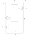
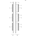
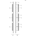
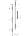
- FIG. 1 is a bottom view showing a configuration of a power transmission device according to a first embodiment of the present invention. It is front sectional drawing which shows the structure of the power transmission apparatus and power receiving apparatus which concern on 2nd Embodiment of this invention. It is front sectional drawing which shows the structure of the power transmission apparatus and power receiving apparatus which concern on 3rd Embodiment of this invention. It is front sectional drawing which shows the structure of the power transmission apparatus and power receiving apparatus which concern on 4th Embodiment of this invention. It is front sectional drawing which shows the structure of the power transmission apparatus and power receiving apparatus which concern on 5th Embodiment of this invention. It is front sectional drawing which shows the structure of the power transmission apparatus and power receiving apparatus which concern on 6th Embodiment of this invention. It is a figure which shows the basic composition of the electric power transmission apparatus of a general electric field coupling system.
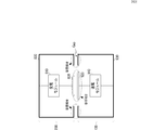
- FIG. 1 is a front sectional view showing a configuration of a power transmission device and a power reception device.
- FIG. 2 is a bottom view illustrating the configuration of the power transmission device. In each figure, only the electrode pattern is shown. Further, the configurations of the AC power supply and the load circuit are the same as those in FIG.
- the power transmitting apparatus 100 and the power receiving apparatus 200 constitute a wireless power transmission apparatus as shown in FIG.
- the power transmission device 100 includes an insulating resin 110, a passive electrode 120, an active electrode 130, and a conductive resin 140.
- the power receiving device 200 includes an insulating resin 210, a passive electrode 220, and an active electrode 230.
- the power receiving apparatus 200 is provided inside or on the surface of an electronic device such as a mobile phone, a tablet terminal, or a notebook PC, for example, and illustration of the electronic device is omitted in FIG.
- the insulating resin 110 is a first insulating resin formed in a flat plate shape.
- the insulating resin 110 is made of a material having high rigidity.
- the insulating resin 110 is made of, for example, polycarbonate resin or high-rigidity grade ABS. Therefore, the insulating resin 110 has high resistance to scratches.
- the insulating resin 110 may be configured to maintain the insulating property by oxidizing the surface of the base (alumite treatment). In this case, the thickness of the insulating resin is, for example, about 20 ⁇ m to 30 ⁇ m, and in addition to the effect of having high resistance to scratches, the effect that it can be further reduced can be obtained.
- the passive electrode 120 is a first passive electrode disposed on the first plane (the lower surface in FIG. 1) side of the insulating resin 110.
- the passive electrode 120 generates an electrostatic capacitance between the passive electrode 120 and the passive electrode 220 disposed to face the second plane side of the insulating resin 110.
- the passive electrode 120 has a lower potential than the active electrode 130 and may be connected to a reference potential.
- the active electrode 130 is a first active electrode disposed between the two passive electrodes 120 on the first plane side of the insulating resin 110.
- the active electrode 130 generates a capacitance between the active electrode 130 and the active electrode 230 disposed to face the second plane side of the insulating resin 110.
- the active electrode 130 has a higher potential than the passive electrode 120.
- the passive electrode 120 and the active electrode 130 have a rectangular shape when viewed from the bottom.
- the passive electrode 120 and the active electrode 130 are made of a metal body such as copper or aluminum.
- the passive electrode 120 is fixed to the insulating resin 110 with an adhesive or the like.
- the active electrode 130 is fixed to the conductive resin 140 with an adhesive or the like.
- the passive electrode 120 is electrically connected to the power transmission circuit via the connection part 121.
- the active electrode 130 is electrically connected to the power transmission circuit via the connection portion 131.
- the conductive resin 140 is a first conductive resin disposed between the insulating resin 110 and the active electrode 130.
- the conductive resin 140 is fixed to the insulating resin 110 with an adhesive or the like.
- the volume resistivity of the conductive resin 140 is several tens of ⁇ ⁇ cm to several k ⁇ ⁇ cm. Therefore, the conductive resin 140 has a predetermined conductivity as compared with the insulating resin 110.
- the insulating resin 210 is formed in a flat plate shape.
- the insulating resin 210 is made of a material having high rigidity.
- the insulating resin 210 is made of, for example, polycarbonate resin or high-rigidity grade ABS. Therefore, the insulating resin 210 has a high resistance to scratches.
- the passive electrode 220 is a second passive electrode disposed on the first plane (upper surface in FIG. 1) side of the insulating resin 210.
- the passive electrode 220 generates a capacitance between the passive electrode 120 and the passive electrode 120 disposed to face the second plane side of the insulating resin 210.
- the passive electrode 220 has a lower potential than the active electrode 230 and may be connected to a reference potential.
- the active electrode 230 is a second active electrode disposed between the passive electrodes 220 on the first plane of the insulating resin 210.
- the active electrode 230 generates a capacitance between the active electrode 230 and the active electrode 130 disposed to face the second plane side of the insulating resin 210.
- the active electrode 230 has a higher potential than the passive electrode 220. Strictly speaking, the peak value of the AC voltage generated between the active electrodes 130 and 230 is larger than the peak value of the AC voltage generated between the passive electrodes 120 and 220.
- the conductive resin 140 since the conductive resin 140 has a predetermined conductivity, the conductive resin 140 can be considered as a part of the active electrode 130 when considered as a capacitive element. That is, the interelectrode distance between the active electrode 130 and the active electrode 230 is only the sum of the thickness of the insulating resins 110 and 210 and the distance (interval) between the insulating resins 110 and 210. The generated inter-electrode distance is substantially shortened. Accordingly, since a large capacitance can be generated between the active electrode 130 and the active electrode 230, the power transmission efficiency between the active electrode 130 and the active electrode 230 can be reduced while suppressing the occurrence of discharge. I can give you.
- the conductive resin 140 is preferably made of a material softer than the insulating resin 110.
- the active electrode 130 can be protected by absorbing an impact on the active electrode 130.
- FIG. 3 is a front sectional view showing the configuration of the power transmission device and the power reception device.
- the power transmission device 100A further includes a conductive resin 150 in addition to the configuration of the power transmission device 100 shown in the first embodiment.
- the conductive resin 150 is a second conductive resin disposed between the insulating resin 110 and the passive electrode 120.
- the passive electrode 120 is fixed to the conductive resin 150 with an adhesive or the like.
- the conductive resin 150 is fixed to the insulating resin 110 with an adhesive or the like.
- the specific volume resistivity of the conductive resin 150 is several tens of ⁇ ⁇ cm to several k ⁇ ⁇ cm. Therefore, the conductive resin 150 has a predetermined conductivity as compared with the insulating resin 110.
- the conductive resin 150 is preferably made of a material softer than the insulating resin 110.
- the passive electrode 120 can be protected by absorbing an impact on the passive electrode 120.
- the thickness of the conductive resin 140 and the conductive resin 150 may be the same or different. When the thicknesses are different, it is preferable to make the conductive resin 140 thicker.
- FIG. 4 is a front sectional view showing the configuration of the power transmission device and the power reception device.
- the conductive resin 140 and the conductive resin 150 constituting the power transmission device 100B have conductivity in the thickness direction, and an anisotropic resin having no conductivity continues in a direction perpendicular to the thickness direction. It is configured.
- the insulation between the passive electrode 120 and the active electrode 130 can be ensured by the anisotropic resin having conductivity in the thickness direction of the conductive resin 140 and the conductive resin 150.
- the conductive resin 140 and the conductive resin 150 are made of one anisotropic resin, the structure of the conductive resin 140 and the conductive resin 150 is easy, and the conductive resin 140 and the conductive resin 150 can be easily manufactured.
- FIG. 5 is a front sectional view showing the configuration of the power transmission device and the power reception device.
- the power transmission device 100C further includes an insulating resin 160 in addition to the configuration of the power transmission device 100A shown in the second embodiment.
- the insulating resin 160 is a second insulating resin disposed between the conductive resin 140 and the conductive resin 150.
- the conductive resin 140, the conductive resin 150, and the insulating resin 160 are integrally molded.
- the insulating resin 160 is disposed between the conductive resin 140 and the conductive resin 150, the insulation between the passive electrode 120 and the active electrode 130 can be further ensured.
- the conductive resin 140, the conductive resin 150, and the insulating resin 160 are integrally molded, the conductive resin 140, the conductive resin 150, and the insulating resin 160 can be easily manufactured. .
- FIG. 6 is a front sectional view showing the configuration of the power transmission device and the power reception device.
- the conductive resin 150 ⁇ / b> D constituting the power transmission device 100 ⁇ / b> D is configured to have a resistance value lower than that of the conductive resin 140.
- the volume specific resistivity of the conductive resin 140 is several tens of ⁇ ⁇ cm to several k ⁇ ⁇ cm, whereas the volume specific resistivity of the conductive resin 150D is several ⁇ ⁇ cm. Therefore, the conductive resin 150 ⁇ / b> D has higher conductivity than the conductive resin 140.
- FIG. 7 is a front cross-sectional view illustrating the configuration of the power transmission device and the power reception device.
- the passive electrode 120 of the power transmission apparatus 100 and the passive electrode 220 of the power reception apparatus 200 do not necessarily overlap, and the active electrode 130 of the power transmission apparatus 100 and the active electrode 230 of the power reception apparatus 200 do not necessarily overlap. This is because the power transmission device 100 and the power reception device 200 may be misaligned.
- the design is such that the passive electrode 120 of the power transmission device 100 and the active electrode 230 of the power reception device 200 do not overlap, or the design is such that the active electrode 130 of the power transmission device 100 and the passive electrode 220 of the power reception device 200 do not overlap.
- the power transmission efficiency is extremely reduced.
- the passive electrode 120 and the active electrode 230 are controlled by controlling to stop power transmission between the respective electrodes. Between the active electrode 130 and the passive electrode 220 can be suppressed.
- the passive electrodes 120 and 220 are each exemplified by two electrodes having a rectangular shape in plan view. However, at least one of the passive electrodes 120 and 220 is provided around the active electrodes 130 and 230. It is also possible to use one made of a frame-shaped electrode that surrounds.
- the power receiving device 200 has been exemplified to include the insulating resin 210, the passive electrode 220 and the active electrode 230 may be exposed without being covered with the insulating resin 210.
- 1st conductive resin and 2nd conductive resin may be provided in the power receiving apparatus 200 side instead of the power transmission apparatus 100.
- the conductive resin 140 may be provided on the surface side of the active electrode 230 close to the power transmission device 100 without providing the conductive resin 140 in the power transmission device 100.
- the conductive resin 150 may not be provided in the power transmission device 100, and the conductive resin 150 may be further provided on the surface side of the passive electrode 220 close to the power transmission device 100.
Landscapes
- Engineering & Computer Science (AREA)
- Computer Networks & Wireless Communication (AREA)
- Power Engineering (AREA)
- Charge And Discharge Circuits For Batteries Or The Like (AREA)
- Physical Or Chemical Processes And Apparatus (AREA)
Abstract
Description
110-絶縁性樹脂(第1絶縁性樹脂)
120-パッシブ電極(第1パッシブ電極)
130-アクティブ電極(第1アクティブ電極)
140-導電性樹脂(第1導電性樹脂)
150-導電性樹脂(第2導電性樹脂)
160-絶縁性樹脂(第2絶縁性樹脂)
200-受電装置
220-パッシブ電極(第2パッシブ電極)
230-アクティブ電極(第2アクティブ電極)
Claims (10)
- 第1アクティブ電極、第1パッシブ電極ならびに前記第1アクティブ電極および前記第1パッシブ電極に接続され交流電圧を供給する送電回路を有する送電装置と、
前記第1アクティブ電極と結合する第2アクティブ電極、前記第1パッシブ電極と結合する第2パッシブ電極ならびに前記第2アクティブ電極および前記第2パッシブ電極に接続され負荷回路へ電力を供給する受電回路を有する受電装置と、
を備えたワイヤレス電力伝送装置において、
平板状に形成された第1絶縁性樹脂と、
前記第1絶縁性樹脂の第1平面側に配される第1導電性樹脂と、
を備え、
前記第1パッシブ電極は、前記第1絶縁性樹脂の第1平面側に配され、
前記第2パッシブ電極は、前記第1絶縁性樹脂の第2平面側において前記第1パッシブ電極と対向するように配され、
前記第1アクティブ電極は、前記第1導電性樹脂を介して、前記第1絶縁性樹脂の第1平面側に配され、
前記第2アクティブ電極は、前記第1絶縁性樹脂の第2平面側において前記第1アクティブ電極と対向するように配されたことを特徴とするワイヤレス電力伝送装置。 - 第1アクティブ電極、第1パッシブ電極ならびに前記第1アクティブ電極および前記第1パッシブ電極に接続され負荷回路へ電力を供給する受電回路を有する受電装置と、
前記第1アクティブ電極と結合する第2アクティブ電極、前記第1パッシブ電極と結合する第2パッシブ電極ならびに前記第2アクティブ電極および前記第2パッシブ電極に接続され交流電圧を供給する送電回路を有する送電装置と、
を備えたワイヤレス電力伝送装置において、
平板状に形成された第1絶縁性樹脂と、
前記第1絶縁性樹脂の第1平面側に配される第1導電性樹脂と、
を備え、
前記第1パッシブ電極は、前記第1絶縁性樹脂の第1平面側に配され、
前記第2パッシブ電極は、前記第1絶縁性樹脂の第2平面側において前記第1パッシブ電極と対向するように配され、
前記第1アクティブ電極は、前記第1導電性樹脂を介して、前記第1絶縁性樹脂の第1平面側に配され、
前記第2アクティブ電極は、前記第1絶縁性樹脂の第2平面側において前記第1アクティブ電極と対向するように配されたことを特徴とするワイヤレス電力伝送装置。 - 前記第1導電性樹脂は、前記第1絶縁性樹脂よりも柔らかい素材で構成された、請求項1または2に記載のワイヤレス電力伝送装置。
- 前記第1絶縁性樹脂と前記第1パッシブ電極との間に配される第2導電性樹脂をさらに備えた、請求項1~3のいずれかに記載のワイヤレス電力伝送装置。
- 前記第2導電性樹脂は、前記第1絶縁性樹脂よりも柔らかい素材で構成された、請求項4に記載のワイヤレス電力伝送装置。
- 前記第1導電性樹脂および前記第2導電性樹脂は、その厚み方向に導電性を有する異方性樹脂が連続して構成されたものである、請求項4または5に記載のワイヤレス電力伝送装置。
- 前記第1絶縁性樹脂の第1平面側において、前記第1導電性樹脂と前記第2導電性樹脂との間に配される第2絶縁性樹脂をさらに備え、
前記第1導電性樹脂、前記第2導電性樹脂および前記第2絶縁性樹脂は、一体成型されたものである、請求項4~6のいずれか1項に記載のワイヤレス電力伝送装置。 - 前記第2導電性樹脂は、前記第1導電性樹脂よりも抵抗値が低く構成された、請求項4~7のいずれか1項に記載のワイヤレス電力伝送装置。
- 第1アクティブ電極、第1パッシブ電極ならびに前記第1アクティブ電極および前記第1パッシブ電極に接続され交流電圧を供給する送電回路を備えたワイヤレス電力伝送装置用の送電装置において、
平板状に形成された第1絶縁性樹脂と、
前記第1絶縁性樹脂の第1平面側に配される第1導電性樹脂と、
を備え、
前記第1パッシブ電極は、前記第1絶縁性樹脂の第1平面側に配され、
前記第1アクティブ電極は、前記第1導電性樹脂を介して、前記第1絶縁性樹脂の第1平面側に配されたことを特徴とする送電装置。 - 第1アクティブ電極、第1パッシブ電極ならびに前記第1アクティブ電極および前記第1パッシブ電極に接続され負荷回路へ電力を供給する受電回路を備えたワイヤレス電力伝送装置用の受電装置において、
平板状に形成された第1絶縁性樹脂と、
前記第1絶縁性樹脂の第1平面側に配される第1導電性樹脂と、
を備え、
前記第1パッシブ電極は、前記第1絶縁性樹脂の第1平面側に配され、
前記第1アクティブ電極は、前記第1導電性樹脂を介して、前記第1絶縁性樹脂の第1平面側に配されたことを特徴とする受電装置。
Priority Applications (2)
| Application Number | Priority Date | Filing Date | Title |
|---|---|---|---|
| CN201390001046.4U CN204809992U (zh) | 2013-01-11 | 2013-09-03 | 无线电力传输装置和用在其中的送电装置以及受电装置 |
| JP2014556320A JP6135679B2 (ja) | 2013-01-11 | 2013-09-03 | ワイヤレス電力伝送装置 |
Applications Claiming Priority (2)
| Application Number | Priority Date | Filing Date | Title |
|---|---|---|---|
| JP2013003379 | 2013-01-11 | ||
| JP2013-003379 | 2013-01-11 |
Publications (1)
| Publication Number | Publication Date |
|---|---|
| WO2014109093A1 true WO2014109093A1 (ja) | 2014-07-17 |
Family
ID=51166758
Family Applications (1)
| Application Number | Title | Priority Date | Filing Date |
|---|---|---|---|
| PCT/JP2013/073612 Ceased WO2014109093A1 (ja) | 2013-01-11 | 2013-09-03 | ワイヤレス電力伝送装置ならびにこれに用いる送電装置および受電装置 |
Country Status (3)
| Country | Link |
|---|---|
| JP (1) | JP6135679B2 (ja) |
| CN (1) | CN204809992U (ja) |
| WO (1) | WO2014109093A1 (ja) |
Families Citing this family (1)
| Publication number | Priority date | Publication date | Assignee | Title |
|---|---|---|---|---|
| JP7067440B2 (ja) * | 2018-11-26 | 2022-05-16 | 株式会社村田製作所 | セルバランス制御装置 |
Citations (3)
| Publication number | Priority date | Publication date | Assignee | Title |
|---|---|---|---|---|
| JP2011259649A (ja) * | 2010-06-11 | 2011-12-22 | Takenaka Komuten Co Ltd | 非接触電力供給システムのための電極構造、及び非接触電力供給システム |
| JP2012210146A (ja) * | 2009-06-25 | 2012-10-25 | Murata Mfg Co Ltd | 電力伝送システム |
| JP2012231661A (ja) * | 2011-04-15 | 2012-11-22 | Semiconductor Energy Lab Co Ltd | 発光装置、表示装置、発光システム及び表示システム |
-
2013
- 2013-09-03 WO PCT/JP2013/073612 patent/WO2014109093A1/ja not_active Ceased
- 2013-09-03 JP JP2014556320A patent/JP6135679B2/ja active Active
- 2013-09-03 CN CN201390001046.4U patent/CN204809992U/zh not_active Expired - Lifetime
Patent Citations (3)
| Publication number | Priority date | Publication date | Assignee | Title |
|---|---|---|---|---|
| JP2012210146A (ja) * | 2009-06-25 | 2012-10-25 | Murata Mfg Co Ltd | 電力伝送システム |
| JP2011259649A (ja) * | 2010-06-11 | 2011-12-22 | Takenaka Komuten Co Ltd | 非接触電力供給システムのための電極構造、及び非接触電力供給システム |
| JP2012231661A (ja) * | 2011-04-15 | 2012-11-22 | Semiconductor Energy Lab Co Ltd | 発光装置、表示装置、発光システム及び表示システム |
Also Published As
| Publication number | Publication date |
|---|---|
| JP6135679B2 (ja) | 2017-05-31 |
| JPWO2014109093A1 (ja) | 2017-01-19 |
| CN204809992U (zh) | 2015-11-25 |
Similar Documents
| Publication | Publication Date | Title |
|---|---|---|
| JP5403073B2 (ja) | 電力受電装置及び電力送電装置 | |
| JP5093369B2 (ja) | 送電装置、受電装置および電力伝送システム | |
| US9461507B2 (en) | Wireless power transmission system | |
| JP5152298B2 (ja) | 送電装置、受電装置及びワイヤレス電力伝送システム | |
| JP5168438B2 (ja) | 電力伝送システム、及び受電ジャケット | |
| JP5737482B2 (ja) | ワイヤレス受電装置、ワイヤレス送電装置、及びワイヤレス送受電装置 | |
| JP5979301B2 (ja) | 送電装置および受電装置 | |
| CN103376591A (zh) | 彩色滤光基板以及具有该彩色滤光基板的显示面板 | |
| US9673658B2 (en) | Non-contact capacitive coupling type power charging apparatus and non-contact capacitive coupling type battery apparatus | |
| KR101771747B1 (ko) | 공통모드필터 | |
| JPWO2013168307A1 (ja) | ワイヤレス電力伝送システム | |
| JP6135679B2 (ja) | ワイヤレス電力伝送装置 | |
| WO2014125731A1 (ja) | ワイヤレス電力伝送システム | |
| TWM532686U (zh) | 一種二次電池 | |
| JP6265543B2 (ja) | 発電装置 | |
| JP5772501B2 (ja) | 電力伝送システム | |
| TWI565399B (zh) | Anti - electromagnetic interference structure of wireless power transmission device | |
| WO2015052003A1 (en) | Wireless capacitive power receiving module | |
| WO2021148585A1 (en) | Position-free, multiple output capacitive power transfer system | |
| KR102029496B1 (ko) | 유도 코일 축전기 | |
| KR101670127B1 (ko) | 비접촉 방식 충전 장치 및 비접촉 방식 배터리 장치 | |
| WO2016177057A1 (zh) | 设备外壳、设备、充电座及无线充电方法 |
Legal Events
| Date | Code | Title | Description |
|---|---|---|---|
| WWE | Wipo information: entry into national phase |
Ref document number: 201390001046.4 Country of ref document: CN |
|
| 121 | Ep: the epo has been informed by wipo that ep was designated in this application |
Ref document number: 13870797 Country of ref document: EP Kind code of ref document: A1 |
|
| ENP | Entry into the national phase |
Ref document number: 2014556320 Country of ref document: JP Kind code of ref document: A |
|
| NENP | Non-entry into the national phase |
Ref country code: DE |
|
| 122 | Ep: pct application non-entry in european phase |
Ref document number: 13870797 Country of ref document: EP Kind code of ref document: A1 |