WO2014104105A1 - 光学素子 - Google Patents
光学素子 Download PDFInfo
- Publication number
- WO2014104105A1 WO2014104105A1 PCT/JP2013/084692 JP2013084692W WO2014104105A1 WO 2014104105 A1 WO2014104105 A1 WO 2014104105A1 JP 2013084692 W JP2013084692 W JP 2013084692W WO 2014104105 A1 WO2014104105 A1 WO 2014104105A1
- Authority
- WO
- WIPO (PCT)
- Prior art keywords
- liquid crystal
- optical element
- region
- resin layer
- refractive index
- Prior art date
Links
Images


Classifications
-
- G—PHYSICS
- G02—OPTICS
- G02B—OPTICAL ELEMENTS, SYSTEMS OR APPARATUS
- G02B6/00—Light guides; Structural details of arrangements comprising light guides and other optical elements, e.g. couplings
- G02B6/02—Optical fibres with cladding with or without a coating
- G02B6/024—Optical fibres with cladding with or without a coating with polarisation maintaining properties
-
- G—PHYSICS
- G01—MEASURING; TESTING
- G01N—INVESTIGATING OR ANALYSING MATERIALS BY DETERMINING THEIR CHEMICAL OR PHYSICAL PROPERTIES
- G01N21/00—Investigating or analysing materials by the use of optical means, i.e. using sub-millimetre waves, infrared, visible or ultraviolet light
-
- G—PHYSICS
- G01—MEASURING; TESTING
- G01N—INVESTIGATING OR ANALYSING MATERIALS BY DETERMINING THEIR CHEMICAL OR PHYSICAL PROPERTIES
- G01N21/00—Investigating or analysing materials by the use of optical means, i.e. using sub-millimetre waves, infrared, visible or ultraviolet light
- G01N21/17—Systems in which incident light is modified in accordance with the properties of the material investigated
- G01N21/55—Specular reflectivity
- G01N21/552—Attenuated total reflection
- G01N21/553—Attenuated total reflection and using surface plasmons
-
- G—PHYSICS
- G02—OPTICS
- G02B—OPTICAL ELEMENTS, SYSTEMS OR APPARATUS
- G02B6/00—Light guides; Structural details of arrangements comprising light guides and other optical elements, e.g. couplings
- G02B6/10—Light guides; Structural details of arrangements comprising light guides and other optical elements, e.g. couplings of the optical waveguide type
- G02B6/12—Light guides; Structural details of arrangements comprising light guides and other optical elements, e.g. couplings of the optical waveguide type of the integrated circuit kind
- G02B6/122—Basic optical elements, e.g. light-guiding paths
- G02B6/1226—Basic optical elements, e.g. light-guiding paths involving surface plasmon interaction
-
- G—PHYSICS
- G02—OPTICS
- G02B—OPTICAL ELEMENTS, SYSTEMS OR APPARATUS
- G02B6/00—Light guides; Structural details of arrangements comprising light guides and other optical elements, e.g. couplings
- G02B6/10—Light guides; Structural details of arrangements comprising light guides and other optical elements, e.g. couplings of the optical waveguide type
- G02B6/12—Light guides; Structural details of arrangements comprising light guides and other optical elements, e.g. couplings of the optical waveguide type of the integrated circuit kind
- G02B6/126—Light guides; Structural details of arrangements comprising light guides and other optical elements, e.g. couplings of the optical waveguide type of the integrated circuit kind using polarisation effects
-
- G—PHYSICS
- G02—OPTICS
- G02B—OPTICAL ELEMENTS, SYSTEMS OR APPARATUS
- G02B6/00—Light guides; Structural details of arrangements comprising light guides and other optical elements, e.g. couplings
- G02B6/10—Light guides; Structural details of arrangements comprising light guides and other optical elements, e.g. couplings of the optical waveguide type
- G02B6/12—Light guides; Structural details of arrangements comprising light guides and other optical elements, e.g. couplings of the optical waveguide type of the integrated circuit kind
- G02B2006/12166—Manufacturing methods
- G02B2006/12169—Annealing
- G02B2006/12171—Annealing using a laser beam
-
- G—PHYSICS
- G02—OPTICS
- G02B—OPTICAL ELEMENTS, SYSTEMS OR APPARATUS
- G02B6/00—Light guides; Structural details of arrangements comprising light guides and other optical elements, e.g. couplings
- G02B6/10—Light guides; Structural details of arrangements comprising light guides and other optical elements, e.g. couplings of the optical waveguide type
- G02B6/12—Light guides; Structural details of arrangements comprising light guides and other optical elements, e.g. couplings of the optical waveguide type of the integrated circuit kind
- G02B6/13—Integrated optical circuits characterised by the manufacturing method
- G02B6/138—Integrated optical circuits characterised by the manufacturing method by using polymerisation
-
- G—PHYSICS
- G02—OPTICS
- G02F—OPTICAL DEVICES OR ARRANGEMENTS FOR THE CONTROL OF LIGHT BY MODIFICATION OF THE OPTICAL PROPERTIES OF THE MEDIA OF THE ELEMENTS INVOLVED THEREIN; NON-LINEAR OPTICS; FREQUENCY-CHANGING OF LIGHT; OPTICAL LOGIC ELEMENTS; OPTICAL ANALOGUE/DIGITAL CONVERTERS
- G02F1/00—Devices or arrangements for the control of the intensity, colour, phase, polarisation or direction of light arriving from an independent light source, e.g. switching, gating or modulating; Non-linear optics
- G02F1/01—Devices or arrangements for the control of the intensity, colour, phase, polarisation or direction of light arriving from an independent light source, e.g. switching, gating or modulating; Non-linear optics for the control of the intensity, phase, polarisation or colour
- G02F1/13—Devices or arrangements for the control of the intensity, colour, phase, polarisation or direction of light arriving from an independent light source, e.g. switching, gating or modulating; Non-linear optics for the control of the intensity, phase, polarisation or colour based on liquid crystals, e.g. single liquid crystal display cells
- G02F1/1326—Liquid crystal optical waveguides or liquid crystal cells specially adapted for gating or modulating between optical waveguides
Definitions
- the present invention relates to an optical element having a resin layer and an optical waveguide region formed in the resin layer.
- Patent Document 1 discloses that an optical fiber including a liquid crystal-filled optical fiber filled with liquid crystal in a hole of a holey fiber is applied by applying a magnetic field to the filled liquid crystal to change the alignment state of the liquid crystal.
- An optical fiber system for controlling transmission characteristics is described.
- Non-Patent Document 1 describes a capillary optical fiber having an annular high refractive index optical core around a vent hole, a low refractive index optical cladding, and a high refractive index coating layer. Has been.
- a conventional optical waveguide made of a resin material is isotropic or has anisotropy oriented only in one specific direction. For this reason, in such an optical waveguide, it is impossible to propagate radial polarization or azimuth polarization while maintaining the polarization direction.
- Radial polarized light here is light in which the polarization direction is radially distributed in the radial direction in a plane perpendicular to the traveling direction.
- azimuth polarization is light in which the polarization direction is distributed in the circumferential direction in a plane perpendicular to the traveling direction.
- an optical waveguide having a radially oriented structure can cope with radial polarization or azimuth polarization, but it is difficult to easily produce such an optical waveguide. Accordingly, an object of the present invention is to provide an optical element having an optical waveguide region capable of propagating radial polarization or azimuth polarization while maintaining the polarization direction.
- the optical element has a resin layer and an optical waveguide region that is formed in the resin layer and in which light is guided in the longitudinal direction of the resin layer.
- the liquid crystal In the optical waveguide region, the liquid crystal is substantially radially in a cross section perpendicular to the longitudinal direction.
- the molecules are oriented, and the refractive index of the optical waveguide region is larger than the refractive index of the resin layer.
- the optical element further includes a tubular space having a substantially circular cross section formed in the resin layer, and the optical waveguide region is formed so as to be in contact with the tubular space, and the optical waveguide region has a substantially circular shape. It is preferable that the liquid crystal molecules are aligned substantially radially along the radial direction of the cross section.
- optical element it is possible to propagate radial polarization or azimuth polarization while maintaining the polarization direction.
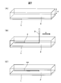
- FIG. 1 is a schematic diagram of an optical element 10.
- FIG. (A) to (C) are schematic views for explaining a method of manufacturing the optical element 10.
- 3 is a flowchart showing a method for manufacturing the optical element 10.
- FIG. 6 is a schematic diagram for explaining a formation position and a size of a cavity 14.
- (A) to (D) are photographs when a surface parallel to the longitudinal direction of the optical element 10 is observed with a polarizing microscope.
- (A) to (D) are photographs when a cross section perpendicular to the longitudinal direction of the optical element 10 is observed with a polarizing microscope.
- (A) to (D) are photographs when a cross section perpendicular to the longitudinal direction of the optical element 10 is observed with a polarizing microscope.
- FIG. (A) And (B) is a figure for demonstrating the conditions of the waveguide simulation of the optical element 10.
- FIG. (A)-(D) are the figures which showed the result of the waveguide simulation in case the center area
- (A) to (D) are diagrams showing the results of a waveguide simulation when the central region 34 is filled with water.
- (A) And (B) is a figure for demonstrating the SPR sensor to which the optical element 10 is applied.
- FIG. 1 is a schematic diagram of the optical element 10.
- the optical element 10 has a resin layer 12 as a cladding portion of the optical waveguide region.
- an acrylic resin is used as the resin layer 12.
- a cavity 14 is formed in the resin layer 12 as a tubular space having a substantially circular cross section.
- substantially circular refers to a shape having no sharp portion or dent, such as a rectangle, and the ratio of the difference between the maximum diameter and the minimum diameter with respect to the maximum diameter is, for example, 10% or less.
- the optical element 10 has a liquid crystal region 15 formed in the resin layer 12 in a portion (near the boundary) in contact with the cavity 14 as a core portion of the optical waveguide region.
- a P-type liquid crystal is used as the liquid crystal.
- the liquid crystal molecules are aligned substantially radially along the radial direction of the cavity 14 having a substantially circular cross section.
- the alignment of the liquid crystal molecules is represented by a large number of ellipses 15 ⁇ / b> A arranged substantially radially in the radial direction in a substantially circular cross section with the cavity 14 as the center.
- substantially radial refers to a state in which the outer side of the resin layer 12 extends from the central cavity 14 as a whole. For this reason, the liquid crystal molecules do not necessarily have to be strictly radially aligned in the entire liquid crystal region 15.
- the liquid crystal region 15 functions as an optical waveguide region, and light can propagate in the liquid crystal region 15. Since the liquid crystal region 15 has a larger refractive index than that of the resin layer 12, a difference in refractive index can be made between the resin layer 12 and the liquid crystal region 15. Therefore, when light enters the liquid crystal region 15, the light traveling from the liquid crystal region 15 toward the resin layer 12 outside the liquid crystal region 15 at a small incident angle is totally reflected by the boundary surface 16 between the liquid crystal region 15 and the resin layer 12.
- the liquid crystal region 15 has a larger refractive index than the inner cavity 14, a difference in refractive index can be made between the cavity 14 and the liquid crystal region 15. Therefore, the light traveling from the liquid crystal region 15 to the inner cavity 14 at a small incident angle is also totally reflected at the boundary surface between the liquid crystal region 15 and the cavity 14. Thus, since the light propagates in the liquid crystal region 15 (see arrow A in FIG. 1), the optical element 10 can confine the light in the liquid crystal region 15.
- the optical element 10 can be used particularly as a GI (graded-index) waveguide.
- the boundary surface 16 between the resin layer 12 and the liquid crystal region 15 is shown for the sake of explanation, but it is considered that this boundary surface 16 is not clearly defined in practice.
- the light propagating in the liquid crystal region 15 is reflected and propagates in the liquid crystal region 15 before reaching the region having a smaller refractive index outside the liquid crystal region 15.
- FIGS. 2A to 2C are schematic views for explaining a method for manufacturing the optical element 10.
- FIG. 3 is a flowchart showing a method for manufacturing the optical element 10. Each step of the manufacturing method will be described with reference to FIGS.
- a substrate 1 is prepared, and an uncured curable resin 2 layer is formed on the substrate 1 (S1).
- This layer corresponds to the resin layer 12 in FIG. Since the curable resin 2 has fluidity in an uncured state, a frame (not shown) surrounding the periphery is prepared, and the curable resin 2 is injected into the frame.
- an acrylic resin that is an ultraviolet curable resin is used as the curable resin 2.
- a thermosetting resin may be used as the curable resin 2.
- the thickness d of the curable resin 2 may be about 1000 ⁇ m.
- a needle 3 that can inject liquid crystal is inserted into the curable resin 2 (S2).
- the needle 3 is hollow and has a sharp shape toward the tip like an injection needle, and has an opening (not shown) at the tip.
- the depth at which the needle 3 is inserted is, for example, about half of the thickness d of the curable resin 2.
- the liquid crystal 4 is injected into the curable resin 2 through the needle 3 while moving the needle 3 (S3).
- a P-type liquid crystal is used as the liquid crystal 4.
- the needle 3 is translated along the X direction shown in FIG.
- the liquid crystal 4 is injected into the layer of the curable resin 2 from the opening at the tip of the needle 3 by applying pressure from above the needle 3 while moving the needle 3.
- the liquid crystal 4 has a substantially circular cross section perpendicular to the X direction due to surface tension.
- the needle 3 is removed from the curable resin 2 (S4).
- the curable resin 2 is not yet cured, when the needle 3 is extracted, the hole formed in the curable resin 2 is closed by the needle 3.
- the liquid crystal 4 is confined in the curable resin 2 and is arranged in a tubular shape.
- the curable resin 2 is cured by ultraviolet irradiation, and the liquid crystal 4 is confined in the curable resin 2.
- a portion where the liquid crystal 4 exists is set as a liquid crystal flow path 4A (S5).
- the curable resin 2 is cured by heating.
- a channel 4A having a substantially circular cross section is formed in the tubular region into which the liquid crystal 4 is injected.
- the liquid crystal 4 may penetrate into the curable resin 2 even before the curable resin 2 is cured, the liquid crystal 4 remains in the flow path 4A immediately after the curing. Therefore, the liquid crystal 4 is left in this state for a certain period of time and the immersion of the liquid crystal 4 into the layer of the curable resin 2 is completed (S6). Over time, the liquid crystal 4 diffuses into the resin due to the concentration gradient at the interface between the liquid crystal 4 and the curable resin 2, and the liquid crystal molecules are aligned in the diffusion direction as shown in FIG. Resin chains are fixed by curing, and liquid crystal molecules enter between them, thereby obtaining a region (liquid crystal region 15 in FIG. 1) in which liquid crystal molecules are aligned substantially radially around the channel 4A. When the liquid crystal 4 disappears from the flow path 4A, the area of the flow path 4A becomes the cavity 14 of FIG.
- the liquid crystal 4 When the liquid crystal 4 is completely confined in the curable resin 2, depending on the type of the liquid crystal 4, it takes about several days to penetrate into the resin. On the other hand, when the hole due to the needle 3 is not blocked and remains open, or when the liquid crystal 4 comes into contact with the outside air by intentionally making a hole in the layer of the curable resin 2, the liquid crystal 4 becomes faster. Soak in the resin.
- the liquid crystal 4 remains in the flow path 4A even after a lapse of a certain time, a part of the curable resin 2 is cut out and the liquid crystal 4 confined in the curable resin 2 is extracted. Even when the flow path 4A becomes hollow, a part of the curable resin 2 is cut out to clean the inside of the flow path 4A (S7).
- the cavity 14 and the liquid crystal region 15 of FIG. 1 are formed in the layer of the curable resin 2, and the optical element 10 of FIG. 1 is obtained.
- the optical element 10 of FIG. 1 can be obtained when the acrylic resin is used as the curable resin 2 and the P-type liquid crystal is used as the liquid crystal 4 and each step of FIG. 3 is executed.
- some combinations of resin and liquid crystal cannot form the substantially circular flow path 4A, or some liquid crystals do not diffuse radially in the resin.
- the injected liquid crystal 4 may float on the surface of the resin layer depending on the viscosity of the curable resin 2 or the difference in density between the curable resin 2 and the liquid crystal 4.
- the liquid crystal 4 is often a mixture composed of a plurality of compounds, and the diffusion coefficient varies depending on the components.
- the curable resin 2 and the liquid crystal 4 can inject the liquid crystal 4 into the inside of the curable resin 2 in the relationship between the viscosity and the density, and the liquid crystal 4 is diffused into the curable resin 2 to be approximately It is necessary to select a combination that is oriented radially.
- the optical element 10 can be obtained even if the liquid crystal is injected into the cavity already formed in the resin. Can be obtained. Therefore, another method for manufacturing the optical element 10 will also be described.
- a resin layer in which a cavity having a substantially circular cross section is formed in advance is prepared. Then, a needle is inserted into the resin, liquid crystal is injected into the cavity, and the needle is removed. Thereafter, the same steps as S6 and S7 in FIG. 3 are performed. That is, the liquid crystal is immersed in the resin over a certain period of time, and then a part of the resin layer is cut off to clean the inside of the cavity into which the liquid crystal has been injected.
- the optical element 10 is obtained also by the above process.
- the material of the resin layer 12 of the optical element 10 may be, for example, another ultraviolet curable resin such as an epoxy resin, or a thermosetting resin such as a urea resin, a melamine resin, or a phenol resin.
- the refractive index of the acrylic resin used in this experiment is 1.50, and the refractive index of the P-type liquid crystal MLC-7018 made by Merck is 1.55 for the extraordinary light refractive index ne and 1.47 for the ordinary light refractive index no. is there.
- the extraordinary light refractive index ne is larger than the refractive index of the acrylic resin, radial polarized light that is polarized parallel to the ne direction of the liquid crystal molecules aligned in a substantially radial direction is propagated.
- the extraordinary refractive index ne of the liquid crystal is 1.77 and the ordinary refractive index no is 1.54. Since these have a refractive index greater than 1.50 of the acrylic resin, both the intrinsic polarization of extraordinary rays and the intrinsic polarization of ordinary rays have a light confinement effect in accordance with the orientation of the liquid crystal, so that radial polarization or azimuth polarization can be propagated.
- FIG. 4 is a schematic diagram for explaining the formation position and size of the cavity 14 formed in this experiment.
- the thickness of the resin layer 12 was 1000 ⁇ m, and the needle 3 was inserted into the resin layer 12 to a depth of 500 ⁇ m. Then, while the needle 3 is moved linearly along the surface direction of the resin layer 12 at a speed of 20 mm / sec, a dispensing pressure of 10 kPa is applied so that a substantially circular cavity 14 having a diameter of 200 ⁇ m is formed.
- Dispense type LCD Dispense type LCD.
- the flow path was formed by hardening the resin layer 12 with ultraviolet rays. Two such resin layers 12 were prepared, one provided an opening in the formed flow path, and the other left the liquid crystal inside completely sealed. Then, the liquid crystal was immersed in the resin layer 12 for several days. In this experiment, the diameter of the flow path (cavity 14) is made larger than when used as an optical element.
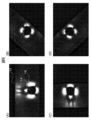
- FIGS. 5 (A) to 5 (D) are photographs when a surface parallel to the longitudinal direction of the optical element 10 manufactured as described above is observed with a polarizing microscope.
- 5A and 5B are photographs when the angle of the optical element 10 in the longitudinal direction is 0 ° with respect to the polarizing plate angle of 45 °.
- 5C and 5D are photographs when the angle of the optical element 10 in the longitudinal direction is 45 ° with respect to the polarizing plate angle of 45 °.
- FIG. 5A shows a resin layer 12 in which an opening (not shown) is provided in the flow path 4A so that liquid crystal is immersed therein.
- the liquid crystal soaks into the resin layer 12 and volatilizes, and the flow path 4A is hollowed out. It can be seen that the inside of the liquid crystal region 15 outside the channel 4A is bright and light is transmitted. It can also be seen that the liquid crystal penetrates to a depth as large as the diameter of the flow path 4 ⁇ / b> A, and there is a concentration gradient outside the liquid crystal region 15.
- FIG. 5B shows the resin layer 12 that has been immersed while the liquid crystal 4 is completely enclosed.
- the liquid crystal 4 penetrates into the resin layer 12 and remains in the flow path 4A. It can be seen that light is transmitted not only in the liquid crystal region 15 outside the channel 4A but also inside the channel 4A. As in FIG. 5A, it can be seen that the liquid crystal penetrates to the same depth as the diameter of the flow path 4A, and there is a concentration gradient outside the liquid crystal region 15.
- FIG. 5C is a photograph of the resin layer 12 of FIG. 5A when the longitudinal direction of the optical element 10 is inclined at an angle of 45 °.
- light is not transmitted through the liquid crystal region 15 through which light is transmitted when the longitudinal angle of the optical element 10 is 0 °.
- FIG. 5D is a photograph of the resin layer 12 of FIG. 5B when the longitudinal direction of the optical element 10 is inclined at an angle of 45 °. In the portion of the flow path 4A, light is transmitted as in FIG. 5B when the longitudinal angle of the optical element 10 is 0 °, but the liquid crystal region 15 does not transmit light.
- both the hollow channel and the channel in which the liquid crystal 4 remains are formed between the polarizing plate and the longitudinal direction of the optical element 10 in the liquid crystal region 15 near the boundary with the channel 4A.
- Light is transmitted when the angle is 45 °, and light is not transmitted when the angle between the polarizing plate and the longitudinal direction of the optical element 10 is 0 °. From this, it can be seen that in the liquid crystal region 15, the liquid crystal molecules are immersed with high orientation.
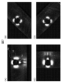
- FIGS. 7 (A) to 7 (D) are views when a cross section perpendicular to the longitudinal direction of the optical element 10 manufactured as described above is observed with a polarizing microscope. It is a photograph. 6 (A) to 6 (D) and FIGS. 7 (A) to 7 (D) show the optical element 10 at 0 °, 45 °, 90 °, 135 °, 180 °, 225 °, and 270 °, respectively. It is a photograph when rotated to 315 °.
- the resin layer 12 was the same as that shown in FIG. At any rotation angle, in the liquid crystal region 15 near the boundary with the cavity 14, light is not transmitted through only 45 ° and 135 ° linear directions with respect to the horizontal line, but it is dark, but in other portions, light is not transmitted. It can be seen that it is transparent. Since the transmission pattern does not change depending on the rotation angle of the optical element 10, it is presumed that the liquid crystal molecules are aligned substantially radially in the liquid crystal region 15.
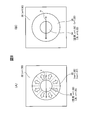
- FIGS. 8A and 8B are diagrams for explaining the conditions of the waveguide simulation of the optical element 10.
- the rectangular region to be subjected to the waveguiding simulation includes a central region 34, an annular region 35 surrounding the central region 34, and an outside of the annular region 35. And an outer region 32.
- the central region 34, the annular region 35, and the outer region 32 correspond to the cavity 14, the liquid crystal region 15, and the resin layer 12 of the optical element 10, respectively.
- the setting of the refractive index of the central region 34 and the outer region 32 is the same in FIGS. 8A and 8B.
- TE wave single-wavelength plane wave whose polarization direction is the direction of arrow a is used in both cases of FIG. 8 (A) and FIG. 8 (B).
- FIGS. 9A to 9D are diagrams showing the results of a waveguide simulation when the central region 34 is a cavity.
- 9A and 9B show the results under the conditions shown in FIG. 8A
- FIGS. 9C and 9D show the results under the conditions shown in FIG. 8B. It is a result.
- 9A and 9C the portion corresponding to the annular region 35 is indicated by a broken line.
- the electric field strength of the right and left portions of the annular region 35 is the highest. That is, light is confined in an annular region 35 having a high refractive index, and in particular, an annular region 35 in which the alignment direction of liquid crystal molecules is parallel to the polarization direction of incident light (the direction of arrow a in FIG. 8A). It can be seen that light is guided in the right and left portions of the.
- FIGS. 9C and 9D when there is no orientation, the electric field strength is uniformly high in the annular region 35. That is, it can be seen that light is guided over the entire circumference of the annular region 35 having a high refractive index.
- FIGS. 10 (A) to 10 (D) are diagrams showing the results of a waveguide simulation when the central region 34 is filled with water.
- FIGS. 10A and 10B show the results under the conditions shown in FIG. 8A
- FIGS. (D) shows the results under the conditions shown in FIG.
- FIGS. 10A and 10C a portion corresponding to the annular region 35 is indicated by a broken line.
- the optical element 10 has a structure in which liquid crystal molecules are aligned substantially radially along the radial direction of the substantially circular cross section of the cavity 14 that is a tubular space. Thereby, the optical element 10 can propagate the radially polarized light polarized along the alignment of the liquid crystal molecules while maintaining the polarization direction. Further, the optical element 10 uses a liquid crystal material in which both the extraordinary refractive index and the ordinary refractive index are larger than the refractive index of the surrounding cladding portion, so that the optical element 10 has a 90 ° angle with respect to the liquid crystal molecules aligned radially in the radial direction. Azimuth-polarized light polarized in the circumferential direction that forms an angle can also be propagated while maintaining the polarization direction.
- optical element 10 there is a refractive index sensor (SPR sensor) using a surface plasmon resonance phenomenon.
- SPR sensor refractive index sensor
- Surface plasmon resonance absorbs light with a wavelength and angle corresponding to the refractive index of the medium in contact with the metal thin film when light is incident on the inner surface of the metal thin film in contact with the medium at a total reflection angle or more. It is a phenomenon.
- FIG. 11A and FIG. 11B are diagrams for explaining an SPR sensor to which the optical element 10 is applied.
- FIG. 11A shows an example of a conventional waveguide type SPR sensor 20.
- the SPR sensor 20 has an optical waveguide 22 provided with a metal thin film 21 on the upper surface.
- the sample S to be measured is placed on the metal thin film 21 and light is incident from the incident surface 23 of the optical waveguide 22.
- Light propagates while repeating total reflection in the optical waveguide 22 and attenuates according to the refractive index of the sample S. For this reason, the refractive index change by the sample S can be measured by detecting the light emitted from the emission surface 24 and looking at the transmitted light amount or the spectral change of the emitted light with respect to the incident light.
- FIG. 11B shows a waveguide SPR sensor to which the optical element 10 of FIG. 1 is applied.
- the optical element 10 can be used as an SPR sensor by coating the inner wall of the cavity 14 with a metal thin film 17, allowing the sample S to flow in the cavity 14, and propagating light into the liquid crystal region 15 around the cavity. If the cavity 14 is covered with the metal thin film 17, the entire boundary surface between the cavity 14 and the liquid crystal region 15 can be used as a sensor. Therefore, the surface area of the sensor is larger than that of the SPR sensor 20. Then, the SPR sensor using the optical element 10 can measure a finer change in refractive index in proportion to the area ratio. In particular, it is possible to improve the sensitivity of the SPR sensor by controlling the polarization of the incident light to the metal thin film 17 that is the sensor portion by utilizing the orientation of the liquid crystal molecules in the liquid crystal region 15.
Landscapes
- Physics & Mathematics (AREA)
- General Physics & Mathematics (AREA)
- Optics & Photonics (AREA)
- Microelectronics & Electronic Packaging (AREA)
- Engineering & Computer Science (AREA)
- Analytical Chemistry (AREA)
- Chemical & Material Sciences (AREA)
- Biochemistry (AREA)
- General Health & Medical Sciences (AREA)
- Immunology (AREA)
- Pathology (AREA)
- Life Sciences & Earth Sciences (AREA)
- Health & Medical Sciences (AREA)
- Liquid Crystal (AREA)
- Optical Integrated Circuits (AREA)
Abstract
Description
12 樹脂層
14 空洞
15 液晶領域
16 境界面
Claims (3)
- 樹脂層と、
前記樹脂層内に形成され前記樹脂層の長手方向に光が導波される光導波領域と、を有し、
前記光導波領域では、前記長手方向に垂直な断面において略放射状に液晶分子が配向し、
前記光導波領域の屈折率が前記樹脂層の屈折率より大きい、
ことを特徴とする光学素子。 - 前記樹脂層内に形成された、略円形の断面を有する管状の空間をさらに有し、
前記光導波領域が、前記管状の空間と接するように形成され、
前記光導波領域では、前記略円形の断面の径方向に沿って略放射状に液晶分子が配向している、請求項1に記載の光学素子。 - 前記樹脂層がアクリル樹脂層であり、前記液晶がP型液晶である、請求項1または2に記載の光学素子。
Priority Applications (4)
| Application Number | Priority Date | Filing Date | Title |
|---|---|---|---|
| US14/655,127 US9448360B2 (en) | 2012-12-28 | 2013-12-25 | Optical element |
| CN201380068507.4A CN104884985B (zh) | 2012-12-28 | 2013-12-25 | 光学元件 |
| JP2014554498A JP6312604B2 (ja) | 2012-12-28 | 2013-12-25 | 光学素子および導波路型sprセンサ |
| EP13867698.6A EP2940499B1 (en) | 2012-12-28 | 2013-12-25 | Optical element |
Applications Claiming Priority (2)
| Application Number | Priority Date | Filing Date | Title |
|---|---|---|---|
| JP2012-288590 | 2012-12-28 | ||
| JP2012288590 | 2012-12-28 |
Publications (1)
| Publication Number | Publication Date |
|---|---|
| WO2014104105A1 true WO2014104105A1 (ja) | 2014-07-03 |
Family
ID=51021183
Family Applications (1)
| Application Number | Title | Priority Date | Filing Date |
|---|---|---|---|
| PCT/JP2013/084692 WO2014104105A1 (ja) | 2012-12-28 | 2013-12-25 | 光学素子 |
Country Status (5)
| Country | Link |
|---|---|
| US (1) | US9448360B2 (ja) |
| EP (1) | EP2940499B1 (ja) |
| JP (1) | JP6312604B2 (ja) |
| CN (1) | CN104884985B (ja) |
| WO (1) | WO2014104105A1 (ja) |
Families Citing this family (3)
| Publication number | Priority date | Publication date | Assignee | Title |
|---|---|---|---|---|
| CN108020960B (zh) * | 2016-10-28 | 2020-07-07 | 黄素真 | 制造液晶电光组件的方法 |
| US11009662B2 (en) * | 2017-09-05 | 2021-05-18 | Facebook Technologies, Llc | Manufacturing a graded index profile for waveguide display applications |
| CN108761631B (zh) * | 2018-05-03 | 2020-06-23 | 烽火通信科技股份有限公司 | 一种掺镱光纤及其制造方法 |
Citations (5)
| Publication number | Priority date | Publication date | Assignee | Title |
|---|---|---|---|---|
| US5586205A (en) * | 1995-04-10 | 1996-12-17 | National Science Council | Apparatus for selecting waveguide modes in optical fiber and the method of manufacturing the same |
| US20030103708A1 (en) * | 2001-11-30 | 2003-06-05 | Photintech Inc. | In-guide control of optical propagation |
| US20050169590A1 (en) * | 2003-12-31 | 2005-08-04 | Crystal Fibre A/S | Liquid crystal infiltrated optical fibre, method of its production, and use thereof |
| JP2006162678A (ja) | 2004-12-02 | 2006-06-22 | Asahi Glass Co Ltd | 光ファイバの光伝送特性の制御方法および光ファイバシステム |
| JP2008530766A (ja) * | 2005-02-16 | 2008-08-07 | シュティヒティン・ボール・デ・テヒニシェ・ベテンシャッペン | 発光体およびその利用 |
Family Cites Families (1)
| Publication number | Priority date | Publication date | Assignee | Title |
|---|---|---|---|---|
| WO2012114164A1 (en) * | 2011-02-25 | 2012-08-30 | Ecole Polytechnique Federale De Lausanne (Epfl) | Light filter and method for using such filter |
-
2013
- 2013-12-25 JP JP2014554498A patent/JP6312604B2/ja active Active
- 2013-12-25 EP EP13867698.6A patent/EP2940499B1/en not_active Not-in-force
- 2013-12-25 WO PCT/JP2013/084692 patent/WO2014104105A1/ja active Application Filing
- 2013-12-25 US US14/655,127 patent/US9448360B2/en active Active
- 2013-12-25 CN CN201380068507.4A patent/CN104884985B/zh not_active Expired - Fee Related
Patent Citations (5)
| Publication number | Priority date | Publication date | Assignee | Title |
|---|---|---|---|---|
| US5586205A (en) * | 1995-04-10 | 1996-12-17 | National Science Council | Apparatus for selecting waveguide modes in optical fiber and the method of manufacturing the same |
| US20030103708A1 (en) * | 2001-11-30 | 2003-06-05 | Photintech Inc. | In-guide control of optical propagation |
| US20050169590A1 (en) * | 2003-12-31 | 2005-08-04 | Crystal Fibre A/S | Liquid crystal infiltrated optical fibre, method of its production, and use thereof |
| JP2006162678A (ja) | 2004-12-02 | 2006-06-22 | Asahi Glass Co Ltd | 光ファイバの光伝送特性の制御方法および光ファイバシステム |
| JP2008530766A (ja) * | 2005-02-16 | 2008-08-07 | シュティヒティン・ボール・デ・テヒニシェ・ベテンシャッペン | 発光体およびその利用 |
Non-Patent Citations (2)
| Title |
|---|
| R. ROMANIUK: "Capillary optical fiber- design, fabrication, characterization and application", BULLETIN OF THE POLISH ACADEMY OF SCIENCES TECHNICAL SCIENCES, vol. 56, no. 2, 2008, pages 87 - 102 |
| STUMP, A. ET AL.: "Optical waveguides structured with photoaligning polymers", OPTICS LETTERS, vol. 30, no. 11, pages 1333 - 1335, XP055259655 * |
Also Published As
| Publication number | Publication date |
|---|---|
| US20150323734A1 (en) | 2015-11-12 |
| JP6312604B2 (ja) | 2018-04-18 |
| EP2940499A1 (en) | 2015-11-04 |
| EP2940499A4 (en) | 2016-08-24 |
| CN104884985A (zh) | 2015-09-02 |
| JPWO2014104105A1 (ja) | 2017-01-12 |
| EP2940499B1 (en) | 2019-02-06 |
| US9448360B2 (en) | 2016-09-20 |
| CN104884985B (zh) | 2018-03-16 |
Similar Documents
| Publication | Publication Date | Title |
|---|---|---|
| Cai et al. | A new fabrication method for all-PDMS waveguides | |
| Soma et al. | Fabrication of a graded-index circular-core polymer parallel optical waveguide using a microdispenser for a high-density optical printed circuit board | |
| AU2002350398B9 (en) | Hermetically sealed optical fibre with voids or holes, method of its production, and its use | |
| US8731343B2 (en) | Optical printed circuit board, a method of making an optical printed circuit board and an optical waveguide | |
| JP6312604B2 (ja) | 光学素子および導波路型sprセンサ | |
| Miao et al. | Ferrofluid-infiltrated microstructured optical fiber long-period grating | |
| Konstantaki et al. | Relief Bragg reflectors inscribed on the capillary walls of solid‐core photonic crystal fibers | |
| US20160252673A1 (en) | Polarization Maintaining Single-Mode Low-Loss Hollow-Core Fiber | |
| Hoi et al. | A microfluidic chip with integrated colloidal crystal for online optical analysis | |
| Bichler et al. | Functional flexible organic–inorganic hybrid polymer for two photon patterning of optical waveguides | |
| Yang et al. | Optical fiber delivered ultrafast plasmonic optical switch | |
| JP2011145520A (ja) | 光ファイバ | |
| JP6521875B2 (ja) | 屈折率整合された格子刻印 | |
| Sun et al. | Surface mode enhanced by avoided crossing in microstructure fibers for improved SERS sensing | |
| US9632027B2 (en) | Surface plasmon resonance sensor cell and surface plasmon resonance sensor | |
| Obata et al. | Embedding Optical Microcavities in Nanoporous SiO2 Film via Infill Inkjet Printing | |
| Liu et al. | Refractive index SPR sensor with high sensitivity and wide detection range using tapered silica fiber and photopolymer coating | |
| US20080268234A1 (en) | Backlight module, diffusion plate and method of manufacturing the same | |
| JP2006030357A (ja) | 光導波路の製造方法および光導波路 | |
| Morimoto et al. | Low-loss Single-mode Polymer Optical Waveguides: comparison between direct-curing and the Mosquito methods | |
| Hong et al. | Analysis on transition between index-and bandgap-guided modes in photonic crystal fiber | |
| DE102009005162A1 (de) | Faseroptischer Sensor und Verfahren zur Herstellung | |
| JP2006227203A (ja) | 棒状画像伝送用光学繊維束 | |
| Rahubadde et al. | Side-channel PCF for Surface-enhanced Raman spectroscopy | |
| Li et al. | Performance-enhanced fiber optic humidity sensors based on SiO 2/porous PMMA coatings |
Legal Events
| Date | Code | Title | Description |
|---|---|---|---|
| 121 | Ep: the epo has been informed by wipo that ep was designated in this application |
Ref document number: 13867698 Country of ref document: EP Kind code of ref document: A1 |
|
| ENP | Entry into the national phase |
Ref document number: 2014554498 Country of ref document: JP Kind code of ref document: A |
|
| WWE | Wipo information: entry into national phase |
Ref document number: 2013867698 Country of ref document: EP |
|
| WWE | Wipo information: entry into national phase |
Ref document number: 14655127 Country of ref document: US |
|
| NENP | Non-entry into the national phase |
Ref country code: DE |