WO2014092168A1 - 酸化亜鉛基板を用いた面発光素子 - Google Patents
酸化亜鉛基板を用いた面発光素子 Download PDFInfo
- Publication number
- WO2014092168A1 WO2014092168A1 PCT/JP2013/083380 JP2013083380W WO2014092168A1 WO 2014092168 A1 WO2014092168 A1 WO 2014092168A1 JP 2013083380 W JP2013083380 W JP 2013083380W WO 2014092168 A1 WO2014092168 A1 WO 2014092168A1
- Authority
- WO
- WIPO (PCT)
- Prior art keywords
- zinc oxide
- light emitting
- layer
- substrate
- emitting device
- Prior art date
- Legal status (The legal status is an assumption and is not a legal conclusion. Google has not performed a legal analysis and makes no representation as to the accuracy of the status listed.)
- Ceased
Links
Images

Classifications
-
- H—ELECTRICITY
- H10—SEMICONDUCTOR DEVICES; ELECTRIC SOLID-STATE DEVICES NOT OTHERWISE PROVIDED FOR
- H10H—INORGANIC LIGHT-EMITTING SEMICONDUCTOR DEVICES HAVING POTENTIAL BARRIERS
- H10H20/00—Individual inorganic light-emitting semiconductor devices having potential barriers, e.g. light-emitting diodes [LED]
- H10H20/80—Constructional details
- H10H20/81—Bodies
- H10H20/822—Materials of the light-emitting regions
- H10H20/823—Materials of the light-emitting regions comprising only Group II-VI materials, e.g. ZnO
-
- H—ELECTRICITY
- H10—SEMICONDUCTOR DEVICES; ELECTRIC SOLID-STATE DEVICES NOT OTHERWISE PROVIDED FOR
- H10H—INORGANIC LIGHT-EMITTING SEMICONDUCTOR DEVICES HAVING POTENTIAL BARRIERS
- H10H20/00—Individual inorganic light-emitting semiconductor devices having potential barriers, e.g. light-emitting diodes [LED]
- H10H20/01—Manufacture or treatment
- H10H20/011—Manufacture or treatment of bodies, e.g. forming semiconductor layers
- H10H20/012—Manufacture or treatment of bodies, e.g. forming semiconductor layers having light-emitting regions comprising only Group II-IV materials
-
- H—ELECTRICITY
- H10—SEMICONDUCTOR DEVICES; ELECTRIC SOLID-STATE DEVICES NOT OTHERWISE PROVIDED FOR
- H10H—INORGANIC LIGHT-EMITTING SEMICONDUCTOR DEVICES HAVING POTENTIAL BARRIERS
- H10H20/00—Individual inorganic light-emitting semiconductor devices having potential barriers, e.g. light-emitting diodes [LED]
- H10H20/80—Constructional details
- H10H20/85—Packages
- H10H20/851—Wavelength conversion means
-
- H—ELECTRICITY
- H10—SEMICONDUCTOR DEVICES; ELECTRIC SOLID-STATE DEVICES NOT OTHERWISE PROVIDED FOR
- H10H—INORGANIC LIGHT-EMITTING SEMICONDUCTOR DEVICES HAVING POTENTIAL BARRIERS
- H10H20/00—Individual inorganic light-emitting semiconductor devices having potential barriers, e.g. light-emitting diodes [LED]
- H10H20/80—Constructional details
- H10H20/85—Packages
- H10H20/855—Optical field-shaping means, e.g. lenses
- H10H20/856—Reflecting means
Definitions
- the present invention relates to a surface light emitting device using a zinc oxide substrate.
- surface-emitting EL lighting has attracted attention as next-generation lighting.
- the surface-emitting EL illumination has advantages such as high brightness uniformity, thin and space-saving, high designability, and eye-friendlyness.
- surface-emitting EL lighting is partially commercialized using organic EL, there are still many issues for widespread use in terms of cost and durability.
- a light emitting diode (LED) is used, there is a problem that it is difficult to increase the area of the element because it is necessary to use an expensive substrate.
- Non-Patent Document 1 reports that ultraviolet light emission was observed in an LED manufactured by forming a Mg x Zn 1-x O film doped with N on a Zn-polar ZnO single crystal substrate.
- a zinc oxide single crystal substrate used for such a light emitting element is required to have both high conductivity and crystallinity.
- the zinc oxide single crystal is generally doped with a different element (hereinafter referred to as a dopant) that improves conductivity.
- a dopant a different element that improves conductivity.
- Patent Document 1 Japanese Patent Laid-Open No. 2004-315361 discloses that a zinc oxide single crystal doped with Al, Fe, or the like is manufactured by a hydrothermal synthesis method in order to improve conductivity.
- Patent Document 2 International Publication No. 2007/100146 discloses that various dopants can be added in the production of a zinc oxide single crystal by a liquid phase growth method.
- the present inventors have now obtained the knowledge that a high-performance surface light emitting device can be provided at low cost by using a zinc oxide single crystal having a thickness of 100 ⁇ m or more as a substrate.
- an object of the present invention is to provide a high-performance surface light emitting element at low cost.
- a substrate composed of a zinc oxide single crystal having a thickness of 100 ⁇ m or more;
- a light emitting functional layer capable of emitting ultraviolet light provided on the substrate;
- An electrode provided on the light emitting functional layer;
- a phosphor layer for converting the ultraviolet light to visible light, provided on the outside of the electrode;
- a reflective layer provided outside the phosphor layer;
- a surface light emitting device comprising:
- a substrate composed of a conductive zinc oxide single crystal having a thickness of 100 ⁇ m or more;
- a light emitting functional layer provided on the substrate;
- An electrode provided on the light emitting functional layer;
- a surface light emitting device comprising:
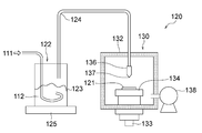
- FIG. 3 is a schematic cross-sectional view showing an AD film forming apparatus used in Examples 1 and 2.
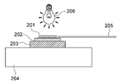
- FIG. 3 is a schematic cross-sectional view showing a heating device used in Examples 1 and 2.
- FIG. 3 is a schematic cross-sectional view showing a heating device used in Examples 1 and 2.
- FIG. 1 shows an example of a surface light emitting element according to the present invention.
- the surface light emitting device 10 shown in FIG. 1 includes a substrate 12, a light emitting functional layer 14 provided on the substrate, and an electrode 16 provided on the light emitting functional layer. If desired, the surface light emitting device 10 may further include a phosphor layer 17 and / or a reflective layer 18 outside the electrode 16.
- the light emitting functional layer 14 is composed of a p-type zinc oxide layer so as to constitute a part of a light emitting element utilizing a pn junction, while the substrate 12 is composed of an n-type zinc oxide single crystal.
- the structure can function as an n-type zinc oxide layer.
- the surface emitting element 10 of the example of illustration becomes a structure by which the n-type zinc oxide layer was abbreviate
- the substrate 12 is composed of a zinc oxide single crystal having a thickness of 100 ⁇ m or more, preferably a conductive zinc oxide single crystal.
- the zinc oxide single crystal has a hexagonal wurtzite structure, may contain a dopant as another element, and is preferably a conductive zinc oxide single crystal.
- the zinc oxide single crystal may be made of ZnO mixed with one or more kinds of crystals selected from the group consisting of MgO, CdO, ZnS, ZnSe, and ZnTe. That is, even if mixed crystals are used, any zinc oxide-based single crystal having a hexagonal wurtzite structure is included in the zinc oxide single crystal of the present invention.
- the zinc oxide single crystal is doped with an n-type dopant regardless of whether it is mixed or not, so that the substrate 12 can be configured to function as an n-type zinc oxide layer.
- the n-type dopant include aluminum (Al), gallium (Ga), indium (In), boron (B), fluorine (F), chlorine (Cl), bromine (Br), iodine (I) and silicon. 1 or more types selected from the group which consists of (Si) are mentioned.
- Such a zinc oxide single crystal can have various advantageous properties such as conductivity, crystallinity, and transparency, and by using this as a substrate, a high-performance surface light emitting device can be provided at low cost.
- the present inventors use a technique such as a solid phase epitaxial growth method or a hydrothermal method to produce a low-resistance zinc oxide single crystal of preferably 1 ⁇ 10 ⁇ 3 ⁇ cm or less at a thickness of 100 ⁇ m or more at low cost. The knowledge that it can produce is obtained.
- the zinc oxide single crystal having such a thickness is suitable for increasing the area from the viewpoint of cost and mechanical strength, and not only enables inexpensive production of a large area surface light emitting device, but also has conductivity and crystal By adopting a configuration that maximizes the use of various advantageous characteristics such as property and transparency, a high-performance surface light emitting device can be realized.
- the constituent layer of the light emitting functional layer 14 is formed on the zinc oxide single crystal substrate 12 by epitaxial growth, so that high light emission efficiency can be obtained. Further, by using the zinc oxide single crystal substrate, the crystallinity of the light emitting functional layer 14 is increased and the light emission efficiency is improved. In particular, when a zinc oxide single crystal substrate to which an n-type dopant is added is used, diffusion of the n-type dopant into the substrate, which becomes a problem when an n-type layer is formed on an undoped zinc oxide substrate, can be suppressed. The quality of the surface light emitting element can be stabilized.
- n-type zinc oxide single crystal that has been remarkably reduced in resistance by adding an n-type dopant
- the substrate 12 not only the n-type layer but also the n-type layer side is opposed to the substrate 12 itself as in the illustrated example.
- a function as an electrode can be provided, and the configuration can be simplified by eliminating the n-type layer and / or the counter electrode on the n-type layer side.
- heat generation at the time of light emission is suppressed by reducing the resistance of the substrate 12 functioning as an n-type layer, and the light emission efficiency can be further increased.
- the counter electrode on the back surface side of the substrate 12 is not required, light can be extracted from the back surface of the substrate 12 due to the transparency of the zinc oxide single crystal, and more preferably, only visible light is extracted. It is also possible to.
- the light emitting functional layer 14 can emit ultraviolet light
- a phosphor layer 17 for converting ultraviolet light to visible light is provided outside the electrode 16, and It is preferable that the reflection layer 18 be provided outside the phosphor layer 17 so that only visible light not including ultraviolet light is extracted. That is, according to this configuration, the ultraviolet light from the light emitting functional layer 14 is converted into visible light by the phosphor layer 17, while the unconverted ultraviolet light is absorbed by the zinc oxide single crystal zinc oxide single crystal 12, As a result, only visible light can be extracted from the back side of the substrate 12 with high efficiency. By doing so, it is possible to realize a white surface light emitting element that does not emit ultraviolet light harmful to the human body.
- the reflective layer 18 may be eliminated and the entire surface light emitting element 10 may emit light.
- the band gap energy of the zinc oxide single crystal is preferably smaller than the energy of ultraviolet light emitted from the light emitting functional layer.
- a surface-emitting element having a large area can be manufactured by using a zinc oxide single crystal having a thickness of 100 ⁇ m or more.
- the preferable thickness of the zinc oxide single crystal substrate 12 is 100 ⁇ m or more, more preferably 300 ⁇ m or more, and more preferably 500 ⁇ m or more.
- substrate 12 has an area of 20 cm ⁇ 2 > or more, More preferably, it is 45 cm ⁇ 2 > or more.
- the substrate 12 preferably has a size of ⁇ 5.08 cm or more, more preferably ⁇ 7.62 cm or more.
- the light emitting functional layer 14 is provided on the substrate.
- the light emitting functional layer 14 may be any layer that has a light emitting function in the light emitting element, and the type and method of the light emitting element are not limited as long as a desired light emitting function can be secured on the zinc oxide single crystal that is a constituent material of the substrate 12. . Therefore, the light emitting functional layer 12 may emit blue or red visible light, or may emit ultraviolet light without visible light or together with visible light. In this regard, since the light emitting functional layer 14 shown in FIG. 1 is configured to emit ultraviolet light, a phosphor layer 17 is separately provided to convert the ultraviolet light into visible light.
- the light-emitting functional layer 14 preferably constitutes at least a part of a light-emitting element using a pn junction, and the pn junction may include a light-emitting layer between the p-type layer and the n-type layer. . Further, as one form of the p-type layer-the light-emitting layer-the n-type layer, a quantum well structure in which the light-emitting layer is thin can be adopted. In the case of a pn junction, each of the p-type layer, the n-type layer, and the light-emitting layer (when the light-emitting layer is included) can be made of a zinc oxide-based material, which is also made of zinc oxide. Therefore, it is easy to align the orientation or crystal orientation with the substrate, thereby increasing the light emission efficiency.
- the light emitting functional layer 14 preferably includes at least a p-type zinc oxide layer made of ZnO doped with a p-type dopant.
- the substrate 12 is configured to function as an n-type zinc oxide layer.
- a light-emitting element having a ⁇ n junction can be configured.
- a light emitting element having a pn junction can be formed by a combination thereof.
- Preferred examples of the p-type dopant include nitrogen (N), phosphorus (P), arsenic (As), carbon (C), lithium (Li), sodium (Na), potassium (K), silver (Ag), and copper. 1 or more types selected from the group which consists of (Cu) are mentioned.
- the p-type zinc oxide layer may be made of ZnO mixed with one or more kinds of crystals selected from the group consisting of MgO, CdO, ZnS, ZnSe, and ZnTe. ZnO may be doped with a p-type dopant.
- a compound in which Mg x Zn 1-x O (0.1 ⁇ x ⁇ 0.4), which is a mixed crystal of ZnO and MgO, is doped with N is particularly preferable.
- ZnO mixed with MgO the band gap is widened, and the emission wavelength can be shifted to a higher energy side.
- ZnO may be a mixed crystal with CdO or ZnS, whereby the band gap is narrowed, and the emission wavelength can be shifted to the low energy side.
- the preparation of the p-type zinc oxide layer can be preferably performed by a solid phase epitaxial growth method using a commercially available p-type ZnO powder or an RS-MBE method (radical source molecular beam growth), but is not limited thereto. It can also be carried out by a technique of applying p-type zinc oxide by a MOCVD method or a solution method such as spin coating or dipping and heat-treating at 300 to 700 ° C.
- the light emitting functional layer 14 may further include an n-type zinc oxide layer doped with an n-type dopant between the p-type zinc oxide layer and the substrate 12.
- the n-type dopant include aluminum (Al), gallium (Ga), indium (In), boron (B) fluorine (F), chlorine (Cl), bromine (Br), iodine (I) and silicon ( 1 or more types selected from the group consisting of Si).
- the n-type zinc oxide layer may be made of ZnO mixed with one or more kinds of crystals selected from the group consisting of MgO, CdO, ZnS, ZnSe, and ZnTe. ZnO may be doped with an n-type dopant.
- a compound in which Mg x Zn 1-x O (0.1 ⁇ x ⁇ 0.4), which is a mixed crystal of ZnO and MgO, is doped with Al or Ga is particularly preferable.
- the n-type zinc oxide layer can be omitted.
- the light-emitting functional layer 14 includes ZnO having a smaller band gap than the p-type zinc oxide layer and the n-type zinc oxide layer, or MgO, CdO, ZnS, between the p-type zinc oxide layer and the n-type zinc oxide layer.
- You may have at least the light emitting layer which consists of a mixed crystal of 1 or more types selected from the group which consists of ZnSe and ZnTe, and does not contain a p-type dopant and an n-type dopant.
- the structure in which the light emitting layer is thin corresponds to a light emitting element having a quantum well structure which is an embodiment of a pn junction, and the light emission efficiency can be further improved.
- the light emitting functional layer is a p-type zinc oxide layer between the p-type zinc oxide layer and the n-type zinc oxide substrate 12.
- ZnO having a smaller band gap than any of the single crystals of zinc oxide, or a mixed crystal of ZnO with one or more selected from the group consisting of MgO, CdO, ZnS, ZnSe, and ZnTe, and a p-type dopant and What is necessary is just to comprise so that it may have at least the light emitting layer which does not contain an n-type dopant.
- the light emitting functional layer 14 is epitaxially grown following the crystal structure of the zinc oxide single crystal, thereby having the same crystal structure as the single crystal substrate. In this way, excellent light emission characteristics can be obtained.
- the method for forming the light emitting functional layer 14 having such a structure is not particularly limited as long as it is a method for promoting growth according to the orientation of the substrate, but sputtering, molecular beam epitaxy (MBE), solid epitaxial growth, etc. Is preferably exemplified.
- the solid epitaxial growth method can be preferably performed, for example, by forming a film on a substrate by an aerosol deposition method (AD method) and making the coating into a single crystal by unidirectional heating from the substrate side.
- AD method aerosol deposition method
- the phosphor layer 17 for converting the ultraviolet light into visible light is further provided outside the electrode 16.
- the phosphor layer 17 is not particularly limited as long as it includes a known fluorescent component capable of converting ultraviolet light into visible light.
- a fluorescent component that emits blue light when excited by ultraviolet light, a fluorescent component that emits blue to green light when excited by ultraviolet light, and a fluorescent component that emits red light when excited by ultraviolet light are mixed. It is preferable that white light is obtained as a mixed color.
- Preferred combinations of such fluorescent components include (Ca, Sr) 5 (PO 4 ) 3 Cl: Eu, BaMgAl 10 O 17 : Eu, and Mn, Y 2 O 3 S: Eu, and these components Is preferably dispersed in a resin such as a silicone resin to form the phosphor layer 17.
- a fluorescent component is not limited to the above-exemplified substances, and may be a combination of other ultraviolet light-excited phosphors such as yttrium aluminum garnet (YAG), silicate phosphors, and oxynitride phosphors. .
- a phosphor layer 17 for converting blue light into yellow light is further provided outside the electrode 16.
- the phosphor layer 17 is not particularly limited as long as it includes a known fluorescent component capable of converting blue light into yellow light. For example, it may be combined with a phosphor emitting yellow light such as YAG. By doing in this way, since blue light emission which permeate
- the phosphor layer 17 includes both a fluorescent component for converting blue to yellow and a fluorescent component for converting ultraviolet light to visible light, thereby converting ultraviolet light into visible light and blue light. It is good also as a structure which performs both conversion to yellow light.
- the electrode 16 is provided on the light emitting functional layer 14.
- the electrode 16 may be formed of a known electrode material. However, when light is converted by the phosphor layer 17 and / or when light is extracted from the electrode 16 side, a transparent conductive film such as ITO, or A metal electrode having a high aperture ratio such as a lattice structure or a moth-eye structure is preferable in terms of increasing the conversion and / or extraction efficiency of light generated in the light emitting functional layer 14.
- the reflective layer 18 may be further provided outside the phosphor layer 17.
- the material and thickness of the reflective layer 18 are not particularly limited as long as they can reflect visible light from the phosphor, and may be made of a highly reflective metal such as Au or Al.
- the substrate 12 is configured to function as a counter electrode.
- a counter electrode may be separately provided on the side of the substrate 12 opposite to the light emitting functional layer 14.
- the counter electrode may be made of a known electrode material.
- the aperture ratio of a transparent conductive film such as ITO, or a lattice structure or a moth-eye structure is high.
- a metal electrode is preferable in that the extraction efficiency of light generated in the light emitting functional layer 14 can be increased.
- the n-type layer included in the light emitting functional layer 14 may be used as an electrode, or an electrode may be provided on the n-type layer.
- the zinc oxide single crystal used as the substrate 12 may be produced by any method, but a highly doped conductive zinc oxide single crystal suitable as the substrate 12 is produced by the method described below. It can manufacture preferably.
- the manufacturing method of a highly doped electroconductive zinc oxide single crystal is not restricted to the following method, For example, you may use the hydrothermal synthesis method and the liquid phase epitaxial method (LPE method).
- raw material powder As a raw material powder for producing a conductive zinc oxide single crystal, a zinc oxide raw material powder to which a dopant is dissolved or added is produced.
- This doped raw material powder may be produced by any method regardless of the solid phase method or the liquid phase method.
- the production of the zinc oxide raw material powder by the solid phase method can be preferably carried out by mixing non-doped zinc oxide particles and particles of a compound such as an oxide of a dopant element with a pot mill, a ball mill or the like, followed by heat treatment.
- This heat treatment may be performed under conditions suitable for a solid phase reaction, and is preferably performed at 900 to 1500 ° C. for 1 to 5 hours, more preferably at 1000 to 1400 ° C. for 1 to 5 hours.
- the heat-treated powder is preferably pulverized to a desired average particle size by pot milling, ball milling or the like.
- the preferred volume-based D50 average particle diameter of the raw material powder after pulverization is 0.2 to 4 ⁇ m.
- the zinc oxide raw material powder is sprayed to form a film mainly composed of zinc oxide on a seed substrate containing the zinc oxide single crystal, and the formed film remains in a solid state. Crystallization produces a zinc oxide single crystal.
- the spray film formation method include an aerosol deposition method (AD method) and a powder jet deposition method (PJD method).
- the film forming method is not limited to the method using the above-described powder injection, and any method selected from the group consisting of a physical vapor deposition (PVD) method and a chemical vapor deposition (CVD) method may be used.
- Specific examples of the physical vapor deposition (PVD) method include a sputtering method.
- examples of the chemical vapor deposition (CVD) method include a mist CVD method and a laser CVD method.
- the step of crystallizing the formed film in a solid state is performed by using an infrared lamp (for example, a near infrared lamp), various lasers (for example, a CO 2 laser, a YAG laser, an excimer laser, a semiconductor laser, etc.) as a heat source. It is desirable to use a method that uses heat treatment such as light heating or a high-frequency heating device.
- the heating step is performed after the film formation.
- a method of spraying the zinc oxide raw material powder while heating the substrate at a temperature at which the zinc oxide single crystal can be grown may be used.
- the heating temperature is more preferably 900 ° C. or higher, and further preferably 1000 to 1400 ° C.
- Example 1 As shown in FIG. 1, a light emitting functional layer 14 using a pn junction, an electrode 16, a phosphor layer 17, and a reflective layer 18 are formed in this order on an n-type ZnO single crystal substrate 12 in order.
- n-type ZnO single crystal substrate 12 were made and evaluated. Specifically, it is as follows.
- the following examples are examples using the board
- the solid phase epitaxial growth method is used for manufacturing the n-type ZnO single crystal substrate, other methods such as a hydrothermal method and LPE may be used.
- n-type ZnO single crystal substrate 1a
- zinc oxide (ZnO) in which aluminum (Al) was dissolved was prepared as follows. First, zinc oxide (ZnO) powder (volume-based median diameter (D50): 0.8 ⁇ m) and aluminum oxide (Al 2 O 3 ) powder (volume-based D50: 0.5 ⁇ m) are converted into atomic moles of aluminum (Al). They were weighed and mixed so that the ratio was 0.2 at%. The obtained mixed powder was wet-mixed in a pot mill. This wet-mixed powder was fired at 1400 ° C.
- zinc oxide (ZnO) powder in which aluminum (Al) was dissolved.
- the obtained synthetic powder was wet-ground for 5 hours in a pot mill using zirconia balls so that the volume standard D50 was 2.6 ⁇ m.
- zinc oxide (ZnO) in which 0.2 at% of aluminum (Al) was dissolved was obtained as a film forming raw material powder.
- the raw material powder for film formation obtained in (1a) above was deposited on a commercially available ZnO single crystal substrate (diameter: 7.62 cm, thickness: 0.5 mm, c-plane) by an aerosol deposition method (hereinafter referred to as “a”). , Referred to as AD).
- a film forming apparatus 120 shown in FIG. 2 was used for AD film formation.
- the film forming apparatus 120 includes an aerosol generating unit 122 that generates an aerosol of a raw material powder containing a raw material component, and a film forming unit 130 that sprays the film forming powder onto the seed substrate 121 to form a film containing the raw material component. ing.
- the aerosol generating unit 122 contains the film forming powder 112 and receives the supply of the carrier gas 111 from a gas cylinder (not shown) to generate an aerosol, and supplies the generated aerosol to the film forming unit 130.
- a raw material supply pipe 124, an aerosol generation chamber 123, and a vibrator 125 for applying vibration to the aerosol therein at a frequency of 10 to 100 Hz are provided.
- the film forming unit 130 includes a film forming chamber 132 for injecting aerosol onto the seed substrate 121, a seed substrate holder 134 that is disposed inside the film forming chamber 132 and fixes the seed substrate 121, and the seed substrate holder 134 is X-axis- And an XY stage 133 that moves in the Y-axis direction.
- the film forming unit 130 includes a spray nozzle 136 that has a slit 137 formed at the tip thereof and sprays aerosol onto the seed substrate 121, and a vacuum pump 138 that decompresses the film forming
- the film forming apparatus 120 nitrogen (N 2 ) gas is allowed to flow as a carrier gas 111 at a flow rate of 6 L / min, the pressure in the aerosol generation chamber 123 is 50 to 70 kPa, and the pressure in the film forming chamber 132 is 0.1 kPa.
- the opening size of the slit 137 provided in the film-forming powder injection nozzle 136 was set to 10 mm ⁇ 0.8 mm.
- the scanning distance of one scan is 80 mm
- the scanning speed is 1 mm / second
- the film is formed by shifting the 10 mm scanning position after the end of one scan, and a total of eight rows are scanned in one cycle. went. This film formation was performed for a total of 60 cycles to obtain an AD film made of Al-doped ZnO having a thickness of about 2.5 ⁇ m.
- the seed substrate 202 and the platinum plate 203 were placed on a quartz pedestal 204, and the temperature of the film 201 was measured by a thermocouple 205.
- the heat treatment was performed in the air, heated at a temperature rising rate of 400 ° C./min, and held at 1250 ° C. for 10 minutes.
- the ZnO film was subjected to solid phase epitaxial growth that grew following the surface atomic arrangement of the single crystal serving as the substrate, and became an Al-doped ZnO (hereinafter referred to as AZO) single crystal film.
- AZO Al-doped ZnO
- the confirmation of single crystallization was carried out by measuring the in-plane rocking curve (XRC) using a multifunctional high resolution X-ray diffractometer (D8 DISCOVER, manufactured by Bruker AXS Co., Ltd.) under the following conditions. Since a (100) peak was detected, it was judged that a single crystal film was obtained satisfactorily.
- XRC measurement conditions > ⁇ Tube voltage: 40kV ⁇ Tube current: 40 mA ⁇ Anti-scattering slit: 3 ° ⁇ Step width: 0.001 ° ⁇ Scanning speed: 0.5 seconds / step ⁇ Incident angle: 1 °
- a p-type ZnO layer 14 made of N-doped p-type ZnO (hereinafter referred to as ZnO: N) is formed.
- the solid phase epitaxial growth was used as follows. First, a commercially available N-doped p-type ZnO powder (hereinafter referred to as ZnO: N powder) is formed on an n-type ZnO single crystal substrate by using an AD apparatus shown in FIG. A dense ZnO: N film was obtained.
- N 2 nitrogen
- the pressure in the aerosol generation chamber 123 is 50 kPa
- the pressure in the film formation chamber 132 is 0.1 kPa or less
- film formation is performed.
- the opening size of the slit 137 provided in the powder injection nozzle 136 was 10 mm ⁇ 0.4 mm.
- the scanning distance of one scan is 80 mm
- the scanning speed is 1 mm / second
- the film is formed by shifting the 10 mm scanning position after the end of one scan, and a total of eight rows are scanned in one cycle. went.
- This film formation was performed for a total of 60 cycles to obtain an AD film made of ZnO: N having a thickness of about 2.5 ⁇ m.
- the film forming method is the AD method, but a PJD method, a sputtering method, a laser CVD method, a mist CVD method, a spin coating method, a dipping method, or the like may be used.
- single crystallization was performed using the infrared lamp heating apparatus of FIG. The heat treatment was performed in nitrogen, heated at a heating rate of 400 ° C./min, and held at 1100 ° C. for 10 minutes.
- the ZnO: N film was subjected to solid phase epitaxial growth that grew in accordance with the crystal structure of the n-type ZnO single crystal substrate, and a ZnO: N single crystal film was obtained.
- a ZnO: N single crystal film was obtained.
- the n-type ZnO single crystal film and the ZnO: N single crystal film were energized and subjected to IV measurement, rectification was confirmed, and the ZnO: N single crystal film functioned as a p-type ZnO layer. It was confirmed that a good pn junction was formed by the heat treatment.
- Electrode layer on the p-type ZnO layer 14, 30 nm of Au was formed by electron beam evaporation to obtain an electrode 16.
- the electrode in this example is an Au thin film, an electrode having a high aperture ratio such as a lattice shape or a transparent conductive film such as ITO may be used for the Au portion in order to increase luminous efficiency.
- n-type ZnO single crystal substrate In order to increase the efficiency as a surface light source, the light emission from the light emitting functional layer 14 side is suppressed by the reflective layer 18 and the light emission intensity from the back surface side of the substrate 12 is amplified.
- the reflective layer 18 may be eliminated and the entire surface light emitting device 10 may emit light.
- Example 2 A surface-emitting device was prepared and evaluated in the same manner as in Example 1 except that the p-type ZnO layer was prepared by RS-MBE (radical source molecular beam growth).
- the p-type ZnO layer was produced on the n-type ZnO single crystal substrate obtained in (1c) of Example 1 using an RS-MBE (radical source molecular beam growth) apparatus.
- zinc (Zn) which is a metal material
- Zn zinc
- Oxygen (O) and nitrogen (N) which are gas materials, are expressed as oxygen radicals (O *) and nitrogen radicals (N *) using O 2 gas and NO gas as raw materials in an RF radical generator, respectively.
- the purity of various raw materials was 7N for Zn, 6N for O 2 , and 5N for NO gas.
- the substrate was heated to 700 ° C.
- Example 2 (2) the n-type ZnO single crystal film and the ZnO: N single crystal film were energized and subjected to IV measurement. As a result, rectification was confirmed, and the ZnO: N single crystal film was p. It was confirmed that it functions as a type ZnO layer and that a high-quality pn junction is formed by heat treatment.
- the surface light emitting device 10 was obtained by sequentially forming the electrode 16, the phosphor layer 17, and the reflective layer 18 on the p-type ZnO layer 14 obtained in the same manner as in Example 1.
- the obtained surface light emitting device when current was passed between the electrode 16 and the n-type ZnO single crystal substrate 12, only white light emission was observed from the entire area of the n-type ZnO single crystal substrate 12, and no ultraviolet light was detected. .
- the phosphor layer 17 was removed and the emission wavelength was measured from the light emitting functional layer side, an ultraviolet emission of about 375 nm was observed, and the ultraviolet emission from the pn junction was converted into visible light by the phosphor layer 17. It was confirmed that the unconverted ultraviolet light was absorbed by the ZnO single crystal substrate 12.
- n-type ZnO single crystal substrate since a low-resistance n-type ZnO single crystal substrate was used, it was found that there was almost no heat generation during light emission and high efficiency. From these results, by using a low-resistance n-type ZnO single crystal substrate, a lower (n-type side) electrode is unnecessary, and a white light emitting element having a vertical structure can be manufactured.
- the light emission from the light emitting functional layer 14 side is suppressed by the reflective layer 18 and the light emission intensity from the back surface side of the substrate 12 is amplified.
- the reflective layer 18 may be eliminated and the entire surface light emitting device 10 may emit light.
Landscapes
- Led Devices (AREA)
- Crystals, And After-Treatments Of Crystals (AREA)
Abstract
100μm以上の厚さを有する酸化亜鉛単結晶から構成される基板と、紫外光を放出可能な発光機能層と、発光機能層上に設けられる電極と、電極の外側に設けられる、紫外光を可視光に変換するための蛍光体層と、蛍光体層の外側に設けられる反射層とを備えた、面発光素子が提供される。本発明によれば、高性能な面発光素子を安価に提供することができる。
Description
本発明は、酸化亜鉛基板を用いた面発光素子に関する。
近年、次世代照明として面発光EL照明が注目されている。面発光EL照明には、明るさの均一性が高い、薄型で省スペースである、デザイン性が高い、目に優しいといった利点がある。面発光EL照明は、有機ELを用いたものでは一部製品化されているが、コスト及び耐久性の面で全面的な普及への課題は依然として多い。また、発光ダイオード(LED)を用いる場合は、高価な基板を使用する必要があるため、素子の大面積化が難しいという問題がある。
一方、酸化亜鉛(ZnO)は、安全、安価であり、化学的にも安定で、透明性にも優れた材料として知られており、その広いバンドギャップや優れた光学特性から、発光ダイオード(LED)等の発光素子への応用が期待されている。例えば非特許文献1には、Zn極性ZnO単結晶基板上にNをドープしたMgxZn1-xO膜を形成して作製したLEDにおいて紫外発光を観測したことが報告されている。
このような発光素子に用いられる酸化亜鉛単結晶基板には、導電性及び結晶性の両方が高いことが求められる。このため、導電性を向上させる異種元素(以下、ドーパントという)を酸化亜鉛単結晶にドーピングすることが一般的に行われる。例えば、特許文献1(特開2004-315361号公報)には、導電性向上のためにAlやFe等をドープした酸化亜鉛単結晶を水熱合成法により製造することが開示されている。また、特許文献2(国際公開第2007/100146号)には、液相成長法による酸化亜鉛単結晶の製造において各種のドーパントを添加可能であることが開示されている。
K. Nakahara et al., "Nitrogendoped MgxZn1−xO/ZnO single heterostructure ultraviolet light-emitting diodes onZnO substrates", Applied Physics Letters 97, 013501 (2010)
本発明者らは、今般、100μm以上の厚さを有する酸化亜鉛単結晶を基板として用いることで、高性能な面発光素子を安価に提供できるとの知見を得た。
したがって、本発明の目的は、高性能な面発光素子を安価に提供することにある。
本発明の一態様によれば、100μm以上の厚さを有する酸化亜鉛単結晶から構成される基板と、
前記基板上に設けられる、紫外光を放出可能な発光機能層と、
前記発光機能層上に設けられる電極と、
前記電極の外側に設けられる、前記紫外光を可視光に変換するための蛍光体層と、
前記蛍光体層の外側に設けられる反射層と、
を備えた、面発光素子が提供される。
前記基板上に設けられる、紫外光を放出可能な発光機能層と、
前記発光機能層上に設けられる電極と、
前記電極の外側に設けられる、前記紫外光を可視光に変換するための蛍光体層と、
前記蛍光体層の外側に設けられる反射層と、
を備えた、面発光素子が提供される。
本発明の別の一態様によれば、100μm以上の厚さを有する導電性酸化亜鉛単結晶から構成される基板と、
前記基板上に設けられる発光機能層と、
前記発光機能層上に設けられる電極と、
を備えた、面発光素子が提供される。
前記基板上に設けられる発光機能層と、
前記発光機能層上に設けられる電極と、
を備えた、面発光素子が提供される。
面発光素子
図1に、本発明による面発光素子の一例を示す。図1に示される面発光素子10は、基板12と、基板上に設けられる発光機能層14と、発光機能層上に設けられる電極16とを備えてなる。所望により、面発光素子10は、電極16の外側に蛍光体層17及び/又は反射層18を更に備えてもよい。なお、図1において、発光機能層14はp-n接合を利用した発光素子の一部を構成すべくp型酸化亜鉛層で構成される一方、基板12はn型酸化亜鉛単結晶で構成されてn型酸化亜鉛層として機能しうる構成となっている。このため、図示例の面発光素子10はn型酸化亜鉛層が省略された構成となっているが、本発明はこれに限定されない。
図1に、本発明による面発光素子の一例を示す。図1に示される面発光素子10は、基板12と、基板上に設けられる発光機能層14と、発光機能層上に設けられる電極16とを備えてなる。所望により、面発光素子10は、電極16の外側に蛍光体層17及び/又は反射層18を更に備えてもよい。なお、図1において、発光機能層14はp-n接合を利用した発光素子の一部を構成すべくp型酸化亜鉛層で構成される一方、基板12はn型酸化亜鉛単結晶で構成されてn型酸化亜鉛層として機能しうる構成となっている。このため、図示例の面発光素子10はn型酸化亜鉛層が省略された構成となっているが、本発明はこれに限定されない。
基板12は100μm以上の厚さを有する酸化亜鉛単結晶、好ましくは導電性酸化亜鉛単結晶から構成される。酸化亜鉛単結晶は六方晶ウルツ鉱型構造を有しており、他の元素としてドーパントを含んでいてもよく、それにより導電性酸化亜鉛単結晶とされているのが好ましい。また、酸化亜鉛単結晶は、MgO、CdO、ZnS、ZnSe及びZnTeからなる群から選択される1種以上の結晶と混晶化されたZnOからなるものであってもよい。すなわち、混晶化されていても、六方晶ウルツ鉱型構造を有する酸化亜鉛ベースの単結晶であれば、本発明における酸化亜鉛単結晶に包含される。また、混晶化されているか否かを問わず、酸化亜鉛単結晶にはn型ドーパントがドープされるのが好ましく、それにより基板12がn型酸化亜鉛層として機能するように構成されてもよい。n型ドーパントの好ましい例としては、アルミニウム(Al)、ガリウム(Ga)、インジウム(In)、硼素(B)、フッ素(F)、塩素(Cl)、臭素(Br)、ヨウ素(I)及びシリコン(Si)からなる群から選択される1種以上が挙げられる。
このような酸化亜鉛単結晶は、導電性、結晶性、透明性等の様々な有利な特性を有することができ、これを基板として用いることで、高性能な面発光素子を安価に提供することができる。特に、本発明者らは、固相エピタキシャル成長法や水熱法等の手法を用いることで、望ましくは1×10⁻³Ωcm以下という低抵抗な酸化亜鉛単結晶を100μm以上の厚さで安価に作製できるとの知見を得ている。そして、このような厚みの酸化亜鉛単結晶はコスト及び機械強度の観点から大面積化に適し、大面積面発光素子の安価な製造を可能にするのみならず、それが持ちうる導電性、結晶性、透明性等の種々の有利な特性を最大限に活用する構成を採用することで高性能の面発光素子を実現することができる。
例えば、酸化亜鉛単結晶基板12上に発光機能層14の構成層をエピタキシャル成長により形成した場合、単結晶基板と同一の結晶構造が実現可能となるため、高い発光効率を得ることができる。また、酸化亜鉛単結晶基板を用いることで発光機能層14の結晶性が高まって発光効率が向上する。特にn型ドーパントの添加した酸化亜鉛単結晶基板を用いた場合、ドーピングされていない酸化亜鉛基板上にn型層を形成したときに問題となる、n型ドーパントの基板への拡散も抑制でき、面発光素子の品質を安定化できる。また、n型ドーパントを添加して著しく低抵抗化したn型酸化亜鉛単結晶を基板12として用いる場合には、図示例のように基板12自体にn型層だけでなくn型層側の対向電極としての機能を持たせることができ、n型層及び/又はn型層側の対向電極を不要にして構成を簡素化できる。また、n型層として機能する基板12の低抵抗化によって発光時の発熱が抑制され、発光効率を更に高めることができる。その上、基板12の裏面側の対向電極を不要とした場合には、酸化亜鉛単結晶の透明性によって、基板12裏面から光を取り出すことが可能であり、より好ましくは可視光のみを取り出す構成とすることも可能となる。
例えば、発光機能層14が紫外光を放出可能な場合には、図1に示されるように、電極16の外側に、紫外光を可視光に変換するための蛍光体層17を設け、且つ、蛍光体層17の外側に反射層18を設けることで、紫外光を含まない可視光のみを取り出すように構成するのが好ましい。すなわち、この構成によれば、発光機能層14からの紫外光が蛍光体層17によって可視光に変換される一方、変換されなかった紫外光が酸化亜鉛単結晶酸化亜鉛単結晶12によって吸収され、その結果、可視光のみが基板12の裏面側から高効率に取り出されることが可能となる。こうすることで、人体に有害な紫外光を発しない白色面発光素子を実現できる。その上、反射層18によって電極16側からの光放出を抑制し、基板12裏面側からの発光強度を増幅する構成となるため、面光源としての発光効率を有意に高めることができる。もっとも、用途によっては反射層18を無くして面発光素子10全体を発光させる構成としてもよい。なお、酸化亜鉛単結晶のバンドギャップエネルギーは、発光機能層から発せられた紫外光のエネルギーより小さいことが望ましい。
前述のとおり、100μm以上の厚さを有する酸化亜鉛単結晶を用いることで大面積の面発光素子の製造が可能となる。酸化亜鉛単結晶基板12の好ましい厚さは100μmで以上であり、より好ましくは300μm以上、より好ましくは500μm以上である。また、基板12は20cm2以上の面積を有するのが好ましく、より好ましくは45cm2以上である。別の表現をすれば、基板12はφ5.08cm以上の大きさを有するのが好ましく、より好ましくはφ7.62cm以上である。基板12は大きければ大きいほど面発光素子として面発光照明等への用途が広がる点で好ましく、その面積ないし大きさに上限は規定されるべきではない。
発光機能層14が基板上に設けられる。発光機能層14は、発光素子における発光機能を担う層であればよく、基板12の構成材料である酸化亜鉛単結晶上で所望の発光機能を確保できるかぎり、発光素子の種類や方式は限定されない。従って、発光機能層12は青色、赤色等の可視光を放出するものであってもよいし、可視光を伴わずに又は可視光と共に紫外光を発光するものであってもよい。この点、図1に示される発光機能層14は紫外光を発光するものとして構成されているため、蛍光体層17を別途設けて紫外光を可視光に変換する構成とされている。発光機能層14は、p-n接合を利用した発光素子の少なくとも一部を構成するのが好ましく、このp-n接合はp型層とn型層の間に発光層を含んでいても良い。また、p型層-発光層-n型層の一形態として、発光層の厚みを薄くした量子井戸構造を採りうる。p-n接合の場合にはp型層、n型層及び(発光層を含む場合には)発光層の各層をいずれも酸化亜鉛系の材料で構成することができ、同じく酸化亜鉛で構成される基板との間で配向ないし結晶方位を整合させやすく、それにより発光効率を高めることができる。
発光機能層14は、p型ドーパントがドープされたZnOからなるp型酸化亜鉛層を少なくとも含むのが好ましい。これにより、図1に示されるようにn型酸化亜鉛層を有しない構成の場合には、基板12をn型酸化亜鉛層として機能しうるように構成することで、基板12との組み合わせによりp-n接合による発光素子を構成可能である。一方、n型酸化亜鉛層が存在する場合にはそれとの組み合わせによりp-n接合による発光素子を構成しうる。p型ドーパントの好ましい例としては、窒素(N)、リン(P)、砒素(As)、カーボン(C)、リチウム(Li)、ナトリウム(Na)、カリウム(K)、銀(Ag)及び銅(Cu)からなる群から選択される1種以上が挙げられる。また、p型酸化亜鉛層は、MgO、CdO、ZnS、ZnSe及びZnTeからなる群から選択される1種以上の結晶と混晶化されたZnOからなるものであってもよく、この混晶化されたZnOにp型ドーパントがドープされていてもよい。例えば、ZnOとMgOの混晶であるMgxZn1-xO(0.1≦x≦0.4)にNをドープした化合物が特に好ましい。ZnOをMgOと混晶化することでバンドギャップが広がり、発光波長を高エネルギー側にシフトさせることができる。また、ZnOをCdO又はZnSとの混晶としてもよく、これによりバンドギャップが狭まり、発光波長を低エネルギー側にシフトさせることができる。なお、p型酸化亜鉛層の作製は、市販のp型ZnO粉末を用いた固相エピタキシャル成長法、RS-MBE法(ラジカルソース分子線成長)によって好ましく行うことができるが、これらに限定されず、MOCVD法や、スピンコートやディッピング等の溶液法によってp型酸化亜鉛を塗布し、300~700℃で熱処理する手法によっても行うことができる。
発光機能層14は、p型酸化亜鉛層と基板12との間に、n型ドーパントがドープされたn型酸化亜鉛層を更に備えてもよい。n型ドーパントの好ましい例としては、アルミニウム(Al)、ガリウム(Ga)、インジウム(In)、硼素(B)フッ素(F)、塩素(Cl)、臭素(Br)、ヨウ素(I)及びシリコン(Si)からなる群から選択される1種以上が挙げられる。また、n型酸化亜鉛層は、MgO、CdO、ZnS、ZnSe及びZnTeからなる群から選択される1種以上の結晶と混晶化されたZnOからなるものであってもよく、この混晶化されたZnOにn型ドーパントがドープされていてもよい。例えば、ZnOとMgOの混晶であるMgxZn1-xO(0.1≦x≦0.4)にAl又はGaをドープした化合物が特に好ましい。もっとも、前述したように、基板12がn型酸化亜鉛層として機能するように構成されている場合には、n型酸化亜鉛層は省略可能である。
発光機能層14は、p型酸化亜鉛層とn型酸化亜鉛層との間に、p型酸化亜鉛層及びn型酸化亜鉛層のいずれよりもバンドギャップが小さいZnO、又はMgO、CdO、ZnS、ZnSe及びZnTeからなる群から選択される1種以上とZnOとの混晶からなり、且つ、p型ドーパント及びn型ドーパントを含まない発光層を少なくとも有してもよい。この発光層を薄くした構成はp-n接合の一態様である量子井戸構造の発光素子に相当し、発光効率をより一層高めることができる。もっとも、n型酸化亜鉛層を省略してn型酸化亜鉛基板12を用いる場合には、発光機能層は、p型酸化亜鉛層とn型酸化亜鉛基板12との間に、p型酸化亜鉛層及び酸化亜鉛単結晶のいずれよりもバンドギャップが小さいZnO、又はMgO、CdO、ZnS、ZnSe及びZnTeからなる群から選択される1種以上とZnOとの混晶からなり、且つ、p型ドーパント及びn型ドーパントを含まない発光層を少なくとも有するように構成すればよい。
発光機能層14は、酸化亜鉛単結晶の結晶構造に倣ってエピタキシャル成長し、それにより単結晶基板と同一の結晶構造を有するのが特に好ましい。こうすることで優れた発光特性を得ることができる。このような構造を有する発光機能層14の成膜方法は、基板の配向性に倣った成長を促す方法であれば特に限定されないが、スパッタリング法、分子線エピタキシー法(MBE)、固体エピタキシャル成長法等が好ましく例示される。固体エピタキシャル成長法は、例えば、基板上にエアロゾルデポジション法(AD法)により成膜しておき、被膜を基板側からの一方向加熱により単結晶化することにより好ましく行うことができる。
前述したとおり、発光機能層14が紫外光を放出可能なものである場合には、紫外光を可視光に変換するための蛍光体層17を、電極16の外側に更に備えてなるのが好ましい。蛍光体層17は紫外光を可視光に変換可能な公知の蛍光成分を含む層であればよく特に限定されない。例えば、紫外光により励起されて青色光を発光する蛍光成分、紫外光により励起されて青~緑色光を発光する蛍光成分、及び紫外光により励起されて赤色光を発光する蛍光成分を混在させて、混合色として白色光を得るような構成とするのが好ましい。そのような蛍光成分の好ましい組み合わせとしては、(Ca,Sr)5(PO4)3Cl:Eu、BaMgAl10O17:Eu、及びMn、Y2O3S:Euが挙げられ、これらの成分をシリコーン樹脂等の樹脂中に分散させて蛍光体層17を形成するのが好ましい。このような蛍光成分は上記例示物質に限されるものではなく、他の紫外光励起蛍光体、例えばイットリウム・アルミニウム・ガーネット(YAG)やシリケート系蛍光体、酸窒化物系蛍光体等の組み合わせでもよい。
また、発光機能層14が青色光を放出可能なものである場合には、青色光を黄色光に変換するための蛍光体層17を電極16の外側に更に備えてなるのが好ましい。蛍光体層17は青色光を黄色光に変換可能な公知の蛍光成分を含む層であればよく特に限定されない。例えばYAGなどの黄色発光する蛍光体との組み合わせたものとしてもよい。このようにすることで、蛍光体層を透過した青色発光と蛍光体からの黄色発光は補色関係にあるため、擬似的な白色光源とすることができる。なお、蛍光体層17は、青色を黄色に変換する蛍光成分と、紫外光を可視光に変換するための蛍光成分との両方を備えることで、紫外光の可視光への変換と青色光の黄色光への変換との両方を行う構成としてもよい。
電極16は発光機能層14上に設けられる。電極16は公知の電極材料で構成すればよいが、蛍光体層17で光の変換を行う場合及び/又は電極16側から光を取り出す構成とする場合には、ITO等の透明導電膜、又は格子構造若しくはモスアイ構造等の開口率が高い金属電極とすれば、発光機能層14で発生した光の変換及び/又は取り出し効率を上げられる点で好ましい。
前述したとおり、反射層18が蛍光体層17の外側に更に設けられてもよい。反射層18の材質及び厚さは、蛍光体からの可視光線を反射できるものであれば特に限定されず、AuやAl等の反射性の高い金属で構成すればよい。
図1において基板12は対向電極として機能するように構成されているが、そうでない場合には、基板12の発光機能層14と反対側に対向電極を別途設ければよい。この場合、対向電極は公知の電極材料で構成すればよいが、対向電極側から光を取り出す構成とする場合には、ITO等の透明導電膜、又は格子構造若しくはモスアイ構造等の開口率が高い金属電極とすれば、発光機能層14で発生した光の取り出し効率を上げられる点で好ましい。また、基板12が十分な導電性を持たない場合は発光機能層14中に含まれるn型層を電極としてもよいし、n型層に電極を設置してもよい。
酸化亜鉛単結晶の製造方法
基板12として用いる酸化亜鉛単結晶はいかなる方法によって作製されたものであってもよいが、基板12として適する高ドープの導電性酸化亜鉛単結晶は以下に示される方法により好ましく製造することができる。なお、高ドープの導電性酸化亜鉛単結晶の製法は以下の方法に限るものではなく、例えば水熱合成法や液相エピタキシャル法(LPE法)を用いてもよい。
基板12として用いる酸化亜鉛単結晶はいかなる方法によって作製されたものであってもよいが、基板12として適する高ドープの導電性酸化亜鉛単結晶は以下に示される方法により好ましく製造することができる。なお、高ドープの導電性酸化亜鉛単結晶の製法は以下の方法に限るものではなく、例えば水熱合成法や液相エピタキシャル法(LPE法)を用いてもよい。
(1)原料粉末の作製
導電性酸化亜鉛単結晶の製造用原料粉末として、ドーパントが固溶又は添加された酸化亜鉛原料粉末を作製する。このドープされた原料粉末は、固相法、液相法を問わず、いかなる方法によって製造されたものでもよい。
導電性酸化亜鉛単結晶の製造用原料粉末として、ドーパントが固溶又は添加された酸化亜鉛原料粉末を作製する。このドープされた原料粉末は、固相法、液相法を問わず、いかなる方法によって製造されたものでもよい。
固相法による酸化亜鉛原料粉末の製造は、ノンドープの酸化亜鉛粒子と、ドーパント元素の酸化物等の化合物の粒子とをポットミル、ボールミル等で混合し、熱処理をすることにより好ましく行うことができる。この熱処理は固相反応に適した条件で行えばよく、900~1500℃で1~5時間行われるのが好ましく、より好ましくは1000~1400℃で1~5時間である。熱処理後の粉末はポットミル、ボールミル粉砕等を施して所望の平均粒径に粉砕するのが好ましい。粉砕後の原料粉末の好ましい体積基準D50平均粒径は0.2~4μmである。
(2)酸化亜鉛単結晶の作製
上記酸化亜鉛原料粉末を噴射して、酸化亜鉛単結晶を含む種基板上に主に酸化亜鉛からなる膜を形成すると共に、形成した膜を固相状態のまま結晶化させて酸化亜鉛単結晶を作製する。上記の噴射成膜の手法としては、エアロゾルデポジション法(AD法)及びパウダージェットデポジション法(PJD法)が好ましく挙げられる。また、成膜手法としては上記の粉末の噴射を用いたものに限るものではなく、物理蒸着(PVD)法、及び化学蒸着(CVD)法からなる群より選ばれる何れの方法としてもよい。上記物理蒸着(PVD)法の具体例としては、例えば、スパッタ法等を挙げることができる。更に、化学蒸着(CVD)法としては、例えば、ミストCVD法及びレーザーCVD法等を挙げることができる。
上記酸化亜鉛原料粉末を噴射して、酸化亜鉛単結晶を含む種基板上に主に酸化亜鉛からなる膜を形成すると共に、形成した膜を固相状態のまま結晶化させて酸化亜鉛単結晶を作製する。上記の噴射成膜の手法としては、エアロゾルデポジション法(AD法)及びパウダージェットデポジション法(PJD法)が好ましく挙げられる。また、成膜手法としては上記の粉末の噴射を用いたものに限るものではなく、物理蒸着(PVD)法、及び化学蒸着(CVD)法からなる群より選ばれる何れの方法としてもよい。上記物理蒸着(PVD)法の具体例としては、例えば、スパッタ法等を挙げることができる。更に、化学蒸着(CVD)法としては、例えば、ミストCVD法及びレーザーCVD法等を挙げることができる。
また、形成した膜を固相状態のまま結晶化させる工程は、赤外線ランプ(例えば、近赤外線ランプ等)、各種レーザー(例えば、CO2レーザー、YAGレーザー、エキシマーレーザー、半導体レーザー等)等を熱源とする光加熱や高周波加熱装置等による加熱処理で行う手法が望ましい。尚、上記では成膜後に加熱する工程としたが、酸化亜鉛単結晶が成長可能な温度で基板を加熱しながら酸化亜鉛原料粉末を噴射する方法であっても良い。これらの加熱温度は、より好ましくは900℃以上であり、更に好ましくは1000~1400℃である。
本発明を以下の例によってさらに具体的に説明する。
例1
図1に示されるように、n型ZnO単結晶基板12上に、p-n接合を用いた発光機能層14、電極16、蛍光体層17及び反射層18を順に形成して面発光素子10を作製して、その評価を行った。具体的には以下のとおりである。なお、以下の例はn型ドーパントをAlとした基板を用いる例であるが、Gaドーパント、又はInドーパントなど、他のn型ドーパントを添加した基板でもよい。また、n型ZnO単結晶基板の作製には固相エピタキシャル成長法を用いているが、水熱法やLPE等の他の方法を用いてもよい。
図1に示されるように、n型ZnO単結晶基板12上に、p-n接合を用いた発光機能層14、電極16、蛍光体層17及び反射層18を順に形成して面発光素子10を作製して、その評価を行った。具体的には以下のとおりである。なお、以下の例はn型ドーパントをAlとした基板を用いる例であるが、Gaドーパント、又はInドーパントなど、他のn型ドーパントを添加した基板でもよい。また、n型ZnO単結晶基板の作製には固相エピタキシャル成長法を用いているが、水熱法やLPE等の他の方法を用いてもよい。
(1)n型ZnO単結晶基板の作製
(1a)成膜用原料粉の作製
成膜用原料粉として、アルミニウム(Al)が固溶した酸化亜鉛(ZnO)を以下のようにして調製した。まず、酸化亜鉛(ZnO)粉末(体積基準メジアン径(D50):0.8μm)と酸化アルミニウム(Al2O3)粉末(体積基準D50:0.5μm)とを、アルミニウム(Al)の原子モル比率が0.2at%となるように秤量し、混合した。得られた混合粉末をポットミルにて湿式混合した。この湿式混合した粉末を、大気中、1400℃で5時間に亘って焼成して、アルミニウム(Al)が固溶した酸化亜鉛(ZnO)粉末を合成した。得られた合成粉末を、体積基準D50が2.6μmとなるように、ポットミル中で、ジルコニアボールを用いて、5時間に亘って湿式粉砕した。こうして、アルミニウム(Al)が0.2at%固溶した酸化亜鉛(ZnO)を成膜用原料粉として得た。
(1b)AD膜の作製
上記(1a)で得られた成膜用原料粉を市販のZnO単結晶基板(直径7.62cm、厚さ0.5mm、c面)上にエアロゾルデポジション法(以下、ADという)により堆積させた。AD成膜には図2に示す成膜装置120を使用した。この成膜装置120は、原料成分を含む原料粉末のエアロゾルを生成するエアロゾル生成部122と、成膜粉を種基板121に噴射して原料成分を含む膜を形成する成膜部130とを備えている。
上記(1a)で得られた成膜用原料粉を市販のZnO単結晶基板(直径7.62cm、厚さ0.5mm、c面)上にエアロゾルデポジション法(以下、ADという)により堆積させた。AD成膜には図2に示す成膜装置120を使用した。この成膜装置120は、原料成分を含む原料粉末のエアロゾルを生成するエアロゾル生成部122と、成膜粉を種基板121に噴射して原料成分を含む膜を形成する成膜部130とを備えている。
エアロゾル生成部122は、成膜粉112を収容しガスボンベ(図示せず)からのキャリアガス111の供給を受けてエアロゾルを生成するエアロゾル生成室123と、生成したエアロゾルを成膜部130へ供給する原料供給管124と、エアロゾル生成室123及びその中のエアロゾルに10~100Hzの振動数で振動を付与する加振器125とを備えている。成膜部130は、種基板121にエアロゾルを噴射する成膜チャンバ132と、成膜チャンバ132の内部に配設され種基板121を固定する種基板ホルダ134と、種基板ホルダ134をX軸-Y軸方向に移動するX-Yステージ133とを備えている。また、成膜部130は、先端にスリット137が形成されエアロゾルを種基板121へ噴射する噴射ノズル136と、成膜チャンバ132を減圧する真空ポンプ138とを備えている。
成膜装置120においては、窒素(N2)ガスを6L/分の流量にてキャリアガス111として流し、エアロゾル生成室123の圧力は50~70kPaとし、成膜チャンバ132内の圧力は0.1kPa以下とし、成膜用粉体の噴射ノズル136に備えられたスリット137の開口サイズは10mm×0.8mmとした。成膜時のノズルの走査方法としては、1スキャンの走査距離を80mm、スキャン速度1mm/秒とし、1スキャン終了後、10mm走査位置をずらして成膜を行い、1サイクルで計8列スキャンを行った。この成膜を計60サイクル行い、厚みが約2.5μmのAlドープZnOからなるAD膜を得た。
(1c)AD膜の単結晶化
得られたZnO膜を図3の加熱装置を用いて基板側から一方向加熱した。図3には光加熱のための光源として近赤外線ランプ206を使用した。なお、ZnO膜は近赤外線の吸収係数が低いため、種基板202の膜201が堆積した面とは反対側の面に白金板203を配設し、種基板202の膜201が堆積した面と同じ側から近赤外線を照射して、当該近赤外線を上記白金板203に吸収させることにより、膜201を種基板202側から加熱した。種基板202及び白金板203は石英製台座204上に設置し、熱電対205にて膜201の温度を計測した。加熱処理は大気中で行い、昇温速度400℃/分で加熱し、1250℃で10分間保持した。この熱処理によってZnO膜は基板となる単結晶の表面原子配列に倣って成長する固相エピタキシャル成長を生じ、AlドープされたZnO(以下、AZOという)単結晶膜となった。成膜-熱処理のサイクルを200回繰り返すことで、厚さ500μmのAZO膜を作製した。その後、ワイヤソーにて導電性のないZnO単結晶基板を切断し、AZO単体からなる直径3インチ(7.62cm)の単結晶基板をn型ZnO単結晶基板として得た。
得られたZnO膜を図3の加熱装置を用いて基板側から一方向加熱した。図3には光加熱のための光源として近赤外線ランプ206を使用した。なお、ZnO膜は近赤外線の吸収係数が低いため、種基板202の膜201が堆積した面とは反対側の面に白金板203を配設し、種基板202の膜201が堆積した面と同じ側から近赤外線を照射して、当該近赤外線を上記白金板203に吸収させることにより、膜201を種基板202側から加熱した。種基板202及び白金板203は石英製台座204上に設置し、熱電対205にて膜201の温度を計測した。加熱処理は大気中で行い、昇温速度400℃/分で加熱し、1250℃で10分間保持した。この熱処理によってZnO膜は基板となる単結晶の表面原子配列に倣って成長する固相エピタキシャル成長を生じ、AlドープされたZnO(以下、AZOという)単結晶膜となった。成膜-熱処理のサイクルを200回繰り返すことで、厚さ500μmのAZO膜を作製した。その後、ワイヤソーにて導電性のないZnO単結晶基板を切断し、AZO単体からなる直径3インチ(7.62cm)の単結晶基板をn型ZnO単結晶基板として得た。
単結晶化の確認は多機能高分解能X線回折装置(ブルカー・エイエックスエス株式会社製、D8 DISCOVER)を、以下の条件下で使用して、面内ロッキングカーブ(XRC)測定を行った。(100)ピークが検出されたため、単結晶膜が良好に得られたと判断した。
<XRC測定条件>
・管電圧:40kV
・管電流:40mA
・アンチスキャッタリングスリット:3°
・ステップ幅:0.001°
・スキャンスピード:0.5秒/ステップ
・入射角:1°
<XRC測定条件>
・管電圧:40kV
・管電流:40mA
・アンチスキャッタリングスリット:3°
・ステップ幅:0.001°
・スキャンスピード:0.5秒/ステップ
・入射角:1°
また、抵抗率計(三菱化学株式会社製、ロレスタAX MCP-T370型)を用いて、単結晶体の中心部近傍にて四探針法により体積抵抗率を測定したところ、5×10⁻⁴Ωcmと非常に低抵抗であることが分かった。
(2)固相エピタキシャル成長によるp型ZnO層の成膜
上記得られたn型ZnO単結晶基板12上に、Nドープしたp型ZnO(以下、ZnO:Nという)からなるp型ZnO層14を、固相エピタキシャル成長を用いて以下のようにして作製した。まず、n型ZnO単結晶基板に対し、市販のNドープしたp型ZnO粉末(以下、ZnO:N粉末という)を用いて、図2のAD装置によってn型ZnO層上にAD成膜し、緻密なZnO:N膜を得た。AD成膜は窒素(N2)ガスを10L/分の流量にてキャリアガス111として流し、エアロゾル生成室123の圧力は50kPaとし、成膜チャンバ132内の圧力は0.1kPa以下とし、成膜用粉体の噴射ノズル136に備えられたスリット137の開口サイズは10mm×0.4mmとした。成膜時のノズルの走査方法としては、1スキャンの走査距離を80mm、スキャン速度1mm/秒とし、1スキャン終了後、10mm走査位置をずらして成膜を行い、1サイクルで計8列スキャンを行った。この成膜を計60サイクル行い、厚みが約2.5μmのZnO:NからなるAD膜を得た。なお、本例では成膜方法をAD法としたが、PJD法、スパッタ法、レーザーCVD法、ミストCVD法、スピンコート法、ディッピング法などを用いてもよい。その後、図3の赤外ランプ加熱装置を用いて単結晶化を行った。加熱処理は窒素中で行い、昇温速度400℃/分で加熱し、1100℃で10分間保持した。この熱処理によってZnO:N膜はn型ZnO単結晶基板の結晶構造に倣って成長する固相エピタキシャル成長を生じ、ZnO:N単結晶膜を得た。n型ZnO単結晶膜とZnO:N単結晶膜に通電し、I-V測定を行ったところ、整流性が確認され、ZnO:N単結晶膜がp型ZnO層として機能していること、及び熱処理によって良質なp-n接合が形成されたことが確認できた。
上記得られたn型ZnO単結晶基板12上に、Nドープしたp型ZnO(以下、ZnO:Nという)からなるp型ZnO層14を、固相エピタキシャル成長を用いて以下のようにして作製した。まず、n型ZnO単結晶基板に対し、市販のNドープしたp型ZnO粉末(以下、ZnO:N粉末という)を用いて、図2のAD装置によってn型ZnO層上にAD成膜し、緻密なZnO:N膜を得た。AD成膜は窒素(N2)ガスを10L/分の流量にてキャリアガス111として流し、エアロゾル生成室123の圧力は50kPaとし、成膜チャンバ132内の圧力は0.1kPa以下とし、成膜用粉体の噴射ノズル136に備えられたスリット137の開口サイズは10mm×0.4mmとした。成膜時のノズルの走査方法としては、1スキャンの走査距離を80mm、スキャン速度1mm/秒とし、1スキャン終了後、10mm走査位置をずらして成膜を行い、1サイクルで計8列スキャンを行った。この成膜を計60サイクル行い、厚みが約2.5μmのZnO:NからなるAD膜を得た。なお、本例では成膜方法をAD法としたが、PJD法、スパッタ法、レーザーCVD法、ミストCVD法、スピンコート法、ディッピング法などを用いてもよい。その後、図3の赤外ランプ加熱装置を用いて単結晶化を行った。加熱処理は窒素中で行い、昇温速度400℃/分で加熱し、1100℃で10分間保持した。この熱処理によってZnO:N膜はn型ZnO単結晶基板の結晶構造に倣って成長する固相エピタキシャル成長を生じ、ZnO:N単結晶膜を得た。n型ZnO単結晶膜とZnO:N単結晶膜に通電し、I-V測定を行ったところ、整流性が確認され、ZnO:N単結晶膜がp型ZnO層として機能していること、及び熱処理によって良質なp-n接合が形成されたことが確認できた。
(3)電極層の作製
p型ZnO層14上に、Auを電子ビーム蒸着法にて30nm成膜して電極16を得た。本例の電極はAu薄膜としたが、発光効率を高めるためAu部は格子状など開口率が高い電極やITOなどの透明導電膜を用いてもよい。
p型ZnO層14上に、Auを電子ビーム蒸着法にて30nm成膜して電極16を得た。本例の電極はAu薄膜としたが、発光効率を高めるためAu部は格子状など開口率が高い電極やITOなどの透明導電膜を用いてもよい。
(4)蛍光体層の作製
電極16上に、蛍光体層17を形成すべく、蛍光成分として(Ca,Sr)5(PO4)3Cl:Eu、BaMgAl10O17:Eu,Mn、及びY2O3S:Euを分散含有させたシリコーン樹脂を約5μm塗布した。これらの各蛍光体はそれぞれ紫外光により励起されて青色光、青~緑色光、赤色光を発光し、混合色として白色光を得ることができる。このような蛍光体は上記に挙げたものに限られるものではなく、他の紫外光励起蛍光体、例えばYAGやシリケート系蛍光体、酸窒化物系蛍光体などの組み合わせでも問題はない。
電極16上に、蛍光体層17を形成すべく、蛍光成分として(Ca,Sr)5(PO4)3Cl:Eu、BaMgAl10O17:Eu,Mn、及びY2O3S:Euを分散含有させたシリコーン樹脂を約5μm塗布した。これらの各蛍光体はそれぞれ紫外光により励起されて青色光、青~緑色光、赤色光を発光し、混合色として白色光を得ることができる。このような蛍光体は上記に挙げたものに限られるものではなく、他の紫外光励起蛍光体、例えばYAGやシリケート系蛍光体、酸窒化物系蛍光体などの組み合わせでも問題はない。
(5)反射層の作製
蛍光体層17上に、電極層16と同様、Auを電子ビーム蒸着法にて500nm成膜して反射層18とした。反射層の成分や厚みはこれに限定するものではなく、蛍光体からの可視光線を反射できるものであれば特に限定されない。
蛍光体層17上に、電極層16と同様、Auを電子ビーム蒸着法にて500nm成膜して反射層18とした。反射層の成分や厚みはこれに限定するものではなく、蛍光体からの可視光線を反射できるものであれば特に限定されない。
(6)発光素子の評価
上記のようにして得られた面発光素子において、電極16とn型ZnO単結晶基板12との間に通電したところ、n型ZnO単結晶基板12の全域から白色発光のみが観察され、紫外光は検出されなかった。蛍光体層17を除去して発光機能層側から発光波長を測定したところ、約375nmの紫外発光が観測され、p-n接合部からの紫外発光が蛍光体層17にて可視光に変換されたこと、及び変換されなかった紫外光はZnO単結晶基板12に吸収されたことが確認できた。また、低抵抗なn型ZnO単結晶基板を用いたため、発光時の発熱がほとんど無いことがわかった。これらの結果から、低抵抗なn型ZnO単結晶基板を用いることで、n型層とn型側の電極(対向電極)が不要となり、縦型構造の白色発光素子を作製できた。なお、本例では面光源としての効率を高めるため、反射層18によって発光機能層14側からの光放射を抑制し、基板12裏面側からの発光強度を増幅する構成としたが、用途によっては反射層18を無くして面発光素子10全体を発光させる構成としてもよい。
上記のようにして得られた面発光素子において、電極16とn型ZnO単結晶基板12との間に通電したところ、n型ZnO単結晶基板12の全域から白色発光のみが観察され、紫外光は検出されなかった。蛍光体層17を除去して発光機能層側から発光波長を測定したところ、約375nmの紫外発光が観測され、p-n接合部からの紫外発光が蛍光体層17にて可視光に変換されたこと、及び変換されなかった紫外光はZnO単結晶基板12に吸収されたことが確認できた。また、低抵抗なn型ZnO単結晶基板を用いたため、発光時の発熱がほとんど無いことがわかった。これらの結果から、低抵抗なn型ZnO単結晶基板を用いることで、n型層とn型側の電極(対向電極)が不要となり、縦型構造の白色発光素子を作製できた。なお、本例では面光源としての効率を高めるため、反射層18によって発光機能層14側からの光放射を抑制し、基板12裏面側からの発光強度を増幅する構成としたが、用途によっては反射層18を無くして面発光素子10全体を発光させる構成としてもよい。
例2
p型ZnO層の作製をRS-MBE(ラジカルソース分子線成長)により行ったこと以外は例1と同様にして、面発光素子の作製及び評価を行った。
p型ZnO層の作製をRS-MBE(ラジカルソース分子線成長)により行ったこと以外は例1と同様にして、面発光素子の作製及び評価を行った。
すなわち、p型ZnO層の作製は、例1の(1c)で得られたn型ZnO単結晶基板に対し、RS-MBE(ラジカルソース分子線成長)装置を用いて行った。このとき、金属材料である亜鉛(Zn)はクヌーセンセルで照射し、基板に供給した。ガス材料である酸素(O)と窒素(N)は、RFラジカル発生装置にてそれぞれO2ガス、NOガスを原料とし、酸素ラジカル(O*と表記する)、窒素ラジカル(N*と表記する)として供給した。各種原料の純度はZnが7N、O2が6N、NOガスは5Nのものを用いた。基板は抵抗加熱ヒータを用いて700℃に加熱し、膜中の窒素濃度が1×1020cm-3となるように各種ガスソースのフラックスを制御しながら厚さ100nmのZnO:N単結晶膜を成膜した。例1の(2)と同様に、n型ZnO単結晶膜とZnO:N単結晶膜に通電し、I-V測定を行ったところ、整流性が確認され、ZnO:N単結晶膜がp型ZnO層として機能していること、及び熱処理によって良質なp-n接合が形成されたことが確認できた。
上記得られたp型ZnO層14上に、例1と同様にして、電極16、蛍光体層17及び反射層18を順次形成して、面発光素子10を得た。得られた面発光素子において、電極16とn型ZnO単結晶基板12との間に通電したところ、n型ZnO単結晶基板12の全域から白色発光のみが観察され、紫外光は検出されなかった。蛍光体層17を除去して発光機能層側から発光波長を測定したところ、約375nmの紫外発光が観測され、p-n接合部からの紫外発光が蛍光体層17にて可視光に変換されたこと、及び変換されなかった紫外光はZnO単結晶基板12に吸収されたことが確認できた。また、低抵抗なn型ZnO単結晶基板を用いたため、発光時の発熱がほとんど無く、高効率であることがわかった。これらの結果から、低抵抗なn型ZnO単結晶基板を用いることで、下部(n型側)電極が不要となり、縦型構造の白色発光素子を作製できた。なお、本例では面光源としての効率を高めるため、反射層18によって発光機能層14側からの光放射を抑制し、基板12裏面側からの発光強度を増幅する構成としたが、用途によっては反射層18を無くして面発光素子10全体を発光させる構成としてもよい。
Claims (41)
- 100μm以上の厚さを有する酸化亜鉛単結晶から構成される基板と、
前記基板上に設けられる、紫外光を放出可能な発光機能層と、
前記発光機能層上に設けられる電極と、
前記電極の外側に設けられる、前記紫外光を可視光に変換するための蛍光体層と、
前記蛍光体層の外側に設けられる反射層と、
を備えた、面発光素子。 - 前記発光機能層が、p-n接合に基づいた発光機能を有する、請求項1に記載の面発光素子。
- 前記発光機能層が、前記酸化亜鉛単結晶の結晶方位に倣ってエピタキシャル成長した構造を有し、それにより単結晶基板と同一の結晶構造を有する、請求項1又は2に記載の面発光素子。
- 前記発光機能層が、p型ドーパントがドープされたZnOからなるp型酸化亜鉛層を少なくとも含む、請求項1~3のいずれか一項に記載の面発光素子。
- 前記p型ドーパントが、窒素(N)、リン(P)、砒素(As)、カーボン(C)、リチウム(Li)、ナトリウム(Na)、カリウム(K)、銀(Ag)及び銅(Cu)からなる群から選択される1種以上を含む、請求項4に記載の面発光素子。
- 前記発光機能層が、前記p型酸化亜鉛層と前記基板との間に、n型ドーパントがドープされたn型酸化亜鉛層を更に備えてなる、請求項4又は5に記載の面発光素子。
- 前記n型ドーパントが、アルミニウム(Al)、ガリウム(Ga)、インジウム(In)、硼素(B)、フッ素(F)、塩素(Cl)、臭素(Br)、ヨウ素(I)及びシリコン(Si)からなる群から選択される1種以上を含む、請求項6に記載の面発光素子。
- 前記p型酸化亜鉛層が、MgO、CdO、ZnS、ZnSe及びZnTeからなる群から選択される1種以上の結晶と混晶化されたZnOからなる、請求項4~7のいずれか一項に記載の面発光素子。
- 前記n型酸化亜鉛層が、MgO、CdO、ZnS、ZnSe及びZnTeからなる群から選択される1種以上の結晶と混晶化されたZnOからなる、請求項6~8のいずれか一項に記載の面発光素子。
- 前記酸化亜鉛単結晶が、MgO、CdO、ZnS、ZnSe及びZnTeからなる群から選択される1種以上の結晶と混晶化されたZnOからなる、請求項1~9のいずれか一項に記載の面発光素子。
- 前記発光機能層が、前記p型酸化亜鉛層と前記基板との間に、前記p型酸化亜鉛層及び前記酸化亜鉛単結晶のいずれよりもバンドギャップが小さいZnO、又はMgO、CdO、ZnS、ZnSe及びZnTeからなる群から選択される1種以上とZnOとの混晶からなり、且つ、p型ドーパント及びn型ドーパントを含まない発光層を少なくとも有する発光素子を構成してなる、請求項4、5、8及び10のいずれか一項に記載の面発光素子。
- 前記発光機能層が、前記p型酸化亜鉛層とn型酸化亜鉛層との間に、前記p型酸化亜鉛層及び前記n型酸化亜鉛層のいずれよりもバンドギャップが小さいZnO、又はMgO、CdO、ZnS、ZnSe及びZnTeからなる群から選択される1種以上とZnOとの混晶からなり、且つ、p型ドーパント及びn型ドーパントを含まない発光層を少なくとも有する発光素子を構成してなる、請求項6、7、9及び10のいずれか一項に記載の面発光素子。
- 前記基板が対向電極として機能する、請求項1~12のいずれか一項に記載の面発光素子。
- 前記基板上の前記発光機能層と反対側に、対向電極を更に備えてなる、請求項1~12のいずれか一項に記載の面発光素子。
- 前記電極が、透明導電膜、又は格子構造若しくはモスアイ構造を有する金属電極である、請求項1~14のいずれか一項に記載の面発光素子。
- 前記基板が20cm2以上の面積を有する、請求項1~15のいずれか一項に記載の面発光素子。
- 前記基板が45cm2以上の面積を有する、請求項1~16のいずれか一項に記載の面発光素子。
- 前記酸化亜鉛単結晶のバンドギャップエネルギーが、前記発光機能層から発せられた紫外光のエネルギーより小さいことを特徴とする請求項1~17のいずれか一項に記載の面発光素子。
- 100μm以上の厚さを有する導電性酸化亜鉛単結晶から構成される基板と、
前記基板上に設けられる発光機能層と、
前記発光機能層上に設けられる電極と、
を備えた、面発光素子。 - 前記導電性酸化亜鉛単結晶はn型ドーパントがドープされている、請求項19に記載の面発光素子。
- 前記n型ドーパントが、アルミニウム(Al)、ガリウム(Ga)、インジウム(In)、硼素(B)、フッ素(F)、塩素(Cl)、臭素(Br)、ヨウ素(I)及びシリコン(Si)からなる群から選択される1種以上を含む、請求項19又は20に記載の面発光素子。
- 前記導電性酸化亜鉛単結晶が1×10⁻³Ωcm以下の抵抗率を有する、請求項19~21のいずれか一項に記載の面発光素子。
- 前記導電性酸化亜鉛単結晶が、MgO、CdO、ZnS、ZnSe及びZnTeからなる群から選択される1種以上の結晶と混晶化されたZnOからなる、請求項19~22のいずれか一項に記載の面発光素子。
- 前記基板がn型酸化亜鉛層として機能する、請求項19~23のいずれか一項に記載の面発光素子。
- 前記発光機能層が、p-n接合に基づいた発光機能を有する、請求項19~24のいずれか一項に記載の面発光素子。
- 前記発光機能層が、前記酸化亜鉛単結晶の結晶方位に倣ってエピタキシャル成長した構造を有し、それにより単結晶基板と同一の結晶構造を有する、請求項19~25のいずれか一項に記載の面発光素子。
- 前記発光機能層が、p型ドーパントがドープされたZnOからなるp型酸化亜鉛層を少なくとも含む、請求項19~26のいずれか一項に記載の面発光素子。
- 前記p型ドーパントが、窒素(N)、リン(P)、砒素(As)、カーボン(C)、リチウム(Li)、ナトリウム(Na)、カリウム(K)、銀(Ag)及び銅(Cu)からなる群から選択される1種以上を含む、請求項27に記載の面発光素子。
- 前記発光機能層が、前記p型酸化亜鉛層と前記基板との間に、n型ドーパントがドープされたn型酸化亜鉛層を更に備えてなる、請求項19~23及び25~28のいずれか一項に記載の面発光素子。
- 前記n型ドーパントが、アルミニウム(Al)、ガリウム(Ga)、インジウム(In)、硼素(B)、フッ素(F)、塩素(Cl)、臭素(Br)、ヨウ素(I)及びシリコン(Si)からなる群から選択される1種以上を含む、請求項29に記載の面発光素子。
- 前記p型酸化亜鉛層が、MgO、CdO、ZnS、ZnSe及びZnTeからなる群から選択される1種以上の結晶と混晶化されたZnOからなる、請求項27~30のいずれか一項に記載の面発光素子。
- 前記n型酸化亜鉛層が、MgO、CdO、ZnS、ZnSe及びZnTeからなる群から選択される1種以上の結晶と混晶化されたZnOからなる、請求項29~31のいずれか一項に記載の面発光素子。
- 前記発光機能層が、前記p型酸化亜鉛層と前記基板との間に、前記p型酸化亜鉛層及び前記導電性酸化亜鉛単結晶のいずれよりもバンドギャップが小さいZnO、又はMgO、CdO、ZnS、ZnSe及びZnTeからなる群から選択される1種以上とZnOとの混晶からなり、且つ、p型ドーパント及びn型ドーパントを含まない発光層を少なくとも有する発光素子を構成してなる、請求項27、28及び31のいずれか一項に記載の面発光素子。
- 前記発光機能層が、前記p型酸化亜鉛層と前記n型酸化亜鉛層の間に、前記p型酸化亜鉛層及び前記n型酸化亜鉛層のいずれよりもバンドギャップが小さいZnO、又はMgO、CdO、ZnS、ZnSe及びZnTeからなる群から選択される1種以上とZnOとの混晶からなり、且つ、p型ドーパント及びn型ドーパントを含まない発光層を少なくとも有する発光素子を構成してなる、請求項29~32のいずれか一項に記載の面発光素子。
- 前記発光機能層が紫外光を放出可能なものであり、該紫外光を可視光に変換するための蛍光体層を、前記電極の外側に更に備えてなる、請求項19~34のいずれか一項に記載の面発光素子。
- 前記基板が対向電極として機能する、請求項19~35のいずれか一項に記載の面発光素子。
- 前記基板上の前記発光機能層と反対側に、対向電極を更に備えてなる、請求項19~35のいずれか一項に記載の面発光素子。
- 前記電極が、透明導電膜、又は格子構造若しくはモスアイ構造を有する金属電極である、請求項19~37のいずれか一項に記載の面発光素子。
- 前記面発光素子の前記電極側の最外層として反射層を更に備えてなる、請求項19~38のいずれか一項に記載の面発光素子。
- 前記基板が20cm2以上の面積を有する、請求項19~39のいずれか一項に記載の面発光素子。
- 前記基板が45cm2以上の面積を有する、請求項19~40のいずれか一項に記載の面発光素子。
Priority Applications (1)
| Application Number | Priority Date | Filing Date | Title |
|---|---|---|---|
| JP2014552094A JPWO2014092168A1 (ja) | 2012-12-14 | 2013-12-12 | 酸化亜鉛基板を用いた面発光素子 |
Applications Claiming Priority (4)
| Application Number | Priority Date | Filing Date | Title |
|---|---|---|---|
| JP2012273978 | 2012-12-14 | ||
| JP2012-273978 | 2012-12-14 | ||
| JP2013-115754 | 2013-05-31 | ||
| JP2013115754 | 2013-05-31 |
Publications (1)
| Publication Number | Publication Date |
|---|---|
| WO2014092168A1 true WO2014092168A1 (ja) | 2014-06-19 |
Family
ID=50934451
Family Applications (1)
| Application Number | Title | Priority Date | Filing Date |
|---|---|---|---|
| PCT/JP2013/083380 Ceased WO2014092168A1 (ja) | 2012-12-14 | 2013-12-12 | 酸化亜鉛基板を用いた面発光素子 |
Country Status (2)
| Country | Link |
|---|---|
| JP (1) | JPWO2014092168A1 (ja) |
| WO (1) | WO2014092168A1 (ja) |
Cited By (1)
| Publication number | Priority date | Publication date | Assignee | Title |
|---|---|---|---|---|
| WO2025079560A1 (ja) * | 2023-10-11 | 2025-04-17 | 住友化学株式会社 | 金属窒化物、膜、積層体、素子、デバイス、膜の製造方法、磁気トンネル接合素子、及び、磁気デバイス |
Citations (4)
| Publication number | Priority date | Publication date | Assignee | Title |
|---|---|---|---|---|
| JP2007123938A (ja) * | 2007-01-26 | 2007-05-17 | Rohm Co Ltd | 酸化亜鉛系化合物半導体素子 |
| JP2011108859A (ja) * | 2009-11-18 | 2011-06-02 | Toyoda Gosei Co Ltd | Iii族窒化物化合物半導体発光素子 |
| JP2011521477A (ja) * | 2008-05-21 | 2011-07-21 | ルーメンズ, インコーポレイテッド | 酸化亜鉛系エピタキシャルの層およびデバイス |
| JP2011252965A (ja) * | 2010-05-31 | 2011-12-15 | Meijo University | 屈折率変調構造及びled素子 |
-
2013
- 2013-12-12 JP JP2014552094A patent/JPWO2014092168A1/ja active Pending
- 2013-12-12 WO PCT/JP2013/083380 patent/WO2014092168A1/ja not_active Ceased
Patent Citations (4)
| Publication number | Priority date | Publication date | Assignee | Title |
|---|---|---|---|---|
| JP2007123938A (ja) * | 2007-01-26 | 2007-05-17 | Rohm Co Ltd | 酸化亜鉛系化合物半導体素子 |
| JP2011521477A (ja) * | 2008-05-21 | 2011-07-21 | ルーメンズ, インコーポレイテッド | 酸化亜鉛系エピタキシャルの層およびデバイス |
| JP2011108859A (ja) * | 2009-11-18 | 2011-06-02 | Toyoda Gosei Co Ltd | Iii族窒化物化合物半導体発光素子 |
| JP2011252965A (ja) * | 2010-05-31 | 2011-12-15 | Meijo University | 屈折率変調構造及びled素子 |
Cited By (1)
| Publication number | Priority date | Publication date | Assignee | Title |
|---|---|---|---|---|
| WO2025079560A1 (ja) * | 2023-10-11 | 2025-04-17 | 住友化学株式会社 | 金属窒化物、膜、積層体、素子、デバイス、膜の製造方法、磁気トンネル接合素子、及び、磁気デバイス |
Also Published As
| Publication number | Publication date |
|---|---|
| JPWO2014092168A1 (ja) | 2017-01-12 |
Similar Documents
| Publication | Publication Date | Title |
|---|---|---|
| Rahman | Zinc oxide light-emitting diodes: a review | |
| Bashar et al. | An Sb-doped p-type ZnO nanowire based random laser diode | |
| Weng et al. | A high-responsivity GaN nanowire UV photodetector | |
| JP6112626B2 (ja) | 酸化亜鉛基板を用いた面発光素子 | |
| WO2014092167A1 (ja) | 酸化亜鉛基板を用いた面発光素子 | |
| WO2006043719A1 (ja) | 発光ダイオード素子、発光ダイオード用基板及び発光ダイオード素子の製造方法 | |
| JP2009016656A (ja) | ZnO系半導体層及びZnO系半導体発光素子 | |
| JP6017243B2 (ja) | ZnO系半導体素子、及び、ZnO系半導体素子の製造方法 | |
| JP6092586B2 (ja) | ZnO系半導体層とその製造方法、及びZnO系半導体発光素子の製造方法 | |
| JPWO2014092165A1 (ja) | 酸化亜鉛基板を用いた面発光素子 | |
| JP2014234330A (ja) | 多孔質酸化亜鉛単結晶及び同単結晶を使用するデバイス | |
| JP5507234B2 (ja) | ZnO系半導体装置及びその製造方法 | |
| TW201501346A (zh) | SiC材料的製造方法及SiC材料積層體 | |
| JP5739765B2 (ja) | ZnO系半導体層の製造方法及びZnO系半導体発光素子の製造方法 | |
| CN103531681B (zh) | 一种GaN基白光发光二极管及其制备方法 | |
| TWI428427B (zh) | SiC fluorescent material and its manufacturing method and light emitting element | |
| JP6100590B2 (ja) | p型ZnO系半導体層の製造方法、ZnO系半導体素子の製造方法、及び、n型ZnO系半導体積層構造 | |
| JPWO2014092168A1 (ja) | 酸化亜鉛基板を用いた面発光素子 | |
| Kumar et al. | Hybrid 1D semiconducting ZnO and GaN nanostructures for light‐emitting devices | |
| JP6419472B2 (ja) | p型ZnO系半導体層の製造方法、及び、ZnO系半導体素子の製造方法 | |
| JP2018140914A (ja) | 積層構造体及び発光ダイオード | |
| JP2004335716A (ja) | 白色led | |
| JP2014027134A (ja) | p型ZnO系半導体単結晶層、及び、ZnO系半導体素子 | |
| JP5912968B2 (ja) | p型ZnO系半導体膜の製造方法、及び、ZnO系半導体素子の製造方法 | |
| JP6092657B2 (ja) | p型ZnO系半導体層の製造方法、ZnO系半導体素子の製造方法、及び、n型ZnO系半導体積層構造 |
Legal Events
| Date | Code | Title | Description |
|---|---|---|---|
| 121 | Ep: the epo has been informed by wipo that ep was designated in this application |
Ref document number: 13861888 Country of ref document: EP Kind code of ref document: A1 |
|
| ENP | Entry into the national phase |
Ref document number: 2014552094 Country of ref document: JP Kind code of ref document: A |
|
| NENP | Non-entry into the national phase |
Ref country code: DE |
|
| 122 | Ep: pct application non-entry in european phase |
Ref document number: 13861888 Country of ref document: EP Kind code of ref document: A1 |