WO2014092153A1 - Flexible substrate and electronic device - Google Patents
Flexible substrate and electronic device Download PDFInfo
- Publication number
- WO2014092153A1 WO2014092153A1 PCT/JP2013/083329 JP2013083329W WO2014092153A1 WO 2014092153 A1 WO2014092153 A1 WO 2014092153A1 JP 2013083329 W JP2013083329 W JP 2013083329W WO 2014092153 A1 WO2014092153 A1 WO 2014092153A1
- Authority
- WO
- WIPO (PCT)
- Prior art keywords
- signal line
- axis direction
- conductor
- ground conductor
- line
- Prior art date
Links
Images


Classifications
-
- H—ELECTRICITY
- H05—ELECTRIC TECHNIQUES NOT OTHERWISE PROVIDED FOR
- H05K—PRINTED CIRCUITS; CASINGS OR CONSTRUCTIONAL DETAILS OF ELECTRIC APPARATUS; MANUFACTURE OF ASSEMBLAGES OF ELECTRICAL COMPONENTS
- H05K1/00—Printed circuits
- H05K1/02—Details
- H05K1/0213—Electrical arrangements not otherwise provided for
- H05K1/0237—High frequency adaptations
-
- H—ELECTRICITY
- H05—ELECTRIC TECHNIQUES NOT OTHERWISE PROVIDED FOR
- H05K—PRINTED CIRCUITS; CASINGS OR CONSTRUCTIONAL DETAILS OF ELECTRIC APPARATUS; MANUFACTURE OF ASSEMBLAGES OF ELECTRICAL COMPONENTS
- H05K1/00—Printed circuits
- H05K1/02—Details
- H05K1/0213—Electrical arrangements not otherwise provided for
- H05K1/0216—Reduction of cross-talk, noise or electromagnetic interference
- H05K1/0218—Reduction of cross-talk, noise or electromagnetic interference by printed shielding conductors, ground planes or power plane
- H05K1/0219—Printed shielding conductors for shielding around or between signal conductors, e.g. coplanar or coaxial printed shielding conductors
- H05K1/0221—Coaxially shielded signal lines comprising a continuous shielding layer partially or wholly surrounding the signal lines
-
- H—ELECTRICITY
- H04—ELECTRIC COMMUNICATION TECHNIQUE
- H04M—TELEPHONIC COMMUNICATION
- H04M1/00—Substation equipment, e.g. for use by subscribers
- H04M1/02—Constructional features of telephone sets
- H04M1/0202—Portable telephone sets, e.g. cordless phones, mobile phones or bar type handsets
-
- H—ELECTRICITY
- H05—ELECTRIC TECHNIQUES NOT OTHERWISE PROVIDED FOR
- H05K—PRINTED CIRCUITS; CASINGS OR CONSTRUCTIONAL DETAILS OF ELECTRIC APPARATUS; MANUFACTURE OF ASSEMBLAGES OF ELECTRICAL COMPONENTS
- H05K1/00—Printed circuits
- H05K1/02—Details
-
- H—ELECTRICITY
- H05—ELECTRIC TECHNIQUES NOT OTHERWISE PROVIDED FOR
- H05K—PRINTED CIRCUITS; CASINGS OR CONSTRUCTIONAL DETAILS OF ELECTRIC APPARATUS; MANUFACTURE OF ASSEMBLAGES OF ELECTRICAL COMPONENTS
- H05K1/00—Printed circuits
- H05K1/02—Details
- H05K1/0277—Bendability or stretchability details
- H05K1/028—Bending or folding regions of flexible printed circuits
-
- H—ELECTRICITY
- H05—ELECTRIC TECHNIQUES NOT OTHERWISE PROVIDED FOR
- H05K—PRINTED CIRCUITS; CASINGS OR CONSTRUCTIONAL DETAILS OF ELECTRIC APPARATUS; MANUFACTURE OF ASSEMBLAGES OF ELECTRICAL COMPONENTS
- H05K1/00—Printed circuits
- H05K1/02—Details
- H05K1/11—Printed elements for providing electric connections to or between printed circuits
- H05K1/115—Via connections; Lands around holes or via connections
-
- H—ELECTRICITY
- H05—ELECTRIC TECHNIQUES NOT OTHERWISE PROVIDED FOR
- H05K—PRINTED CIRCUITS; CASINGS OR CONSTRUCTIONAL DETAILS OF ELECTRIC APPARATUS; MANUFACTURE OF ASSEMBLAGES OF ELECTRICAL COMPONENTS
- H05K5/00—Casings, cabinets or drawers for electric apparatus
- H05K5/0026—Casings, cabinets or drawers for electric apparatus provided with connectors and printed circuit boards [PCB], e.g. automotive electronic control units
-
- H—ELECTRICITY
- H05—ELECTRIC TECHNIQUES NOT OTHERWISE PROVIDED FOR
- H05K—PRINTED CIRCUITS; CASINGS OR CONSTRUCTIONAL DETAILS OF ELECTRIC APPARATUS; MANUFACTURE OF ASSEMBLAGES OF ELECTRICAL COMPONENTS
- H05K1/00—Printed circuits
- H05K1/02—Details
- H05K1/0213—Electrical arrangements not otherwise provided for
- H05K1/0237—High frequency adaptations
- H05K1/0243—Printed circuits associated with mounted high frequency components
-
- H—ELECTRICITY
- H05—ELECTRIC TECHNIQUES NOT OTHERWISE PROVIDED FOR
- H05K—PRINTED CIRCUITS; CASINGS OR CONSTRUCTIONAL DETAILS OF ELECTRIC APPARATUS; MANUFACTURE OF ASSEMBLAGES OF ELECTRICAL COMPONENTS
- H05K1/00—Printed circuits
- H05K1/02—Details
- H05K1/14—Structural association of two or more printed circuits
- H05K1/147—Structural association of two or more printed circuits at least one of the printed circuits being bent or folded, e.g. by using a flexible printed circuit
-
- H—ELECTRICITY
- H05—ELECTRIC TECHNIQUES NOT OTHERWISE PROVIDED FOR
- H05K—PRINTED CIRCUITS; CASINGS OR CONSTRUCTIONAL DETAILS OF ELECTRIC APPARATUS; MANUFACTURE OF ASSEMBLAGES OF ELECTRICAL COMPONENTS
- H05K2201/00—Indexing scheme relating to printed circuits covered by H05K1/00
- H05K2201/05—Flexible printed circuits [FPCs]
- H05K2201/055—Folded back on itself
-
- H—ELECTRICITY
- H05—ELECTRIC TECHNIQUES NOT OTHERWISE PROVIDED FOR
- H05K—PRINTED CIRCUITS; CASINGS OR CONSTRUCTIONAL DETAILS OF ELECTRIC APPARATUS; MANUFACTURE OF ASSEMBLAGES OF ELECTRICAL COMPONENTS
- H05K2201/00—Indexing scheme relating to printed circuits covered by H05K1/00
- H05K2201/10—Details of components or other objects attached to or integrated in a printed circuit board
- H05K2201/10007—Types of components
- H05K2201/10189—Non-printed connector
Definitions
- the present invention relates to a flexible substrate and an electronic device, and more particularly to a flexible substrate and an electronic device in which a linear conductor is provided in a flexible main body.
- a high-frequency signal line described in Patent Document 1 As an invention related to a conventional flexible substrate, for example, a high-frequency signal line described in Patent Document 1 is known.
- the high-frequency signal line includes a dielectric element body, a signal line, and two ground conductors.
- the dielectric body is configured by laminating a plurality of dielectric sheets.
- the signal line is provided in the dielectric body.
- the two ground conductors sandwich the signal line from the stacking direction in the dielectric body.
- the signal line and the two ground conductors form a stripline structure.
- one of the ground conductors is provided with a plurality of openings that overlap with the signal lines when viewed in plan from the stacking direction. This makes it difficult to form a capacitor between the signal line and one of the ground conductors. Therefore, the distance between the signal line and one ground conductor in the stacking direction can be reduced, and the high-frequency signal line can be thinned.
- the high-frequency signal line as described above is used, for example, for connecting two circuit boards.
- the dielectric body has flexibility, and is used by being bent. At this time, the signal lines provided in the dielectric body may expand and contract, and the signal lines may be disconnected.
- an object of the present invention is to provide a flexible substrate and an electronic device that can suppress the occurrence of disconnection in a signal line.
- a flexible substrate includes a main body having a first main surface and a second main surface and having flexibility, and the first main surface rather than the second main surface.
- a linear conductor provided on the main body so as to be positioned near the main body, the main body having a valley with respect to the first main surface at a valley fold line intersecting the linear conductor.
- the average of the radii of curvature of the section folded in the mountain with respect to the first main surface is It is characterized by being larger than the average of the curvature radii of the section folded in the main body.
- An electronic device includes a housing and a flexible substrate housed in the housing, and the flexible substrate has a first main surface and a second main surface. And a flexible main body, and a linear conductor provided on the main body so as to be positioned closer to the first main surface than the second main surface, The main body is valley-folded with respect to the first main surface at a valley fold line that intersects the linear conductor, and the first main surface at a mountain fold line that intersects the linear conductor.
- the average radius of curvature of the section folded in the main body is larger than the average curvature radius of the section folded in the main body.
- FIG. 2 is an exploded view of a dielectric element body of the high-frequency signal line in FIG. 1.
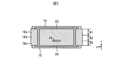
- FIG. 3 is a cross-sectional structure diagram along AA in FIG. 2.
- FIG. 3 is a cross-sectional structure diagram along BB in FIG. 2.
- FIG. 1 is an external perspective view of a high-frequency signal transmission line 10 according to an embodiment of the present invention.
- FIG. 2 is an exploded view of the dielectric body 12 of the high-frequency signal line 10 of FIG.
- FIG. 3 is a cross-sectional structural view taken along line AA in FIG.
- FIG. 4 is a cross-sectional structural view taken along line BB in FIG.
- the stacking direction of the high-frequency signal transmission line 10 is defined as the z-axis direction.
- the longitudinal direction of the high-frequency signal transmission line 10 is defined as the x-axis direction, and the direction orthogonal to the x-axis direction and the z-axis direction is defined as the y-axis direction.
- the high-frequency signal line 10 is a flexible substrate used for connecting two high-frequency circuits in an electronic device such as a mobile phone. As shown in FIGS. 1 to 3, the high-frequency signal line 10 includes a dielectric body 12, external terminals 16a and 16b, a signal line 20, a reference ground conductor 22, an auxiliary ground conductor 24, via-hole conductors b1 to b4, B1 to B6 and connectors 100a and 100b are provided.
- the dielectric body 12 is a flexible plate-like member that extends in the x-axis direction when viewed in plan from the z-axis direction, and includes a line portion 12 a, a connection portion 12 b, 12c is included.
- the dielectric body 12 is formed by laminating a protective layer 14, dielectric sheets 18a to 18c, and a protective layer 15 in this order from the positive direction side to the negative direction side in the z-axis direction. It is a laminated body.
- the main surface on the positive direction side in the z-axis direction of the dielectric element body 12 is referred to as the front surface (second main surface), and the main surface on the negative direction side in the z-axis direction of the dielectric element body 12 is the back surface ( The first main surface).
- the line portion 12a extends in the x-axis direction.
- the connecting portions 12b and 12c are respectively connected to the negative end portion in the x-axis direction and the positive end portion in the x-axis direction of the line portion 12a, and have a rectangular shape.
- the width in the y-axis direction of the connection parts 12b and 12c is larger than the width in the y-axis direction of the line part 12a.
- the dielectric sheets 18a to 18c extend in the x-axis direction when viewed in plan from the z-axis direction, and have the same shape as the dielectric body 12.
- the dielectric sheets 18a to 18c are sheets made of flexible thermoplastic resin such as polyimide or liquid crystal polymer.
- the front surface the main surface on the positive side in the z-axis direction of the dielectric sheets 18a to 18c
- the main surface on the negative direction side in the z-axis direction of the dielectric sheets 18a to 18c is referred to as the back surface.
- the total of the thickness D1 of the dielectric sheet 18a and the thickness D2 of the dielectric sheet 18b is larger than the thickness D3 of the dielectric sheet 18c, as shown in FIGS.
- the total thickness D1 and thickness D2 is, for example, 50 ⁇ m to 300 ⁇ m.
- the sum of the thickness D1 and the thickness D2 is 150 ⁇ m.
- thickness D1 is 75 micrometers.
- the thickness D2 is 75 ⁇ m.
- the thickness D3 is, for example, 10 ⁇ m to 100 ⁇ m. In the present embodiment, the thickness D3 is 50 ⁇ m.
- the dielectric sheet 18a includes a line portion 18a-a and connecting portions 18a-b and 18a-c.
- the dielectric sheet 18b includes a line portion 18b-a and connecting portions 18b-b and 18b-c.
- the dielectric sheet 18c includes a line portion 18c-a and connection portions 18c-b and 18c-c.
- the line portions 18a-a, 18b-a, and 18c-a constitute the line portion 12a.
- the connecting portions 18a-b, 18b-b, and 18c-b constitute a connecting portion 12b.
- the connecting portions 18a-c, 18b-c, and 18c-c constitute a connecting portion 12c.
- the signal line 20 is a linear conductor that transmits a high-frequency signal and is provided in the dielectric element body 12.
- the signal line 20 is a linear conductor that is formed on the back surface of the dielectric sheet 18b and extends in the x-axis direction. As a result, the signal line 20 is positioned closer to the back surface than the front surface of the dielectric element body 12 as shown in FIGS. 3 and 4.
- the end of the signal line 20 on the negative side in the x-axis direction is located at the center of the connection 18b-b as shown in FIG. As shown in FIG. 2, the end of the signal line 20 on the positive side in the x-axis direction is located at the center of the connecting portion 18b-c.
- the signal line 20 is made of a metal material having a small specific resistance mainly composed of silver or copper.
- the signal line 20 is formed on the back surface of the dielectric sheet 18b means that the signal line 20 is formed by patterning a metal foil formed by plating on the back surface of the dielectric sheet 18b, It means that the signal line 20 is formed by patterning the metal foil attached to the surface of the dielectric sheet 18b.
- the surface roughness of the surface of the signal line 20 that is in contact with the dielectric sheet 18b is the surface roughness of the surface of the signal line 20 that is not in contact with the dielectric sheet 18b. It becomes larger than the surface roughness.
- the reference ground conductor (second ground conductor) 22 is a solid conductor layer provided between the signal line 20 and the surface of the dielectric body 12, as shown in FIGS. More specifically, the reference ground conductor 22 is formed on the surface of the dielectric sheet 18a and faces the signal line 20 via the dielectric sheets 18a and 18b. The reference ground conductor 22 is not provided with an opening at a position overlapping the signal line 20.
- the reference ground conductor 22 is made of a metal material having a small specific resistance mainly composed of silver or copper.
- the reference ground conductor 22 is formed on the surface of the dielectric sheet 18a. That is, the reference ground conductor 22 is formed by patterning a metal foil formed by plating on the surface of the dielectric sheet 18a. Alternatively, the reference ground conductor 22 is formed by patterning the metal foil attached to the surface of the dielectric sheet 18a. Further, since the surface of the reference ground conductor 22 is smoothed, the surface roughness of the surface of the reference ground conductor 22 in contact with the dielectric sheet 18a is in contact with the dielectric sheet 18a in the reference ground conductor 22. It becomes larger than the surface roughness of the non-surface.
- the reference ground conductor 22 includes a main conductor 22a and terminal conductors 22b and 22c.
- the main conductor 22a is provided on the surface of the line portion 18a-a and extends along the x-axis direction.
- the terminal conductor 22b is provided on the surface of the connecting portion 18a-b and forms a rectangular ring.
- the terminal conductor 22b is connected to the end of the main conductor 22a on the negative direction side in the x-axis direction.
- the terminal conductor 22c is provided on the surface of the connecting portion 18a-c and forms a rectangular ring.
- the terminal conductor 22c is connected to the end of the main conductor 22a on the positive direction side in the x-axis direction.
- the characteristic impedance of the high-frequency signal line 10 is determined mainly based on the facing area and distance between the signal line 20 and the reference ground conductor 22 and the relative permittivity of the dielectric sheets 18a to 18c. Therefore, when setting the characteristic impedance of the high-frequency signal line 10 to 50 ⁇ , for example, the signal line 20 and the reference ground conductor 22 are designed so that the characteristic impedance of the high-frequency signal line 10a is 55 ⁇ , which is slightly higher than 50 ⁇ . .
- the shape (the size and the like of the opening 30) and the position of the auxiliary ground conductor 24 described later are adjusted so that the characteristic impedance of the high-frequency signal line 10a is 50 ⁇ by the signal line 20, the reference ground conductor 22, and the auxiliary ground conductor 24.
- the reference ground conductor 22 serves as a reference ground conductor.
- the auxiliary ground conductor (first ground conductor) 24 is a conductor layer provided between the signal line 20 and the back surface of the dielectric body 12, as shown in FIG. More specifically, the auxiliary ground conductor 24 is formed on the back surface of the dielectric sheet 18c and faces the signal line 20 via the dielectric sheet 18c.
- the auxiliary ground conductor 24 is made of a metal material having a small specific resistance mainly composed of silver or copper.
- the auxiliary ground conductor 24 is formed on the back surface of the dielectric sheet 18c means that the auxiliary ground conductor 24 is formed by patterning a metal foil formed by plating on the back surface of the dielectric sheet 18c. Alternatively, it means that the auxiliary ground conductor 24 is formed by patterning a metal foil attached to the back surface of the dielectric sheet 18c. Further, since the surface of the auxiliary ground conductor 24 is smoothed, the surface roughness of the surface of the auxiliary ground conductor 24 that is in contact with the dielectric sheet 18 c is in contact with the dielectric sheet 18 c at the auxiliary ground conductor 24. It becomes larger than the surface roughness of the non-surface.
- the auxiliary ground conductor 24 is composed of a main conductor 24a and terminal conductors 24b and 24c as shown in FIG.
- the main conductor 24a is provided on the back surface of the line portion 18c-a, and extends along the x-axis direction.
- the terminal conductor 24b is provided on the back surface of the connecting portion 18c-b and forms a rectangular ring.
- the terminal conductor 24b is connected to the end of the main conductor 24a on the negative side in the x-axis direction.
- the terminal conductor 24c is provided on the back surface of the connecting portion 18c-c and forms a rectangular ring.
- the terminal conductor 24c is connected to the end of the main conductor 24a on the positive side in the x-axis direction.
- the main conductor 24a is provided with a plurality of openings 30 arranged along the x-axis direction and having a rectangular shape.
- the main conductor 24a has a ladder shape.
- a portion of the auxiliary ground conductor 24 sandwiched between adjacent openings 30 is referred to as a bridge portion 60.
- the bridge part 60 extends in the y-axis direction.
- the plurality of openings 30 and the plurality of bridge portions 60 alternately overlap the signal line 20 when viewed in plan from the z-axis direction.
- the signal line 20 crosses the center of the opening 30 and the bridge portion 60 in the y-axis direction in the x-axis direction.
- the auxiliary ground conductor 24 is an auxiliary ground conductor that also functions as a shield. Further, as described above, the auxiliary ground conductor 24 is designed for final adjustment so that the characteristic impedance of the high-frequency signal transmission line 10 is 50 ⁇ .
- the reference ground conductor 22 is not provided with an opening, and the auxiliary ground conductor 24 is provided with an opening 30. Therefore, the area where the auxiliary ground conductor 24 and the signal line 20 are opposed is smaller than the area where the reference ground conductor 22 and the signal line 20 are opposed.
- the external terminal 16a is a rectangular conductor formed in the center on the surface of the connecting portion 18a-b. Therefore, the external terminal 16a overlaps the end of the signal line 20 on the negative direction side in the x-axis direction when viewed in plan from the z-axis direction.
- the external terminal 16b is a rectangular conductor formed at the center on the surface of the connecting portion 18a-c. Therefore, the external terminal 16b overlaps the end of the signal line 20 on the positive direction side in the x-axis direction when viewed in plan from the z-axis direction.
- the external terminals 16a and 16b are made of a metal material having a small specific resistance mainly composed of silver or copper. Further, Ni / Au plating is applied to the surfaces of the external terminals 16a and 16b.
- the external terminals 16a and 16b are formed on the surface of the dielectric sheet 18a.
- the metal foil formed by plating on the surface of the dielectric sheet 18a is patterned to form the external terminals 16a and 16b. It indicates that the external terminals 16a and 16b are formed by patterning the metal foil attached to the surface of the dielectric sheet 18a. Since the surfaces of the external terminals 16a and 16b are smoothed, the surface roughness of the surface where the external terminals 16a and 16b are in contact with the dielectric sheet 18a is the same as that of the external terminals 16a and 16b. It becomes larger than the surface roughness of the non-contact surface.
- External terminals 16a and 16b, signal line 20, reference ground conductor 22 and auxiliary ground conductor 24 have substantially the same thickness.
- the thicknesses of the external terminals 16a and 16b, the signal line 20, the reference ground conductor 22, and the auxiliary ground conductor 24 are, for example, 10 ⁇ m to 20 ⁇ m.
- the signal line 20 is sandwiched between the reference ground conductor 22 and the auxiliary ground conductor 24 from both sides in the z-axis direction. That is, the signal line 20, the reference ground conductor 22, and the auxiliary ground conductor 24 have a triplate type stripline structure.
- the distance between the signal line 20 and the reference ground conductor 22 is the sum of the thickness D1 of the dielectric sheet 18a and the thickness D2 of the dielectric sheet 18b as shown in FIGS. For example, 50 ⁇ m to 300 ⁇ m. In the present embodiment, the distance between the signal line 20 and the reference ground conductor 22 is 150 ⁇ m.
- the distance (distance in the z-axis direction) between the signal line 20 and the auxiliary ground conductor 24 is substantially equal to the thickness D3 of the dielectric sheet 18c as shown in FIGS. 3 and 4, for example, 10 ⁇ m to 100 ⁇ m. .
- the distance between the signal line 20 and the auxiliary ground conductor 24 is 50 ⁇ m. Therefore, the distance in the z-axis direction between the signal line 20 and the auxiliary ground conductor 24 is smaller than the distance in the z-axis direction between the signal line 20 and the reference ground conductor 22.
- the plurality of via-hole conductors B1 pass through the dielectric sheet 18a in the z-axis direction on the positive side in the y-axis direction from the signal line 20, and are evenly spaced in a line in the x-axis direction.
- the plurality of via-hole conductors B2 pass through the dielectric sheet 18b in the z-axis direction on the positive side in the y-axis direction from the signal line 20, and are evenly spaced in a line in the x-axis direction.
- the plurality of via-hole conductors B3 pass through the dielectric sheet 18c in the z-axis direction on the positive side in the y-axis direction from the signal line 20, and are evenly spaced in a line in the x-axis direction. Are lined up.
- the via hole conductors B1 to B3 are connected to each other to form one via hole conductor.
- the end of the via-hole conductor B1 on the positive side in the z-axis direction is connected to the reference ground conductor 22.
- the end of the via-hole conductor B3 on the negative side in the z-axis direction is connected to the auxiliary ground conductor 24.
- the via-hole conductor B3 is connected to the auxiliary ground conductor 24 on the positive side in the y-axis direction from the bridge portion 60.
- the via-hole conductors B1 to B3 are formed by filling the via holes formed in the dielectric sheets 18a to 18c with a conductive paste containing silver, tin, copper, or the like as a main component and solidifying.
- the plurality of via-hole conductors B4 pass through the dielectric sheet 18a in the z-axis direction on the negative side in the y-axis direction from the signal line 20, and are equally spaced in a line in the x-axis direction.
- the plurality of via-hole conductors B5 pass through the dielectric sheet 18b in the z-axis direction on the negative side in the y-axis direction from the signal line 20, and are equally spaced in a line in the x-axis direction.
- the plurality of via-hole conductors B6 pass through the dielectric sheet 18c in the z-axis direction on the negative side in the y-axis direction from the signal line 20, and are evenly spaced in a line in the x-axis direction. Are lined up. Via-hole conductors B4 to B6 are connected to each other to form one via-hole conductor. The end of the via-hole conductor B4 on the positive side in the z-axis direction is connected to the reference ground conductor 22. The end of the via-hole conductor B6 on the negative side in the z-axis direction is connected to the auxiliary ground conductor 24.
- the via-hole conductor B6 is connected to the auxiliary ground conductor 24 on the negative direction side in the y-axis direction from the bridge portion 60.
- the via-hole conductors B4 to B6 are formed by filling the via holes formed in the dielectric sheets 18a to 18c with a conductive paste mainly composed of silver, tin, copper, or the like and solidifying the via holes.
- the via-hole conductor b1 passes through the connecting portions 18a-b of the dielectric sheet 18a in the z-axis direction.
- the via-hole conductor b3 penetrates the connecting portion 18b-b of the dielectric sheet 18b in the z-axis direction.
- Via-hole conductors b1 and b3 are connected to each other to form one via-hole conductor.
- the end of the via-hole conductor b1 on the positive side in the z-axis direction is connected to the external terminal 16a.
- the end of the via-hole conductor b3 on the negative direction side in the z-axis direction is connected to the end of the signal line 20 on the negative direction side in the x-axis direction.
- the via-hole conductor b2 passes through the connecting portions 18a-c of the dielectric sheet 18a in the z-axis direction.
- the via-hole conductor b4 passes through the connecting portion 18b-c of the dielectric sheet 18b in the z-axis direction.
- the via-hole conductors b2 and b4 are connected to each other to constitute one via-hole conductor.
- the end of the via-hole conductor b2 on the positive side in the z-axis direction is connected to the external terminal 16b.
- the end portion on the negative direction side in the z-axis direction of the via-hole conductor b4 is connected to the end portion on the positive direction side in the x-axis direction of the signal line 20.
- the via-hole conductors b1 to b4 are formed by filling the via holes formed in the dielectric sheets 18a and 18b with a conductive paste mainly composed of silver, tin, copper, or the like and solidifying them.
- the protective layer 14 is an insulating film provided on the surface of the dielectric sheet 18a and covers substantially the entire surface of the dielectric sheet 18a. Thereby, the protective layer 14 covers the reference ground conductor 22.
- the protective layer 14 is made of a flexible resin such as a resist material, for example.
- the protective layer 14 includes a line portion 14a and connecting portions 14b and 14c.
- the line portion 14a covers the main conductor 22a by covering the entire surface of the line portion 18a-a.
- the connecting portion 14b is connected to the end portion on the negative side in the x-axis direction of the line portion 14a and covers the surface of the connecting portion 18a-b.
- openings Ha to Hd are provided in the connection portion 14b.
- the opening Ha is a rectangular opening provided in the center of the connection portion 14b.
- the external terminal 16a is exposed to the outside through the opening Ha.
- the opening Hb is a rectangular opening provided on the positive side in the y-axis direction with respect to the opening Ha.
- the opening Hc is a rectangular opening provided on the negative direction side in the x-axis direction from the opening Ha.
- the opening Hd is a rectangular opening provided on the negative side in the y-axis direction with respect to the opening Ha.
- the terminal conductor 22b functions as an external terminal by being exposed to the outside through the openings Hb to Hd.
- the connecting portion 14c is connected to the end portion on the positive side in the x-axis direction of the line portion 14a and covers the surface of the connecting portion 18a-c.
- openings He to Hh are provided in the connection portion 14c.
- the opening He is a rectangular opening provided in the center of the connection portion 14c.
- the external terminal 16b is exposed to the outside through the opening He.
- the opening Hf is a rectangular opening provided on the positive direction side in the y-axis direction with respect to the opening He.
- the opening Hg is a rectangular opening provided closer to the positive direction side in the x-axis direction than the opening He.
- the opening Hh is a rectangular opening provided on the negative side in the y-axis direction with respect to the opening He.
- the terminal conductor 22c functions as an external terminal by being exposed to the outside through the openings Hf to Hh.
- the protective layer 15 is an insulating film provided on the back surface of the dielectric sheet 18c, and covers substantially the entire back surface of the dielectric sheet 18c. Thereby, the protective layer 15 covers the auxiliary ground conductor 24.
- the protective layer 15 is made of a flexible resin such as a resist material, for example.
- the characteristic impedance of the signal line 20 periodically varies between the impedance Z1 and the impedance Z2. More specifically, a relatively small capacitance is formed between the signal line 20 and the auxiliary ground conductor 24 in the section A ⁇ b> 1 overlapping the opening 30 in the signal line 20. Therefore, the characteristic impedance of the signal line 20 in the section A1 is a relatively high impedance Z1.
- the characteristic impedance of the signal line 20 in the section A2 is a relatively low impedance Z2.
- the section A1 and the section A2 are alternately arranged in the x-axis direction. Therefore, the characteristic impedance of the signal line 20 periodically varies between the impedance Z1 and the impedance Z2.
- the impedance Z1 is, for example, 55 ⁇
- the impedance Z2 is, for example, 45 ⁇ .
- the average characteristic impedance of the entire signal line 20 is, for example, 50 ⁇ .
- FIG. 5 is an external perspective view of the connector 100 b of the high-frequency signal transmission line 10.
- FIG. 6 is a cross-sectional structure diagram of the connector 100 b of the high-frequency signal transmission line 10.
- the connector 100b includes a connector main body 102, external terminals 104 and 106, a central conductor 108, and an external conductor 110, as shown in FIGS.
- the connector main body 102 has a shape in which a cylindrical member is connected to a rectangular plate member, and is made of an insulating material such as a resin.
- the external terminal 104 is provided at a position facing the external terminal 16b on the negative side surface in the z-axis direction of the plate member of the connector main body 102.
- the external terminal 106 is provided at a position facing the terminal conductor 22c exposed through the openings Hf to Hh on the negative side surface in the z-axis direction of the plate member of the connector main body 102.
- the center conductor 108 is provided at the center of the cylindrical member of the connector main body 102 and is connected to the external terminal 104.
- the center conductor 108 is a signal terminal for inputting or outputting a high frequency signal.
- the external conductor 110 is provided on the inner peripheral surface of the cylindrical member of the connector main body 102 and is connected to the external terminal 106.
- the outer conductor 110 is a ground terminal that is maintained at a ground potential.
- the connector 100 b configured as described above has the connection portion 12 c such that the external terminal 104 is connected to the external terminal 16 b and the external terminal 106 is connected to the terminal conductor 22 c. Mounted on the surface. Thereby, the signal line 20 is electrically connected to the central conductor 108. Further, the reference ground conductor 22 and the auxiliary ground conductor 24 are electrically connected to the external conductor 110.
- FIG. 7 is a plan view of the electronic device 200 using the high-frequency signal transmission line 10 from the y-axis direction.
- FIG. 8 is a plan view of the electronic device 200 using the high-frequency signal transmission line 10 from the z-axis direction.
- FIG. 9 is an enlarged view of FIG. 7C.
- the electronic device 200 includes the high-frequency signal line 10, circuit boards 202 a and 202 b, receptacles 204 a and 204 b, a battery pack (metal body) 206, and a housing 210.
- the housing 210 houses the high-frequency signal line 10, circuit boards 202 a and 202 b, receptacles 204 a and 204 b, and a battery pack 206.
- the circuit board 202a is provided with, for example, a transmission circuit or a reception circuit including an antenna.
- a power supply circuit is provided on the circuit board 202b.
- the battery pack 206 is a lithium ion secondary battery, for example, and has a structure in which the surface is covered with a metal cover.
- the circuit board 202a, the battery pack 206, and the circuit board 202b are arranged in this order from the negative direction side to the positive direction side in the x-axis direction.
- the receptacles 204a and 204b are provided on the main surfaces of the circuit boards 202a and 202b on the negative side in the z-axis direction, respectively.
- Connectors 100a and 100b are connected to receptacles 204a and 204b, respectively. At this time, the line portion 12a is bent as described below.
- the positive direction side of the line portion 12 a from the center in the x-axis direction is mountain-folded with respect to the back surface of the dielectric element body 12 at a mountain fold line that intersects the signal line 20. Accordingly, the dielectric body 12 is along the surface of the battery pack 206 on the negative direction side in the z-axis direction and the side surface of the battery pack 206 on the positive direction side in the x-axis direction.
- a section where the dielectric body 12 is folded is referred to as a section A ⁇ b> 11.
- the portion on the positive side in the x-axis direction from the section A11 is a valley with respect to the back surface of the dielectric element body 12 in the valley fold line intersecting the signal line 20, as shown in FIG. It is folded.
- the dielectric body 12 is drawn out from the side surface on the positive direction side in the x-axis direction of the battery pack 206 onto the main surface on the negative direction side in the z-axis direction of the circuit board 202b.
- a section where the dielectric body 12 is valley-folded is referred to as a section A12.
- the average of the radius of curvature R1 of the section A11 in the dielectric body 12 is larger than the average of the radius of curvature R2 of the section A12 in the dielectric body 12.
- the radius of curvature means the radius of curvature of the imaginary line L that passes through the center of the dielectric element body 12 in the z-axis direction. Since the high-frequency signal line 10 has such a structure, occurrence of disconnection in the signal line 20 is suppressed as will be described later.
- the negative side with respect to the center in the x-axis direction of the line portion 12a is also mountain-folded and valley-shaped with respect to the back surface of the dielectric element body 12, similarly to the positive direction side with respect to the center in the x-axis direction of the line portion 12a. It is folded.
- the method of folding the line portion 12a near the end on the negative side in the x-axis direction is the same as the method of folding the line portion 12a near the end on the positive direction side in the x-axis direction, and thus the description thereof is omitted. To do.
- the center conductor 108 of the connectors 100a and 100b has a frequency of, for example, 2 GHz transmitted between the circuit boards 202a and 202b.
- a high frequency signal is applied through the receptacles 204a, 204b.
- the external conductor 110 of the connectors 100a and 100b is kept at the ground potential via the circuit boards 202a and 202b and the receptacles 204a and 204b. Thereby, the high-frequency signal transmission line 10 connects between the circuit boards 202a and 202b.
- the surface of the dielectric body 12 (more precisely, the protective layer 14) is in contact with the battery pack 206.
- the dielectric body 12 and the battery pack 206 are fixed with an adhesive or the like.
- a solid reference ground conductor 22 having no opening exists between the signal line 20 and the battery pack 206.
- FIG. 10 is a process diagram when the high-frequency signal transmission line 10 is bent.
- a case where one high-frequency signal line 10 is manufactured will be described as an example, but actually, a plurality of high-frequency signal lines 10 are simultaneously manufactured by laminating and cutting large-sized dielectric sheets. .
- dielectric sheets 18a to 18c made of a thermoplastic resin in which a copper foil (metal film) is formed on the entire surface of one main surface are prepared. Specifically, a copper foil is attached to one main surface of the dielectric sheets 18a to 18c. Further, the surface of the copper foil of the dielectric sheets 18a to 18c is smoothed by, for example, applying a zinc plating for rust prevention.
- the dielectric sheets 18a to 18c are liquid crystal polymers.
- the thickness of the copper foil is 10 ⁇ m to 20 ⁇ m.
- the external terminals 16a and 16b and the reference ground conductor 22 are formed on the surface of the dielectric sheet 18a as shown in FIG. .
- a resist having the same shape as the external terminals 16a and 16b and the reference ground conductor 22 shown in FIG. 2 is printed on the copper foil on the surface of the dielectric sheet 18a.
- the copper foil of the part which is not covered with the resist is removed by performing an etching process with respect to copper foil. Thereafter, the resist is removed by spraying a cleaning liquid (resist removing liquid).
- a cleaning liquid resist removing liquid
- the signal line 20 is formed on the back surface of the dielectric sheet 18b. Further, as shown in FIG. 2, the auxiliary ground conductor 24 is formed on the back surface of the dielectric sheet 18c.
- the formation process of the signal line 20 and the auxiliary ground conductor 24 is the same as the formation process of the external terminals 16a and 16b, the signal line 20, and the reference ground conductor 22, the description is omitted.
- through holes are formed by irradiating laser beams to positions where the via-hole conductors b1 to b4 and B1 to B6 of the dielectric sheets 18a to 18c are formed. Then, the through hole is filled with a conductive paste to form via-hole conductors b1 to b4 and B1 to B6.
- the dielectric sheets 18a to 18c are stacked in this order from the positive direction side to the negative direction side in the z-axis direction, and subjected to a crimping process and a heating process.
- the dielectric sheets 18a to 18c are softened and the conductive paste in the through holes is solidified.
- the dielectric sheets 18a to 18c are joined, and the via-hole conductors b1 to b4 and B1 to B6 are formed.
- a protective layer 14 covering the reference ground conductor 22 is formed on the surface of the dielectric sheet 18a by applying a resin (resist) paste by screen printing.
- a protective layer 15 covering the auxiliary ground conductor 24 is formed on the back surface of the dielectric sheet 18c by applying a resin (resist) paste by screen printing.
- the connectors 100a and 100b are mounted on the external terminals 16a and 16b and the terminal conductors 22b and 22c on the connecting portions 12b and 12c by using solder.
- both ends in the x-axis direction of the line portion 12a are mountain-folded and valley-folded by sandwiching the line portion 12a from both sides in the z-axis direction with the crimping tools T1 and T2.
- the crimping tool T1 is a tool that comes into contact with the back surface of the line portion 12a, and has steps for performing mountain folds and valley folds on the line portion 12a.
- the corner on the valley side of the crimping tool T1 is referred to as a corner C1
- the corner on the mountain side of the crimping tool T1 is referred to as a corner C2.
- the corners C1 and C2 are chamfered.
- the curvature radius of the corner C1 is the curvature radius r1.
- the radius of curvature of the corner C2 is a radius of curvature r2.
- the crimping tool T2 is a tool that comes into contact with the surface of the line portion 12a, and has a step for making a mountain fold and a valley fold with respect to the line portion 12a.
- the crest side corner of the crimping tool T2 is referred to as a corner C3
- the trough side corner of the crimping tool T2 is referred to as a corner C4.
- the corners C3 and C4 are chamfered.
- the curvature radius of the corner C3 is the curvature radius r3.
- the average of the curvature radius r3 is larger than the average of the curvature radius r2.
- the curvature radius of the corner C4 is the curvature radius r4.
- the average of the curvature radius r1 is larger than the average of the curvature radius r4.
- the crimping tools T1 and T2 configured as described above are arranged so that the corner C1 and the corner C3 substantially coincide with each other and the corner C2 and the corner C4 substantially coincide with each other in the z-axis direction. Then, the line portion 12a is sandwiched from both sides in the z-axis direction by the crimping tools T1 and T2.
- the crimping tools T1 and T2 have built-in heaters, and it is preferable to heat the line portion 12a with the crimping tools T1 and T2. Thereby, a mountain fold and a valley fold are given to the track part 12a.
- the curvature radius R1 of the section A11 where the dielectric element body 12 is folded in a mountain is larger than the curvature radius R2 of the section A12 where the dielectric element body 12 is folded.
- the high-frequency signal transmission line 10 subjected to the mountain fold and the valley fold as described above is connected to the receptacles 204a and 204b.
- the signal line is disposed closer to the other main surface than one main surface of the dielectric body. For this reason, when the high-frequency signal line is folded up with respect to the other main surface, the signal line (signal line) is pulled. On the other hand, when the high-frequency signal line is valley-folded with respect to the other main surface, the signal line is compressed. Here, when the signal line is pulled, the signal line is more likely to be disconnected than when the signal line is compressed.
- the curvature radius R1 of the section A11 where the dielectric element body 12 is folded in a mountain is the curvature radius of the section A12 where the dielectric element body 12 is valley-folded. It is larger than R2.
- the high-frequency signal transmission line 10 it is possible to reduce the thickness. More specifically, in the high-frequency signal transmission line 10, in the section A1, the signal transmission line 20 does not overlap with the auxiliary ground conductor 24 when viewed in plan from the z-axis direction. Therefore, it is difficult to form a capacitance between the signal line 20 and the auxiliary ground conductor 24. Therefore, even if the distance between the signal line 20 and the auxiliary ground conductor 24 in the z-axis direction is reduced, the capacitance formed between the signal line 20 and the auxiliary ground conductor 24 does not become too large. Therefore, the characteristic impedance of the signal line 20 is unlikely to deviate from a predetermined characteristic impedance (for example, 50 ⁇ ). As a result, according to the high frequency signal line 10, it is possible to reduce the thickness while maintaining the characteristic impedance of the signal line 20 at a predetermined characteristic impedance.
- a predetermined characteristic impedance for example, 50 ⁇
- the high-frequency signal line 10 when the high-frequency signal line 10 is attached to a metal body such as the battery pack 206, the characteristic impedance of the signal line 20 is suppressed from fluctuating. More specifically, the high-frequency signal line 10 is attached to the battery pack 206 so that the solid reference ground conductor 22 is positioned between the signal line 20 and the battery pack 206. As a result, the signal line 20 and the battery pack 206 do not face each other through the opening, and the formation of a capacitance between the signal line 20 and the battery pack 206 is suppressed. As a result, the high frequency signal line 10 is affixed to the battery pack 206, thereby suppressing the characteristic impedance of the signal line 20 from being lowered.
- the flexible substrate and the electronic device according to the present invention are not limited to the high-frequency signal line 10 and the electronic device 200 but can be changed within the scope of the gist thereof.
- the protective layers 14 and 15 are formed by screen printing, but may be formed by a photolithography process.
- the connectors 100a and 100b do not have to be mounted. In this case, the end of the high-frequency signal line 10 and the circuit board are connected by solder or the like.
- the connector 100a or the connector 100b may be mounted only on one end of the high-frequency signal line 10.
- the connectors 100a and 100b are mounted on the surface of the high-frequency signal line 10, but may be mounted on the back surface of the high-frequency signal line 10. Further, the connector 100 a may be mounted on the front surface of the high frequency signal line 10 and the connector 100 b may be mounted on the back surface of the high frequency signal line 10.
- one or both of the reference ground conductor 22 and the auxiliary ground conductor 24 may not be provided.
- the auxiliary ground conductor 24 may be provided on the surface of the dielectric sheet 18b.
- the high-frequency signal line 10 may be used as a high-frequency signal line in an RF circuit board such as an antenna front end module.
- the signal line 20 is not a signal line through which a high-frequency signal is transmitted, but may be, for example, a power supply line used for supplying power, a ground line maintained at a ground potential, or the like.
- the present invention is useful for flexible substrates and electronic devices, and is excellent in that the occurrence of disconnection in a signal line can be suppressed.
Abstract
Description
以下に、本発明の一実施形態に係る高周波信号線路の構成について図面を参照しながら説明する。図1は、本発明の一実施形態に係る高周波信号線路10の外観斜視図である。図2は、図1の高周波信号線路10の誘電体素体12の分解図である。図3は、図2のA-Aにおける断面構造図である。図4は、図2のB-Bにおける断面構造図である。以下では、高周波信号線路10の積層方向をz軸方向と定義する。また、高周波信号線路10の長手方向をx軸方向と定義し、x軸方向及びz軸方向に直交する方向をy軸方向と定義する。 (Configuration of high-frequency signal line)
The configuration of the high-frequency signal line according to one embodiment of the present invention will be described below with reference to the drawings. FIG. 1 is an external perspective view of a high-frequency
以下に、高周波信号線路10の製造方法について図面を参照しながら説明する。図10は、高周波信号線路10が折り曲げられる際の工程図である。以下では、一つの高周波信号線路10が作製される場合を例にとって説明するが、実際には、大判の誘電体シートが積層及びカットされることにより、同時に複数の高周波信号線路10が作製される。 (Manufacturing method of high frequency signal line)
Below, the manufacturing method of the high frequency signal track |
以上のように構成された高周波信号線路10によれば、信号線路20に断線が発生することを抑制できる。より詳細には、特許文献1に記載の高周波信号線路では、信号線は、誘電体素体の一方の主面よりも他方の主面の近くに配置されている。そのため、高周波信号線路が他方の主面に対して山折りされると、信号線(信号線路)が引っ張られる。一方、高周波信号線路が他方の主面に対して谷折りされると、信号線が圧縮される。ここで、信号線が引っ張られた場合の方が、信号線が圧縮された場合よりも、信号線に断線が発生しやすい。 (effect)
According to the high-frequency
本発明に係るフレキシブル基板及び電子機器は、高周波信号線路10及び電子機器200に限らず、その要旨の範囲内において変更可能である。 (Other embodiments)
The flexible substrate and the electronic device according to the present invention are not limited to the high-
10 高周波信号線路
12 誘電体素体
20 信号線路
22 基準グランド導体
24 補助グランド導体
30 開口
60 ブリッジ部
200 電子機器
210 筐体 A1, A2, A11, A12
Claims (5)
- 第1の主面及び第2の主面を有し、かつ、可撓性を有する本体と、
前記第2の主面よりも前記第1の主面の近くに位置するように前記本体に設けられている線状導体と、
を備えており、
前記本体は、前記線状導体に交差する谷折り線において、前記第1の主面に対して谷折りされていると共に、該線状導体に交差する山折り線において、該第1の主面に対して山折りされており、
前記本体において山折りされている区間の曲率半径の平均は、該本体において谷折りされている区間の曲率半径の平均よりも大きいこと、
を特徴とするフレキシブル基板。 A main body having a first main surface and a second main surface and having flexibility;
A linear conductor provided in the main body so as to be positioned closer to the first main surface than the second main surface;
With
The main body is valley-folded with respect to the first main surface at a valley fold line that intersects the linear conductor, and the first main surface at a mountain fold line that intersects the linear conductor. Against the mountain,
The average radius of curvature of the section folded in the main body is larger than the average radius of curvature of the section folded in the main body;
A flexible substrate characterized by - 前記線状導体と前記第1の主面との間に設けられている第1のグランド導体と、
前記線状導体と前記第2の主面との間に設けられている第2のグランド導体と、
を更に備えており、
前記第1のグランド導体と前記線状導体との距離は、前記第2のグランド導体と前記線状導体との距離よりも小さいこと、
を特徴とする請求項1に記載のフレキシブル基板。 A first ground conductor provided between the linear conductor and the first main surface;
A second ground conductor provided between the linear conductor and the second main surface;
Is further provided,
A distance between the first ground conductor and the linear conductor is smaller than a distance between the second ground conductor and the linear conductor;
The flexible substrate according to claim 1. - 前記第1のグランド導体と前記線状導体とが対向している面積は、前記第2のグランド導体と該線状導体とが対向している面積よりも小さいこと、
を特徴とする請求項2に記載のフレキシブル基板。 The area where the first ground conductor and the linear conductor face each other is smaller than the area where the second ground conductor and the linear conductor face each other;
The flexible substrate according to claim 2. - 前記本体は、熱可塑性樹脂により作製されていること、
を特徴とする請求項1ないし請求項3のいずれかに記載のフレキシブル基板。 The body is made of a thermoplastic resin;
The flexible substrate according to any one of claims 1 to 3, wherein: - 筐体と、
前記筐体に収容されているフレキシブル基板と、
を備えており、
前記フレキシブル基板は、
第1の主面及び第2の主面を有し、かつ、可撓性を有する本体と、
前記第2の主面よりも前記第1の主面の近くに位置するように前記本体に設けられている線状導体と、
を備えており、
前記本体は、前記線状導体に交差する谷折り線において、前記第1の主面に対して谷折りされていると共に、該線状導体に交差する山折り線において、該第1の主面に対して山折りされており、
前記本体において山折りされている区間の曲率半径の平均は、該本体において谷折りされている区間の曲率半径の平均よりも大きいこと、
を特徴とする電子機器。 A housing,
A flexible substrate housed in the housing;
With
The flexible substrate is
A main body having a first main surface and a second main surface and having flexibility;
A linear conductor provided in the main body so as to be positioned closer to the first main surface than the second main surface;
With
The main body is valley-folded with respect to the first main surface at a valley fold line that intersects the linear conductor, and the first main surface at a mountain fold line that intersects the linear conductor. Against the mountain,
The average radius of curvature of the section folded in the main body is larger than the average radius of curvature of the section folded in the main body;
Electronic equipment characterized by
Priority Applications (3)
| Application Number | Priority Date | Filing Date | Title |
|---|---|---|---|
| CN201390000424.7U CN204559998U (en) | 2012-12-12 | 2013-12-12 | Flexible base, board and electronic equipment |
| JP2014528350A JP5610110B1 (en) | 2012-12-12 | 2013-12-12 | Flexible substrate and electronic device |
| US14/499,501 US9113556B2 (en) | 2012-12-12 | 2014-09-29 | Flexible board and electronic device |
Applications Claiming Priority (2)
| Application Number | Priority Date | Filing Date | Title |
|---|---|---|---|
| JP2012-270938 | 2012-12-12 | ||
| JP2012270938 | 2012-12-12 |
Related Child Applications (1)
| Application Number | Title | Priority Date | Filing Date |
|---|---|---|---|
| US14/499,501 Continuation US9113556B2 (en) | 2012-12-12 | 2014-09-29 | Flexible board and electronic device |
Publications (1)
| Publication Number | Publication Date |
|---|---|
| WO2014092153A1 true WO2014092153A1 (en) | 2014-06-19 |
Family
ID=50934436
Family Applications (1)
| Application Number | Title | Priority Date | Filing Date |
|---|---|---|---|
| PCT/JP2013/083329 WO2014092153A1 (en) | 2012-12-12 | 2013-12-12 | Flexible substrate and electronic device |
Country Status (4)
| Country | Link |
|---|---|
| US (1) | US9113556B2 (en) |
| JP (1) | JP5610110B1 (en) |
| CN (1) | CN204559998U (en) |
| WO (1) | WO2014092153A1 (en) |
Cited By (4)
| Publication number | Priority date | Publication date | Assignee | Title |
|---|---|---|---|---|
| JP6070909B2 (en) * | 2014-12-01 | 2017-02-01 | 株式会社村田製作所 | Electronic device, electrical element and tray for electrical element |
| JPWO2016052125A1 (en) * | 2014-09-30 | 2017-04-27 | 株式会社村田製作所 | Electronics |
| JP2019009287A (en) * | 2017-06-26 | 2019-01-17 | パナソニックIpマネジメント株式会社 | Mounting base, component mounting module and moving body |
| JP7456504B2 (en) | 2020-07-21 | 2024-03-27 | 株式会社村田製作所 | Resin multilayer board and method for manufacturing resin multilayer board |
Families Citing this family (6)
| Publication number | Priority date | Publication date | Assignee | Title |
|---|---|---|---|---|
| WO2016056496A1 (en) * | 2014-10-10 | 2016-04-14 | 株式会社村田製作所 | Transmission line, and flat cable |
| JP6504828B2 (en) * | 2015-01-16 | 2019-04-24 | 日本メクトロン株式会社 | Flexible printed circuit board and method of manufacturing flexible printed circuit board |
| CN106862350A (en) * | 2017-03-14 | 2017-06-20 | 昂纳信息技术(深圳)有限公司 | A kind of flexible board bending device and its bending technique |
| WO2018213494A1 (en) * | 2017-05-16 | 2018-11-22 | Rigetti & Co, Inc. | Connecting electrical circuitry in a quantum computing system |
| JP6732723B2 (en) * | 2017-12-14 | 2020-07-29 | 日本メクトロン株式会社 | Printed wiring board for high frequency transmission |
| USD886073S1 (en) * | 2018-01-29 | 2020-06-02 | Gigalane Co., Ltd. | Flexible printed circuit board |
Citations (2)
| Publication number | Priority date | Publication date | Assignee | Title |
|---|---|---|---|---|
| JP2008235593A (en) * | 2007-03-20 | 2008-10-02 | Sumitomo Electric Printed Circuit Inc | Flexible printed wiring board |
| JP2009176901A (en) * | 2008-01-23 | 2009-08-06 | Casio Hitachi Mobile Communications Co Ltd | Flexible circuit board and electronic equipment |
Family Cites Families (4)
| Publication number | Priority date | Publication date | Assignee | Title |
|---|---|---|---|---|
| JP2006294350A (en) * | 2005-04-07 | 2006-10-26 | Three M Innovative Properties Co | Cable harness body |
| JP2007123428A (en) * | 2005-10-26 | 2007-05-17 | Nec Electronics Corp | Flexible circuit board |
| JP2009008758A (en) * | 2007-06-26 | 2009-01-15 | Fujinon Corp | Imaging device, camera module and portable terminal equipment |
| CN102687600B (en) | 2010-12-03 | 2014-04-02 | 株式会社村田制作所 | High-frequency signal line |
-
2013
- 2013-12-12 WO PCT/JP2013/083329 patent/WO2014092153A1/en active Application Filing
- 2013-12-12 JP JP2014528350A patent/JP5610110B1/en active Active
- 2013-12-12 CN CN201390000424.7U patent/CN204559998U/en not_active Expired - Lifetime
-
2014
- 2014-09-29 US US14/499,501 patent/US9113556B2/en active Active
Patent Citations (2)
| Publication number | Priority date | Publication date | Assignee | Title |
|---|---|---|---|---|
| JP2008235593A (en) * | 2007-03-20 | 2008-10-02 | Sumitomo Electric Printed Circuit Inc | Flexible printed wiring board |
| JP2009176901A (en) * | 2008-01-23 | 2009-08-06 | Casio Hitachi Mobile Communications Co Ltd | Flexible circuit board and electronic equipment |
Cited By (7)
| Publication number | Priority date | Publication date | Assignee | Title |
|---|---|---|---|---|
| JPWO2016052125A1 (en) * | 2014-09-30 | 2017-04-27 | 株式会社村田製作所 | Electronics |
| JP6070909B2 (en) * | 2014-12-01 | 2017-02-01 | 株式会社村田製作所 | Electronic device, electrical element and tray for electrical element |
| JP6070908B2 (en) * | 2014-12-01 | 2017-02-01 | 株式会社村田製作所 | Electronics |
| JPWO2016088693A1 (en) * | 2014-12-01 | 2017-04-27 | 株式会社村田製作所 | Electronics |
| JPWO2016088592A1 (en) * | 2014-12-01 | 2017-04-27 | 株式会社村田製作所 | Electronic device, electrical element and tray for electrical element |
| JP2019009287A (en) * | 2017-06-26 | 2019-01-17 | パナソニックIpマネジメント株式会社 | Mounting base, component mounting module and moving body |
| JP7456504B2 (en) | 2020-07-21 | 2024-03-27 | 株式会社村田製作所 | Resin multilayer board and method for manufacturing resin multilayer board |
Also Published As
| Publication number | Publication date |
|---|---|
| US20150018055A1 (en) | 2015-01-15 |
| JPWO2014092153A1 (en) | 2017-01-12 |
| CN204559998U (en) | 2015-08-12 |
| JP5610110B1 (en) | 2014-10-22 |
| US9113556B2 (en) | 2015-08-18 |
Similar Documents
| Publication | Publication Date | Title |
|---|---|---|
| JP5610110B1 (en) | Flexible substrate and electronic device | |
| JP5943168B2 (en) | Flexible substrate and electronic device | |
| JP2014086655A (en) | Flexible substrate | |
| JP5472556B2 (en) | High frequency signal lines and electronic equipment | |
| JPWO2013080887A1 (en) | High frequency signal line, method for manufacturing the same, and electronic device | |
| JP5867621B2 (en) | High frequency signal line and manufacturing method thereof | |
| JP6044650B2 (en) | High frequency signal transmission line and electronic equipment | |
| WO2014002764A1 (en) | Laminated flat cable and manufacturing method therefor | |
| JP5637340B2 (en) | Flat cable | |
| WO2014084011A1 (en) | High-frequency signal line and electronic device equipped with same | |
| JP5765468B2 (en) | High frequency signal line | |
| JP5704286B2 (en) | High frequency signal line | |
| JP5605528B2 (en) | High frequency signal transmission line and electronic equipment | |
| JP5655998B1 (en) | High frequency signal transmission line and electronic equipment | |
| WO2014065172A1 (en) | Flexible substrate | |
| JP5935620B2 (en) | Flat cable | |
| JP5862790B2 (en) | High frequency signal line | |
| JP5958122B2 (en) | High frequency signal line and method for manufacturing substrate layer with signal line | |
| JP2014078836A (en) | High-frequency signal line and method of manufacturing the same |
Legal Events
| Date | Code | Title | Description |
|---|---|---|---|
| WWE | Wipo information: entry into national phase |
Ref document number: 201390000424.7 Country of ref document: CN |
|
| ENP | Entry into the national phase |
Ref document number: 2014528350 Country of ref document: JP Kind code of ref document: A |
|
| 121 | Ep: the epo has been informed by wipo that ep was designated in this application |
Ref document number: 13862915 Country of ref document: EP Kind code of ref document: A1 |
|
| NENP | Non-entry into the national phase |
Ref country code: DE |
|
| 122 | Ep: pct application non-entry in european phase |
Ref document number: 13862915 Country of ref document: EP Kind code of ref document: A1 |