WO2014073572A1 - ネマチック液晶組成物及びこれを用いた液晶表示素子 - Google Patents
ネマチック液晶組成物及びこれを用いた液晶表示素子 Download PDFInfo
- Publication number
- WO2014073572A1 WO2014073572A1 PCT/JP2013/080023 JP2013080023W WO2014073572A1 WO 2014073572 A1 WO2014073572 A1 WO 2014073572A1 JP 2013080023 W JP2013080023 W JP 2013080023W WO 2014073572 A1 WO2014073572 A1 WO 2014073572A1
- Authority
- WO
- WIPO (PCT)
- Prior art keywords
- liquid crystal
- crystal composition
- group
- general formula
- crystal display
- Prior art date
- Legal status (The legal status is an assumption and is not a legal conclusion. Google has not performed a legal analysis and makes no representation as to the accuracy of the status listed.)
- Ceased
Links
- HGCIXCUEYOPUTN-UHFFFAOYSA-N C1CC=CCC1 Chemical compound C1CC=CCC1 HGCIXCUEYOPUTN-UHFFFAOYSA-N 0.000 description 1
Classifications
-
- G—PHYSICS
- G02—OPTICS
- G02F—OPTICAL DEVICES OR ARRANGEMENTS FOR THE CONTROL OF LIGHT BY MODIFICATION OF THE OPTICAL PROPERTIES OF THE MEDIA OF THE ELEMENTS INVOLVED THEREIN; NON-LINEAR OPTICS; FREQUENCY-CHANGING OF LIGHT; OPTICAL LOGIC ELEMENTS; OPTICAL ANALOGUE/DIGITAL CONVERTERS
- G02F1/00—Devices or arrangements for the control of the intensity, colour, phase, polarisation or direction of light arriving from an independent light source, e.g. switching, gating or modulating; Non-linear optics
- G02F1/01—Devices or arrangements for the control of the intensity, colour, phase, polarisation or direction of light arriving from an independent light source, e.g. switching, gating or modulating; Non-linear optics for the control of the intensity, phase, polarisation or colour
- G02F1/13—Devices or arrangements for the control of the intensity, colour, phase, polarisation or direction of light arriving from an independent light source, e.g. switching, gating or modulating; Non-linear optics for the control of the intensity, phase, polarisation or colour based on liquid crystals, e.g. single liquid crystal display cells
- G02F1/133—Constructional arrangements; Operation of liquid crystal cells; Circuit arrangements
- G02F1/136—Liquid crystal cells structurally associated with a semi-conducting layer or substrate, e.g. cells forming part of an integrated circuit
- G02F1/1362—Active matrix addressed cells
- G02F1/1368—Active matrix addressed cells in which the switching element is a three-electrode device
-
- C—CHEMISTRY; METALLURGY
- C09—DYES; PAINTS; POLISHES; NATURAL RESINS; ADHESIVES; COMPOSITIONS NOT OTHERWISE PROVIDED FOR; APPLICATIONS OF MATERIALS NOT OTHERWISE PROVIDED FOR
- C09K—MATERIALS FOR MISCELLANEOUS APPLICATIONS, NOT PROVIDED FOR ELSEWHERE
- C09K19/00—Liquid crystal materials
- C09K19/04—Liquid crystal materials characterised by the chemical structure of the liquid crystal components, e.g. by a specific unit
- C09K19/0403—Liquid crystal materials characterised by the chemical structure of the liquid crystal components, e.g. by a specific unit the structure containing one or more specific, optionally substituted ring or ring systems
-
- C—CHEMISTRY; METALLURGY
- C09—DYES; PAINTS; POLISHES; NATURAL RESINS; ADHESIVES; COMPOSITIONS NOT OTHERWISE PROVIDED FOR; APPLICATIONS OF MATERIALS NOT OTHERWISE PROVIDED FOR
- C09K—MATERIALS FOR MISCELLANEOUS APPLICATIONS, NOT PROVIDED FOR ELSEWHERE
- C09K19/00—Liquid crystal materials
- C09K19/04—Liquid crystal materials characterised by the chemical structure of the liquid crystal components, e.g. by a specific unit
- C09K19/06—Non-steroidal liquid crystal compounds
- C09K19/08—Non-steroidal liquid crystal compounds containing at least two non-condensed rings
- C09K19/30—Non-steroidal liquid crystal compounds containing at least two non-condensed rings containing saturated or unsaturated non-aromatic rings, e.g. cyclohexane rings
- C09K19/3001—Cyclohexane rings
- C09K19/3003—Compounds containing at least two rings in which the different rings are directly linked (covalent bond)
-
- C—CHEMISTRY; METALLURGY
- C09—DYES; PAINTS; POLISHES; NATURAL RESINS; ADHESIVES; COMPOSITIONS NOT OTHERWISE PROVIDED FOR; APPLICATIONS OF MATERIALS NOT OTHERWISE PROVIDED FOR
- C09K—MATERIALS FOR MISCELLANEOUS APPLICATIONS, NOT PROVIDED FOR ELSEWHERE
- C09K19/00—Liquid crystal materials
- C09K19/52—Liquid crystal materials characterised by components which are not liquid crystals, e.g. additives with special physical aspect: solvents, solid particles
- C09K19/54—Additives having no specific mesophase characterised by their chemical composition
-
- C—CHEMISTRY; METALLURGY
- C09—DYES; PAINTS; POLISHES; NATURAL RESINS; ADHESIVES; COMPOSITIONS NOT OTHERWISE PROVIDED FOR; APPLICATIONS OF MATERIALS NOT OTHERWISE PROVIDED FOR
- C09K—MATERIALS FOR MISCELLANEOUS APPLICATIONS, NOT PROVIDED FOR ELSEWHERE
- C09K19/00—Liquid crystal materials
- C09K19/52—Liquid crystal materials characterised by components which are not liquid crystals, e.g. additives with special physical aspect: solvents, solid particles
- C09K19/54—Additives having no specific mesophase characterised by their chemical composition
- C09K19/542—Macromolecular compounds
- C09K19/544—Macromolecular compounds as dispersing or encapsulating medium around the liquid crystal
-
- G—PHYSICS
- G02—OPTICS
- G02F—OPTICAL DEVICES OR ARRANGEMENTS FOR THE CONTROL OF LIGHT BY MODIFICATION OF THE OPTICAL PROPERTIES OF THE MEDIA OF THE ELEMENTS INVOLVED THEREIN; NON-LINEAR OPTICS; FREQUENCY-CHANGING OF LIGHT; OPTICAL LOGIC ELEMENTS; OPTICAL ANALOGUE/DIGITAL CONVERTERS
- G02F1/00—Devices or arrangements for the control of the intensity, colour, phase, polarisation or direction of light arriving from an independent light source, e.g. switching, gating or modulating; Non-linear optics
- G02F1/01—Devices or arrangements for the control of the intensity, colour, phase, polarisation or direction of light arriving from an independent light source, e.g. switching, gating or modulating; Non-linear optics for the control of the intensity, phase, polarisation or colour
- G02F1/13—Devices or arrangements for the control of the intensity, colour, phase, polarisation or direction of light arriving from an independent light source, e.g. switching, gating or modulating; Non-linear optics for the control of the intensity, phase, polarisation or colour based on liquid crystals, e.g. single liquid crystal display cells
- G02F1/133—Constructional arrangements; Operation of liquid crystal cells; Circuit arrangements
- G02F1/1333—Constructional arrangements; Manufacturing methods
- G02F1/1334—Constructional arrangements; Manufacturing methods based on polymer dispersed liquid crystals, e.g. microencapsulated liquid crystals
-
- G—PHYSICS
- G02—OPTICS
- G02F—OPTICAL DEVICES OR ARRANGEMENTS FOR THE CONTROL OF LIGHT BY MODIFICATION OF THE OPTICAL PROPERTIES OF THE MEDIA OF THE ELEMENTS INVOLVED THEREIN; NON-LINEAR OPTICS; FREQUENCY-CHANGING OF LIGHT; OPTICAL LOGIC ELEMENTS; OPTICAL ANALOGUE/DIGITAL CONVERTERS
- G02F1/00—Devices or arrangements for the control of the intensity, colour, phase, polarisation or direction of light arriving from an independent light source, e.g. switching, gating or modulating; Non-linear optics
- G02F1/01—Devices or arrangements for the control of the intensity, colour, phase, polarisation or direction of light arriving from an independent light source, e.g. switching, gating or modulating; Non-linear optics for the control of the intensity, phase, polarisation or colour
- G02F1/13—Devices or arrangements for the control of the intensity, colour, phase, polarisation or direction of light arriving from an independent light source, e.g. switching, gating or modulating; Non-linear optics for the control of the intensity, phase, polarisation or colour based on liquid crystals, e.g. single liquid crystal display cells
- G02F1/133—Constructional arrangements; Operation of liquid crystal cells; Circuit arrangements
- G02F1/1333—Constructional arrangements; Manufacturing methods
- G02F1/1343—Electrodes
- G02F1/13439—Electrodes characterised by their electrical, optical, physical properties; materials therefor; method of making
-
- C—CHEMISTRY; METALLURGY
- C09—DYES; PAINTS; POLISHES; NATURAL RESINS; ADHESIVES; COMPOSITIONS NOT OTHERWISE PROVIDED FOR; APPLICATIONS OF MATERIALS NOT OTHERWISE PROVIDED FOR
- C09K—MATERIALS FOR MISCELLANEOUS APPLICATIONS, NOT PROVIDED FOR ELSEWHERE
- C09K19/00—Liquid crystal materials
- C09K19/04—Liquid crystal materials characterised by the chemical structure of the liquid crystal components, e.g. by a specific unit
- C09K2019/0444—Liquid crystal materials characterised by the chemical structure of the liquid crystal components, e.g. by a specific unit characterized by a linking chain between rings or ring systems, a bridging chain between extensive mesogenic moieties or an end chain group
- C09K2019/0448—Liquid crystal materials characterised by the chemical structure of the liquid crystal components, e.g. by a specific unit characterized by a linking chain between rings or ring systems, a bridging chain between extensive mesogenic moieties or an end chain group the end chain group being a polymerizable end group, e.g. -Sp-P or acrylate
-
- C—CHEMISTRY; METALLURGY
- C09—DYES; PAINTS; POLISHES; NATURAL RESINS; ADHESIVES; COMPOSITIONS NOT OTHERWISE PROVIDED FOR; APPLICATIONS OF MATERIALS NOT OTHERWISE PROVIDED FOR
- C09K—MATERIALS FOR MISCELLANEOUS APPLICATIONS, NOT PROVIDED FOR ELSEWHERE
- C09K19/00—Liquid crystal materials
- C09K19/04—Liquid crystal materials characterised by the chemical structure of the liquid crystal components, e.g. by a specific unit
- C09K19/06—Non-steroidal liquid crystal compounds
- C09K19/08—Non-steroidal liquid crystal compounds containing at least two non-condensed rings
- C09K19/10—Non-steroidal liquid crystal compounds containing at least two non-condensed rings containing at least two benzene rings
- C09K19/12—Non-steroidal liquid crystal compounds containing at least two non-condensed rings containing at least two benzene rings at least two benzene rings directly linked, e.g. biphenyls
- C09K2019/121—Compounds containing phenylene-1,4-diyl (-Ph-)
- C09K2019/122—Ph-Ph
-
- C—CHEMISTRY; METALLURGY
- C09—DYES; PAINTS; POLISHES; NATURAL RESINS; ADHESIVES; COMPOSITIONS NOT OTHERWISE PROVIDED FOR; APPLICATIONS OF MATERIALS NOT OTHERWISE PROVIDED FOR
- C09K—MATERIALS FOR MISCELLANEOUS APPLICATIONS, NOT PROVIDED FOR ELSEWHERE
- C09K19/00—Liquid crystal materials
- C09K19/04—Liquid crystal materials characterised by the chemical structure of the liquid crystal components, e.g. by a specific unit
- C09K19/06—Non-steroidal liquid crystal compounds
- C09K19/08—Non-steroidal liquid crystal compounds containing at least two non-condensed rings
- C09K19/10—Non-steroidal liquid crystal compounds containing at least two non-condensed rings containing at least two benzene rings
- C09K19/12—Non-steroidal liquid crystal compounds containing at least two non-condensed rings containing at least two benzene rings at least two benzene rings directly linked, e.g. biphenyls
- C09K2019/121—Compounds containing phenylene-1,4-diyl (-Ph-)
- C09K2019/123—Ph-Ph-Ph
-
- C—CHEMISTRY; METALLURGY
- C09—DYES; PAINTS; POLISHES; NATURAL RESINS; ADHESIVES; COMPOSITIONS NOT OTHERWISE PROVIDED FOR; APPLICATIONS OF MATERIALS NOT OTHERWISE PROVIDED FOR
- C09K—MATERIALS FOR MISCELLANEOUS APPLICATIONS, NOT PROVIDED FOR ELSEWHERE
- C09K19/00—Liquid crystal materials
- C09K19/04—Liquid crystal materials characterised by the chemical structure of the liquid crystal components, e.g. by a specific unit
- C09K19/06—Non-steroidal liquid crystal compounds
- C09K19/08—Non-steroidal liquid crystal compounds containing at least two non-condensed rings
- C09K19/30—Non-steroidal liquid crystal compounds containing at least two non-condensed rings containing saturated or unsaturated non-aromatic rings, e.g. cyclohexane rings
- C09K19/3001—Cyclohexane rings
- C09K19/3003—Compounds containing at least two rings in which the different rings are directly linked (covalent bond)
- C09K2019/3004—Cy-Cy
-
- C—CHEMISTRY; METALLURGY
- C09—DYES; PAINTS; POLISHES; NATURAL RESINS; ADHESIVES; COMPOSITIONS NOT OTHERWISE PROVIDED FOR; APPLICATIONS OF MATERIALS NOT OTHERWISE PROVIDED FOR
- C09K—MATERIALS FOR MISCELLANEOUS APPLICATIONS, NOT PROVIDED FOR ELSEWHERE
- C09K19/00—Liquid crystal materials
- C09K19/04—Liquid crystal materials characterised by the chemical structure of the liquid crystal components, e.g. by a specific unit
- C09K19/06—Non-steroidal liquid crystal compounds
- C09K19/08—Non-steroidal liquid crystal compounds containing at least two non-condensed rings
- C09K19/30—Non-steroidal liquid crystal compounds containing at least two non-condensed rings containing saturated or unsaturated non-aromatic rings, e.g. cyclohexane rings
- C09K19/3001—Cyclohexane rings
- C09K19/3003—Compounds containing at least two rings in which the different rings are directly linked (covalent bond)
- C09K2019/3009—Cy-Ph
-
- C—CHEMISTRY; METALLURGY
- C09—DYES; PAINTS; POLISHES; NATURAL RESINS; ADHESIVES; COMPOSITIONS NOT OTHERWISE PROVIDED FOR; APPLICATIONS OF MATERIALS NOT OTHERWISE PROVIDED FOR
- C09K—MATERIALS FOR MISCELLANEOUS APPLICATIONS, NOT PROVIDED FOR ELSEWHERE
- C09K19/00—Liquid crystal materials
- C09K19/04—Liquid crystal materials characterised by the chemical structure of the liquid crystal components, e.g. by a specific unit
- C09K19/06—Non-steroidal liquid crystal compounds
- C09K19/08—Non-steroidal liquid crystal compounds containing at least two non-condensed rings
- C09K19/30—Non-steroidal liquid crystal compounds containing at least two non-condensed rings containing saturated or unsaturated non-aromatic rings, e.g. cyclohexane rings
- C09K19/3001—Cyclohexane rings
- C09K19/3003—Compounds containing at least two rings in which the different rings are directly linked (covalent bond)
- C09K2019/301—Cy-Cy-Ph
-
- C—CHEMISTRY; METALLURGY
- C09—DYES; PAINTS; POLISHES; NATURAL RESINS; ADHESIVES; COMPOSITIONS NOT OTHERWISE PROVIDED FOR; APPLICATIONS OF MATERIALS NOT OTHERWISE PROVIDED FOR
- C09K—MATERIALS FOR MISCELLANEOUS APPLICATIONS, NOT PROVIDED FOR ELSEWHERE
- C09K19/00—Liquid crystal materials
- C09K19/04—Liquid crystal materials characterised by the chemical structure of the liquid crystal components, e.g. by a specific unit
- C09K19/06—Non-steroidal liquid crystal compounds
- C09K19/08—Non-steroidal liquid crystal compounds containing at least two non-condensed rings
- C09K19/30—Non-steroidal liquid crystal compounds containing at least two non-condensed rings containing saturated or unsaturated non-aromatic rings, e.g. cyclohexane rings
- C09K19/3001—Cyclohexane rings
- C09K19/3003—Compounds containing at least two rings in which the different rings are directly linked (covalent bond)
- C09K2019/3016—Cy-Ph-Ph
-
- C—CHEMISTRY; METALLURGY
- C09—DYES; PAINTS; POLISHES; NATURAL RESINS; ADHESIVES; COMPOSITIONS NOT OTHERWISE PROVIDED FOR; APPLICATIONS OF MATERIALS NOT OTHERWISE PROVIDED FOR
- C09K—MATERIALS FOR MISCELLANEOUS APPLICATIONS, NOT PROVIDED FOR ELSEWHERE
- C09K19/00—Liquid crystal materials
- C09K19/04—Liquid crystal materials characterised by the chemical structure of the liquid crystal components, e.g. by a specific unit
- C09K19/06—Non-steroidal liquid crystal compounds
- C09K19/08—Non-steroidal liquid crystal compounds containing at least two non-condensed rings
- C09K19/30—Non-steroidal liquid crystal compounds containing at least two non-condensed rings containing saturated or unsaturated non-aromatic rings, e.g. cyclohexane rings
- C09K19/3001—Cyclohexane rings
- C09K19/3003—Compounds containing at least two rings in which the different rings are directly linked (covalent bond)
- C09K2019/3027—Compounds comprising 1,4-cyclohexylene and 2,3-difluoro-1,4-phenylene
-
- C—CHEMISTRY; METALLURGY
- C09—DYES; PAINTS; POLISHES; NATURAL RESINS; ADHESIVES; COMPOSITIONS NOT OTHERWISE PROVIDED FOR; APPLICATIONS OF MATERIALS NOT OTHERWISE PROVIDED FOR
- C09K—MATERIALS FOR MISCELLANEOUS APPLICATIONS, NOT PROVIDED FOR ELSEWHERE
- C09K19/00—Liquid crystal materials
- C09K19/52—Liquid crystal materials characterised by components which are not liquid crystals, e.g. additives with special physical aspect: solvents, solid particles
- C09K19/54—Additives having no specific mesophase characterised by their chemical composition
- C09K19/542—Macromolecular compounds
- C09K2019/548—Macromolecular compounds stabilizing the alignment; Polymer stabilized alignment
-
- G—PHYSICS
- G02—OPTICS
- G02F—OPTICAL DEVICES OR ARRANGEMENTS FOR THE CONTROL OF LIGHT BY MODIFICATION OF THE OPTICAL PROPERTIES OF THE MEDIA OF THE ELEMENTS INVOLVED THEREIN; NON-LINEAR OPTICS; FREQUENCY-CHANGING OF LIGHT; OPTICAL LOGIC ELEMENTS; OPTICAL ANALOGUE/DIGITAL CONVERTERS
- G02F1/00—Devices or arrangements for the control of the intensity, colour, phase, polarisation or direction of light arriving from an independent light source, e.g. switching, gating or modulating; Non-linear optics
- G02F1/0009—Materials therefor
- G02F1/0045—Liquid crystals characterised by their physical properties
Definitions
- the present invention relates to a nematic liquid crystal composition having a negative dielectric anisotropy ( ⁇ ) useful as a liquid crystal display material, and a liquid crystal display device using the same.
- Liquid crystal display elements are used in various measuring instruments, automobile panels, word processors, electronic notebooks, printers, computers, televisions, watches, advertisement display boards, etc., including clocks and calculators.
- Typical liquid crystal display methods include TN (twisted nematic) type, STN (super twisted nematic) type, VA (vertical alignment) type using TFT (thin film transistor), and IPS (in-plane Switching) type.
- the liquid crystal composition used in these liquid crystal display elements is stable against external factors such as moisture, air, heat, light, etc., and exhibits a liquid crystal phase in the widest possible temperature range centering on room temperature, and has low viscosity. And a low driving voltage is required.
- the liquid crystal composition has several to several tens of kinds of compounds in order to optimize the dielectric anisotropy ( ⁇ ) and the refractive index anisotropy ( ⁇ n) for each display element. It is composed of
- a liquid crystal composition having a negative ⁇ is used, which is widely used for a liquid crystal TV or the like.
- low voltage driving, high-speed response, and a wide operating temperature range are required in all driving systems. That is, the absolute value of ⁇ is large, the viscosity ( ⁇ ) is small, and a high nematic phase-isotropic liquid phase transition temperature (T ni ) is required.
- T ni nematic phase-isotropic liquid phase transition temperature
- Patent Documents 1 and 2 have already disclosed liquid crystal compositions using a compound having a terphenyl structure substituted with fluorine.
- the liquid crystal composition needs to be free from defects in display quality in order to be practically used in a liquid crystal display element.
- a liquid crystal composition used for an active matrix drive liquid crystal display element driven by a TFT element or the like needs to have a high specific resistance value or a high voltage holding ratio.
- an antioxidant for improving stability to heat and a liquid crystal composition using the same have been disclosed (see Patent Document 3 and Patent Document 4), but this is not necessarily sufficient.
- the liquid crystal compound having a large ⁇ n is relatively inferior in stability to light and heat, the quality stability in such a composition cannot be said to be sufficient.
- liquid crystal display elements has expanded, and there has been a great change in the method of use and manufacturing, and in order to cope with these, characteristics other than the basic physical property values as conventionally known are required. It has come to be required to optimize.
- VA vertical alignment
- IPS in-plane switching
- the size thereof is an ultra-large size display element of 50 type or more. Came to be used until practical use.
- ODF One ⁇ ⁇ Drop Fill
- PS liquid crystal display elements polymer stabilized, polymer stabilized
- PSA liquid crystal display elements polymer sustained alignment, polymer sustaining alignment
- the drop mark problem is a larger problem (see Patent Document 6). That is, these display elements are characterized by adding a monomer to a liquid crystal composition and curing the monomer in the composition. In many cases, the monomer is cured by irradiating the composition with ultraviolet rays. For this reason, when a component having poor light stability is added, the specific resistance value or the voltage holding ratio is lowered, and in some cases, the occurrence of dripping marks is induced at the same time. There was a problem that got worse.
- JP 2003-327965 A WO2007 / 077872 JP-A-9-124529 JP 2006-169472 A JP-A-6-235925 JP 2002-357830 A
- the problems to be solved by the present invention include a liquid crystal phase in a wide temperature range, low viscosity, good solubility at low temperatures, high specific resistance and voltage holding ratio, and stability against heat and light.
- the object is to provide a liquid crystal display element such as a VA type or a PSVA type that provides a liquid crystal composition having a negative .DELTA..epsilon. .
- R 11 to R 13 each represent an alkyl group having 1 to 22 carbon atoms or an alkoxy group
- R 11 to R 13 each represent an alkyl group having 1 to 22 carbon atoms or an alkoxy group
- R 11 to R 13 each represent an alkyl group having 1 to 22 carbon atoms or an alkoxy group
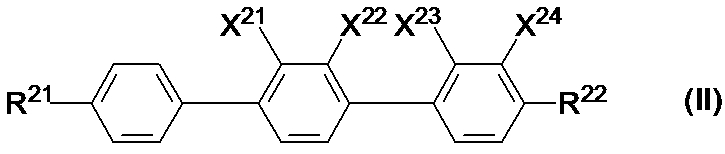
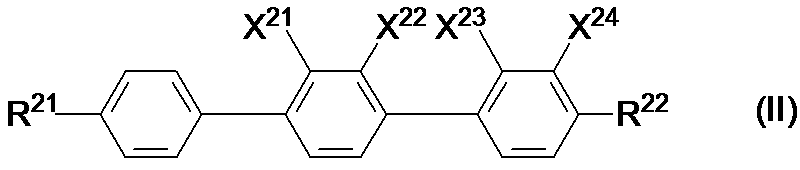
- R 21 to R 22 each independently represents an alkyl group having 1 to 10 carbon atoms or an alkenyl group having 2 to 10 carbon atoms
- X 21 to X 24 each independently represents a hydrogen atom or fluorine.
- a nematic liquid crystal composition is provided, and a liquid crystal display device using the liquid crystal composition is further provided.
- the liquid crystal composition having a negative ⁇ of the present invention can obtain a significantly low viscosity, has good solubility at low temperatures, and has a very small change in specific resistance and voltage holding ratio due to heat and light.
- the VA type and PSVA type liquid crystal display elements using this are very useful because they can achieve high-speed response and display defects are suppressed.
- R 11 to R 13 represent an alkyl group or an alkoxy group having 1 to 22 carbon atoms, preferably an alkyl group or an alkoxy group having 1 to 10 carbon atoms, and 1 to 5 carbon atoms. Of these, an alkyl group or an alkyl group is more preferable.
- the compounds represented by the general formulas (I-1) to (I-3) when importance is attached to the solubility in the liquid crystal composition, the compound represented by the general formula (I-1) is preferable. When importance is attached to the stability of a product to heat and light, a compound represented by formula (I-3) is preferred.
- the compound represented by the general formulas (I-1) to (I-3) preferably contains one or two compounds, and more preferably contains one to five compounds.
- the content is 0.001 to 1% by mass, more preferably 0.001 to 0.1% by mass, and particularly preferably 0.001 to 0.05% by mass.
- R 21 to R 22 each independently represents an alkyl group having 1 to 10 carbon atoms or an alkenyl group having 2 to 10 carbon atoms.
- X 21 to X 24 each independently represent a hydrogen atom or a fluorine atom, but at least one is preferably a fluorine atom.
- the compound represented by the general formula (II) is preferably a compound represented by the following general formula (II-a) to general formula (II-f).
- R 21 to R 22 each independently represents an alkyl group having 1 to 10 carbon atoms or an alkenyl group having 2 to 10 carbon atoms.
- general formula (II-a) to general formula (II-f) are more preferable.
- the present invention contains at least one compound represented by the general formula (II), preferably 1 to 10 compounds, particularly preferably 1 to 5 compounds, and its content is 5 To 30% by mass, and more preferably 5 to 20% by mass.
- the liquid crystal composition of the present invention further has a general formula (III) as a third component.
- R 31 to R 32 each independently represents an alkyl group having 1 to 10 carbon atoms, an alkoxy group, or an alkenyl group having 2 to 10 carbon atoms.
- M 31 is preferably a trans-1,4-cyclohexylene group or a 1,4-phenylene group.
- n 31 represents 0 or 1;
- the compound represented by the general formula (III) can be contained, preferably 1 to 10 kinds, more preferably 1 to 8 kinds, particularly preferably 5 to Preferably it is 50% by weight, more preferably 5 to 30% by weight.
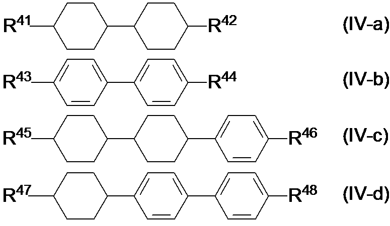
- the liquid crystal composition of the present invention may further be represented by formulas (IV-a) to (IV-d):
- the compound chosen from the compound group represented by these can be contained.
- R 41 to R 48 each independently represents an alkyl group having 1 to 10 carbon atoms, an alkoxy group, or an alkenyl group having 2 to 10 carbon atoms.
- a compound selected from the group of compounds represented by formulas (IV-a) to (IV-d) can be contained, preferably 1 to 10 types, preferably 1 to It is particularly preferable to contain 8 types, and the content is preferably 5 to 80% by mass, more preferably 10 to 70% by mass, and particularly preferably 20 to 60% by mass.
- ⁇ at 25 ° C. is ⁇ 2.0 to ⁇ 6.0, more preferably ⁇ 2.0 to ⁇ 5.5.
- ⁇ n at 25 ° C. is 0.08 to 0.14, more preferably 0.09 to 0.13, and particularly preferably 0.09 to 0.12. More specifically, it is preferably 0.10 to 0.13 when dealing with a thin cell gap, and preferably 0.08 to 0.10 when dealing with a thick cell gap.
- the ⁇ at 20 ° C. is 10 to 30 mPa ⁇ s, more preferably 10 to 25 mPa ⁇ s, and particularly preferably 10 to 22 mPa ⁇ s.
- T ni is 60 ° C. to 120 ° C., more preferably 70 ° C. to 100 ° C., and particularly preferably 70 ° C. to 85 ° C.
- the liquid crystal composition of the present invention may contain a normal nematic liquid crystal, a smectic liquid crystal, a cholesteric liquid crystal, a polymerizable monomer, etc. in addition to the above-mentioned compounds.
- the liquid crystal composition of the present invention may contain a polymerizable compound in order to produce a liquid crystal display element such as a PS mode, a PSA mode, or a PSVA mode.
- a polymerizable compound such as a PS mode, a PSA mode, or a PSVA mode.
- the polymerizable compound that can be used include a photopolymerizable monomer that undergoes polymerization by energy rays such as light.
- the structure has, for example, a liquid crystal skeleton in which a plurality of six-membered rings such as biphenyl derivatives and terphenyl derivatives are connected. Examples thereof include a polymerizable compound. More specifically, the general formula (V)
- X 51 and X 52 each independently represent a hydrogen atom or a methyl group
- Sp 1 and Sp 2 are each independently a single bond, an alkylene group having 1 to 8 carbon atoms, or —O— (CH 2 ) s —.
- Z 51 represents —OCH 2 —, —CH 2 O—, —COO—, —OCO—, —CF 2 O—, —OCF 2 —, —CH 2 CH 2 —, —CF 2 CF 2 —, —CH ⁇ CH—COO—, —CH ⁇ CH—OCO—, —COO—CH ⁇ CH—, —OCO—CH ⁇ CH—, —COO—CH 2 CH 2 —, —OCO—CH 2 CH 2 —, —CH 2 CH 2 —COO—, —CH 2 CH 2 —OCO—, —COO—CH 2 —, —OCO—CH 2 —, —CH 2 —COO—, —CH 2 CH 2 —OCO—, —COO—CH 2 —, —OCO—CH 2 —, —CH 2 —COO—, —CH 2 —OCO—, —CY 1 ⁇ CY 2 — (Wherein Y 1 and Y 2
- X 51 and X 52 are each preferably a diacrylate derivative that represents a hydrogen atom, or a dimethacrylate derivative that has a methyl group, and a compound in which one represents a hydrogen atom and the other represents a methyl group.
- diacrylate derivatives are the fastest, dimethacrylate derivatives are slow, asymmetric compounds are in the middle, and a preferred embodiment can be used depending on the application.
- a dimethacrylate derivative is particularly preferable.
- Sp 1 and Sp 2 each independently represent a single bond, an alkylene group having 1 to 8 carbon atoms or —O— (CH 2 ) s —, but at least one of them is a single bond in a PSA display element.
- a compound in which both represent a single bond or one in which one represents a single bond and the other represents an alkylene group having 1 to 8 carbon atoms or —O— (CH 2 ) s — is preferable.
- 1 to 4 alkyl groups are preferable, and s is preferably 1 to 4.
- Z 51 is —OCH 2 —, —CH 2 O—, —COO—, —OCO—, —CF 2 O—, —OCF 2 —, —CH 2 CH 2 —, —CF 2 CF 2 — or a single bond
- —COO—, —OCO— or a single bond is more preferred, and a single bond is particularly preferred.
- M 51 represents a 1,4-phenylene group, a trans-1,4-cyclohexylene group or a single bond in which any hydrogen atom may be substituted by a fluorine atom. preferable.
- C represents a ring structure other than a single bond
- Z 51 is preferably a linking group other than a single bond.
- M 51 is a single bond
- Z 51 is preferably a single bond.
- the ring structure between Sp 1 and Sp 2 is specifically preferably the structure described below.
- both ends shall be bonded to Sp 1 or Sp 2.
- the polymerizable compounds containing these skeletons are optimal for PSA-type liquid crystal display elements because of the alignment regulating power after polymerization, and a good alignment state can be obtained, so that display unevenness is suppressed or does not occur at all.
- general formula (V-1) to general formula (V-4) are particularly preferable, and general formula (V-2) is most preferable.
- the polymerization proceeds even when no polymerization initiator is present, but may contain a polymerization initiator in order to accelerate the polymerization.
- the polymerization initiator include benzoin ethers, benzophenones, acetophenones, benzyl ketals, acylphosphine oxides, and the like.
- the liquid crystal composition containing the polymerizable compound of the present invention is provided with liquid crystal alignment ability by polymerizing the polymerizable compound contained therein by ultraviolet irradiation, and transmits light through the birefringence of the liquid crystal composition. It is used in a liquid crystal display element that controls As liquid crystal display elements, AM-LCD (active matrix liquid crystal display element), TN (nematic liquid crystal display element), STN-LCD (super twisted nematic liquid crystal display element), OCB-LCD and IPS-LCD (in-plane switching liquid crystal display element) However, it is particularly useful for AM-LCDs and can be used for transmissive or reflective liquid crystal display elements.
- the two substrates of the liquid crystal cell used in the liquid crystal display element can be made of a transparent material having flexibility such as glass or plastic, and one of them can be an opaque material such as silicon.
- a transparent substrate having a transparent electrode layer can be obtained, for example, by sputtering indium tin oxide (ITO) on a transparent substrate such as a glass plate.
- the color filter can be prepared by, for example, a pigment dispersion method, a printing method, an electrodeposition method, or a dyeing method.
- a method for producing a color filter by a pigment dispersion method will be described as an example.
- a curable coloring composition for a color filter is applied on the transparent substrate, subjected to patterning treatment, and cured by heating or light irradiation. By performing this process for each of the three colors red, green, and blue, a pixel portion for a color filter can be created.
- a pixel electrode provided with an active element such as a TFT, a thin film diode, or a metal insulator metal specific resistance element may be provided on the substrate.
- the substrate is opposed so that the transparent electrode layer is on the inside.
- the thickness of the obtained light control layer is 1 to 100 ⁇ m. More preferably, the thickness is 1.5 to 10 ⁇ m.
- the polarizing plate it is preferable to adjust the product of the refractive index anisotropy ⁇ n of the liquid crystal and the cell thickness d so that the contrast is maximized.
- the polarizing axis of each polarizing plate can be adjusted so that the viewing angle and contrast are good.
- a retardation film for widening the viewing angle can also be used.
- the spacer examples include glass particles, plastic particles, alumina particles, and a photoresist material.
- a sealant such as an epoxy thermosetting composition is screen-printed on the substrates with a liquid crystal inlet provided, the substrates are bonded together, and heated to thermally cure the sealant.
- a normal vacuum injection method or an ODF method can be used as a method of sandwiching the polymerizable compound-containing liquid crystal composition between two substrates. Although it has the subject which remains after, in this invention, it can use suitably by the display element manufactured using ODF method.
- an appropriate polymerization rate is desirable in order to obtain good alignment performance of liquid crystals. Therefore, active energy rays such as ultraviolet rays or electron beams are irradiated singly or in combination or sequentially.
- the method of polymerizing by is preferred.
- ultraviolet rays When ultraviolet rays are used, a polarized light source or a non-polarized light source may be used.
- the polymerization is performed in a state where the polymerizable compound-containing liquid crystal composition is sandwiched between two substrates, at least the substrate on the irradiation surface side must be given appropriate transparency to the active energy rays. I must.
- the orientation state of the unpolymerized part is changed by changing conditions such as an electric field, a magnetic field, or temperature, and further irradiation with active energy rays is performed. Then, it is possible to use a means for polymerization.
- a means for polymerization In particular, when ultraviolet exposure is performed, it is preferable to perform ultraviolet exposure while applying an alternating electric field to the polymerizable compound-containing liquid crystal composition.
- the alternating electric field to be applied is preferably an alternating current having a frequency of 10 Hz to 10 kHz, more preferably a frequency of 60 Hz to 10 kHz, and the voltage is selected depending on a desired pretilt angle of the liquid crystal display element. That is, the pretilt angle of the liquid crystal display element can be controlled by the applied voltage. In the MVA mode liquid crystal display element, the pretilt angle is preferably controlled from 80 degrees to 89.9 degrees from the viewpoint of alignment stability and contrast.
- the temperature during irradiation is preferably within a temperature range in which the liquid crystal state of the liquid crystal composition of the present invention is maintained. Polymerization is preferably performed at a temperature close to room temperature, that is, typically at a temperature of 15 to 35 ° C.
- a lamp for generating ultraviolet rays a metal halide lamp, a high-pressure mercury lamp, an ultra-high pressure mercury lamp, or the like can be used.
- a wavelength of the ultraviolet-rays to irradiate it is preferable to irradiate the ultraviolet-ray of the wavelength range which is not the absorption wavelength range of a liquid crystal composition, and it is preferable to cut and use an ultraviolet-ray as needed.
- Intensity of ultraviolet irradiation is preferably from 0.1mW / cm 2 ⁇ 100W / cm 2, 2mW / cm 2 ⁇ 50W / cm 2 is more preferable.
- the amount of energy of ultraviolet rays to be irradiated can be adjusted as appropriate, but is preferably 10 mJ / cm 2 to 500 J / cm 2, and more preferably 100 mJ / cm 2 to 200 J / cm 2 .
- the intensity may be changed.
- the time for irradiating with ultraviolet rays is appropriately selected depending on the intensity of the irradiated ultraviolet rays, but is preferably from 10 seconds to 3600 seconds, and more preferably from 10 seconds to 600 seconds.
- the liquid crystal display device using the liquid crystal composition of the present invention is useful for achieving both high-speed response and suppression of display failure, and is particularly useful for a liquid crystal display device for active matrix driving, including VA mode, PSVA mode, It can be applied to PSA mode, IPS mode or ECB mode liquid crystal display elements.
- the measured characteristics are as follows.
- T ni Nematic phase-isotropic liquid phase transition temperature (° C.) ⁇ n: refractive index anisotropy at 25 ° C. ⁇ : dielectric anisotropy at 25 ° C. ⁇ : viscosity at 20 ° C. (mPa ⁇ s) ⁇ 1: rotational viscosity at 25 ° C. (mPa ⁇ s) VHR: Voltage holding ratio (%) at 60 ° C. under conditions of frequency 60 Hz and applied voltage 1 V Burn-in: The burn-in evaluation of the liquid crystal display element is based on the following four-level evaluation of the afterimage level of the fixed pattern when the predetermined fixed pattern is displayed in the display area for 1000 hours and then the entire screen is uniformly displayed. went.
- Example 1 A liquid crystal composition LC-1 shown below was prepared.
- the physical properties of the liquid crystal composition LC-1 were as follows.
- a liquid crystal composition LCM-1 was prepared by adding 0.03% of a compound represented by the formula: The physical property value was almost the same as LC-1.
- the initial VHR of the liquid crystal composition LCM-1 was 98.4%, whereas the VHR after standing at 150 ° C. for 1 hour at a high temperature was 98.2%.
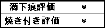
- a VA liquid crystal display device was produced using the liquid crystal composition LCM-1, and the image sticking and the drop mark were measured by the above-described method. As a result, the following excellent results were shown.
- Example 1 The initial VHR of the liquid crystal composition LC-1 to which the compound represented by the formula (I-1-1) described in Example 1 was not added was 98.5%, while 1 at 150 ° C. The VHR after standing at high temperature for 8 hours was 86.1%, which was significantly lower than the initial value. Further, a VA liquid crystal display element was produced using the liquid crystal composition LC-1, and the image sticking and the dropping trace were measured by the above-described method. As a result, the results were inferior to those of Example 1 as shown below.
- the physical properties of the liquid crystal composition LC-2 were as follows.
- Liquid crystal composition LCM-2 was prepared by adding 0.03% of the compound represented by formula (I-1-1) to 99.97% of liquid crystal composition LC-2. Its physical property value was almost the same as LC-2.
- the liquid crystal composition LC-2 not containing the compound represented by the general formula (II) has a viscosity ⁇ and a rotational viscosity ⁇ 1 compared to the liquid crystal composition LCM-1 containing the compound represented by the general formula (II). It was shown that the value significantly increased to about 10%.
- the initial VHR of the liquid crystal composition LCM-2 was 98.3%, whereas the VHR after standing at high temperature for 1 hour at 150 ° C. was 97.4%.
- a VA liquid crystal display element was prepared using the liquid crystal composition LCM-2, and the image sticking and the drop mark were measured by the above-described method. As a result, the results were inferior to those of Example 1 as shown below.
- Example 2 As a result of measuring the response speed using a cell with ITO coated with a polyimide alignment film that induces homeotropic alignment with a cell gap of 3.5 ⁇ m, the response speed is 5.3 ms, which is compared with LCM-1 described in Example 1. It was inferior.
- Example 2 to Example 4 The following liquid crystal compositions LC-3 to LC-5 were prepared and their physical properties were measured. The results are shown in the following table.
- Example 5 Example 5 to Example 7.
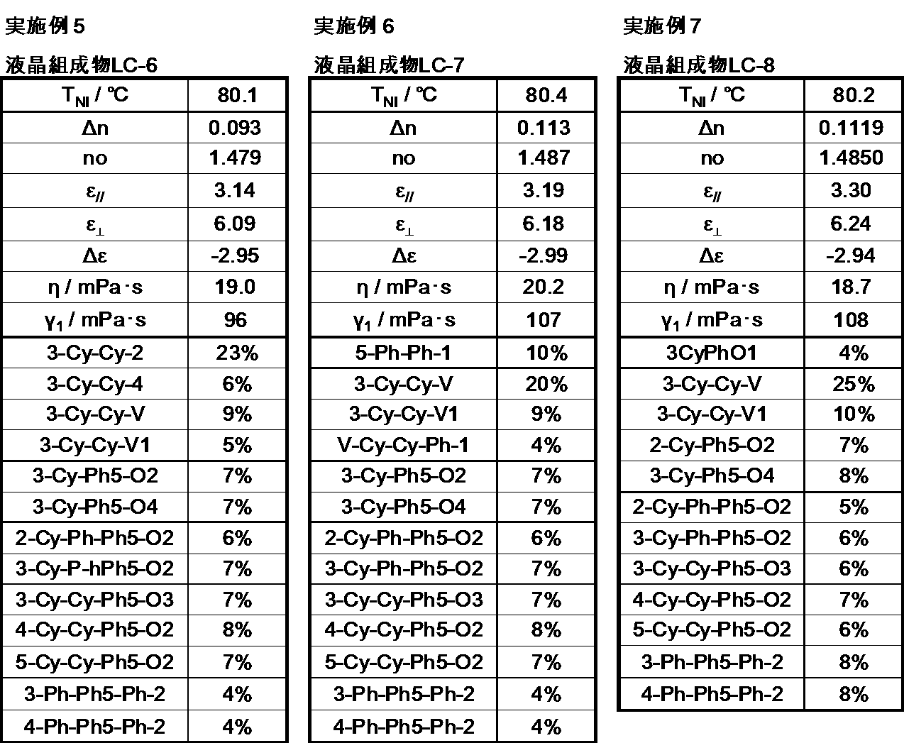
- the following liquid crystal compositions LC-6 to LC-8 were prepared and their physical properties were measured. The results are shown in the following table.
- the liquid crystal compositions LCM-6 to LCM- were prepared by adding 0.03% of the compound represented by formula (I-1-1) to 99.97% of each of the liquid crystal compositions LC-6 to LC-8. 8 were each prepared.
- the physical property values were almost the same as before the addition.
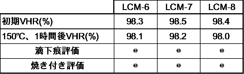
- the initial VHR of the liquid crystal compositions LCM-6 to LCM-8 and the VHR after standing at 150 ° C. for 1 hour were almost unchanged. Further, when the burn-in and dropping traces of the VA liquid crystal display devices manufactured using the liquid crystal compositions LCM-6 to LCM-8 were measured, the following excellent results were shown.
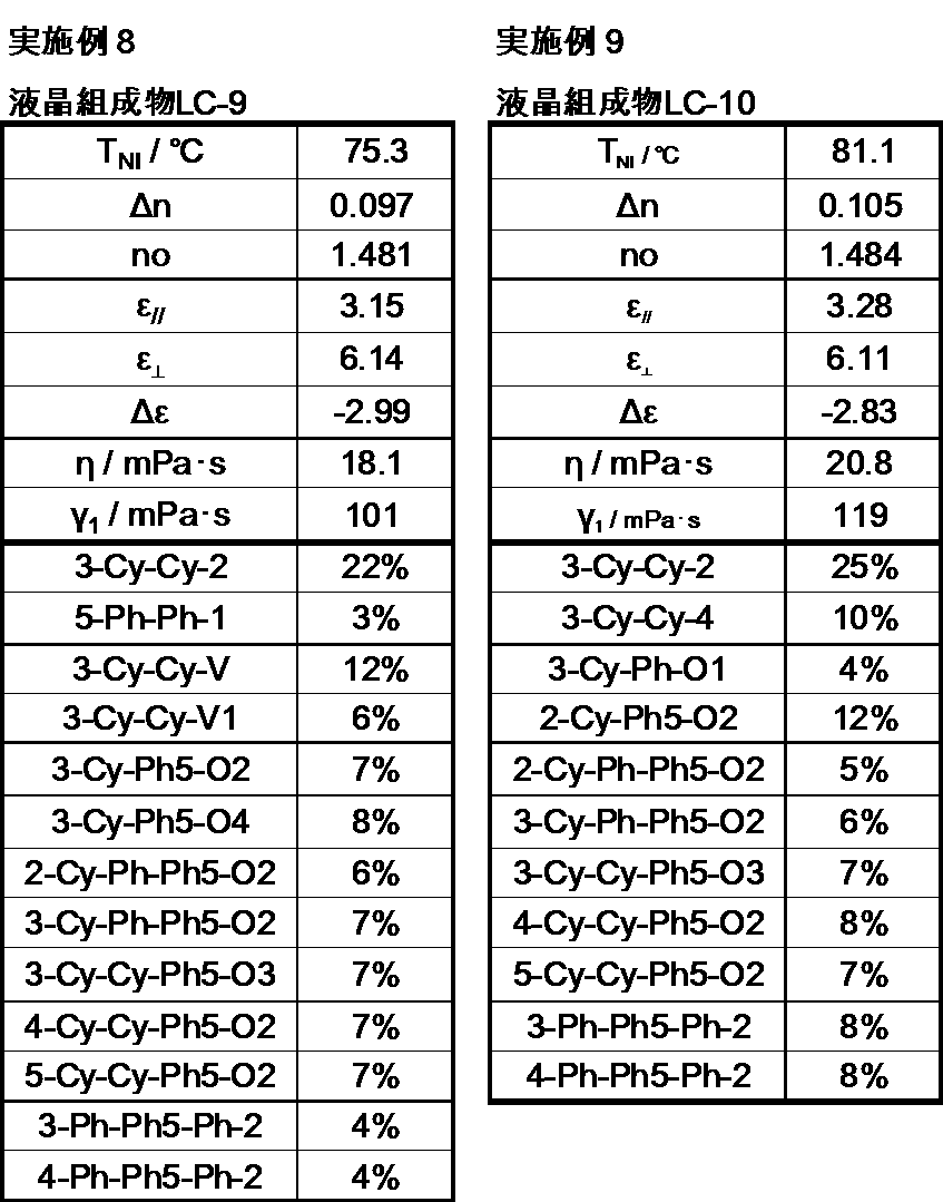
- Example 8 The following liquid crystal compositions LC-9 and LC-10 were prepared and their physical properties were measured. The results are shown in the following table.
- the liquid crystal compositions LCM-9 and LCM-10 were prepared by adding 0.03% of the compound represented by formula (I).
- the physical property values were almost the same as before the addition.
- the initial VHR of the liquid crystal compositions LCM-9 and LCM-10 and the VHR after standing at high temperature for 1 hour at 150 ° C. were almost unchanged. Further, when the burn-in and drop marks were measured on the VA liquid crystal display device produced using the liquid crystal compositions LCM-9 and LCM-10, the following excellent results were shown.
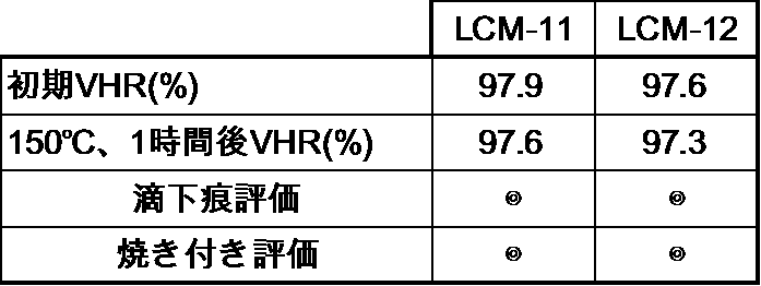
- the liquid crystal compositions LCM-11 and LCM-12 were respectively prepared by adding 0.03% of the compound represented by formula (II).
- the physical property values were almost the same as before the addition.
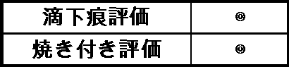
- the initial VHR of the liquid crystal compositions LCM-11 and LCM-12 and the VHR after standing at high temperature for 1 hour at 150 ° C. were almost unchanged. Further, when the burn-in and dropping traces of the VA liquid crystal display device manufactured using the liquid crystal compositions LCM-10 and LCM-11 were measured, the following excellent results were shown.
- Example 12 With respect to 99.7% of the liquid crystal composition LCM-1 described in Example 1,
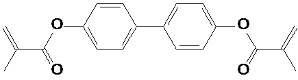
- a polymerizable liquid crystal composition CLCM-1 is prepared by adding 0.3% of a polymerizable compound represented by formula (II) and uniformly dissolving, and inducing homeotropic alignment with a cell gap of 3.5 ⁇ m. It inject
- a polymerizable liquid crystal composition CLCM-2 and CLCM-3 were respectively prepared by adding 0.3% of a polymerizable compound represented by formula (II) and uniformly dissolving, and the polymerizable liquid crystal composition was prepared with a cell gap of 3.5 ⁇ m. It injected by the vacuum injection method to the cell with ITO which apply
- Example 13 to Example 15 With respect to 99.7% of each of the liquid crystal compositions LCM-6, LCM-7 and LCM-8 described in Example 5, Example 6 and Example 7,
- a polymerizable liquid crystal composition CLCM-4, CLCM-5 and CLCM-6 were prepared by adding 0.3% of a polymerizable compound represented by the formula (1) and uniformly dissolving, respectively. It injected by the vacuum injection method to the cell with ITO which apply
Landscapes
- Chemical & Material Sciences (AREA)
- Physics & Mathematics (AREA)
- Crystallography & Structural Chemistry (AREA)
- Engineering & Computer Science (AREA)
- Materials Engineering (AREA)
- Organic Chemistry (AREA)
- Nonlinear Science (AREA)
- Mathematical Physics (AREA)
- General Physics & Mathematics (AREA)
- Optics & Photonics (AREA)
- Dispersion Chemistry (AREA)
- Microelectronics & Electronic Packaging (AREA)
- Liquid Crystal Substances (AREA)
Abstract
Description
第一成分として、一般式(I-1)から一般式(I-3)

第二成分として、一般式(II)

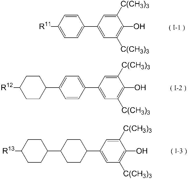
一般式(I-1)から一般式(I-3)で表される化合物中、液晶組成物に対する溶解性を重視した場合は一般式(I-1)で表される化合物が好ましく、液晶組成物の熱や光に対する安定性を重視した場合は一般式(I-3)で表される化合物が好ましい。
本願発明の液晶組成物において、一般式(I-1)から一般式(I-3)で表される化合物を1種又は2種を含有するが好ましく、1種から5種含有することが更に好ましく、その含有量は0.001から1質量%であることが好ましく、0.001から0.1質量%が更に好ましく、0.001から0.05質量%が特に好ましい。
第二成分として使用する一般式(II)
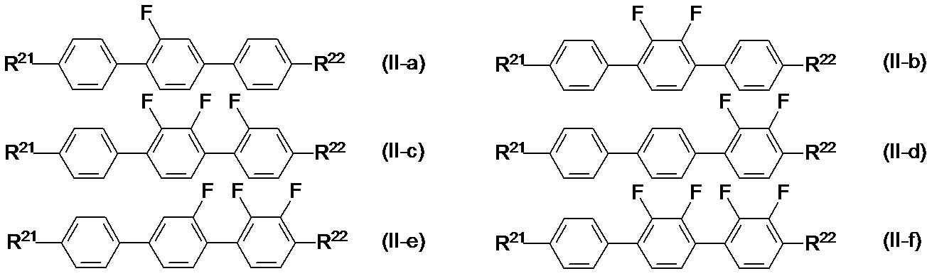
一般式(II-a)から一般式(II-f)で表される化合物中、一般式(II-a)、一般式(II-b)及び一般式(II-d)が更に好ましい。

一般式(III)で表される化合物において、R31~R32はお互い独立しては炭素原子数1から10のアルキル基、アルコキシ基、又は炭素原子数2から10のアルケニル基を表す。M31はトランス-1,4-シクロへキシレン基又は1,4-フェニレン基であることが好ましい。n31は0又は1を表す。
本願発明の液晶組成物は、また更に、一般式(IV-a)から一般式(IV-d)
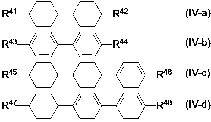
(式中、R41~R48はお互い独立しては炭素原子数1から10のアルキル基、アルコキシ基又は炭素原子数2から10のアルケニル基を表す。)
本願発明では一般式(IV-a)から一般式(IV-d)で表される化合物群から選ばれる化合物を含有することができるが、1種~10種含有することが好ましく、1種~8種含有することが特に好ましく、その含有量は5から80質量%であることが好ましく、10から70質量%であることが更に好ましく、20から60質量%であることが特に好ましい。

(式中、X51及びX52はそれぞれ独立して、水素原子又はメチル基を表し、
Sp1及びSp2はそれぞれ独立して、単結合、炭素原子数1~8のアルキレン基又は-O-(CH2)s-
(式中、sは2から7の整数を表し、酸素原子は芳香環に結合するものとする。)を表し、
Z51は-OCH2-、-CH2O-、-COO-、-OCO-、-CF2O-、-OCF2-、-CH2CH2-、-CF2CF2-、-CH=CH-COO-、-CH=CH-OCO-、-COO-CH=CH-、-OCO-CH=CH-、-COO-CH2CH2-、-OCO-CH2CH2-、-CH2CH2-COO-、-CH2CH2-OCO-、-COO-CH2-、-OCO-CH2-、-CH2-COO-、-CH2-OCO-、-CY1=CY2-(式中、Y1及びY2はそれぞれ独立して、フッ素原子又は水素原子を表す。)、-C≡C-又は単結合を表し、
M51は1,4-フェニレン基、トランス-1,4-シクロヘキシレン基又は単結合を表し、式中の全ての1,4-フェニレン基は、任意の水素原子がフッ素原子により置換されていても良い。)で表される二官能モノマーが好ましい。

これらの骨格を含む重合性化合物は重合後の配向規制力がPSA型液晶表示素子に最適であり、良好な配向状態が得られることから、表示ムラが抑制されるか、又は、全く発生しない。
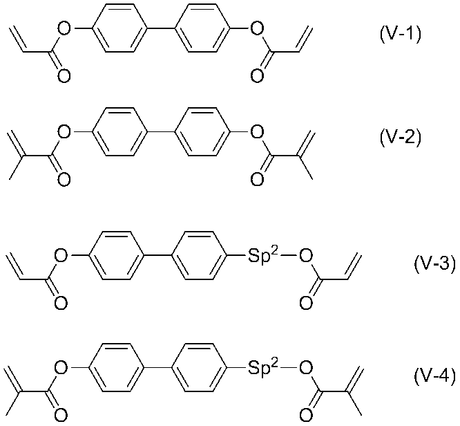
本発明の液晶組成物にモノマーを添加する場合において、重合開始剤が存在しない場合でも重合は進行するが、重合を促進するために重合開始剤を含有していてもよい。重合開始剤としては、ベンゾインエーテル類、ベンゾフェノン類、アセトフェノン類、ベンジルケタール類、アシルフォスフィンオキサイド類等が挙げられる。
Δn :25℃における屈折率異方性
Δε :25℃における誘電率異方性
η :20℃における粘度(mPa・s)
γ1 :25℃における回転粘性(mPa・s)
VHR:周波数60Hz,印加電圧1Vの条件下で60℃における電圧保持率(%)
焼き付き:
液晶表示素子の焼き付き評価は、表示エリア内に所定の固定パターンを1000時間表示させた後に、全画面均一な表示を行ったときの固定パターンの残像のレベルを目視にて以下の4段階評価で行った。
○残像ごく僅かに有るも許容できるレベル
△残像有り許容できないレベル
×残像有りかなり劣悪
滴下痕 :
液晶表示装置の滴下痕の評価は、全面黒表示した場合における白く浮かび上がる滴下痕を目視にて以下の4段階評価で行った。
○残像ごく僅かに有るも許容できるレベル
△残像有り許容できないレベル
×残像有りかなり劣悪
尚、実施例において化合物の記載について以下の略号を用いる。
(側鎖)
-n -CnH2n+1 炭素原子数nの直鎖状アルキル基
n- CnH2n+1- 炭素原子数nの直鎖状アルキル基
-On -OCnH2n+1 炭素原子数nの直鎖状アルコキシ基
-V -CH=CH2
V- CH2=CH-
-V1 -CH=CH-CH3
(環構造)

以下に示される液晶組成物LC-1を調製した。
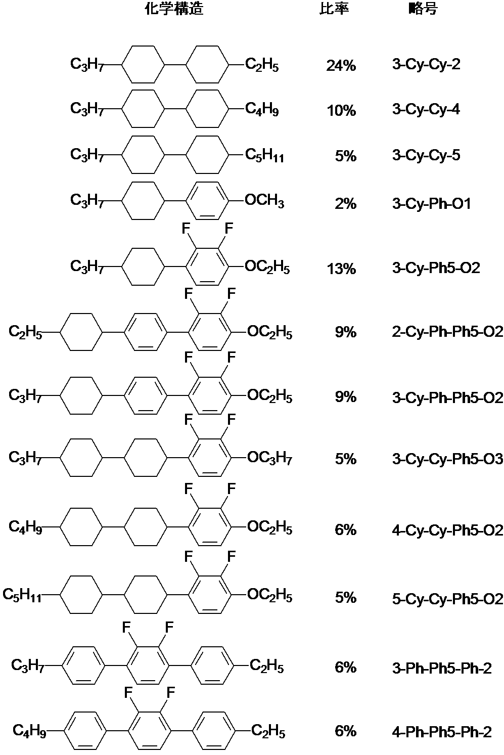
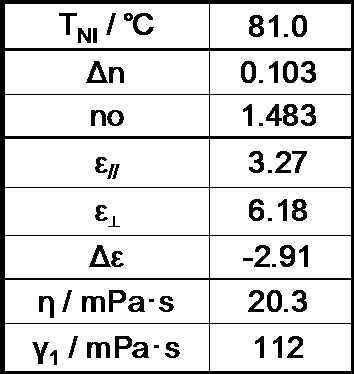
液晶組成物LC-1 99.97%に式(I-1-1)

(比較例1)
実施例1に記載の式(I-1-1)で表される化合物を添加していない液晶組成物LC-1の初期のVHRは98.5%であったのに対し、150℃で1時間の高温放置後のVHRは、86.1%と初期に対して大きく低下した。
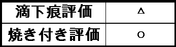
また、液晶組成物LC-1を用いてVA液晶表示素子を作製し、前述の方法により焼き付き及び滴下痕の測定したところ、以下に示すように実施例1と比べて劣る結果を示した。

一般式(II)で表される化合物を含有しない、以下に示される液晶組成物LC-2を調製した。


また、液晶組成物LCM-2を用いてVA液晶表示素子を作製し、前述の方法により焼き付き及び滴下痕の測定したところ、以下に示すように実施例1に比べて劣る結果を示した。
(実施例2から実施例4)
次に示す液晶組成物LC-3~LC-5を調製し、その物性値を測定した。この結果を次の表に示す。

液晶組成物LCM-3~LCM-5の初期のVHR及び150℃で1時間の高温放置後のVHRはほとんど変化がなかった。また、液晶組成物LCM-3~LCM-5を用いて作製したVA液晶表示素子の焼き付き及び滴下痕の測定したところ、以下に示すように優れた結果を示した。

次に示す液晶組成物LC-6~LC-8を調製し、その物性値を測定した。この結果を次の表に示す。
液晶組成物LCM-6~LCM-8の初期のVHR及び150℃で1時間の高温放置後のVHRはほとんど変化がなかった。また、液晶組成物LCM-6~LCM-8を用いて作製したVA液晶表示素子の焼き付き及び滴下痕の測定したところ、以下に示すように優れた結果を示した。
次に示す液晶組成物LC-9及びLC-10を調製し、その物性値を測定した。この結果を次の表に示す。

液晶組成物LCM-9及びLCM-10の初期のVHR及び150℃で1時間の高温放置後のVHRはほとんど変化がなかった。また、液晶組成物LCM-9及びLCM-10を用いて作製したVA液晶表示素子の焼き付き及び滴下痕の測定したところ、以下に示すように優れた結果を示した。

上記の液晶組成物LC-9及びLC-10の各々99.97%に対して、式(I-2-1)
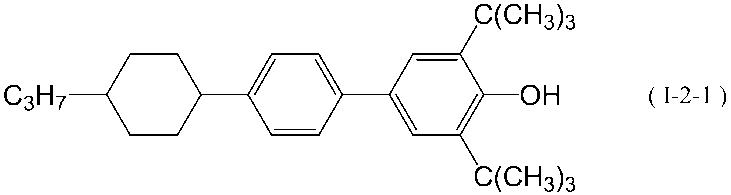
液晶組成物LCM-11及びLCM-12の初期のVHR及び150℃で1時間の高温放置後のVHRはほとんど変化がなかった。また、液晶組成物LCM-10及びLCM-11を用いて作製したVA液晶表示素子の焼き付き及び滴下痕の測定したところ、以下に示すように優れた結果を示した。
実施例1に記載の液晶組成物LCM-1 99.7%に対して、

比較例1で使用した液晶組成物LC-1及び比較例2で使用した液晶組成物LCM-2各々99.7%に対して、
本液晶表示素子の焼き付き及び滴下痕の測定したところ、以下に示すように実施例10に比べて劣る結果を示した。

実施例5、実施例6及び実施例7に記載の液晶組成物LCM-6、LCM-7及びLCM-8の各々99.7%に対して、


Claims (7)
- 第一成分として、一般式(I-1)から一般式(I-3)

第二成分として、一般式(II)
- 第三成分として、一般式(III)

で表される化合物を一種又は二種以上含有する請求項1記載のネマチック液晶組成物。 - 更に、一般式(IV-a)から一般式(IV-d)
- 一般式(I-1)から一般式(I-3)で表される化合物からなる群から選ばれる化合物の含有量が0.001質量%から1質量%であり、一般式(II)で表される化合物の含有量が5質量%から30質量%である請求項1から3のいずれか一項に記載のネマチック液晶組成物。
- 一般式(V)

Sp1及びSp2はそれぞれ独立して、単結合、炭素原子数1~8のアルキレン基又は-O-(CH2)s-
(式中、sは2から7の整数を表し、酸素原子は芳香環に結合するものとする。)を表し、
Z51は-OCH2-、-CH2O-、-COO-、-OCO-、-CF2O-、-OCF2-、-CH2CH2-、-CF2CF2-、-CH=CH-COO-、-CH=CH-OCO-、-COO-CH=CH-、-OCO-CH=CH-、-COO-CH2CH2-、-OCO-CH2CH2-、-CH2CH2-COO-、-CH2CH2-OCO-、-COO-CH2-、-OCO-CH2-、-CH2-COO-、-CH2-OCO-、-CY1=CY2-(式中、Y1及びY2はそれぞれ独立して、フッ素原子又は水素原子を表す。)、-C≡C-又は単結合を表し、
M51は1,4-フェニレン基、トランス-1,4-シクロヘキシレン基又は単結合を表し、式中の全ての1,4-フェニレン基は、任意の水素原子がフッ素原子により置換されていても良い。)で表される重合性化合物を含有する請求項1から4のいずれか一項に記載のネマチック液晶組成物。 - 透明導電性材料からなる共通電極を具備した第一の基板と、透明導電性材料からなる画素電極と各画素に具備した画素電極を制御する薄膜トランジスターを具備した第二の基板と、前記第一の基板と第二の基板間に挟持された液晶組成物を有し、該液晶組成物中の液晶分子の電圧無印加時の配向が前記基板に対して略垂直である液晶表示素子であって、該液晶組成物として請求項1から5のいずれか一項に記載のネマチック液晶組成物を用いた液晶表示素子。
- 請求項5に記載の重合性化合物を含有するネマチック液晶組成物を用い、電圧印加下あるいは電圧無印加下で該液晶組成物中に含有する重合性化合物を重合させて作製した高分子安定化モード液晶表示素子。
Priority Applications (2)
| Application Number | Priority Date | Filing Date | Title |
|---|---|---|---|
| JP2014510322A JP5582272B1 (ja) | 2012-11-08 | 2013-11-06 | ネマチック液晶組成物及びこれを用いた液晶表示素子 |
| US14/440,410 US9411207B2 (en) | 2012-11-08 | 2013-11-06 | Nematic liquid crystal composition and liquid crystal display element using the same |
Applications Claiming Priority (2)
| Application Number | Priority Date | Filing Date | Title |
|---|---|---|---|
| JP2012-246316 | 2012-11-08 | ||
| JP2012246316 | 2012-11-08 |
Publications (1)
| Publication Number | Publication Date |
|---|---|
| WO2014073572A1 true WO2014073572A1 (ja) | 2014-05-15 |
Family
ID=50684674
Family Applications (1)
| Application Number | Title | Priority Date | Filing Date |
|---|---|---|---|
| PCT/JP2013/080023 Ceased WO2014073572A1 (ja) | 2012-11-08 | 2013-11-06 | ネマチック液晶組成物及びこれを用いた液晶表示素子 |
Country Status (4)
| Country | Link |
|---|---|
| US (1) | US9411207B2 (ja) |
| JP (1) | JP5582272B1 (ja) |
| TW (1) | TWI597352B (ja) |
| WO (1) | WO2014073572A1 (ja) |
Cited By (1)
| Publication number | Priority date | Publication date | Assignee | Title |
|---|---|---|---|---|
| JP2015120907A (ja) * | 2013-12-16 | 2015-07-02 | メルク パテント ゲゼルシャフト ミット ベシュレンクテル ハフツングMerck Patent Gesellschaft mit beschraenkter Haftung | 液晶媒体 |
Families Citing this family (2)
| Publication number | Priority date | Publication date | Assignee | Title |
|---|---|---|---|---|
| WO2014136315A1 (ja) | 2013-03-06 | 2014-09-12 | Dic株式会社 | ネマチック液晶組成物及びこれを用いた液晶表示素子 |
| TWI623609B (zh) * | 2013-03-06 | 2018-05-11 | Dainippon Ink & Chemicals | Nematic liquid crystal composition and liquid crystal display element using same |
Citations (4)
| Publication number | Priority date | Publication date | Assignee | Title |
|---|---|---|---|---|
| JPH09124529A (ja) * | 1995-10-20 | 1997-05-13 | Merck Patent Gmbh | 2,6−ジ−tert−ブチルフェノール化合物 |
| DE10117224A1 (de) * | 2000-04-19 | 2002-02-21 | Merck Patent Gmbh | Verfahren zur Stabilisierung von Halogenaromaten |
| JP2006502205A (ja) * | 2002-10-07 | 2006-01-19 | メルク パテント ゲゼルシャフト ミット ベシュレンクテル ハフトング | キラルなフェノール誘導体、それらを含む液晶媒体 |
| JP2010256904A (ja) * | 2009-04-23 | 2010-11-11 | Merck Patent Gmbh | 液晶ディスプレイ |
Family Cites Families (7)
| Publication number | Priority date | Publication date | Assignee | Title |
|---|---|---|---|---|
| JPH06235925A (ja) | 1993-02-10 | 1994-08-23 | Matsushita Electric Ind Co Ltd | 液晶表示素子の製造方法 |
| US6380555B1 (en) | 1999-12-24 | 2002-04-30 | Micron Technology, Inc. | Bumped semiconductor component having test pads, and method and system for testing bumped semiconductor components |
| US6977704B2 (en) | 2001-03-30 | 2005-12-20 | Fujitsu Display Technologies Corporation | Liquid crystal display |
| DE10216197B4 (de) | 2002-04-12 | 2013-02-07 | Merck Patent Gmbh | Flüssigkristallmedium und und seine Verwendung in einer elektrooptischen Anzeige |
| JP2006169472A (ja) | 2004-12-20 | 2006-06-29 | Chisso Corp | 液晶組成物および液晶表示素子 |
| CN101351432B (zh) | 2006-01-06 | 2011-08-31 | 智索株式会社 | 具有烯基的单氟化联三苯化合物、液晶组成物及液晶显示元件 |
| WO2013161096A1 (ja) * | 2012-04-26 | 2013-10-31 | Dic株式会社 | ネマチック液晶組成物及びこれを用いた液晶表示素子 |
-
2013
- 2013-10-30 TW TW102139216A patent/TWI597352B/zh active
- 2013-11-06 JP JP2014510322A patent/JP5582272B1/ja active Active
- 2013-11-06 WO PCT/JP2013/080023 patent/WO2014073572A1/ja not_active Ceased
- 2013-11-06 US US14/440,410 patent/US9411207B2/en active Active
Patent Citations (4)
| Publication number | Priority date | Publication date | Assignee | Title |
|---|---|---|---|---|
| JPH09124529A (ja) * | 1995-10-20 | 1997-05-13 | Merck Patent Gmbh | 2,6−ジ−tert−ブチルフェノール化合物 |
| DE10117224A1 (de) * | 2000-04-19 | 2002-02-21 | Merck Patent Gmbh | Verfahren zur Stabilisierung von Halogenaromaten |
| JP2006502205A (ja) * | 2002-10-07 | 2006-01-19 | メルク パテント ゲゼルシャフト ミット ベシュレンクテル ハフトング | キラルなフェノール誘導体、それらを含む液晶媒体 |
| JP2010256904A (ja) * | 2009-04-23 | 2010-11-11 | Merck Patent Gmbh | 液晶ディスプレイ |
Cited By (1)
| Publication number | Priority date | Publication date | Assignee | Title |
|---|---|---|---|---|
| JP2015120907A (ja) * | 2013-12-16 | 2015-07-02 | メルク パテント ゲゼルシャフト ミット ベシュレンクテル ハフツングMerck Patent Gesellschaft mit beschraenkter Haftung | 液晶媒体 |
Also Published As
| Publication number | Publication date |
|---|---|
| JPWO2014073572A1 (ja) | 2016-09-08 |
| US9411207B2 (en) | 2016-08-09 |
| TWI597352B (zh) | 2017-09-01 |
| JP5582272B1 (ja) | 2014-09-03 |
| TW201422784A (zh) | 2014-06-16 |
| US20150286081A1 (en) | 2015-10-08 |
Similar Documents
| Publication | Publication Date | Title |
|---|---|---|
| JP6760340B2 (ja) | ネマチック液晶組成物及びこれを用いた液晶表示素子 | |
| JP5170603B1 (ja) | ネマチック液晶組成物及びこれを用いた液晶表示素子 | |
| JP5561570B2 (ja) | ネマチック液晶組成物及びこれを用いた液晶表示素子 | |
| JP5170602B1 (ja) | ネマチック液晶組成物及びこれを用いた液晶表示素子 | |
| JP5288224B1 (ja) | 液晶組成物 | |
| JP5828906B2 (ja) | 液晶組成物及びそれを使用した液晶表示素子 | |
| JP5565542B1 (ja) | ネマチック液晶組成物及びこれを用いた液晶表示素子 | |
| JP5582272B1 (ja) | ネマチック液晶組成物及びこれを用いた液晶表示素子 | |
| WO2014125616A1 (ja) | 液晶組成物及びそれを使用した液晶表示素子 |
Legal Events
| Date | Code | Title | Description |
|---|---|---|---|
| ENP | Entry into the national phase |
Ref document number: 2014510322 Country of ref document: JP Kind code of ref document: A |
|
| 121 | Ep: the epo has been informed by wipo that ep was designated in this application |
Ref document number: 13853893 Country of ref document: EP Kind code of ref document: A1 |
|
| WWE | Wipo information: entry into national phase |
Ref document number: 14440410 Country of ref document: US |
|
| NENP | Non-entry into the national phase |
Ref country code: DE |
|
| 122 | Ep: pct application non-entry in european phase |
Ref document number: 13853893 Country of ref document: EP Kind code of ref document: A1 |