WO2014069157A1 - 液晶表示素子 - Google Patents
液晶表示素子 Download PDFInfo
- Publication number
- WO2014069157A1 WO2014069157A1 PCT/JP2013/077074 JP2013077074W WO2014069157A1 WO 2014069157 A1 WO2014069157 A1 WO 2014069157A1 JP 2013077074 W JP2013077074 W JP 2013077074W WO 2014069157 A1 WO2014069157 A1 WO 2014069157A1
- Authority
- WO
- WIPO (PCT)
- Prior art keywords
- liquid crystal
- angle
- substrate
- absorption axis
- crystal layer
- Prior art date
- Legal status (The legal status is an assumption and is not a legal conclusion. Google has not performed a legal analysis and makes no representation as to the accuracy of the status listed.)
- Ceased
Links
Images



Classifications
-
- G—PHYSICS
- G02—OPTICS
- G02F—OPTICAL DEVICES OR ARRANGEMENTS FOR THE CONTROL OF LIGHT BY MODIFICATION OF THE OPTICAL PROPERTIES OF THE MEDIA OF THE ELEMENTS INVOLVED THEREIN; NON-LINEAR OPTICS; FREQUENCY-CHANGING OF LIGHT; OPTICAL LOGIC ELEMENTS; OPTICAL ANALOGUE/DIGITAL CONVERTERS
- G02F1/00—Devices or arrangements for the control of the intensity, colour, phase, polarisation or direction of light arriving from an independent light source, e.g. switching, gating or modulating; Non-linear optics
- G02F1/01—Devices or arrangements for the control of the intensity, colour, phase, polarisation or direction of light arriving from an independent light source, e.g. switching, gating or modulating; Non-linear optics for the control of the intensity, phase, polarisation or colour
- G02F1/13—Devices or arrangements for the control of the intensity, colour, phase, polarisation or direction of light arriving from an independent light source, e.g. switching, gating or modulating; Non-linear optics for the control of the intensity, phase, polarisation or colour based on liquid crystals, e.g. single liquid crystal display cells
- G02F1/133—Constructional arrangements; Operation of liquid crystal cells; Circuit arrangements
- G02F1/1333—Constructional arrangements; Manufacturing methods
- G02F1/1335—Structural association of cells with optical devices, e.g. polarisers or reflectors
- G02F1/13363—Birefringent elements, e.g. for optical compensation
- G02F1/133636—Birefringent elements, e.g. for optical compensation with twisted orientation, e.g. comprising helically oriented LC-molecules or a plurality of twisted birefringent sublayers
-
- G—PHYSICS
- G02—OPTICS
- G02F—OPTICAL DEVICES OR ARRANGEMENTS FOR THE CONTROL OF LIGHT BY MODIFICATION OF THE OPTICAL PROPERTIES OF THE MEDIA OF THE ELEMENTS INVOLVED THEREIN; NON-LINEAR OPTICS; FREQUENCY-CHANGING OF LIGHT; OPTICAL LOGIC ELEMENTS; OPTICAL ANALOGUE/DIGITAL CONVERTERS
- G02F1/00—Devices or arrangements for the control of the intensity, colour, phase, polarisation or direction of light arriving from an independent light source, e.g. switching, gating or modulating; Non-linear optics
- G02F1/01—Devices or arrangements for the control of the intensity, colour, phase, polarisation or direction of light arriving from an independent light source, e.g. switching, gating or modulating; Non-linear optics for the control of the intensity, phase, polarisation or colour
- G02F1/13—Devices or arrangements for the control of the intensity, colour, phase, polarisation or direction of light arriving from an independent light source, e.g. switching, gating or modulating; Non-linear optics for the control of the intensity, phase, polarisation or colour based on liquid crystals, e.g. single liquid crystal display cells
- G02F1/137—Devices or arrangements for the control of the intensity, colour, phase, polarisation or direction of light arriving from an independent light source, e.g. switching, gating or modulating; Non-linear optics for the control of the intensity, phase, polarisation or colour based on liquid crystals, e.g. single liquid crystal display cells characterised by the electro-optical or magneto-optical effect, e.g. field-induced phase transition, orientation effect, guest-host interaction or dynamic scattering
- G02F1/139—Devices or arrangements for the control of the intensity, colour, phase, polarisation or direction of light arriving from an independent light source, e.g. switching, gating or modulating; Non-linear optics for the control of the intensity, phase, polarisation or colour based on liquid crystals, e.g. single liquid crystal display cells characterised by the electro-optical or magneto-optical effect, e.g. field-induced phase transition, orientation effect, guest-host interaction or dynamic scattering based on orientation effects in which the liquid crystal remains transparent
- G02F1/1396—Devices or arrangements for the control of the intensity, colour, phase, polarisation or direction of light arriving from an independent light source, e.g. switching, gating or modulating; Non-linear optics for the control of the intensity, phase, polarisation or colour based on liquid crystals, e.g. single liquid crystal display cells characterised by the electro-optical or magneto-optical effect, e.g. field-induced phase transition, orientation effect, guest-host interaction or dynamic scattering based on orientation effects in which the liquid crystal remains transparent the liquid crystal being selectively controlled between a twisted state and a non-twisted state, e.g. TN-LC cell
- G02F1/1397—Devices or arrangements for the control of the intensity, colour, phase, polarisation or direction of light arriving from an independent light source, e.g. switching, gating or modulating; Non-linear optics for the control of the intensity, phase, polarisation or colour based on liquid crystals, e.g. single liquid crystal display cells characterised by the electro-optical or magneto-optical effect, e.g. field-induced phase transition, orientation effect, guest-host interaction or dynamic scattering based on orientation effects in which the liquid crystal remains transparent the liquid crystal being selectively controlled between a twisted state and a non-twisted state, e.g. TN-LC cell the twist being substantially higher than 90°, e.g. STN-, SBE-, OMI-LC cells
Definitions
- the present invention relates to a liquid crystal display element, and more particularly to a super twisted nematic type liquid crystal display element provided with a twisted phase difference plate having a liquid crystalline polymer layer.
- a phase difference plate is provided.
- a liquid crystalline twisted phase difference plate tilting position with a liquid crystalline polymer layer
- a phase difference plate is used.
- Patent Document 1 As an STN type liquid crystal display element including a liquid crystal twisted phase difference plate, there is one disclosed in Patent Document 1.
- the twist angle is set in the range of 180 ° to 270 °
- the retardation ⁇ nd1 of the liquid crystal layer is 0.7 to 0.9 ⁇ m
- the liquid crystal twist position is calculated from this ⁇ nd1.
- the value obtained by subtracting retardation ⁇ nd2 of the retardation plate is set to 0.1 to 0.3 ⁇ m.
- the STN type liquid crystal display element is dedicated for a specific application, a high contrast may be required in a specific viewing angle direction.
- a high contrast may be required in a specific viewing angle direction.
- the STN type liquid crystal display element according to Patent Document 1 has a configuration in which front contrast is emphasized.
- the STN type liquid crystal display element has a large twist angle of liquid crystal molecules of about 180 ° to 240 °
- the pretilt angle (the tilt angle of the liquid crystal molecules at the substrate-liquid crystal interface) is about 3 ° to 4 °. Since it is generally set, there is room for improvement in terms of obtaining good steepness.
- the present invention has been made in view of the above circumstances, and an object thereof is to provide a liquid crystal display element having good contrast and steepness in a specific viewing angle direction.
- the liquid crystal display element according to the present invention is A first substrate and a second substrate facing each other, a liquid crystal layer positioned between the first substrate and the second substrate, and a liquid crystal layer side surface of each of the first substrate and the second substrate.
- a liquid crystal element having a transparent electrode patterned into a predetermined shape A first polarizing plate located on a side opposite to the liquid crystal layer side of the first substrate; A second polarizing plate located opposite to the liquid crystal layer side of the second substrate and facing the first polarizing plate; A twisted phase difference plate having a liquid crystalline polymer layer located between the liquid crystal element and the first polarizing plate or between the liquid crystal element and the second polarizing plate; A super twisted nematic liquid crystal display element that displays a display element corresponding to the predetermined shape by applying a voltage from the transparent electrode to the liquid crystal layer,
- the liquid crystal molecules of the liquid crystal layer are aligned with a twist angle of about 180 °,
- the polymer molecules of the liquid crystalline polymer layer are aligned with a twist angle of about 180 °,
- the twist direction of the liquid crystal molecules is opposite to the twist direction of the polymer molecules,
- the pretilt angle of the liquid crystal layer is 0.2 ° to 1.0 °,
- the axis along the alignment direction of the liquid crystal molecules on the twisted phase difference plate side of the liquid crystal layer is a liquid crystal alignment axis
- the absorption axis of the first polarizing plate is a first absorption axis
- the absorption axis of the second polarizing plate is As the second absorption axis
- the angle formed by the liquid crystal alignment axis and the first absorption axis, which is an acute angle, is 45 ° or more
- the angle formed by the liquid crystal alignment axis and the second absorption axis, which is an acute angle, is 45 ° or more
- the angle formed by the first absorption axis and the second absorption axis, which is an acute angle is 85 ° or more and less than 90 °. It is characterized by that.
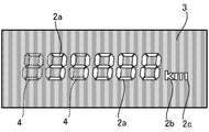
- FIG. 1 It is a figure for demonstrating schematic structure of the liquid crystal display element which concerns on one Embodiment of this invention. It is a figure which shows an example of a display element.
- A is a figure for demonstrating the relationship between the orientation direction of a liquid crystal layer, and the orientation direction of a liquid crystalline polymer layer.
- B is a figure for demonstrating the relationship between F absorption axis and R absorption axis. It is a figure for demonstrating the contrast characteristic etc. of the liquid crystal display element which concerns on one Embodiment of this invention, and the liquid crystal display element which concerns on a prior art example and a comparative example. It is a figure of the graph which shows the relationship between F absorption axis angle and contrast in a plurality of viewing angles.
- (A) is a figure which shows the table
- (B) is a table showing the contrast when the R absorption axis angle and the viewing angle are changed within a predetermined range. It is a figure for demonstrating a viewing angle and an azimuth.
- a liquid crystal display element 100 according to the present embodiment shown in FIG. 1 is configured as a super twisted nematic (STN) type, and includes a liquid crystal element 10, a first polarizing plate 20, a second polarizing plate 30, and a twisted phase difference.
- a plate 40 is configured as a super twisted nematic (STN) type, and includes a liquid crystal element 10, a first polarizing plate 20, a second polarizing plate 30, and a twisted phase difference.
- STN super twisted nematic
- the liquid crystal element 10 includes a first substrate 11 and a second substrate 12, which are a pair of transparent substrates facing each other, and a liquid crystal layer 13.
- the first substrate 11 and the second substrate 12 are made of, for example, glass, plastic, or the like, and are arranged so as to face each other with the liquid crystal layer 13 interposed therebetween, and their main surfaces (opposing surfaces) are parallel to each other.
- the first substrate 11 is located closer to the observer 1 who visually recognizes the display element than the liquid crystal layer 13.
- a transparent electrode 11a and an alignment film 11b are provided on the liquid crystal layer 13 side of the first substrate 11.
- the alignment film 11b is located closer to the liquid crystal layer 13 than the transparent electrode 11a.
- a transparent electrode 12a and an alignment film 12b are provided on the liquid crystal layer 13 side of the second substrate 12.
- the alignment film 12b is located closer to the liquid crystal layer 13 than the transparent electrode 12a. If necessary, an insulating film may be provided between the transparent electrode 11a and the alignment film 11b and between the transparent electrode 12a and the alignment film 12b.
- the transparent electrodes 11a and 12a are made of, for example, an ITO (Indium Tin Oxide) film mainly composed of indium oxide, and each is patterned into a predetermined shape.
- the transparent electrode 11a is formed on the surface of the first substrate 11 on the liquid crystal layer 13 side, and the transparent electrode 12a is formed on the surface of the second substrate 12 on the liquid crystal layer 13 side by a known method (sputtering, vapor deposition, etching, etc.). ing.
- the transparent electrodes 11a and 12a may be formed of a material containing a ⁇ -conjugated conductive polymer such as polythiophene.
- the transparent electrode 11a is configured as a common electrode, and the transparent electrode 12a is configured as a segment electrode. A voltage is applied to both electrodes by a passive drive system. That is, the liquid crystal display element 100 is a segment display type and configured as a passive drive type liquid crystal display element.
- the transparent electrode 11a may be configured as a segment electrode, and the transparent electrode 12a may be configured as a common electrode.
- the liquid crystal display element 100 has the predetermined shape in a region where the transparent electrodes 11a and 12a overlap in the normal direction of the opposing surfaces of the first substrate 11 and the second substrate 12 (hereinafter also simply referred to as the substrate normal direction).
- the display element corresponding to is displayed.
- the display element is an element for indicating information displayed on the liquid crystal display element 100, and refers to a symbol (including letters and numbers), a figure, or a combination thereof.
- the liquid crystal display element 100 displays the display element substantially white on the substantially black background region by transmitting light in the region where the ON voltage is applied to the transparent electrodes 11a and 12a (the display element is set to the display state). ) It is configured as a so-called negative display type (normally black mode).
- the liquid crystal display element 100 is an example configured as a 7-segment display, and the liquid crystal display element 100 shows information on the total travel distance of a certain vehicle by indicating numerical values and units.
- a combination of seven segments 2a shown the numeral “8” when all of them are displayed
- a segment 2b displaying the alphabet “k” in the display state
- “m” in the display state.
- the liquid crystal display element 100 displays information that the total travel distance of the current vehicle is “34888 km” in combination with the segment 2c that displays the alphabet.
- Segments 2a to 2c are examples of display elements.
- a region where the transparent electrode 11a and the transparent electrode 12a do not overlap and a region where no ON voltage is applied become the substantially black background region 3.
- the routing electrode formed in the background region 3 is omitted.
- the alignment films 11b and 12b are in contact with the liquid crystal layer 13 and are for defining the alignment state of liquid crystal molecules included in the liquid crystal layer 13, and are made of, for example, polyimide and formed by a known method (for example, flexographic printing). Is done.
- the alignment film 11b is formed so as to cover the transparent electrode 11a from the liquid crystal layer 13 side
- the alignment film 12b is formed so as to cover the transparent electrode 12a from the liquid crystal layer 13 side.
- the alignment films 11b and 12b are rubbed. Thereby, the alignment direction of the liquid crystal molecules included in the liquid crystal layer 13 is defined.
- the alignment treatment performed on the alignment films 11b and 12b is not limited to the rubbing treatment, and may be other known treatments such as a photo-alignment treatment and a protrusion alignment treatment. By these treatments, the major axis direction of the liquid crystal molecules May be regulated. The rubbing direction applied to the alignment films 11b and 12b will be described later.
- a liquid crystal material is sealed in a sealed space formed by a sealing material (not shown) for joining the first substrate 11 and the second substrate 12 and both substrates.
- the value of retardation ⁇ nd1 which is the product of the refractive index anisotropy ⁇ n1 of the liquid crystal layer 13 and the cell gap d1, is set substantially equal to the value of retardation ⁇ nd2 of the twisted phase difference plate 40 described later. What value is set will be described together with the explanation of the twisted phase difference plate 40.
- the alignment direction of the liquid crystal molecules in the liquid crystal layer 13 is regulated by the alignment film 11b and the alignment film 12b as shown in FIG. Specifically, as shown in the figure, with reference to an axis along the left-right direction (same as the left-right direction in FIG. 3A) when the viewer 1 views the liquid crystal display element 100 from the substrate normal direction. In addition, when the angle is defined so that the angle increases counterclockwise from 0 ° (that is, the 3:00 direction is 0 ° as viewed from the observer 1), the liquid crystal at a position close to the first substrate 11 is used.
- the alignment direction 13a of molecules (hereinafter referred to as F liquid crystal molecule alignment direction 13a) is set to 0 °, and the alignment direction 13b of liquid crystal molecules at a position close to the second substrate 12 (hereinafter referred to as R liquid crystal molecule alignment direction 13b). Is also set in the 0 ° direction. If the viewer 1 side is the front side (upper side in FIG. 1) and the opposite side is the back side (lower side in FIG. 1) in the liquid crystal display element 100, the rubbing direction of the alignment film 11b on the front side is F liquid crystal. The rubbing direction of the alignment film 12b on the back side coincides with the R liquid crystal molecular alignment direction 13b (parallel rubbing).
- the liquid crystal molecules of the liquid crystal layer 13 have a major axis orientation of about 180 ° between the end of the liquid crystal layer 13 on the first substrate 11 side and the end of the second substrate 12 side. And is oriented so as to rotate (turn) little by little from one substrate side to the other substrate side (chiral structure).
- the liquid crystal layer 13 when no voltage is applied has chirality.
- the F liquid crystal molecule alignment direction 13a is twisted approximately 180 ° counterclockwise with respect to the R liquid crystal molecule alignment direction 13b.
- approximately 180 ° is a concept including exactly 180 ° and also includes a case where the angle is shifted from 180 ° due to an assembly error or the like.
- substantially is used in the same meaning.
- the liquid crystal molecules at positions close to the first substrate 11 and the second substrate 12 are arranged with an inclination with respect to the substrate surface (pretilt is given).
- This tilt angle is called a pretilt angle ⁇ p.
- the pretilt angle ⁇ p is 0.2 ° or more and 1.0 ° or less (0.2 °) in order to improve the steepness of the liquid crystal display element 100 in a favorable manner.
- the pretilt angle is set to about 3 ° to 4 °.
- the angle ⁇ p is set smaller than the conventional one.
- the first polarizing plate 20 and the second polarizing plate 30 emit light incident from the front side or the back side as linearly polarized light along a transmission axis perpendicular to the absorption axis.
- Both polarizing plates are, for example, iodine-based polarizing plates (polarizing filters).
- the first polarizing plate 20 and the second polarizing plate 30 face each other, the first polarizing plate 20 is located on the side opposite to the liquid crystal layer 13 side of the first substrate 11, and the second polarizing plate 30
- the two substrates 12 are located on the side opposite to the liquid crystal layer 13 side. In other words, the first polarizing plate 20 is located closer to the viewer 1 viewing the display element than the liquid crystal layer 13.
- FIG. 3B is a diagram corresponding to FIG.
- the first polarizing plate 20 and the second polarizing plate 30 are set so as to satisfy the following conditions (1) to (3).
- the angle ⁇ 1 (see FIG. 3B), which is an angle between the liquid crystal alignment axis D and the first absorption axis 21 and is an acute angle, is 45 ° or more.
- the angle ⁇ 2 (see FIG. 3B) that is an acute angle with the absorption axis 31 is 45 ° or more.
- the angle between the F absorption axis 21 and the R absorption axis 31 is an acute angle.
- the angle ⁇ (see FIG. 3B) is 85 ° or more and less than 90 °.
- the angle ⁇ is 88 °. How the conditions (1) to (3) (hereinafter referred to as “liquid crystal alignment axis-absorption axis condition”) are determined will be described later.
- the twisted phase difference plate (twisted phase difference film) 40 is located between the liquid crystal element 10 and the second polarizing plate 30, and includes both the first transparent portion 41 and the second transparent portion 42. And a liquid crystalline polymer layer 43 positioned between the two.
- the first transparent portion 41 is located closer to the liquid crystal element 10 than the second transparent portion 42.
- the twisted phase difference plate 40 is subjected to an alignment treatment so that the twist angle of the polymer molecules of the liquid crystalline polymer layer 43 is approximately 180 °. This alignment treatment is appropriately performed by a known method. Specifically, as shown in FIG.
- the alignment direction 43a of the polymer molecules at the position close to the first transparent portion 41 in the liquid crystalline polymer layer 43 (hereinafter referred to as F molecule alignment direction 43a) is In the 90 ° direction, the polymer molecule orientation direction 43b (hereinafter referred to as the R molecule orientation direction 43b) at a position close to the second transparent portion 42 is set to the 90 ° direction. That is, when viewed from the normal direction of the substrate, the R liquid crystal molecule alignment direction 13b and the F molecule alignment direction 43a are substantially orthogonal to each other.
- the F molecule alignment direction 43a is twisted by approximately 180 ° clockwise with respect to the R molecule alignment direction 43b. That is, the twist direction of the polymer molecules is opposite to the twist direction of the liquid crystal molecules.
- the first transparent portion 41 is made of, for example, a transparent film-like substrate, and the liquid crystalline polymer layer 43 is formed by the liquid crystalline polymer applied on one surface of the substrate.
- the twisted phase difference plate 40 is formed in this way as an example.
- the value of retardation ⁇ nd1 of the liquid crystal layer 13 and the value of retardation ⁇ nd2 of the liquid crystalline polymer layer 43 are set to be approximately equal.
- the front contrast (contrast in the substrate normal direction) of the liquid crystal display element 100 is improved.
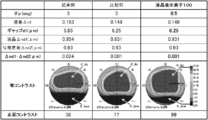
- the refractive index anisotropy (birefringence index) ⁇ n of the liquid crystal layer 13 is set to 0.149, and the cell gap d1 is set to 6.25 ⁇ m.
- the value of the retardation ⁇ nd1 which is the product of the refractive index anisotropy ⁇ n1 of the liquid crystal layer 13 and the cell gap (thickness of the liquid crystal layer 13) d1 is about 0.931 ⁇ m (see FIG. 4).
- the value of retardation ⁇ nd2, which is the product of the refractive index anisotropy ⁇ nd2 of the liquid crystalline polymer layer 43 and the thickness of the liquid crystalline polymer layer 43 is set to about 0.93 ⁇ m (see FIG. 4).
- the value obtained by subtracting ⁇ nd2 from ⁇ nd1 is 0.001, and it can be seen that both are set to be approximately equal.
- the twisted phase difference plate 40 is, for example, a temperature-compensated twisted phase difference plate that can suppress a change in color even with respect to a temperature change, and the value of ⁇ nd2 becomes smaller at a high temperature. ing.
- the value of retardation ⁇ nd1 of the liquid crystal layer 13 and the value of retardation ⁇ nd2 of the liquid crystalline polymer layer 43 are substantially equal.
- the pretilt angle ⁇ p is set to be smaller than that of the conventional STN and the cell gap d1 is set to a value of 6.0 ⁇ m or more, thereby making the liquid crystal display element 100 more steep. Is improved well.
- the cell gap d1 is set to 6.25 ⁇ m (see FIG. 4). Note that the cell gap d1 is maintained by a spacer (not shown) provided between the first substrate 11 and the second substrate 12.
- the liquid crystal display element 100 On the back side of the second polarizing plate 30, for example, a reflective layer (not shown) is provided.
- the reflection layer is made of a mirror or a half mirror, and the liquid crystal display element 100 is configured as a so-called reflection type or semi-transmission type.
- the liquid crystal display element 100 may be configured as a transmissive type that does not include a reflective layer and performs transmissive display using light from a backlight.
- the liquid crystal display element 100 of the present embodiment transmits light in a region where the liquid crystal molecules of the liquid crystal layer 13 are in an initial alignment state (a state having chirality) by applying no voltage or applying an OFF voltage.
- it is configured as a so-called negative display type (normally black mode) that transmits light in a region where liquid crystal molecules rise due to application of an ON voltage.
- the liquid crystal display element 100 having the above configuration is mounted on a vehicle, for example, so that the contrast is good at the viewing angle from above (that is, the display from above is easy to see). ),
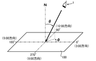
- the viewing angle is an inclination angle ⁇ of the line of sight by the observer 1 with respect to the substrate normal N as shown in FIG.
- the azimuth angle ⁇ shown in the figure is a counterclockwise angle of the orthogonal projection of the line of sight onto the substrate with respect to the axis along the left-right direction as viewed from the observer 1. That is, the liquid crystal display element 100 is set so that the contrast is good when the viewing angle from above, that is, the azimuth angle ⁇ is near 90 ° and the viewing angle ⁇ is greater than 0 °.
- the contrast is a value obtained by dividing the transmittance at the time of applying the ON voltage by the transmittance at the time of applying the OFF voltage, and the larger the value, the easier the display is to be seen.
- voltages that give the maximum contrast at 1/48 Duty and 1/4 Bias are applied, respectively.
- the ON voltage 2.18 V and the OFF voltage 1.96 V in the conventional example the ON voltage 2.42 V and the OFF voltage 2.18 V in the comparative example, and the ON voltage 2.60 V and OFF in the liquid crystal display element 100.
- the voltage is set to 2.34V.
- the pretilt angle ⁇ p is 0.5 °
- the cell gap d1 is 6.25 ⁇ m
- the retardation ⁇ nd1 of the liquid crystal layer 13 is 0.931
- the retardation ⁇ nd2 of the twisted phase difference plate 40 is 0.93.
- ⁇ nd1 ⁇ nd2 0.001. That is, ⁇ nd1 ⁇ nd2).
- ⁇ p 3 ° is set larger
- the retardation ⁇ nd2 of the twisted phase difference plate 40 is a liquid crystal display.
- the iso-contrast characteristics and front contrast characteristics for “Example” are also shown.
- the liquid crystal display element 100 is configured so as to satisfy the above-mentioned “liquid crystal alignment axis-absorption axis condition”.
- the numerical values (0, 45, 90, etc.) shown along the outer periphery of the circle represent the azimuth angle ⁇ and correspond to the broken line extending concentrically.
- the indicated numerical values (10, 20, 30, etc.) represent the viewing angle ⁇ .
- the comparative example in which the value of the cell gap d1 is larger than the conventional example is the upper viewing angle direction (the direction in which ⁇ is in the vicinity of 90 ° and the viewing angle ⁇ is greater than 0 °). It can be seen that the high contrast region C_hi having a contrast of 20.7 or more spreads well.
- the liquid crystal display element 100 in which the pretilt angle ⁇ p is set smaller than the comparative example shows that the high contrast region C_hi spreads more favorably in the upper viewing angle direction. Recognize.
- the comparative example has a smaller area occupied by the low contrast region C_low than the conventional example, and the liquid crystal display element 100 has a lower contrast region than the comparative example. It can be seen that the range occupied by C_low is small. That is, in the liquid crystal display element 100, since the pretilt angle ⁇ p is set small (for example, 0.5 °), the steepness is improved, the contrast is improved, and the cell gap d1 is set large (example). 625 ⁇ m), it can be seen that the contrast is improved.
- the value of the retardation ⁇ nd1 of the liquid crystal layer 13 is set to be substantially equal to the value of the retardation ⁇ nd2 of the twisted phase difference plate 40. It can be seen that “99” is higher than “38” in the conventional example and “77” in the comparative example, and is excellent in display quality.
- FIG. 5 and FIG. 6 show how much the contrast in a specific viewing angle direction can be maintained, that is, how the above-mentioned “liquid crystal alignment axis-absorption axis condition” is determined, no matter how much the axis direction is shifted. This will be described with reference to (a) and (b).
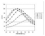
- FIG. 5 is a graph showing the relationship between the angle of the F absorption axis 21 and the contrast when the viewing angle ⁇ is changed by 10 ° in the range of 0 ° to 40 °. This graph is created based on the data shown in FIG.
- the contrast shown in FIG. 6A is derived by simulation using a simulation software “LCD MASTER ver. 8.1” manufactured by Shintech Co., Ltd. The same applies to the equicontrast characteristics and the front contrast in FIG. 4 and the contrast shown in FIG. 6B.
- the cell gap d1 of the liquid crystal layer 13 was set to 6.25 ⁇ m.
- the F liquid crystal molecular alignment direction 13a, the R liquid crystal molecular alignment direction 13b, the F molecular alignment direction 43a, and the R molecular alignment direction 43b satisfy the above-described relationship shown in FIG.
- FIG. 6A shows a state in which the angle direction of the F absorption shaft 21 is changed in the range of 40 ° to 55 ° while the R absorption shaft 31 is kept in the 135 ° direction.
- the azimuth angle ⁇ is 90 °.
- the viewing angle ⁇ at which the contrast is maximized increases as the angle of the F absorption axis 21 is increased from 45 °. That is, it can be seen that if the angle is increased in this way, the display quality can be improved when the observer 1 looks into the liquid crystal display element 100 from above.
- the F absorption axis 21 is 52 °
- the contrast is as low as 50
- the viewing angle ⁇ at this time is 40 °. It cannot be adopted as a product.
- the present inventors have found that the angle direction of the F absorption axis 21 is optimally in the range of 45 ° to 50 ° when the R absorption axis 31 is maintained in the 135 ° direction. It was.
- the angle direction of the R absorption axis 31 is optimally in the range of 135 ° to 130 ° when the F absorption axis 21 is kept in the 45 ° direction. It was.
- the relative angular relationship between the F absorption axis 21 and the R absorption axis 31 is “the angle formed by the F absorption axis 21 and the R absorption axis 31”. If the angle of the acute angle ⁇ (see FIG. 3B) is 85 ° or more and less than 90 °, it can be seen that good contrast can be obtained in the range of the viewing angle ⁇ of 0 ° to 30 °. (Especially, 10 ° ⁇ ⁇ ⁇ 20 ° is the best viewing direction since the contrast becomes the maximum value when ⁇ is in the range of 10 ° to 20 °).
- the angle ⁇ 1 that is the angle between the liquid crystal alignment axis D and the F absorption axis 21 and is an acute angle is 45 ° or more
- the liquid crystal alignment axis It can be seen that the condition that the angle ⁇ 2 formed by D and the R absorption axis 31 and an acute angle ⁇ 2 is 45 ° or more must also be satisfied. In this way, the above-mentioned “liquid crystal alignment axis-absorption axis condition” was derived.
- the liquid crystal display element 100 described above includes a first substrate 11 and a second substrate 12 facing each other, a liquid crystal layer 13 positioned between the first substrate 11 and the second substrate 12, a first substrate 11 and a second substrate.
- a liquid crystal element 10 having transparent electrodes 11a and 12a that are provided on the surface of each substrate 12 on the liquid crystal layer 13 side and patterned in a predetermined shape, and on the opposite side of the first substrate 11 from the liquid crystal layer 13 side.
- the first polarizing plate 20 positioned, the second polarizing plate 30 facing the first polarizing plate 20 located on the side opposite to the liquid crystal layer 13 side of the second substrate 12, the liquid crystal element 10 and the second polarizing plate 30.
- a twisted phase difference plate 40 having a liquid crystalline polymer layer 43, and a display element corresponding to the predetermined shape by applying a voltage to the liquid crystal layer 13 from the transparent electrodes 11a and 12a.
- Super twisted nematic liquid crystal display In the element 100, the liquid crystal molecules of the liquid crystal layer 13 are aligned with a twist angle of approximately 180 °, and the polymer molecules of the liquid crystalline polymer layer 43 are aligned with a twist angle of approximately 180 °.
- the twist direction of the liquid crystal layer 13 is opposite to the twist direction of the polymer molecules, the pretilt angle ⁇ p of the liquid crystal layer 13 is 0.2 ° or more and 1.0 ° or less, and the thickness of the liquid crystal layer 13 (cell gap d1).
- the alignment direction of the liquid crystal molecules (R liquid crystal molecule alignment direction 13b) on the phase difference plate 40 side and the alignment direction of polymer molecules on the liquid crystal element 10 side (F molecular alignment direction 43a) among the liquid crystalline polymer molecules are substantially orthogonal to each other, and the liquid crystal
- the angle ⁇ 1 formed between the direction axis D and the F absorption axis 21 and an acute angle is 45 ° or more
- the angle formed between the liquid crystal alignment axis D and the R absorption axis 31 is an acute angle.
- the angle ⁇ 2 is 45 ° or more
- the angle ⁇ which is an angle formed by the F absorption axis 21 and the R absorption axis 31 and is an acute angle, is 85 ° or more and less than 90 °.
- the pretilt angle ⁇ p is preferably 0.2 ° or more and 0.6 ° or less.
- the twisted phase difference plate 40 may be disposed between the liquid crystal element 10 and the first polarizing plate 20. Good. The same effect can be obtained also by this.
- the liquid crystal display element 100 is not limited to the segment display type, and may be a passive matrix type. In this case, a pixel (dot) is an example of a display element. Further, the liquid crystal display element 100 is not limited to a vehicle-mounted one, and can be applied to all devices that require high contrast in a specific viewing angle direction.
- the present invention can be used for a liquid crystal display element, particularly a super twisted nematic type liquid crystal display element provided with a twisted phase difference plate having a liquid crystalline polymer layer.
- liquid crystal display element 10 liquid crystal element 11 first substrate 11a transparent electrode 11b alignment film 12 second substrate 12a transparent electrode 12b alignment film 13 liquid crystal layer 13a F liquid crystal molecule alignment direction 13b R liquid crystal molecule alignment direction 20 first polarizing plate 21 F absorption Axis 30 second polarizing plate 31 R absorption axis 40 twisted phase difference plate 43 liquid crystal polymer layer 43a F molecule alignment direction 43b R molecule alignment direction D liquid crystal alignment axis
Landscapes
- Physics & Mathematics (AREA)
- Liquid Crystal (AREA)
- Nonlinear Science (AREA)
- Spectroscopy & Molecular Physics (AREA)
- Mathematical Physics (AREA)
- Chemical & Material Sciences (AREA)
- Crystallography & Structural Chemistry (AREA)
- General Physics & Mathematics (AREA)
- Optics & Photonics (AREA)
Abstract
特定の視角方向におけるコントラストと急峻性を良好にする。 STN型の液晶表示素子は、液晶性ポリマー層を有するねじれ位相差板を備える。液晶素子の液晶層の液晶分子は、略180°のねじれ角で配向し、液晶性ポリマー層のポリマー分子は、略180°のねじれ角で配向し、互いのねじれ方向は逆方向である。プレチルト角は、0.2°以上1.0°以下であり、液晶層の厚みは、6.0μm以上であり、液晶層のリタデーションと液晶性ポリマー層のリタデーションとは、略等しい。R液晶分子配向方向13bとF分子配向方向43aとは略直交し、液晶配向軸DとF吸収軸21とのなす角α1の角度は、45°以上であり、液晶配向軸DとR吸収軸31とのなす角α2の角度は、45°以上であり、F吸収軸21とR吸収軸31とのなす角βの角度は、85°以上90°未満である。
Description
本発明は、液晶表示素子に関し、詳しくは、液晶性ポリマー層を有するねじれ位相差板を備えた超ねじれネマティック型の液晶表示素子に関する。
超ねじれネマティック(STN(Super Twisted Nematic))型の液晶表示素子では、何の対策も講じないとSTN型特有の背景着色が顕著に発生し、表示品位が低下するため、背景着色を解消するための位相差板が設けられるのが一般的である。特に、高耐久性が要求される場合には、周囲温度による見栄えの変化を無くすために、位相差板として液晶の温度特性を踏まえた液晶性ねじれ位相差板(液晶性ポリマー層を有するねじれ位相差板)が採用される。
例えば、液晶性ねじれ位相差板を備えるSTN型液晶表示素子として、特許文献1に開示されたものがある。特許文献1に係るSTN型液晶表示素子は、ツイスト角が180°~270°の範囲に設定され、液晶層のリタデーションΔnd1が0.7~0.9μmで、且つ、このΔnd1から液晶性ねじれ位相差板のリタデーションΔnd2を減じた値が0.1~0.3μmに設定されたものである。
ところで、STN型液晶表示素子が特定用途に専用のものであると、特定の視角方向において高いコントラストが求められる場合がある。一例として、STN型液晶表示素子が車載用である場合は、座席に座る運転者等の視認者からの見栄えが良いことが求められるため、上方向からの視角において高いコントラストが要求される。しかし、特許文献1に係るSTN型液晶表示素子は、正面コントラストを重視した構成となっていた。
また、STN型液晶表示素子は、液晶分子のツイスト角180°~240°程度と大きいため、プレチルト角(基板-液晶界面における液晶分子の傾きの角度)が3度ないしは4度程度と、大きめに設定されていることが一般的であるため、良好な急峻性を得る点で改善の余地があった。
本発明は、上記実状に鑑みてなされたものであり、特定の視角方向におけるコントラストと急峻性とが良好な液晶表示素子を提供することを目的とする。
上記目的を達成するため、本発明に係る液晶表示素子は、
互いに対向する第1基板及び第2基板と、前記第1基板と前記第2基板の間に位置する液晶層と、前記第1基板と前記第2基板の各々の前記液晶層側の面に設けられ、所定の形状にパターニングされた透明電極と、を有する液晶素子と、
前記第1基板の前記液晶層側とは反対側に位置する第1偏光板と、
前記第2基板の前記液晶層側とは反対側に位置して前記第1偏光板と対向する第2偏光板と、
前記液晶素子と前記第1偏光板との間、又は、前記液晶素子と前記第2偏光板との間に位置し、液晶性ポリマー層を有するねじれ位相差板と、を備え、
前記透明電極から前記液晶層に電圧が印加されることで前記所定の形状に対応した表示要素を表示する超ねじれネマティック型の液晶表示素子であって、
前記液晶層の液晶分子は、略180°のねじれ角で配向しており、
前記液晶性ポリマー層のポリマー分子は、略180°のねじれ角で配向しており、
前記液晶分子のねじれ方向は、前記ポリマー分子のねじれ方向と逆方向であり、
前記液晶層のプレチルト角の角度は、0.2°以上1.0°以下であり、
前記液晶層の厚みは、6.0μm以上であり、
前記液晶層のリタデーションの値と前記液晶性ポリマー層のリタデーションの値とは、略等しく、
前記第1基板及び前記第2基板の対向面の法線方向から見て、前記液晶層のうち前記ねじれ位相差板側の液晶分子の配向方向と、前記液晶性ポリマー分子のうち前記液晶素子側のポリマー分子の配向方向とは略直交し、
前記液晶層のうち前記ねじれ位相差板側の液晶分子の配向方向に沿う軸を液晶配向軸とし、前記第1偏光板の吸収軸を第1吸収軸とし、前記第2偏光板の吸収軸を第2吸収軸とすると、
前記液晶配向軸と前記第1吸収軸とのなす角であって鋭角となる角の角度は、45°以上であり、
前記液晶配向軸と前記第2吸収軸とのなす角であって鋭角となる角の角度は、45°以上であり、
前記第1吸収軸と前記第2吸収軸とのなす角であって鋭角となる角の角度は、85°以上90°未満である、
ことを特徴とする。
互いに対向する第1基板及び第2基板と、前記第1基板と前記第2基板の間に位置する液晶層と、前記第1基板と前記第2基板の各々の前記液晶層側の面に設けられ、所定の形状にパターニングされた透明電極と、を有する液晶素子と、
前記第1基板の前記液晶層側とは反対側に位置する第1偏光板と、
前記第2基板の前記液晶層側とは反対側に位置して前記第1偏光板と対向する第2偏光板と、
前記液晶素子と前記第1偏光板との間、又は、前記液晶素子と前記第2偏光板との間に位置し、液晶性ポリマー層を有するねじれ位相差板と、を備え、
前記透明電極から前記液晶層に電圧が印加されることで前記所定の形状に対応した表示要素を表示する超ねじれネマティック型の液晶表示素子であって、
前記液晶層の液晶分子は、略180°のねじれ角で配向しており、
前記液晶性ポリマー層のポリマー分子は、略180°のねじれ角で配向しており、
前記液晶分子のねじれ方向は、前記ポリマー分子のねじれ方向と逆方向であり、
前記液晶層のプレチルト角の角度は、0.2°以上1.0°以下であり、
前記液晶層の厚みは、6.0μm以上であり、
前記液晶層のリタデーションの値と前記液晶性ポリマー層のリタデーションの値とは、略等しく、
前記第1基板及び前記第2基板の対向面の法線方向から見て、前記液晶層のうち前記ねじれ位相差板側の液晶分子の配向方向と、前記液晶性ポリマー分子のうち前記液晶素子側のポリマー分子の配向方向とは略直交し、
前記液晶層のうち前記ねじれ位相差板側の液晶分子の配向方向に沿う軸を液晶配向軸とし、前記第1偏光板の吸収軸を第1吸収軸とし、前記第2偏光板の吸収軸を第2吸収軸とすると、
前記液晶配向軸と前記第1吸収軸とのなす角であって鋭角となる角の角度は、45°以上であり、
前記液晶配向軸と前記第2吸収軸とのなす角であって鋭角となる角の角度は、45°以上であり、
前記第1吸収軸と前記第2吸収軸とのなす角であって鋭角となる角の角度は、85°以上90°未満である、
ことを特徴とする。
本発明によれば、特定の視角方向におけるコントラストと急峻性とが良好な液晶表示素子を提供することができる。
本発明の一実施形態について図面を参照して説明する。
図1に示す本実施形態に係る液晶表示素子100は、超ねじれネマティック(STN)型のものとして構成され、液晶素子10と、第1偏光板20と、第2偏光板30と、ねじれ位相差板40と、を備える。
液晶素子10は、図1に示すように、互いに対向する一対の透明基板である第1基板11及び第2基板12と、液晶層13と、を備える。第1基板11と第2基板12とは、例えば、ガラス、プラスチック等から構成され、液晶層13を挟んで対向するように、且つ、互いの主面(対向面)が平行となるように配置されている。第1基板11は、液晶層13よりも、表示要素を視認する観察者1側に位置する。
第1基板11の液晶層13側には、透明電極11aと配向膜11bとが設けられている。配向膜11bは、透明電極11aよりも液晶層13側に位置する。第2基板12の液晶層13側には、透明電極12aと配向膜12bとが設けられている。配向膜12bは、透明電極12aよりも液晶層13側に位置する。なお、必要に応じて、透明電極11aと配向膜11bとの間、透明電極12aと配向膜12bとの間に、絶縁膜を設けてもよい。
透明電極11a,12aは、例えば酸化インジウムを主成分とするITO(Indium Tin Oxide)膜から構成され、各々が所定の形状にパターニングされている。透明電極11aは第1基板11の液晶層13側の面上に、透明電極12aは第2基板12の液晶層13側の面上に、公知の方法(スパッタ、蒸着、エッチング等)により形成されている。なお、透明電極11a,12aは、ポリチオフェン等のπ共役系導電性高分子を含む材料により形成されていてもよい。
透明電極11aはコモン電極として、透明電極12aはセグメント電極として構成されている。両電極には、パッシブ駆動方式で電圧が印加される。つまり、液晶表示素子100は、セグメント表示型であってパッシブ駆動方式の液晶表示素子として構成されている。なお、透明電極11aがセグメント電極、透明電極12aがコモン電極として構成されてもよい。
液晶表示素子100は、第1基板11及び第2基板12の対向面の法線方向(以下、単に、基板法線方向ともいう)において透明電極11aと12aとが重なる領域において、前記所定の形状に対応した表示要素を表示する。ここで、表示要素とは、液晶表示素子100が表示する情報を示すための要素であり、記号(文字、数字を含む)、図形、又はこれらの組み合わせをいう。なお、液晶表示素子100は、透明電極11a,12aにON電圧が印加された領域で光を透過させることによって、略黒の背景領域に表示要素を略白く表示する(表示要素を表示状態とする)所謂ネガ表示型(ノーマリブラックモード)のものとして構成されている。
液晶表示素子100が表示する情報の一例を図2に示す。同図では、液晶表示素子100が7セグメントディスプレイとして構成された例で、液晶表示素子100が数値と単位とを示すことにより、ある車両の総走行距離の情報を示している例である。同図では、7つのセグメント2a(これらがすべて表示された状態で数字の「8」を示す)の組合せと、表示状態で「k」というアルファベットを表示するセグメント2bと、表示状態で「m」というアルファベットを表示するセグメント2cと、の組合せで、液晶表示素子100が現在の車両の総走行距離が「34888km」であるという情報を表示している。セグメント2a~2cは、表示要素の一例である。液晶表示素子100では、透明電極11aと透明電極12aとが重ならない領域、及び、ON電圧が印加されていない領域が略黒の背景領域3となる。なお、図2では、背景領域3において形成されている引き回し電極を省略して表している。
配向膜11b,12bは、各々、液晶層13と接し、液晶層13が含む液晶分子の配向状態を規定するためのものであり、例えばポリイミドからなり、公知の方法(例えば、フレクソ印刷)によって形成される。配向膜11bは透明電極11aを液晶層13側から覆うように形成されており、配向膜12bは透明電極12aを液晶層13側から覆うように形成されている。
配向膜11b、12bには、ラビング処理が施されている。これにより、液晶層13が含む液晶分子の配向方向が規定される。なお、配向膜11b,12bに施される配向処理は、ラビング処理に限らず、光配向処理、突起配向処理等の他の公知の処理によってもよく、これらの処理によって、液晶分子の長軸方向が規制されていてもよい。配向膜11b、12bに施されたラビング方向については後述する。
図1に戻って、液晶層13は、第1基板11及び第2基板12を接合するためのシール材(図示せず)と両基板とによって形成される密閉空間に液晶材が封入されることによって形成される。液晶層13の屈折率異方性Δn1とセルギャップd1との積であるリタデーションΔnd1の値は、後述するねじれ位相差板40のリタデーションΔnd2の値と略等しく設定されている。どのような値で設定されているかは、ねじれ位相差板40についての説明で併せて説明する。
液晶層13の液晶分子の配向方向は、配向膜11b及び配向膜12bにより、図3(a)に示すように規制されている。具体的には、観察者1が基板法線方向から液晶表示素子100を見た場合の左右方向(図3(a)における左右方向と同じ)に沿った軸線を基準として、同図に示すように、反時計回りに角度が0°から増加するように、角度を定義した場合(つまり、観察者1から見て3:00方向が0°方向)、第1基板11に近接した位置の液晶分子の配向方向13a(以下、F液晶分子配向方向13aという)は0°方向に設定され、第2基板12に近接した位置の液晶分子の配向方向13b(以下、R液晶分子配向方向13bという)も0°方向に設定されている。なお、液晶表示素子100において観察者1側を前面側(図1において上側)、その反対側を背面側(図1において下側)とすれば、前面側の配向膜11bのラビング方向がF液晶分子配向方向13aと一致し、背面側の配向膜12bのラビング方向がR液晶分子配向方向13bと一致する(パラレルラビング)。これにより、液晶層13の液晶分子は、その長軸の向きが液晶層13の第1基板11側の端部と第2基板12側の端部とでツイスト角(ねじれ角)が略180°の角度でねじれるとともに、一方の基板側から他方の基板側にいくにつれて少しずつ回転(旋回)するように配向する(カイラル構造)。このようにして、電圧無印加時における液晶層13は、カイラリティを有する。
本実施形態では、F液晶分子配向方向13aは、R液晶分子配向方向13bに対して、反時計回りに略180°ねじれている。なお、略180°とは、丁度180°も含み、且つ、180°から組み付け誤差等により角度がずれた場合も含む概念である。以下の記載においても、「略」は同様の意味で用いる。
また、液晶層13では、第1基板11及び第2基板12各々に近接する位置の液晶分子は、基板面に対して傾きをもって配列している(プレチルトが付与されている)。この傾き角は、プレチルト角θpと呼ばれ、本実施形態では、液晶表示素子100の急峻性を良好に高めるため、プレチルト角θpは、0.2°以上1.0°以下(0.2°≦θp≦1.0°)、好ましくは、0.2°以上0.6°以下(0.2°≦θp≦0.6°)の範囲で設定されている。従来のSTN型液晶表示素子では、前述のようにプレチルト角は、3°~4°程度に設定されていたが、本実施形態に係る液晶表示素子100では、急峻性を良好に高めるため、プレチルト角θpを、このように従来のものよりも小さく設定している。
第1偏光板20、第2偏光板30は、その前面側又は背面側から入射する光を吸収軸に直交する透過軸に沿った直線偏光として出射するものである。両偏光板は、例えば、ヨウ素系の偏光板(偏光フィルタ)からなる。第1偏光板20と第2偏光板30とは、互いに対向し、第1偏光板20は、第1基板11の液晶層13側とは反対側に位置し、第2偏光板30は、第2基板12の液晶層13側とは反対側に位置する。つまり、第1偏光板20は、液晶層13よりも、表示要素を視認する観察者1側に位置する。
液晶表示素子100を基板法線方向から見ると、第1偏光板20の吸収軸21(以下、F吸収軸21という)と第2偏光板30の吸収軸31(以下、R吸収軸31)との関係は、図3(b)に示すようになる。なお、図3(b)における角度の基準は、図3(a)と同様である。つまり、図3(b)は、図3(a)と対応した図となっている。
ここで、R液晶分子配向方向13bに沿う軸を液晶配向軸Dとすると(なお、液晶層13のツイスト角は180°であるため、F液晶分子配向方向13aに沿う軸とも言える。)、第1偏光板20と第2偏光板30とは、具体的には、以下の(1)~(3)の条件を満たすように設定されている。
(1)液晶配向軸Dと第1吸収軸21とのなす角であって鋭角となる角α1(図3(b)参照)の角度は、45°以上
(2)液晶配向軸Dと第2吸収軸31とのなす角であって鋭角となる角α2(図3(b)参照)の角度は、45°以上
(3)F吸収軸21とR吸収軸31とのなす角であって鋭角となる角β(図3(b)参照)の角度は、85°以上90°未満
(2)液晶配向軸Dと第2吸収軸31とのなす角であって鋭角となる角α2(図3(b)参照)の角度は、45°以上
(3)F吸収軸21とR吸収軸31とのなす角であって鋭角となる角β(図3(b)参照)の角度は、85°以上90°未満
例えば、これらの条件を満たすように、F吸収軸21を47°方向に沿うように、R吸収軸31を135°方向に沿うように設定すれば、角βの角度は88°となる。どのようにして、これら(1)~(3)の条件(以下、「液晶配向軸-吸収軸条件」と呼ぶ)を定めたかは、後述する。
ねじれ位相差板(ねじれ位相差フィルム)40は、図1に示すように、液晶素子10と第2偏光板30との間に位置し、第1透明部41及び第2透明部42と、両者の間に位置する液晶性ポリマー層43と、を備える。第1透明部41は、第2透明部42よりも、液晶素子10側に位置する。ねじれ位相差板40には、液晶性ポリマー層43のポリマー分子のツイスト角が略180°となるように配向処理が施されている。この配向処理は、適宜公知の手法による。具体的には、図3(a)に示すように、液晶性ポリマー層43のうち、第1透明部41に近接した位置のポリマー分子の配向方向43a(以下、F分子配向方向43aという)は90°方向に、第2透明部42に近接した位置のポリマー分子の配向方向43b(以下、R分子配向方向43bという)は90°方向に設定されている。つまり、基板法線方向から見て、R液晶分子配向方向13bと、F分子配向方向43aとは略直交している。
また、本実施形態では、F分子配向方向43aは、R分子配向方向43bに対して、時計回りに略180°ねじれている。つまり、ポリマー分子のねじれ方向は、液晶分子のねじれ方向と逆方向になっている。
第1透明部41は、例えば、透明なフィルム状の基板からなり、この基板の一面上に塗布された液晶性ポリマーによって液晶性ポリマー層43が形成される。ねじれ位相差板40は、一例としてこのようにして形成されている。
本実施形態に係る液晶表示素子100では、液晶層13のリタデーションΔnd1の値と液晶性ポリマー層43のリタデーションΔnd2の値とは、略等しく設定されている。これにより、液晶表示素子100を正面コントラスト(基板法線方向におけるコントラスト)の向上を図っている。具体的には、例えば、液晶層13の屈折率異方性(複屈折率)Δnが0.149、セルギャップd1が6.25μmに設定されている。この場合、液晶層13の屈折率異方性Δn1とセルギャップ(液晶層13の厚み)d1との積であるリタデーションΔnd1の値は、約0.931μmとなる(図4参照)。一方、液晶性ポリマー層43の屈折率異方向性Δnd2と液晶性ポリマー層43の厚みとの積であるリタデーションΔnd2の値は、約0.93μm(図4参照)に設定されている。これにより、Δnd1からΔnd2を減じた値は、0.001となり、両者は略等しく設定されていることがわかる。
なお、ねじれ位相差板40は、例えば、温度変化に対しても色味の変化を抑えることが可能な温度補償型のねじれ位相差板であり、高温になるとΔnd2の値が小さくなるようになっている。この場合、例えば、-40℃~90℃の範囲において、液晶層13のリタデーションΔnd1の値と液晶性ポリマー層43のリタデーションΔnd2の値とは、略等しい状態となっている。
なお、ねじれ位相差板40は、例えば、温度変化に対しても色味の変化を抑えることが可能な温度補償型のねじれ位相差板であり、高温になるとΔnd2の値が小さくなるようになっている。この場合、例えば、-40℃~90℃の範囲において、液晶層13のリタデーションΔnd1の値と液晶性ポリマー層43のリタデーションΔnd2の値とは、略等しい状態となっている。
また、本実施形態では、このようにプレチルト角θpを従来のSTNよりも小さく設定すると共に、セルギャップd1が6.0μm以上の値に設定されていることで、より液晶表示素子100の急峻性を良好に高めている。一例として、セルギャップd1は、6.25μmに設定されている(図4参照)。なお、セルギャップd1は、第1基板11と第2基板12との間に設けられたスペーサ(図示せず)によって保たれている。
第2偏光板30の背面側には、例えば、図示しない反射層が設けられている。この反射層はミラー又はハーフミラーからなり、これにより液晶表示素子100は所謂反射型又は半透過型のものとして構成されている。なお、液晶表示素子100は、反射層を備えずに、バックライトの光により透過表示を行う透過型のものとして構成されていてもよい。
本実施形態の液晶表示素子100は、前述したように、電圧無印加又はOFF電圧の印加により液晶層13の液晶分子が初期配向状態(カイラリティを有した状態)となった領域において光を透過させず、ON電圧の印加により液晶分子が立ち上がった領域において光を透過する、所謂ネガ表示型(ノーマリブラックモード)のものとして構成されている。
本実施形態の液晶表示素子100は、前述したように、電圧無印加又はOFF電圧の印加により液晶層13の液晶分子が初期配向状態(カイラリティを有した状態)となった領域において光を透過させず、ON電圧の印加により液晶分子が立ち上がった領域において光を透過する、所謂ネガ表示型(ノーマリブラックモード)のものとして構成されている。
以上の構成からなる液晶表示素子100は、例えば、車両に搭載されるものであり、上方向からの視角においてコントラストが良好となるように(つまり、上方向からの表示が見やすいものとなるように)、諸条件が設定されている。ここで、視角とは、図7に示すように基板法線Nに対する観察者1による視線の傾き角θである。また、同図に示す方位角φは、観察者1から見て左右方向に沿う軸を基準として、視線の基板への正射影の反時計回りの角である。つまり、液晶表示素子100は、上方向からの視角、つまり、方位角φが90°近傍であって視角θが0°より大きくなるときにおいてコントラストが良好となるように設定されている。
ここで、液晶表示素子100の等コントラスト特性、及び、正面コントラスト(θ=0°)を図4に示す。コントラストとは、ON電圧印加時の透過率をOFF電圧印加時の透過率で除した値であり、この値が大きいほど表示が見やすいものとなる。なお、同図における条件は、1/48Duty、1/4Biasで最大コントラストとなる電圧をそれぞれ印加している。ここでは、一例として、従来例でON電圧2.18V、OFF電圧1.96Vと、比較例でON電圧2.42V、OFF電圧2.18Vと、液晶表示素子100でON電圧2.60V、OFF電圧2.34Vと設定している。
前述のように液晶表示素子100では、プレチルト角θpが0.5°、セルギャップd1が6.25μm、液晶層13のリタデーションΔnd1が0.931、ねじれ位相差板40のリタデーションΔnd2が0.93に設定されている(Δnd1-Δnd2=0.001。つまり、Δnd1≒Δnd2)。
また、図4では、比較対象として、プレチルト角θpの値のみ液晶表示素子100と異ならせ、θp=3°と大きめに設定した「比較例」と、ねじれ位相差板40のリタデーションΔnd2は液晶表示素子100及び比較例と同じであるが、その他の値が、プレチルト角θp=3°、液晶層13のリタデーションΔnd1=0.954(Δn1=0.163、d1=5.85)と異なる「従来例」と、についての等コントラスト特性及び正面コントラスト特性も併記した。
なお、図4では、液晶表示素子100、比較例、従来例のいずれにおいても、F吸収軸21がφ=45°の方向に沿うように、R吸収軸31がφ=135°の方向に沿うように設定している。本実施形態に係る液晶表示素子100は、前述の「液晶配向軸-吸収軸条件」を満たすように構成されるものであるが、ここでは、特に、プレチルト角θp、セルギャップd1、Δnd1-Δnd2の違いによる効果を確かめるため、液晶表示素子100のF吸収軸21をφ=45°と設定している。また、図4に示す等コントラスト特性を示す円形チャートにおいて、円の外周に沿って示された数値(0、45、90等)は、方位角φを表し、同心円状に広がる破線に対応して示された数値(10、20、30等)は、視角θを表している。
また、図4では、比較対象として、プレチルト角θpの値のみ液晶表示素子100と異ならせ、θp=3°と大きめに設定した「比較例」と、ねじれ位相差板40のリタデーションΔnd2は液晶表示素子100及び比較例と同じであるが、その他の値が、プレチルト角θp=3°、液晶層13のリタデーションΔnd1=0.954(Δn1=0.163、d1=5.85)と異なる「従来例」と、についての等コントラスト特性及び正面コントラスト特性も併記した。
なお、図4では、液晶表示素子100、比較例、従来例のいずれにおいても、F吸収軸21がφ=45°の方向に沿うように、R吸収軸31がφ=135°の方向に沿うように設定している。本実施形態に係る液晶表示素子100は、前述の「液晶配向軸-吸収軸条件」を満たすように構成されるものであるが、ここでは、特に、プレチルト角θp、セルギャップd1、Δnd1-Δnd2の違いによる効果を確かめるため、液晶表示素子100のF吸収軸21をφ=45°と設定している。また、図4に示す等コントラスト特性を示す円形チャートにおいて、円の外周に沿って示された数値(0、45、90等)は、方位角φを表し、同心円状に広がる破線に対応して示された数値(10、20、30等)は、視角θを表している。
まず、従来例と比較例とを比較すると、従来例よりもセルギャップd1の値を大きくした比較例のほうが、上視角方向(φが90°近傍であって視角θが0°より大きい方向)にコントラストが20.7以上の高コントラスト領域C_hiが、良好に広がっているのがわかる。次に、比較例と液晶表示素子100とを比較すると、比較例よりもプレチルト角θpを小さく設定した液晶表示素子100のほうが、上視角方向に高コントラスト領域C_hiが、良好に広がっているのがわかる。一方、コントラストが2.30以下の低コントラスト領域C_lowに着目すれば、従来例よりも比較例のほうが低コントラスト領域C_lowが占める範囲が小さく、さらに比較例よりも液晶表示素子100のほうが低コントラスト領域C_lowが占める範囲が小さいことがわかる。つまり、液晶表示素子100では、プレチルト角θpを小さく設定したことから(一例として0.5°)、急峻性が良好になり、コントラストが向上し、セルギャップd1を大きく設定したことからも(一例として、6.25μm)、コントラストが向上していることがわかる。
併せて、液晶表示素子100では、液晶層13のリタデーションΔnd1の値は、ねじれ位相差板40のリタデーションΔnd2の値と略等しく設定したため、正面コントラストの値を参照しても、液晶表示素子100は「99」と、従来例の「38」及び比較例の「77」よりも高く、表示品位に優れていることがわかる。
併せて、液晶表示素子100では、液晶層13のリタデーションΔnd1の値は、ねじれ位相差板40のリタデーションΔnd2の値と略等しく設定したため、正面コントラストの値を参照しても、液晶表示素子100は「99」と、従来例の「38」及び比較例の「77」よりも高く、表示品位に優れていることがわかる。
つまり、図4を参照すれば、従来例よりもプレチルト角θpを小さくし、セルギャップd1を大きくし、また、Δnd1とΔnd2を略等しく設定した液晶表示素子100は、正面コントラストを高く保ちつつも、上視角方向のコントラストを稼いでいることがわかる。
図4を用いた説明では、F吸収軸21がφ=45°、R吸収軸31がφ=135°である例を挙げて説明したが、ここからは、F吸収軸21とR吸収軸31との軸方向をどの程度までずらしても、特定の視角方向におけるコントラストを良好に保てるか、つまり、前述した「液晶配向軸-吸収軸条件」をどのようにして定めたかを図5、図6(a)、(b)を参照して説明する。
図5は、視角θを0°~40°の範囲で10°ずつ変化させた場合におけるF吸収軸21角度とコントラストとの関係を示すグラフの図である。このグラフは、図6(a)に示すデータに基づいて作成されたものである。
なお、図6(a)に示すコントラストは、シンテック株式会社製のシミュレーションソフト「LCD MASTER ver8.1」によるシミュレーションにより導出したものである。図4における等コントラスト特性及び正面コントラスト、及び、図6(b)に示すコントラストも同様である。このシミュレーションにおいては、液晶層13のセルギャップd1を6.25μmと設定した。また、F液晶分子配向方向13a、R液晶分子配向方向13b、F分子配向方向43a、及びR分子配向方向43bは、図3(a)に示す前述の関係を満たすものとした。
図6(a)は、R吸収軸31を135°方向に保ったままで、F吸収軸21の角度方向を40°~55°の範囲に変化させたものである。なお、方位角φ=90°としている。 同図において、各視角θにおいて、コントラストが最大となる箇所(太枠線で囲った箇所)着目すると、視角θが、θ=0°では99(このときF吸収軸21は45°方向)、θ=10°では101(このときF吸収軸21は46°方向)、θ=20°では95(このときF吸収軸21は47°及び48°)、θ=30°では77(このときF吸収軸21は49°及び50°)、θ=40°では50(このときF吸収軸21は52°)となっている。この結果と図5のグラフを参照すれば、F吸収軸21の角度を45°から増加させるに従って、コントラストが最大となる視角θが大きくなることがわかる。つまり、このように角度を増加させれば、液晶表示素子100を観察者1が上から覗き込む場合において、表示品位を良好にすることができることがわかる。しかし、F吸収軸21が52°のときは、コントラストが50と低く、また、このときの視角θは、40°であるため、かなり斜めから液晶表示素子100を覗き込むことになり、実際の製品としては採用できない。このような考察により、本願発明者らは、F吸収軸21の角度方向は、R吸収軸31を135°方向に保った状態においては、45°~50°の範囲が最適であることを見いだした。
逆に、F吸収軸21を45°方向に保った状態において、R吸収軸31の角度方向を変化させた場合においても、F吸収軸21とR吸収軸31との相対的位置関係は同様であるため、図6(a)の結果と同様の結果と想定できる。確認のため、本願発明者らは、F吸収軸21を45°方向に保った状態において、R吸収軸31の角度方向を125°~135°の範囲に変化させ、シミュレーションを行った。このときのシミュレーション結果を図6(b)に示す。
図6(b)を参照すると、予想通り、図6(a)と同様なコントラスト特性を示すことがわかる。また、あくまで確認のためであるため、ここでは、θ=10°、θ=40°のときのシミュレーションは割愛している。具体的には、図6(b)で、各視角θにおいて、コントラストが最大となる箇所(太枠線で囲った箇所)に着目すると、視角θが、θ=0°では99(このときR吸収軸31は135°方向)、θ=20°では95(このときR吸収軸31は133°及び132°)、θ=30°では77(このときR吸収軸31は131°及び130°)となっている。この結果によれば、R吸収軸31の角度を135°から減少させるに従って、コントラストが最大となる視角θが大きくなることがわかる。つまり、このように角度を減少させれば、液晶表示素子100を観察者1が上から覗き込む場合において、表示品位を良好にすることができることがわかる。このような考察により、本願発明者らは、R吸収軸31の角度方向は、F吸収軸21を45°方向に保った状態においては、135°~130°の範囲が最適であることを見いだした。
図6(b)を参照すると、予想通り、図6(a)と同様なコントラスト特性を示すことがわかる。また、あくまで確認のためであるため、ここでは、θ=10°、θ=40°のときのシミュレーションは割愛している。具体的には、図6(b)で、各視角θにおいて、コントラストが最大となる箇所(太枠線で囲った箇所)に着目すると、視角θが、θ=0°では99(このときR吸収軸31は135°方向)、θ=20°では95(このときR吸収軸31は133°及び132°)、θ=30°では77(このときR吸収軸31は131°及び130°)となっている。この結果によれば、R吸収軸31の角度を135°から減少させるに従って、コントラストが最大となる視角θが大きくなることがわかる。つまり、このように角度を減少させれば、液晶表示素子100を観察者1が上から覗き込む場合において、表示品位を良好にすることができることがわかる。このような考察により、本願発明者らは、R吸収軸31の角度方向は、F吸収軸21を45°方向に保った状態においては、135°~130°の範囲が最適であることを見いだした。
以上の図6(a)、(b)の結果を踏まえると、F吸収軸21とR吸収軸31との相対的な角度関係が、「F吸収軸21とR吸収軸31とのなす角であって鋭角となる角β(図3(b)参照)の角度は、85°以上90°未満」であれば、視角θが0°~30°の範囲において良好なコントラストが得られることがわかる(特に、θが10°~20°の範囲においてコントラストが最大値となるため、10°≦θ≦20°が最良視認方向となる)。また、図3(b)を踏まえると、これに加えて、「液晶配向軸DとF吸収軸21とのなす角であって鋭角となる角α1の角度が45°以上、且つ、液晶配向軸DとR吸収軸31とのなす角であって鋭角となる角α2の角度が45°以上」という条件も満たす必要があることがわかる。このようにして、前述した「液晶配向軸-吸収軸条件」を導き出した。
なお、以上の説明では、上視角方向(φ=90°)におけるコントラストを良好に高めた例を説明したが、F吸収軸21とR吸収軸31と液晶配向軸Dとの相対的な位置関係(図3(a)及び(b)に示す関係)を保ったまま、所定の角度だけ回転させれば、所望の視角方向におけるコントラストと急峻性を良好にすることができるのは、言うまでもない。例えば、図3(a)及び(b)に示す関係)を保ったまま反時計回りに90°回転させれば、左視角方向(φ=180°)におけるコントラストを高めることができる。
以上に説明した液晶表示素子100は、互いに対向する第1基板11及び第2基板12と、第1基板11と第2基板12の間に位置する液晶層13と、第1基板11と第2基板12の各々の液晶層13側の面に設けられ、所定の形状にパターニングされた透明電極11a,12aと、を有する液晶素子10と、第1基板11の液晶層13側とは反対側に位置する第1偏光板20と、第2基板12の液晶層13側とは反対側に位置して第1偏光板20と対向する第2偏光板30と、液晶素子10と第2偏光板30との間に位置し、液晶性ポリマー層43を有するねじれ位相差板40と、を備え、透明電極11a,12aから液晶層13に電圧が印加されることで前記所定の形状に対応した表示要素を表示する超ねじれネマティック型の液晶表示素子100であって、液晶層13の液晶分子は、略180°のねじれ角で配向しており、液晶性ポリマー層43のポリマー分子は、略180°のねじれ角で配向しており、液晶分子のねじれ方向は、ポリマー分子のねじれ方向と逆方向であり、液晶層13のプレチルト角θpの角度は、0.2°以上1.0°以下であり、液晶層13の厚み(セルギャップd1)は、6.0μm以上であり、液晶層13のリタデーションΔnd1の値と液晶性ポリマー層43のリタデーションΔnd2の値とは、略等しく、基板法線方向Nから見て、液晶層13のうちねじれ位相差板40側の液晶分子の配向方向(R液晶分子配向方向13b)と、液晶性ポリマー分子のうち液晶素子10側のポリマー分子の配向方向(F分子配向方向43a)とは略直交し、液晶配向軸DとF吸収軸21とのなす角であって鋭角となる角α1の角度は、45°以上であり、液晶配向軸DとR吸収軸31とのなす角であって鋭角となる角α2の角度は、45°以上であり、F吸収軸21とR吸収軸31とのなす角であって鋭角となる角βの角度は、85°以上90°未満である。これによれば、前述したように特定の視角方向におけるコントラストと急峻性とが良好である。なお、より急峻性を高めるために、プレチルト角θpの角度は、0.2°以上0.6°以下であることが望ましい。
なお、本発明は上記の実施形態及び図面によって限定されるものではない。これらに変更(構成要素の削除も含む)を加えることができるのはもちろんである。
以上の説明では、ねじれ位相差板40を、液晶素子10と第2偏光板30との間に配置した例を示したが、液晶素子10と第1偏光板20との間に配置してもよい。これによっても、同様の効果を得ることができる。
また、液晶表示素子100は、セグメント表示型に限られず、パッシブマトリクス型のものであってもよい。この場合は、画素(ドット)が表示要素の一例である。また、液晶表示素子100は、車載のものに限られず、特定の視角方向において高いコントラストが求められるもの全般に適用可能である。
なお、以上の説明では、本発明の理解を容易にするために、重要でない公知の技術的事項の説明を適宜省略した。
本発明は、液晶表示素子、特に、液晶性ポリマー層を有するねじれ位相差板を備えた超ねじれネマティック型の液晶表示素子に利用可能である。
100 液晶表示素子
10 液晶素子
11 第1基板
11a 透明電極
11b 配向膜
12 第2基板
12a 透明電極
12b 配向膜
13 液晶層
13a F液晶分子配向方向
13b R液晶分子配向方向
20 第1偏光板
21 F吸収軸
30 第2偏光板
31 R吸収軸
40 ねじれ位相差板
43 液晶性ポリマー層
43a F分子配向方向
43b R分子配向方向
D 液晶配向軸
10 液晶素子
11 第1基板
11a 透明電極
11b 配向膜
12 第2基板
12a 透明電極
12b 配向膜
13 液晶層
13a F液晶分子配向方向
13b R液晶分子配向方向
20 第1偏光板
21 F吸収軸
30 第2偏光板
31 R吸収軸
40 ねじれ位相差板
43 液晶性ポリマー層
43a F分子配向方向
43b R分子配向方向
D 液晶配向軸
Claims (2)
- 互いに対向する第1基板及び第2基板と、前記第1基板と前記第2基板の間に位置する液晶層と、前記第1基板と前記第2基板の各々の前記液晶層側の面に設けられ、所定の形状にパターニングされた透明電極と、を有する液晶素子と、
前記第1基板の前記液晶層側とは反対側に位置する第1偏光板と、
前記第2基板の前記液晶層側とは反対側に位置して前記第1偏光板と対向する第2偏光板と、
前記液晶素子と前記第1偏光板との間、又は、前記液晶素子と前記第2偏光板との間に位置し、液晶性ポリマー層を有するねじれ位相差板と、を備え、
前記透明電極から前記液晶層に電圧が印加されることで前記所定の形状に対応した表示要素を表示する超ねじれネマティック型の液晶表示素子であって、
前記液晶層の液晶分子は、略180°のねじれ角で配向しており、
前記液晶性ポリマー層のポリマー分子は、略180°のねじれ角で配向しており、
前記液晶分子のねじれ方向は、前記ポリマー分子のねじれ方向と逆方向であり、
前記液晶層のプレチルト角の角度は、0.2°以上1.0°以下であり、
前記液晶層の厚みは、6.0μm以上であり、
前記液晶層のリタデーションの値と前記液晶性ポリマー層のリタデーションの値とは、略等しく、
前記第1基板及び前記第2基板の対向面の法線方向から見て、前記液晶層のうち前記ねじれ位相差板側の液晶分子の配向方向と、前記液晶性ポリマー分子のうち前記液晶素子側のポリマー分子の配向方向とは略直交し、
前記液晶層のうち前記ねじれ位相差板側の液晶分子の配向方向に沿う軸を液晶配向軸とし、前記第1偏光板の吸収軸を第1吸収軸とし、前記第2偏光板の吸収軸を第2吸収軸とすると、
前記液晶配向軸と前記第1吸収軸とのなす角であって鋭角となる角の角度は、45°以上であり、
前記液晶配向軸と前記第2吸収軸とのなす角であって鋭角となる角の角度は、45°以上であり、
前記第1吸収軸と前記第2吸収軸とのなす角であって鋭角となる角の角度は、85°以上90°未満である、
ことを特徴とする液晶表示素子。 - 前記液晶層のプレチルト角の角度は、0.2°以上0.6°以下である、
ことを特徴とする請求項1に記載の液晶表示素子。
Applications Claiming Priority (2)
| Application Number | Priority Date | Filing Date | Title |
|---|---|---|---|
| JP2012-239457 | 2012-10-30 | ||
| JP2012239457A JP5974828B2 (ja) | 2012-10-30 | 2012-10-30 | 液晶表示素子 |
Publications (1)
| Publication Number | Publication Date |
|---|---|
| WO2014069157A1 true WO2014069157A1 (ja) | 2014-05-08 |
Family
ID=50627073
Family Applications (1)
| Application Number | Title | Priority Date | Filing Date |
|---|---|---|---|
| PCT/JP2013/077074 Ceased WO2014069157A1 (ja) | 2012-10-30 | 2013-10-04 | 液晶表示素子 |
Country Status (2)
| Country | Link |
|---|---|
| JP (1) | JP5974828B2 (ja) |
| WO (1) | WO2014069157A1 (ja) |
Citations (2)
| Publication number | Priority date | Publication date | Assignee | Title |
|---|---|---|---|---|
| JP2002287158A (ja) * | 2000-12-15 | 2002-10-03 | Nec Corp | 液晶表示装置およびその製造方法ならびに駆動方法 |
| JP2008009017A (ja) * | 2006-06-28 | 2008-01-17 | Optrex Corp | 液晶表示素子 |
-
2012
- 2012-10-30 JP JP2012239457A patent/JP5974828B2/ja active Active
-
2013
- 2013-10-04 WO PCT/JP2013/077074 patent/WO2014069157A1/ja not_active Ceased
Patent Citations (2)
| Publication number | Priority date | Publication date | Assignee | Title |
|---|---|---|---|---|
| JP2002287158A (ja) * | 2000-12-15 | 2002-10-03 | Nec Corp | 液晶表示装置およびその製造方法ならびに駆動方法 |
| JP2008009017A (ja) * | 2006-06-28 | 2008-01-17 | Optrex Corp | 液晶表示素子 |
Also Published As
| Publication number | Publication date |
|---|---|
| JP5974828B2 (ja) | 2016-08-23 |
| JP2014089343A (ja) | 2014-05-15 |
Similar Documents
| Publication | Publication Date | Title |
|---|---|---|
| JP5991689B2 (ja) | 液晶表示素子 | |
| JP6068052B2 (ja) | 液晶表示素子 | |
| US11789318B2 (en) | Display device | |
| JP4801363B2 (ja) | 液晶表示素子 | |
| JP5508427B2 (ja) | 液晶表示装置 | |
| JP3212920B2 (ja) | 液晶表示装置 | |
| JP2011149967A (ja) | 液晶表示装置 | |
| CN106662776B (zh) | 液晶显示装置 | |
| US20070085948A1 (en) | Transflective type liquid crystal display device having high transmission and wide viewing angle characteristics | |
| US7502091B2 (en) | Optical sheet, electric-field-controlled panel, lighting apparatus, liquid crystal display, and method of manufacturing an optical sheet | |
| JP2595537B2 (ja) | 液晶表示装置 | |
| JP6818643B2 (ja) | 液晶表示装置 | |
| JP5974828B2 (ja) | 液晶表示素子 | |
| JP4777795B2 (ja) | 液晶表示素子 | |
| CN103207478A (zh) | 电场控制双折射模式的液晶面板及其液晶显示装置 | |
| JP5203557B2 (ja) | 液晶表示装置 | |
| JP5475963B2 (ja) | 液晶表示装置 | |
| JP5958091B2 (ja) | 液晶表示素子 | |
| WO2013114954A1 (ja) | 垂直配向型液晶表示素子 | |
| JP2018105908A (ja) | 液晶表示素子 | |
| JP2013029775A (ja) | 垂直配向型液晶表示装置及びその生産方法 | |
| JP2014066815A (ja) | ねじれネマティック型液晶表示素子 | |
| JP2006071749A (ja) | 液晶表示素子 | |
| JP2017198774A (ja) | 液晶表示装置 | |
| JP2006208531A (ja) | 液晶表示装置 |
Legal Events
| Date | Code | Title | Description |
|---|---|---|---|
| 121 | Ep: the epo has been informed by wipo that ep was designated in this application |
Ref document number: 13850608 Country of ref document: EP Kind code of ref document: A1 |
|
| NENP | Non-entry into the national phase |
Ref country code: DE |
|
| 122 | Ep: pct application non-entry in european phase |
Ref document number: 13850608 Country of ref document: EP Kind code of ref document: A1 |