WO2014050132A1 - 光電場増強デバイスを用いた光測定装置 - Google Patents
光電場増強デバイスを用いた光測定装置 Download PDFInfo
- Publication number
- WO2014050132A1 WO2014050132A1 PCT/JP2013/005754 JP2013005754W WO2014050132A1 WO 2014050132 A1 WO2014050132 A1 WO 2014050132A1 JP 2013005754 W JP2013005754 W JP 2013005754W WO 2014050132 A1 WO2014050132 A1 WO 2014050132A1
- Authority
- WO
- WIPO (PCT)
- Prior art keywords
- light
- photoelectric field
- subject
- transparent substrate
- field enhancement
- Prior art date
- Legal status (The legal status is an assumption and is not a legal conclusion. Google has not performed a legal analysis and makes no representation as to the accuracy of the status listed.)
- Ceased
Links
Images


Classifications
-
- G—PHYSICS
- G01—MEASURING; TESTING
- G01N—INVESTIGATING OR ANALYSING MATERIALS BY DETERMINING THEIR CHEMICAL OR PHYSICAL PROPERTIES
- G01N21/00—Investigating or analysing materials by the use of optical means, i.e. using sub-millimetre waves, infrared, visible or ultraviolet light
- G01N21/62—Systems in which the material investigated is excited whereby it emits light or causes a change in wavelength of the incident light
- G01N21/63—Systems in which the material investigated is excited whereby it emits light or causes a change in wavelength of the incident light optically excited
- G01N21/65—Raman scattering
- G01N21/658—Raman scattering enhancement Raman, e.g. surface plasmons
-
- G—PHYSICS
- G01—MEASURING; TESTING
- G01B—MEASURING LENGTH, THICKNESS OR SIMILAR LINEAR DIMENSIONS; MEASURING ANGLES; MEASURING AREAS; MEASURING IRREGULARITIES OF SURFACES OR CONTOURS
- G01B11/00—Measuring arrangements characterised by the use of optical techniques
- G01B11/14—Measuring arrangements characterised by the use of optical techniques for measuring distance or clearance between spaced objects or spaced apertures
-
- G—PHYSICS
- G01—MEASURING; TESTING
- G01J—MEASUREMENT OF INTENSITY, VELOCITY, SPECTRAL CONTENT, POLARISATION, PHASE OR PULSE CHARACTERISTICS OF INFRARED, VISIBLE OR ULTRAVIOLET LIGHT; COLORIMETRY; RADIATION PYROMETRY
- G01J3/00—Spectrometry; Spectrophotometry; Monochromators; Measuring colours
- G01J3/02—Details
- G01J3/0205—Optical elements not provided otherwise, e.g. optical manifolds, diffusers, windows
- G01J3/0227—Optical elements not provided otherwise, e.g. optical manifolds, diffusers, windows using notch filters
-
- G—PHYSICS
- G01—MEASURING; TESTING
- G01J—MEASUREMENT OF INTENSITY, VELOCITY, SPECTRAL CONTENT, POLARISATION, PHASE OR PULSE CHARACTERISTICS OF INFRARED, VISIBLE OR ULTRAVIOLET LIGHT; COLORIMETRY; RADIATION PYROMETRY
- G01J3/00—Spectrometry; Spectrophotometry; Monochromators; Measuring colours
- G01J3/28—Investigating the spectrum
- G01J3/44—Raman spectrometry; Scattering spectrometry ; Fluorescence spectrometry
- G01J3/4412—Scattering spectrometry
-
- G—PHYSICS
- G01—MEASURING; TESTING
- G01N—INVESTIGATING OR ANALYSING MATERIALS BY DETERMINING THEIR CHEMICAL OR PHYSICAL PROPERTIES
- G01N2201/00—Features of devices classified in G01N21/00
- G01N2201/06—Illumination; Optics
- G01N2201/061—Sources
- G01N2201/06113—Coherent sources; lasers
- G01N2201/0612—Laser diodes
Definitions
- the present invention relates to a measuring apparatus for detecting a signal light enhanced by using a photoelectric field enhancement device having a fine metal concavo-convex structure capable of inducing localized plasmons and measuring the physical characteristics thereof.
- Raman spectroscopy is a method of obtaining a spectrum of Raman scattered light (Raman spectrum) by dispersing scattered light obtained by irradiating a substance with single wavelength light, and is used for identification of substances.
- Raman spectroscopy there is Raman spectroscopy that uses a photoelectric field enhanced by localized plasmon resonance, called surface-enhanced Raman (SERS), in order to enhance weak Raman scattered light (see Non-Patent Document 1). ).
- SERS surface-enhanced Raman
- Surface-enhanced Raman spectroscopy can be carried out by using a substrate having a metal concavo-convex structure on the surface as a carrier (substrate) for supporting an object.
- a substrate having a metal fine concavo-convex structure on its surface As a substrate having a metal fine concavo-convex structure on its surface, a substrate in which concavo-convex is provided on the surface of a Si substrate and a metal film is formed on the concavo-convex surface is mainly used (see Patent Documents 1 to 3).
- the surface of the Al substrate is anodized to form a part of the metal oxide layer (Al 2 O 3 ), which is naturally formed inside the metal oxide layer during the anodic oxidation process, and is opened on the surface of the metal oxide layer.
- a substrate in which a plurality of fine holes are filled with metal has also been proposed (see Patent Document 4).
- Patent Documents 1 to 4 and the like have a fine uneven structure formed on the surface of an opaque substrate such as Si or Al, and a metal film is formed on the surface of the fine uneven structure, or It is the structure which embedded the metal in the recessed part.
- Patent Document 4 gives an example using a transparent substrate such as a glass substrate, but the fine concavo-convex structure itself is made of an opaque material such as silicon or germanium.
- the conventional Raman spectrometer is configured to detect Raman scattered light from the sample surface side.
- the sample when a sample of ⁇ m order or more such as a cell is used as a subject, the sample itself becomes a shield against Raman scattered light, and it is difficult to receive weak Raman scattered light with high S / N.
- the present inventors have developed a photoelectric field enhancement device in which the uneven surface of a transparent fine uneven structure called boehmite is covered with a metal film such as gold as a photoelectric field enhancement device capable of performing SERS measurement with good S / N.
- a photoelectric field enhancement device capable of performing SERS measurement with good S / N.
- Position detection should be performed from the back side, as with signal light detection, because it is difficult to detect the subject with high accuracy when the subject is thick or when the subject is in a liquid sample. Is considered preferable.
- the photoelectric field enhancement devices described in Patent Document 5 and Patent Document 6 include a metal film on the surface, the amount of light detected by the position detector is reduced due to loss due to reflection or absorption of illumination light. There is a problem. Further, when the illumination intensity is increased in order to increase the detected light amount, the metal film is heated by absorption of the illumination light of the metal film, and there is a possibility that the subject is thermally damaged. In particular, in the case of biological specimens such as cells and metabolites thereof, it is desirable that the temperature of the metal film be as low as possible because there is a possibility of causing degeneration and apoptosis due to thermal stimulation and death.
- the present invention has been made in view of the above circumstances, and in a measurement method and apparatus that enhances and detects weak light using the light enhancement effect of localized plasmons without causing thermal damage to the subject.
- An object of the present invention is to provide an optical measurement apparatus capable of detecting the position of a subject with high accuracy and measuring the physical characteristics of signal light with good S / N.
- the measuring apparatus of the present invention includes a transparent substrate and a fine concavo-convex structure made of gold that can induce localized plasmons by irradiation with excitation light, and is formed on the surface of the transparent substrate.
- a position detection unit for detecting the position of the subject An excitation light irradiation unit that irradiates excitation light to the position detected by the position detection unit; And a light detection unit that is disposed on the back side of the photoelectric field enhancement device and detects signal light emitted from the subject by irradiation of the excitation light from the back side of the transparent substrate.
- the term “transparent” means that the transmittance is 50% or more for the light irradiated on the fine concavo-convex structure, the light generated from the subject by the light, and the illumination light. Note that the transmittance of these lights is preferably 75% or more, and more preferably 90% or more.
- the illumination light having a wavelength of 400 to 530 nm is 40% of the total amount of light (visible region 400 to 750 nm) transmitted to the back side when the illumination light is irradiated from one surface side of the photoelectric field enhancement device 10. % Means illumination light that is light within this wavelength range.
- the average film thickness of the fine concavo-convex structure made of gold is preferably in the range of 10 to 150 nm.
- the fine concavo-convex structure made of gold may have a fine concavo-convex structure on the base substrate, and may have a fine concavo-convex structure corresponding to the concavo-convex structure of the base, and does not depend on the shape of the surface of the base substrate It may have a fine uneven structure.
- the fine concavo-convex structure capable of generating localized plasmons is generally a concavo-convex structure in which the average size and average pitch of the convex portions and concave portions forming the concavo-convex structure are smaller than the wavelength of light.
- the average pitch of the unevenness and the distance (depth) between the top of the convex part and the bottom part of the concave part are 200 nm or less.
- the average pitch of the unevenness is obtained by taking a surface image of the fine unevenness structure with an SEM (scanning electron microscope), binarizing the image, and calculating by statistical processing.
- the average depth of the unevenness is obtained by measuring the surface shape with an AFM (Atomic Force Microscope) and performing statistical processing.
- a preferred embodiment of the photoelectric field enhancement device includes a transparent substrate having a fine uneven structure on the surface and a gold film formed on the surface of the transparent substrate.
- a transparent substrate of such an embodiment it is preferable that at least the fine uneven structure is buyer light or boehmite.
- the aspect in which the irradiation optical system is disposed on the back side of the photoelectric field enhancement device is preferable.
- excitation light irradiation unit is disposed on the back side of the photoelectric field enhancement device and irradiates excitation light from the back side of the transparent substrate is preferable.
- the main component of the transparent fine concavo-convex structure is preferably a metal hydroxide or a hydroxide of metal oxide.
- the “main component” means a component having a content of 90% by mass or more.
- the measuring apparatus of the present invention is also suitably used in an aspect in which the photoelectric field enhancement device includes a liquid sample holding member for holding a liquid sample on a fine concavo-convex structure made of gold.
- the liquid sample holding member may include a liquid inflow portion and an outflow portion.
- the photoelectric field enhancement device is fixed, and includes a position adjusting means capable of moving the photoelectric field enhancement device in the in-plane direction so that the excitation light is irradiated to the position detected by the position detection unit.
- a position adjusting means capable of moving the photoelectric field enhancement device in the in-plane direction so that the excitation light is irradiated to the position detected by the position detection unit.
- Examples of the light detected by the light detection unit include Raman scattered light, surface enhanced Raman scattered light, fluorescence, higher harmonics, Rayleigh scattered light, Mie scattered light, etc., and Raman scattered light or surface enhanced Raman scattered light is preferable. It is.
- the measuring apparatus of the present invention can be suitably used for biological specimens such as biological tissues, cells, microorganisms, mycoplasma, and proteins.
- the measurement apparatus places a subject on a photoelectric field enhancement device having a fine concavo-convex structure made of gold capable of inducing localized plasmons on the surface, and illuminates at least the subject with light having a wavelength of 400 to 530 nm. Then, the position of the subject is detected by the position detection unit arranged on the back side of the photoelectric field enhancement device, the excitation light is irradiated to the position, and the signal light emitted from the subject by this irradiation from the back side Is detected from the back side of the transparent substrate.
- the photoelectric field enhancement device can effectively induce localized plasmons on the surface of the fine concavo-convex structure made of gold by irradiating excitation light, and can obtain the photoelectric field enhancement effect by the localized plasmons. . Therefore, when the subject is irradiated with light, the signal light generated from the subject is enhanced by the photoelectric field enhancement effect, and the signal light can be detected with high sensitivity.
- a photoelectric field enhancement device that performs position detection using illumination light that is capable of satisfactorily transmitting through a gold film and that has a large light component in the wavelength range of main excitation light and signal light and that has little interference.
- the signal light enhanced by the effect can be detected.
- the light (detection light) generated from the subject is detected from the back side of the transparent substrate, the light enhanced by the enhanced photoelectric field having the maximum intensity on the surface of the metal film is shielded by the subject. Can be detected. Therefore, the position of the subject can be detected with high accuracy without causing thermal damage to the subject, and the physical characteristics of the signal light can be measured with good S / N.
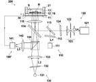
- FIG. 1 is a schematic diagram showing a configuration of a Raman spectroscopic device 100 according to the first embodiment.
- the Raman spectroscopic device 100 includes a photoelectric field enhancement device 10 that supports a subject R in a liquid sample S, and illumination optics that illuminates the subject R on the photoelectric field enhancement device 10 with illumination light L2.
- a light detection unit 120 for detecting from the back side of the photoelectric field enhancement device 10 is provided.
- the photoelectric field enhancement device 10 can move in the substrate in-plane direction (arrow direction in the figure) so that the excitation light L1 is irradiated to the subject arrangement position detected by the position detection unit 140.
- the stage is provided as the position adjusting means, but the mode is not limited to the stage.
- FIG. 1 a mode in which the cell member 21 having a cylindrical side wall portion is provided on the transparent substrate 11 to hold the liquid sample S is shown, but the present invention is not limited to this mode.
- FIG. 2 is a sectional view in the thickness direction of the photoelectric field enhancement device 10 shown in FIG.
- the photoelectric field enhancement device 10 includes a transparent fine uneven structure 12 on a transparent substrate 11 and a fine uneven structure 13 made of gold formed on the transparent fine uneven structure 12, and includes excitation light.
- L1 localized plasmons are induced on the surface, and a photoelectric field enhanced by localized plasmon resonance is generated.
- the fine concavo-convex structure 13 made of gold is not particularly limited as long as the average size and the average pitch of the concavo-convex convex portions can cause localized plasmons on the surface by irradiation with the excitation light L1. It is preferably shorter than the wavelength of the light L1.
- the fine concavo-convex structure 13 made of a gold film preferably has an average depth of 200 nm or less from the top of the convex part to the bottom of the adjacent concave part, and an average pitch between the vertices of the most adjacent convex parts across the concave part of 200 nm or less.
- the average film thickness of the fine concavo-convex structure 13 made of gold is preferably within a range of 10 to 150 nm, and more preferably 30 to 100 nm. Within such a film thickness range, signal light can be transmitted well and a good electric field enhancement effect can be obtained.
- the average film thickness may be considered as the film thickness of the formed gold film. For example, if the film is formed under the same conditions as those when a film is formed on a flat glass substrate, it may be determined that a gold film having a thickness formed on the flat glass substrate is formed.
- the fine concavo-convex structure 13 made of gold may be provided with the fine concavo-convex structure 12 on the base substrate as in this embodiment, and may have a fine concavo-convex structure corresponding to the concavo-convex structure of the base.
- a substrate having a high surface smoothness may be used, and the substrate may have a fine concavo-convex structure independent of the shape of the surface of the base substrate.
- the transparent substrate 11 is not particularly limited as long as it has transparency, but higher transparency is preferable, and examples thereof include glass and acrylic resin.
- the transparent substrate 11 may have a single layer structure or a laminated structure.
- the cell member (liquid holding means) 21 is not particularly limited, but may be formed of the same material as the transparent substrate 11.
- the transparent fine concavo-convex structure 12 is not particularly limited as long as it is a concavo-convex structure (average depth, average pitch) capable of inducing localized plasmons on the surface of the fine concavo-convex structure 13 on the surface of the gold film formed thereon.
- the transparent fine concavo-convex structure 12 is preferably a buyer light layer or a boehmite layer, and is preferably a boehmite layer because the formation method is easy and the in-plane uniformity of the concavo-convex structure is high.
- the in-plane uniformity of the surface uneven structure is high, even if the measurement is performed by changing the light irradiation position on the same sample, the reproducibility is good. Data is obtained. Therefore, a plurality of data can be taken for the same sample by changing the light irradiation location, and the reliability of the data can be increased.
- a plate-like transparent substrate 11 is prepared, and the transparent substrate 11 is washed with pure water. Thereafter, an aluminum layer is formed on the surface of the transparent substrate 11 by a sputtering method to a thickness of about several tens of nanometers.
- the transparent substrate 11 with the aluminum layer is immersed in pure water boiled and taken out after a few minutes (about 5 minutes).
- this boiling treatment boiling treatment
- the aluminum layer becomes transparent, and a transparent fine uneven structure (boehmite layer) 12 is formed.
- gold can be deposited by vapor deposition to obtain the photoelectric field enhancement device 10.
- Gold is not limited to vapor deposition, but may be formed by fixing gold fine particles, for example. Further, the vapor deposition method is not limited to a normal vapor deposition method, and an oblique vapor deposition method may be used.
- the concavo-convex shape of the fine concavo-convex structure 13 made of gold is a shape that conforms to the shape of the concavo-convex structure 12 on the boehmite surface. In this case, the uneven shape is different from the uneven shape of the base.
- Examples of the transparent fine concavo-convex structure 12 include an anodized aluminum film obtained by anodizing aluminum and removing a non-anodized portion.
- the transparent substrate 11 and the transparent fine concavo-convex structure 12 are shown as being formed of different materials.
- the transparent fine substrate 11 is formed by processing the surface of the transparent substrate 11.
- the transparent substrate 11 and the transparent fine concavo-convex structure 12 are integrated.
- Such a configuration can be formed, for example, by subjecting the surface of the glass substrate to lithography and dry etching.
- the excitation light irradiation unit 110 emits the excitation light L1, the laser line filter 112 that uses the light L1 emitted from the excitation light source 111 as excitation light of a specific wavelength, and the excitation light that has passed through the filter 112. From the dichroic mirror 113 that reflects L1 toward the substrate 10, the excitation light L1 reflected by the dichroic mirror 113, and the substrate 10 side that includes enhanced Raman scattered light Ls generated from the subject R by irradiation of the excitation light L1.
- the object R of the photoelectric field enhancement device 10 mounts the hot mirror 114 capable of reflecting the light at the light detection unit 120 side and transmitting the position detection light L3 described later and the excitation light L1 transmitted through the hot mirror 114. And a lens 115 for condensing the light from the subject R side and collimating the light on the placed region.
- the light detection unit 120 is disposed on the back side of the transparent substrate 11 and includes Raman scattered light Ls, absorbs the excitation light L1 out of the light that has been reflected by the hot mirror 114 and then transmitted through the dichroic mirror 113, A notch filter 124 that transmits other light, a slit 122 that removes noise light and collimates the Raman scattered light Ls into the spectroscope 121 and a lens pair 123 are provided. In the spectroscope 121, the incident Raman scattered light Ls is dispersed to obtain a Raman spectrum.
- the photoelectric field enhancing device 10 can effectively induce localized plasmons on the surface of the gold film by irradiating the excitation light L1, and can obtain the photoelectric field enhancing effect by the localized plasmons.
- the Raman scattered light (signal light) Ls generated from the subject R when the subject R is irradiated with the excitation light L1 is enhanced by the photoelectric field enhancement effect, and the Raman scattered light is highly sensitive. Ls can be detected.
- the Raman scattered light Ls generated from the subject R is detected from the back side of the transparent substrate 11
- the surface enhanced Raman scattered light (SERS light) enhanced by the enhanced photoelectric field having the maximum intensity on the surface of the gold film. Can be detected without being shielded by the subject R.
- the Raman spectroscopic device 100 further includes an illumination optical system 130 and a position detection unit 140 so that the subject R can be irradiated with the excitation light L1 with high accuracy.
- the illumination optical system 130 irradiates at least the subject R with illumination light L2 with a wavelength of 400 to 530 nm, an illumination light source 131 such as a xenon lamp, a bandpass filter 132 that transmits light with a wavelength of 400 nm to 530 nm, and And a lens 133 that collimates the illumination light L2.
- an illumination light source 131 such as a xenon lamp
- a bandpass filter 132 that transmits light with a wavelength of 400 nm to 530 nm
- a lens 133 that collimates the illumination light L2.
- the position detection unit 140 reflects the position detection light (scattered light) L3 transmitted through the transparent substrate 11 and converted into parallel light by the lens 115 and then transmitted through the hot mirror 114 to the position detection unit (imaging device) 141. It includes a guiding mirror 143 and a condensing lens 142, and detects the position detection light L3 emitted from the subject R by illumination light on the back side of the transparent substrate 11 (the back side of the photoelectric field enhancement device 10). Position information can be obtained. As already described, based on the position information detected by the position detector 140, the stage 30 is moved in the in-plane direction so that the object R can be irradiated with the excitation light L1 with high accuracy.
- the Raman spectroscopic device 100 can irradiate the subject R with excitation light with high accuracy by controlling the irradiation position of the excitation light L1 based on the obtained position detection information, and improve the measurement accuracy. Can do.
- the photoelectric field enhancement device 10 is fixed, and the photoelectric field enhancement device 10 is moved in the in-plane direction so that the excitation light L1 is irradiated to the position detected by the position detection unit 140. It is good also as an aspect provided with the position adjustment means which can be performed.
- the present inventors have studied a configuration that can suppress the temperature rise of the metal film as much as possible and can detect signal light (Raman scattered light) with high accuracy. As a result, it is possible to achieve such detection by performing position detection using illumination light L2 that can be transmitted well through the gold film and has a large amount of light components in the wavelength range with less interference with the main excitation light wavelength range. I found.
- the present inventor first measured the transmission spectrum of the gold film and examined the transmittance peak wavelength range.
- a device for evaluating a transmission spectrum of a gold film an aluminum film having a thickness of 20 nm was formed on a square glass substrate having a thickness of 0.5 mm and a side of 20 mm, and then immersed in pure water in a boil. After a minute, it is taken out and boehmite is prepared, and gold is deposited with a film thickness of 30 nm.
- a spectroscope manufactured by Hitachi, Ltd .: U-4000 the transmittance is measured in the range of 400 nm to 850 nm and the resolution is 1 nm. Was measured. The result is shown in FIG.
- the transmittance peak wavelength range in FIG. 4 can be a transmittance of 22% or more, which is the bottom value near the wavelength of 850 nm.
- the illumination light L2 is considered to have less influence on the detection accuracy of the signal light Ls enhanced by the effect of the photoelectric field enhancement device 10 when it does not include light in a wavelength range that easily interferes with the excitation light L1.
- the wavelength of the excitation light L1 is longer than 600 nm, particularly when the subject is a biological subject such as a biological tissue, cell, microorganism, mycoplasma, protein, etc., where the fluorescence (noise) from the subject is relatively small. Often use light of Therefore, interference with the excitation light L1 can be suppressed if the light has a wavelength in the range of 430 nm to 510 nm.
- the Raman spectroscopic device 100 by using light in the wavelength range of 430 nm to 510 nm as the illumination light L2, the position of the subject is detected with high accuracy without causing thermal damage to the subject, and good S / N can measure the physical characteristics of the signal light.
- the illumination optical system 130 a light-emitting diode, a semiconductor laser, or the like is used as the illumination light source 131, which eliminates the need for the band-pass filter 132. In addition, these light sources consume less power.
- the line width of the illumination light is as narrow as 10 nm or less, and the illumination light can be concentrated on the transmittance peak of the photoelectric field enhancement device 10, so that the effect of suppressing the temperature rise can be expected.
- speckle noise is a problem with semiconductor lasers, noise removal measures such as passing a diffuser or the like before illumination light irradiation are required.
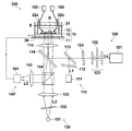
- FIG. 5 is a schematic diagram illustrating a configuration of a Raman spectroscopic device 200 according to the second embodiment. Elements equivalent to the Raman spectroscopic device 100 are denoted by the same reference numerals, and detailed description thereof is omitted.
- the illumination optical system 130 is arranged on the back side of the photoelectric field enhancement device 10.
- the position detection unit 140 reflects the position detection light L3 that has passed through the hot mirror 114 to position detection means (imaging device) 141.
- the position detection unit 140 ′ is provided with a half beam splitter 144 instead of the mirror.
- the illumination optical system 130 is eliminated on the subject side, a terminal from a device for monitoring the environment (temperature, humidity, oxygen concentration, pH, etc.) around the subject is arranged on the subject side, or a reflux cell. It is also easy to obtain a type of photoelectric field enhancement device.
- FIG. 6 shows a configuration of a Raman spectroscopic device 300 including a temperature monitoring device 150 and an oxygen concentration monitoring device 160 as a reflux cell type photoelectric field enhancement device having a liquid inlet 22a and a liquid outlet 22b.
- the Raman spectroscopic device 300 is the same as the Raman spectroscopic device 200 except that the shape of the cell holding the liquid sample S is a reflux cell type and the monitor devices 150 and 160 are provided.
- tube connectors connected to the tubing pumps are fixed to the liquid inlet 22a and the liquid outlet 22b, respectively.
- the liquid around the subject can be circulated by discharging and aspirating the liquid.
- the temperature and oxygen concentration of the liquid can be adjusted when refluxing, the environment around the subject can be maintained or changed to a desired value.
- the temperature around the subject can be controlled by recirculation, local heating on the contact surface of the subject R with the fine concavo-convex structure 13 made of gold cannot be suppressed. Therefore, the position of the subject is detected with high accuracy without causing thermal damage to the subject for the first time by suppressing the temperature rise of the fine concavo-convex structure 13 by the illumination light L3 as a configuration of the Raman spectroscopic device 300, and good S / N can measure the physical characteristics of the signal light.
- the Raman spectroscopic device 300 since the illumination optical system 130 is disposed on the back side of the photoelectric field enhancement device 10, the terminals of the temperature monitoring device 150 and the oxygen concentration monitoring device 160 are disposed near the subject R. be able to. Therefore, since the Raman scattered light can be detected while monitoring the measurement environment around the subject R, a more accurate measurement can be performed while maintaining a good measurement environment. "Design changes"
- the excitation light irradiation part 110 was arrange
- the excitation light irradiation part 110 is It is good also as a structure arrange
- positioning surface side) of the photoelectric field enhancement device 10 and irradiating excitation light from the surface side.
- the fine metal concavo-convex structure of the photoelectric field enhancement device localized plasmon resonance can be similarly induced regardless of whether excitation light is incident from either of the front and back sides, and a photoelectric field enhancement effect can be obtained.
- the photoelectric field enhancement device 10 may have a mode in which a transparent second fine concavo-convex structure layer is provided on the back surface side.
- a transparent second fine concavo-convex structure layer By providing the transparent second fine concavo-convex structure layer, it functions as an antireflection film when irradiated with light.
- the second fine concavo-convex structure layer can be the same as the transparent fine concavo-convex structure layer 12 provided on the surface side of the transparent substrate 10, and is preferably composed of a boehmite layer.
- the aspect of the Raman spectroscopic device in which the light Ls detected by the light detection unit 120 is Raman scattered light has been described.
- the detected light Ls is fluorescence, higher-order harmonics, Rayleigh scattered light, or The same effect can be obtained even in a measuring apparatus that uses Mie scattered light or the like.
Landscapes
- Physics & Mathematics (AREA)
- Spectroscopy & Molecular Physics (AREA)
- General Physics & Mathematics (AREA)
- Health & Medical Sciences (AREA)
- Nuclear Medicine, Radiotherapy & Molecular Imaging (AREA)
- Life Sciences & Earth Sciences (AREA)
- Chemical & Material Sciences (AREA)
- Analytical Chemistry (AREA)
- Biochemistry (AREA)
- General Health & Medical Sciences (AREA)
- Immunology (AREA)
- Pathology (AREA)
- Investigating, Analyzing Materials By Fluorescence Or Luminescence (AREA)
Description
本発明は、局在プラズモンを誘起しうる微細な金属凹凸構造を備えた光電場増強デバイスを用いて増強された信号光を検出してその物理特性を測定する測定装置に関するものである。
金属表面における局在プラズモン共鳴現象による電場増強効果を利用したセンサデバイスやラマン分光用デバイス等の電場増強デバイスが知られている。ラマン分光法は、物質に単波長光を照射して得られる散乱光を分光して、ラマン散乱光のスペクトル(ラマンスペクトル)を得る方法であり、物質の同定等に利用されている。
ラマン分光法には、微弱なラマン散乱光を増強するために、表面増強ラマン(SERS)と呼ばれる、局在プラズモン共鳴によって増強された光電場を利用したラマン分光法がある(非特許文献1参照)。これは、金属体、特に表面にナノオーダの凹凸を有する金属体に物質を接触させた状態で光を照射すると、局在プラズモン共鳴による光電場増強が生じ、金属体表面に接触された試料のラマン散乱光強度が増強されるという原理を利用するものである。被検体を担持する担体(基板)として、表面に金属凹凸構造を備えた基板を用いることにより表面増強ラマン分光法を実施することができる。
表面に金属微細凹凸構造を備えた基板としては、Si基板の表面に凹凸を設け、その凹凸面に金属膜を形成した基板が主に用いられている(特許文献1~3参照)。
また、Al基板の表面を陽極酸化して一部を金属酸化物層(Al2O3)とし、陽極酸化の過程で金属酸化物層内部に自然形成され、金属酸化物層の表面において開口した複数の微細孔内に、金属が充填された基板も提案されている(特許文献4参照)。
特許文献1~4等に開示されている従来の光電場増強デバイスは、SiあるいはAlなどの不透明な基板表面に微細凹凸構造を形成し、その微細凹凸構造表面に金属膜を形成した、あるいは、凹部に金属を埋め込んだ構成である。また、特許文献4にはガラス基板のような透明基板を用いる例が挙げられているが、微細凹凸構造自体はシリコンあるいはゲルマニウムなどの不透明な材料から構成されている。
従来のラマン分光装置においては、サンプル表面側からラマン散乱光を検出するよう構成されている。しかしながら、細胞などのμmオーダー以上のサンプルを被検体とする場合、サンプル自身がラマン散乱光に対する遮蔽体となり、微弱なラマン散乱光を高いS/Nで受光するのは困難であった。
本発明者らは、良好なS/NでSERS計測を実施できる光電場増強デバイスとして、ベーマイトと呼ばれる透明微細凹凸構造の凹凸表面を、金等の金属膜で覆った光電場増強デバイスを開発し、サンプルの裏面側からラマン散乱光を検出可能とすることにより、被検体により遮蔽されることなくプラズモン増強光電場により増強された信号光を検出することができる(特許文献5、特許文献6)。
Optics Express Vol.17, No.2118556
SERS検出を行う際、励起光の焦点を被検体に合わせる必要があり、その被検体の位置検出には、被検体が載置された光電場増強デバイスを照明する必要がある。
位置検出は、被検体の厚みが厚い場合や、被検体が液体試料中にある場合に被検体の精度の良い検出が困難となるため、信号光の検出と同様に、裏面側から実施することが好ましいと考えられる。
しかしながら、特許文献5、特許文献6に記載の光電場増強デバイスは、表面に金属膜を備えているため、照明光の反射や吸収等による損失により、位置検出器に検出される光量が少なくなるという問題がある。また、検出光量を上げるために照明強度を高くすると、金属膜の照明光の吸収により金属膜が昇温し、被検体に熱ダメージを与えてしまう虞がある。特に細胞その代謝物などの生物被検体の場合には、熱刺激によって変性やアポトーシスを引き起こし、死滅させる虞もあることから、できるだけ金属膜の昇温は少ないことが望ましい。
本発明は、上記事情に鑑みてなされたものであって、局在プラズモンによる光増強効果を利用して微弱な光を増強し検出する測定方法および装置において、被検体に熱ダメージを与えることなく高精度な被検体の位置検出が可能であり、良好なS/Nで信号光の物理特性を測定することが可能な光測定装置を提供することを目的とする。
本発明の測定装置は、透明基板と、この透明基板の表面に形成された、励起光の照射により局在プラズモンを誘起しうる金からなる微細凹凸構造とを備え、この微細凹凸構造表面に被検体が配置される光電場増強デバイスと、
少なくとも被検体に波長430~510nmの照明光を照射する照明光学系と
光電場増強デバイスの裏面側に配置された、照明光が照射された被検体から発せられる光を透明基板の裏面側から検出して被検体の位置を検出する位置検出部と、
位置検出部により検出された位置に、励起光を照射する励起光照射部と、
光電場増強デバイスの裏面側に配置された、前記励起光の照射により被検体から発せられる信号光を透明基板の裏面側から検出する光検出部とを備えたことを特徴とするものでる。
少なくとも被検体に波長430~510nmの照明光を照射する照明光学系と
光電場増強デバイスの裏面側に配置された、照明光が照射された被検体から発せられる光を透明基板の裏面側から検出して被検体の位置を検出する位置検出部と、
位置検出部により検出された位置に、励起光を照射する励起光照射部と、
光電場増強デバイスの裏面側に配置された、前記励起光の照射により被検体から発せられる信号光を透明基板の裏面側から検出する光検出部とを備えたことを特徴とするものでる。
ここで、透明とは、前記微細凹凸構造に照射される光、および該光により被検体から生じる光、照明光に対し、透過率が50%以上であることをいうものとする。なお、これらの光に対して、透過率は75%以上、さらには90%以上であることが好ましい。
また、波長400~530nmの照明光とは、光電場増強デバイス10の一表面側から照明光を照射した際に、裏面側に透過してくる全光量(可視領域400~750nm)のうち、40%以上がこの波長範囲内の光である照明光を意味する。
また、金からなる微細凹凸構造の平均膜厚は、10~150nmの範囲内であることが好ましい。
また、金からなる微細凹凸構造は、下地基材に微細凹凸構造を備え、下地の凹凸構造に応じた微細凹凸構造を有するものであってもよいし、下地基材の表面の形状によらない微細凹凸構造を有するものであってもよい。
局在プラズモンを生じうる微細凹凸構造とは、一般に、凹凸構造をなす凸部および凹部の平均的な大きさと平均的なピッチが光の波長よりも小さい凹凸構造である。
特には、凹凸の平均的なピッチおよび凸部の頂点と凹部の底部間の距離(深さ)が200nm以下であることが好ましい。
凹凸の平均的なピッチは、SEM(走査型電子顕微鏡)で微細凹凸構造の表面画像を撮影し、画像処理をして2値化し、統計的処理によって求めるものとする。
凹凸の平均的な深さは、AFM(原子間力顕微鏡)により表面形状を測定して統計的処理によって求めるものとする。
光電場増強デバイスの好ましい態様としては、表面に微細凹凸構造を備えた透明基板と、この透明基板の表面に形成された金膜とを備える。かかる態様の透明基板としては、少なくとも微細凹凸構造がバイヤーライト又はベーマイトであることが好ましい。
照射光学系は、光電場増強デバイスの裏面側に配置されてなる態様が好ましい。
励起光照射部は、光電場増強デバイスの裏面側に配置され、透明基板の裏面側から励起光を照射するものである態様が好ましい。
透明な微細凹凸構造の主成分は、金属水酸化物又は金属酸化物の水酸化物であることが好ましい。本明細書において「主成分」とは、含量90質量%以上の成分を意味する。
本発明の測定装置は、光電場増強デバイスが、金からなる微細凹凸構造上に液体試料を保持するための液体試料保持部材を備えた態様にも好適に用いられる。かかる態様において、液体試料保持部材が、液体の流入部および流出部を備えていてもよい。
また、光電場増強デバイスが固定されてなり、位置検出部により検出された位置に励起光が照射されるように光電場増強デバイスを面内方向に移動させることができる位置調整手段を備えてなる態様が好ましい。
光検出部により検出する光としては、ラマン散乱光、表面増強ラマン散乱光、蛍光、高次高調波、レーリー散乱光あるいはミー散乱光等が挙げられ、ラマン散乱光又は表面増強ラマン散乱光が好適である。
本発明の測定装置は、被検体が、生体組織、細胞、微生物、マイコプラズマ、タンパク質等の生物被検体に好適に用いることができる。
本発明の測定装置は、局在プラズモンを誘起しうる金からなる微細凹凸構造を表面に備えた光電場増強デバイス上に被検体を載置し、少なくとも被検体を波長400~530nmの光で照明して、光電場増強デバイスの裏面側に配置された位置検出部により被検体の位置を検出し、その位置に、励起光を照射して、裏面側からこの照射により被検体から発せられる信号光を透明基板の裏面側から検出する構成としている。
光電場増強デバイスは、励起光を照射することにより、金からなる微細凹凸構造の表面に局在プラズモンを効果的に誘起することができ、この局在プラズモンによる光電場増強効果を得ることができる。従って、被検体に光が照射されることにより、被検体から生じる信号光は光電場増強効果により増強されたものとなり、高感度に信号光を検出することができる。
本発明では、金膜を良好に透過可能、且つ、主な励起光及び信号光の波長範囲と干渉の少ない波長範囲の光成分が多い照明光を用いて位置検出を行って、光電場増強デバイスの効果により増強された信号光を検出することができる。また、被検体から生じた光(検出光)を、透明基板の裏面側から検出するので、金属膜の表面において最大強度を有する増強光電場により増強された光を、被検体により遮蔽されることなく検出することができる。従って、被検体に熱ダメージを与えることなく高精度に被検体の位置検出を行い、良好なS/Nで信号光の物理特性を測定することができる。
以下、図面を参照して本発明の測定方法および測定装置の実施形態について説明する。なお、視認しやすくするため、図面中の各構成要素の縮尺等は実際のものとは適宜異ならせてある。
(第1の実施形態)
本発明の測定装置の第1の実施形態として、ラマン分光装置100について説明する。図1は、第1の実施形態に係るラマン分光装置100の構成を示す概略図である。
本発明の測定装置の第1の実施形態として、ラマン分光装置100について説明する。図1は、第1の実施形態に係るラマン分光装置100の構成を示す概略図である。
図1に示すように、ラマン分光装置100は、液体試料S中の被検体Rを支持する光電場増強デバイス10と、光電場増強デバイス10上の被検体Rを照明光L2により照明する照明光学系130と、照明光L2により照明された被検体から発せられる光を透明基板の裏面側から検出して被検体Rの位置を検出する位置検出部140と、光電場増強デバイス10の裏面側(透明基板側)から被検体配置位置へ励起光L1を照射する励起光照射部110と、被検体Rから発せられ光電場増強デバイス10の作用により増強されたラマン散乱光(信号光)Lsを、光電場増強デバイス10の裏面側から検出するための光検出部120を備えている。
ラマン分光装置100では、位置検出部140より検出された被検体配置位置へ励起光L1が照射されるように、光電場増強デバイス10は、基板面内方向(図中矢印方向)に移動可能とする透明なステージ(位置調整手段)30上に載置されている。本実施形態において、ステージを位置調整手段として設けているが、その態様はステージに限定されない。
まず、光電場増強デバイス10について説明する。図1では、透明基板11上に筒状の側壁部を有するセル部材21を設けて液体試料Sを保持可能な態様について示してあるが、この態様に限定されるものではない。
図2は、図1に示した光電場増強デバイス10の厚み方向断面図である。図視されるように、光電場増強デバイス10は、透明基板11上に、透明微細凹凸構造12と、透明微細凹凸構造12上に形成された金からなる微細凹凸構造13とからなり、励起光L1の照射により、表面に局在プラズモンが誘起されて、局在プラズモン共鳴により増強された光電場を生じさせるものである。
金からなる微細凹凸構造13は、その凹凸の凸部の平均的な大きさおよび平均ピッチは、励起光L1の照射により表面において局在プラズモンを生じさせうるものであれば特に限定されないが、励起光L1の波長より短いことが好ましい。金膜からなる微細凹凸構造13は、凸部頂点から隣接する凹部の底部までの平均深さが200nm以下、凹部を隔てた最隣接凸部の頂点同士の平均ピッチが200nm以下であることが望ましい。
金からなる微細凹凸構造13の平均膜厚は、10~150nmの範囲内であることが好ましく、30~100nmがより好ましい。かかる膜厚範囲であれば、信号光を良好に透過し、且つ、良好な電場増強効果を得ることができる。なお、透明微細凹凸構造上に金膜を成膜してなる微細凹凸構造13の場合は、平均膜厚は、成膜した金膜の膜厚と考えてよい。例えば、平らなガラス基板上に成膜する場合と同条件での成膜であれば、平らなガラス基板上に成膜される厚みの金膜が成膜されると判断してよい。
金からなる微細凹凸構造13は、本実施形態のように下地基材に微細凹凸構造12を備え、下地の凹凸構造に応じた微細凹凸構造を有するものであってもよいし、下地基材に表面平滑性の高い基材を用い、下地基材の表面の形状によらない微細凹凸構造を有するものであってもよい。
透明基板11は、透明性を有していれば特に制限されないが、透明性が高い方が好ましく、例えばガラスやアクリル樹脂等が挙げられる。透明基板11は単層構造であっても積層構造であってもよい。セル部材(液体保持手段)21については特に制限されないが、透明基板11と同じ材料により形成してもよい。
透明微細凹凸構造12としては、その上に成膜される金膜の表面の微細凹凸構造13の表面において局在プラズモンが誘起されうる凹凸構造(平均深さ、平均ピッチ)であれば特に制限されない。透明微細凹凸構造12としては、バイヤーライト層又はベーマイト層が好ましく、形成方法が容易であり、凹凸構造の面内均一性が高いことからベーマイト層であることが最も好ましい。ベーマイトを用いた光電場増強デバイス10を用いた態様では、表面凹凸構造の面内均一性が高いので、同一試料に対して、光照射箇所を変えて測定を実施しても、再現性のよいデータが得られる。したがって、同一試料に対して、光照射箇所を変えて複数のデータを取り、データの信頼性を上げることが可能である。
光電場増強デバイス10の製造方法の一例として、透明微細凹凸構造12としてベーマイト層を備えた態様について説明する。
まず板状の透明基板11を用意し、透明基板11を純水洗浄する。その後、透明基板11の表面にスパッタ法によりアルミニウム層を数十nm程度成膜する。
次いで、純水を沸騰させた中に、アルミニウム層付き透明基板11を浸水させ、数分(5分程度)後に取り出す。この煮沸処理(ベーマイト処理)により、アルミニウム層は透明化し、透明微細凹凸構造(ベーマイト層)12が形成される。
得られたベーマイト層12上に、金を蒸着により成膜し、光電場増強デバイス10を得ることができる。なお、金は、蒸着に限らず、たとえば金の微粒子を固定化して形成するようにしてもよい。また、蒸着法についても、通常の蒸着法に限らず、斜め蒸着法を用いてもよい。ベーマイト層12の上に金を成膜した場合、金からなる微細凹凸構造13の凹凸形状は、ベーマイト表面の凹凸構造12の形状に沿った形状となると通常は考えられるが、金は凝集等を生じやすいことから、その場合はその凹凸形状は下地の凹凸形状とは異なる態様となる。
透明微細凹凸構造12としては、その他にアルミニウムを陽極酸化した後に非陽極酸化部分を除去して得られる陽極酸化アルミニウム皮膜等が例示される。また、本実施形態では透明基板11と透明微細凹凸構造12とが異なる材料により構成された態様について示してあるが、透明基板11の表面を加工して透明微細凹凸構造12を形成した態様であってもよく、この場合は、透明基板11と透明微細凹凸構造12とが一体化されてなる構成となる。かかる構成は、例えば、ガラス基板の表面をリソグラフィーとドライエッチング処理することにより形成することができる。
励起光照射部110は、励起光L1を射出する励起光源111と、この励起光源111から射出された光L1を特定の波長の励起光とするレーザーラインフィルタ112と、フィルタ112を通過した励起光L1を基板10側へ反射するダイクロイックミラー113と、該ダイクロイックミラー113により反射された励起光L1と該励起光L1の照射により被検体Rから生じ増強されたラマン散乱光Lsを含む基板10側からの光を光検出部120側へ反射させ、後記する位置検出光L3を透過することができるホットミラー114と、ホットミラー114を透過した励起光L1を光電場増強デバイス10の被検体Rが載置された領域に集光すると共に、被検体R側からの光を平行光化するレンズ115とを備えている。
光検出部120は、透明基板11の裏面側に配置されてなり、ラマン散乱光Lsを含み、ホットミラー114により反射された後にダイクロイックミラー113を透過してきた光のうち励起光L1を吸収し、それ以外の光を透過するノッチフィルタ124と、ノイズ光を除去して分光器121にラマン散乱光Lsを平行光化して入射させるスリット122及びレンズ対123を備えている。分光器121では、入射されたラマン散乱光Lsが分光されてラマンスペクトルが得られる。
光電場増強デバイス10は、励起光L1を照射することにより、金膜の表面に局在プラズモンを効果的に誘起することができ、この局在プラズモンによる光電場増強効果を得ることができる。ラマン分光装置100では、被検体Rに励起光L1が照射されることにより被検体Rから生じるラマン散乱光(信号光)Lsは光電場増強効果により増強されたものとなり、高感度にラマン散乱光Lsを検出することができる。
また、被検体Rから生じたラマン散乱光Lsを、透明基板11の裏面側から検出するので、金膜の表面において最大強度を有する増強光電場により増強された表面増強ラマン散乱光(SERS光)を、被検体Rにより遮蔽されることなく検出することができる。
ラマン分光装置100では、更に、被検体Rに精度良く励起光L1を照射可能とするために、照明光学系130及び位置検出部140を備えている。
照明光学系130は、少なくとも被検体Rに波長400~530nmの照明光L2を照射するものであり、キセノンランプ等の照明光源131と、波長400nm~530nmの光を透過するバンドパスフィルタ132と、照明光L2を平行光化するレンズ133とを備えている。
光電場増強デバイス10上の被検体Rをレンズ133を通過した照明光L2により照明すると、照明光L2により被検体Rから発せられた光の一部が透明基板11側に光L3として透過する。
位置検出部140は、透明基板11を透過し、レンズ115により平行光化された後に、ホットミラー114を透過した位置検出光(散乱光)L3を反射させて位置検出手段(撮像素子)141に導くミラー143と集光レンズ142を備えており、照明光により被検体Rから発せられる位置検出光L3を透明基板11の裏面側(光電場増強デバイス10の裏面側)において検出して被検体Rの位置情報を得ることができる。既に述べたように、位置検出部140により検出された位置情報に基づいて、ステージ30を面内方向に移動させ、励起光L1を精度良く被検体Rへの照射可能としている。
ラマン分光装置100では、得られた位置検出情報に基づいて、励起光L1の照射位置を制御することにより、高精度に被検体Rに励起光を照射することができ、測定精度を向上させることができる。本実施形態において、光電場増強デバイス10が固定されてなり、位置検出部140により検出された位置に励起光L1が照射されるように、光電場増強デバイス10を面内方向に移動させることができる位置調整手段を備えてなる態様としてもよい。
「発明が解決しようとする課題」の項目において述べたように、SERS光検出を行う際、励起光の焦点を被検体に合わせる必要があるが、光電場増強デバイス10のように、表面に金属膜を備えたデバイスを被検体の保持に用いる場合、その被検体の位置検出に用いる照明光の反射や吸収等による損失により、位置検出器に検出される光量が少なくなるという問題があり、検出光量を上げるために照明強度を高くすると、金属膜の照明光の吸収により金属膜が昇温し、被検体に熱ダメージを与えてしまう虞があることを述べた。
本発明者らは、金属膜の昇温をできるだけ抑制し、且つ、高精度な信号光(ラマン散乱光)の検出を実施可能な構成について検討を行った。その結果、金膜を良好に透過可能、且つ、主な励起光波長範囲と干渉の少ない波長範囲の光成分が多い照明光L2を用いて位置検出を実施することによりかかる検出を実現しうることを見出した。
本発明者は、まず、金膜の透過スペクトルを測定し、透過率ピーク波長範囲を調べた。金膜の透過スペクトル評価用デバイスとして、厚み0.5mm,一辺が20mmの正方形のガラス基板上に、アルミニウムを20nmの膜厚で成膜した後、純水を沸騰させた中に浸水させて5分後に取り出してベーマイト化し、その上に、金を30nmの膜厚で蒸着したものを用意し、日立製作所製分光器:U-4000を用いて、測定範囲400nm~850nm、分解能1nmにて透過率を測定した。その結果を図4に示す。透過率ピーク波長範囲は、図4において、波長850nm付近のボトム値である透過率22%以上となりうるものとした。
次に、信号光検出の精度への影響について検討した。照明光L2としては、励起光L1と干渉しやすい波長範囲の光を含まない方が、光電場増強デバイス10の効果により増強された信号光Lsの検出精度への影響は少ないと考えられる。
励起光L1の波長は、特に、被検体が、生体組織、細胞、微生物、マイコプラズマ、タンパク質等の生物被検体である場合、被検体からの蛍光(ノイズ)が比較的小さい600nmよりも長波長側の光を用いることが多い。従って、波長430nm~510nmの範囲の光であれば、励起光L1との干渉をも抑制可能である。
従って、ラマン分光装置100において、照明光L2として、波長430nm~510nmの範囲の光を用いることにより、被検体に熱ダメージを与えることなく高精度に被検体の位置検出を行い、良好なS/Nで信号光の物理特性を測定することができる。
なお、照明光学系130としては、照明光源131として発光ダイオードや半導体レーザ等を用いることにより、バンドパスフィルター132が不要となり、省スペース、低コスト化の点で好ましい。また、これらの光源は消費電力も少なくて済む。
また、半導体レーザの場合は、照明光の線幅が10nm以下と狭く、照明光を光電場増強デバイス10の透過率ピークに集中させることが可能なため、より昇温を抑制する効果が期待できる。ただし、半導体レーザはスペックルノイズが問題となるため、照明光照射前にディフューザー等を通過させる等のノイズ除去対策が必要となる。
(第2の実施形態)
本発明の測定装置の第2の実施形態として、ラマン分光装置200について説明する。図5は、第2の実施形態に係るラマン分光装置200の構成を示す概略図である。ラマン分光装置100と同等の要素には同一符号を付し、詳細な説明は省略する。
本発明の測定装置の第2の実施形態として、ラマン分光装置200について説明する。図5は、第2の実施形態に係るラマン分光装置200の構成を示す概略図である。ラマン分光装置100と同等の要素には同一符号を付し、詳細な説明は省略する。
図5に示されるラマン分光装置200は、照明光学系130が光電場増強デバイス10の裏面側に配置されている。照明光学系130が被検体R側に配置されていた第1の実施形態においては、位置検出部140は、ホットミラー114を透過した位置検出光L3を反射させて位置検出手段(撮像素子)141に導くミラー143を備えた構成としていたが、本実施形態では、位置検出部140’は、ミラーの代わりにハーフビームスプリッタ144を備えた態様としている。
かかる構成とすることにより、第1の実施形態に比して、被検体Rやその周辺環境(液体試料等)による照明光L2の吸収を抑制し、被検体Rへの光ダメージや温度刺激をより低減させることができる。
また、被検体側に照明光学系130がなくなることで、被検体周辺の環境(温度、湿度、酸素濃度、pHなど)をモニターする装置からの端子を被検体側に配置することや、環流セル型の光電場増強デバイスとすることも容易となる。
図6は、液体流入口22a及び液体流出口22bを備えた環流セル型の光電場増強デバイスとし、温度モニター装置150及び酸素濃度モニター装置160を備えたラマン分光装置300の構成を示す。ラマン分光装置300において、液体試料Sを保持するセルの形状を環流セル型とし、モニター装置150及び160を備えている以外はラマン分光装置200と同様である。
環流セル型とする場合は、液体流入口22a及び液体流出口22bには、図示していないが、それぞれチュービングポンプに接続されるチューブコネクタが固定されている。環流セル型とすれば、液体を排出、吸引することで被検体周辺の液体を環流させることができる。
環流させる際に液体の温度や酸素濃度を調整することができるため、被検体周辺の環境を所望の値に維持又は変化させることができる。しかしながら、環流によって被検体周辺の温度制御が可能となっても、被検体Rにおいて、金からなる微細凹凸構造13との接触面における局所的な加熱は抑制することができない。従って、ラマン分光装置300の構成として照明光L3による微細凹凸構造13の昇温を抑制することによってはじめて被検体に熱ダメージを与えることなく高精度に被検体の位置検出を行い、良好なS/Nで信号光の物理特性を測定することができる。
更に、ラマン分光装置300では、照明光学系130を光電場増強デバイス10の裏面側に配置していることから、温度モニター装置150や酸素濃度モニター装置160の端子を被検体Rの近くに配置することができる。従って、被検体R周辺の測定環境をモニタリングしながらラマン散乱光の検出ができるため、良好な測定環境を維持してより高精度な測定を実施することができる。
「設計変更」
「設計変更」
上記実施形態において、励起光照射部110は光検出部120と共に、光電場増強デバイス10の裏面側に配置され、裏面側から励起光を照射する構成について説明したが、励起光照射部110は、光電場増強デバイス10の表面側(被検体配置面側)に配置し、表面側から励起光を照射する構成としてもよい。光電場増強デバイスの金属微細凹凸構造に対しては、表裏のいずれから励起光が入射されても同様に局在プラズモン共鳴を誘起することができ、光電場増強効果を得ることができる。
また、光電場増強デバイス10は、裏面側に、透明な第2の微細凹凸構造層を備えた態様としてもよい。透明な第2の微細凹凸構造層を設けることにより、光が照射された際に反射防止膜として機能する。第2の微細凹凸構造層は、透明基板10の表面側に設けられた透明微細凹凸構造層12と同様のものとすることができ、ベーマイト層により構成することが好ましい。
また、上記実施形態においては、光検出部120により検出する光Lsがラマン散乱光であるラマン分光装置の態様について説明したが、検出する光Lsが、蛍光、高次高調波、レーリー散乱光あるいはミー散乱光等であるような測定装置においても、同様の効果を得ることができる。
Claims (12)
- 透明基板と、該透明基板の表面に形成された、励起光の照射により局在プラズモンを誘起しうる金からなる微細凹凸構造とを備え、該微細凹凸構造表面に被検体が配置される光電場増強デバイスと、
少なくとも前記被検体に波長400~530nmの照明光を照射する照明光学系と
前記光電場増強デバイスの裏面側に配置された、前記照明光が照射された前記被検体から発せられる光を前記透明基板の裏面側から検出して前記被検体の位置を検出する位置検出部と、
前記光電場増強デバイスの前記位置に励起光を照射する励起光照射部と、
前記光電場増強デバイスの裏面側に配置された、前記励起光の照射により前記被検体から発せられる信号光を、前記透明基板の裏面側から検出する光検出部とを備えたことを特徴とする測定装置。 - 前記照射光学系が、前記光電場増強デバイスの裏面側に配置されてなることを特徴とする請求項1に記載の測定装置。
- 前記励起光照射部が、前記光電場増強デバイスの裏面側に配置され、前記透明基板の裏面側から前記励起光を照射するものであること特徴とする請求項1又は2に記載の測定装置。
- 前記光電場増強デバイスが、表面に微細凹凸構造を備えた透明基板と、該透明基板の表面に形成された金からなる微細凹凸構造とを備えてなることを特徴とする請求項1~3のいずれかに記載の測定装置。
- 前記透明基板の主成分が金属水酸化物又は金属酸化物の水酸化物であることを特徴とする請求項4に記載の測定装置。
- 前記透明基板の少なくとも微細凹凸構造がバイヤーライト又はベーマイトからなることを特徴とする請求項5に記載の測定装置。
- 前記金からなる微細凹凸構造膜の平均膜厚が10~100nmであることを特徴とする請求項1~6のいずれかに記載の測定装置。
- 前記光電場増強デバイスが、前記透明基板の前記金からなる微細凹凸構造上に液体試料を保持するための液体試料保持部材を備えてなることを特徴とする請求項1~7のいずれかに記載の測定装置。
- 前記光電場増強デバイスの前記液体試料保持部材が、液体の流入部および流出部を備えてなることを特徴とする請求項8に記載の測定装置。
- 前記光電場増強デバイスが固定されてなり、前記位置検出部により検出された前記位置に前記励起光が照射されるように前記光電場増強デバイスを面内方向に移動させることができる位置調整手段を備えてなること特徴とする請求項1~9のいずれかに記載の測定装置。
- 前記光検出部により検出する光が、ラマン散乱光又は表面増強ラマン散乱光であることを特徴とする請求項1~10のいずれかに記載の測定装置。
- 前記被検体が、生体組織、細胞、微生物、マイコプラズマ、タンパク質のいずれかであることを特徴とする請求項1~11のいずれかに記載の測定装置。
Priority Applications (1)
| Application Number | Priority Date | Filing Date | Title |
|---|---|---|---|
| US14/668,500 US9791375B2 (en) | 2012-09-28 | 2015-03-25 | Light measuring apparatus employing optical electric field enhancing device |
Applications Claiming Priority (2)
| Application Number | Priority Date | Filing Date | Title |
|---|---|---|---|
| JP2012215406A JP5947181B2 (ja) | 2012-09-28 | 2012-09-28 | 光電場増強デバイスを用いた光測定装置 |
| JP2012-215406 | 2012-09-28 |
Related Child Applications (1)
| Application Number | Title | Priority Date | Filing Date |
|---|---|---|---|
| US14/668,500 Continuation US9791375B2 (en) | 2012-09-28 | 2015-03-25 | Light measuring apparatus employing optical electric field enhancing device |
Publications (1)
| Publication Number | Publication Date |
|---|---|
| WO2014050132A1 true WO2014050132A1 (ja) | 2014-04-03 |
Family
ID=50387564
Family Applications (1)
| Application Number | Title | Priority Date | Filing Date |
|---|---|---|---|
| PCT/JP2013/005754 Ceased WO2014050132A1 (ja) | 2012-09-28 | 2013-09-27 | 光電場増強デバイスを用いた光測定装置 |
Country Status (3)
| Country | Link |
|---|---|
| US (1) | US9791375B2 (ja) |
| JP (1) | JP5947181B2 (ja) |
| WO (1) | WO2014050132A1 (ja) |
Families Citing this family (2)
| Publication number | Priority date | Publication date | Assignee | Title |
|---|---|---|---|---|
| US10866189B2 (en) | 2015-11-24 | 2020-12-15 | Hitachi, Ltd. | Optical measurement apparatus and optical measurement method |
| WO2025115175A1 (ja) * | 2023-11-30 | 2025-06-05 | メタセンシング株式会社 | 顕微分光装置 |
Citations (3)
| Publication number | Priority date | Publication date | Assignee | Title |
|---|---|---|---|---|
| JPH0972848A (ja) * | 1995-09-04 | 1997-03-18 | Jasco Corp | ラマン分光装置 |
| WO2010016267A1 (ja) * | 2008-08-08 | 2010-02-11 | 独立行政法人科学技術振興機構 | 粒子プローブ近傍に存在する物質の分布を検出する方法、粒子プローブを用いた画像化方法およびその利用 |
| JP2012063294A (ja) * | 2010-09-17 | 2012-03-29 | Fujifilm Corp | 光電場増強デバイスを用いた光の測定方法および測定装置 |
Family Cites Families (9)
| Publication number | Priority date | Publication date | Assignee | Title |
|---|---|---|---|---|
| US6970239B2 (en) | 2002-06-12 | 2005-11-29 | Intel Corporation | Metal coated nanocrystalline silicon as an active surface enhanced Raman spectroscopy (SERS) substrate |
| US7361313B2 (en) | 2003-02-18 | 2008-04-22 | Intel Corporation | Methods for uniform metal impregnation into a nanoporous material |
| JP4163606B2 (ja) | 2003-12-10 | 2008-10-08 | 富士フイルム株式会社 | 微細構造体、微細構造体の作製方法、ラマン分光方法および装置 |
| JP2006145230A (ja) | 2004-11-16 | 2006-06-08 | Canon Inc | 被分析物担体およびその製造方法 |
| WO2008100582A2 (en) * | 2007-02-14 | 2008-08-21 | Chemimage Corporation | Spectroscopic system and method for predicting outcome of disease |
| US8836941B2 (en) * | 2010-02-10 | 2014-09-16 | Imra America, Inc. | Method and apparatus to prepare a substrate for molecular detection |
| US8159665B2 (en) * | 2010-07-21 | 2012-04-17 | Bwt Property, Inc. | Apparatus and methods for fluorescence subtraction in Raman spectroscopy |
| JP5552007B2 (ja) | 2010-09-17 | 2014-07-16 | 富士フイルム株式会社 | 光電場増強デバイス |
| US8873038B2 (en) * | 2010-10-27 | 2014-10-28 | The Board Of Trustees Of The University Of Illinois | Tailored raman spectrocopic probes for ultrasensitive and highly multiplexed assays |
-
2012
- 2012-09-28 JP JP2012215406A patent/JP5947181B2/ja not_active Expired - Fee Related
-
2013
- 2013-09-27 WO PCT/JP2013/005754 patent/WO2014050132A1/ja not_active Ceased
-
2015
- 2015-03-25 US US14/668,500 patent/US9791375B2/en not_active Expired - Fee Related
Patent Citations (3)
| Publication number | Priority date | Publication date | Assignee | Title |
|---|---|---|---|---|
| JPH0972848A (ja) * | 1995-09-04 | 1997-03-18 | Jasco Corp | ラマン分光装置 |
| WO2010016267A1 (ja) * | 2008-08-08 | 2010-02-11 | 独立行政法人科学技術振興機構 | 粒子プローブ近傍に存在する物質の分布を検出する方法、粒子プローブを用いた画像化方法およびその利用 |
| JP2012063294A (ja) * | 2010-09-17 | 2012-03-29 | Fujifilm Corp | 光電場増強デバイスを用いた光の測定方法および測定装置 |
Also Published As
| Publication number | Publication date |
|---|---|
| JP2014070928A (ja) | 2014-04-21 |
| US20150198535A1 (en) | 2015-07-16 |
| JP5947181B2 (ja) | 2016-07-06 |
| US9791375B2 (en) | 2017-10-17 |
Similar Documents
| Publication | Publication Date | Title |
|---|---|---|
| JP5552007B2 (ja) | 光電場増強デバイス | |
| JP5553717B2 (ja) | 光電場増強デバイスを用いた光の測定方法および測定装置 | |
| JP5848013B2 (ja) | 光電場増強デバイスおよび該デバイスを備えた測定装置 | |
| JP6461904B2 (ja) | 表面増強電場を用いた欠陥検出 | |
| US8587786B2 (en) | Method for high-resolution detection of nanoparticles on two-dimensional detector surfaces | |
| JP2013511041A (ja) | 減衰全反射に基づいた光センサシステムおよび感知方法 | |
| EP3574351A1 (en) | A plasmonic device | |
| US20140242573A1 (en) | Optical element, analysis device, analysis method and electronic apparatus | |
| US9304087B2 (en) | Raman spectroscopic apparatus, raman spectroscopic method, and electronic apparatus | |
| Su et al. | Measurements of light scattering in an integrated microfluidic waveguide cytometer | |
| JP5947181B2 (ja) | 光電場増強デバイスを用いた光測定装置 | |
| WO2013080505A1 (ja) | センシング装置およびこれを用いたセンシング方法 | |
| WO2015146036A1 (ja) | 増強ラマン分光装置 | |
| Zhang et al. | A planar plasmonic nano-gap and its array for enhancing light-matter interactions at the nanoscale | |
| JP5947182B2 (ja) | 光電場増強デバイスを用いた測定装置 | |
| JP6414407B2 (ja) | ラマン分光装置、および電子機器 | |
| JP7361338B2 (ja) | 検出装置、検出基板及び検出方法 | |
| CN119804406B (zh) | 棱镜式激光激发荧光探测系统 | |
| JP6145881B2 (ja) | ラマン分光画像取得システムおよびラマン分光画像取得方法 | |
| Khosravi | Novel Methods for Optical Trapping and Raman Spectroscopy of Nanoparticles | |
| WO2025105473A1 (ja) | 光計測装置、光計測システム、光計測方法 | |
| JP2015232526A (ja) | ラマン分光分析用信号増幅装置、ラマン分光分析装置及びラマン分光分析方法 | |
| JP2016003858A (ja) | 検出装置、検出方法、および電場増強素子 |
Legal Events
| Date | Code | Title | Description |
|---|---|---|---|
| 121 | Ep: the epo has been informed by wipo that ep was designated in this application |
Ref document number: 13841424 Country of ref document: EP Kind code of ref document: A1 |
|
| NENP | Non-entry into the national phase |
Ref country code: DE |
|
| 122 | Ep: pct application non-entry in european phase |
Ref document number: 13841424 Country of ref document: EP Kind code of ref document: A1 |