WO2014046038A1 - 撮像装置及び合焦確認表示方法 - Google Patents
撮像装置及び合焦確認表示方法 Download PDFInfo
- Publication number
- WO2014046038A1 WO2014046038A1 PCT/JP2013/074831 JP2013074831W WO2014046038A1 WO 2014046038 A1 WO2014046038 A1 WO 2014046038A1 JP 2013074831 W JP2013074831 W JP 2013074831W WO 2014046038 A1 WO2014046038 A1 WO 2014046038A1
- Authority
- WO
- WIPO (PCT)
- Prior art keywords
- pixel
- image
- difference
- display
- enhancement processing
- Prior art date
- Legal status (The legal status is an assumption and is not a legal conclusion. Google has not performed a legal analysis and makes no representation as to the accuracy of the status listed.)
- Ceased
Links
Images












Classifications
-
- G—PHYSICS
- G02—OPTICS
- G02B—OPTICAL ELEMENTS, SYSTEMS OR APPARATUS
- G02B7/00—Mountings, adjusting means, or light-tight connections, for optical elements
- G02B7/28—Systems for automatic generation of focusing signals
- G02B7/34—Systems for automatic generation of focusing signals using different areas in a pupil plane
-
- G—PHYSICS
- G03—PHOTOGRAPHY; CINEMATOGRAPHY; ANALOGOUS TECHNIQUES USING WAVES OTHER THAN OPTICAL WAVES; ELECTROGRAPHY; HOLOGRAPHY
- G03B—APPARATUS OR ARRANGEMENTS FOR TAKING PHOTOGRAPHS OR FOR PROJECTING OR VIEWING THEM; APPARATUS OR ARRANGEMENTS EMPLOYING ANALOGOUS TECHNIQUES USING WAVES OTHER THAN OPTICAL WAVES; ACCESSORIES THEREFOR
- G03B17/00—Details of cameras or camera bodies; Accessories therefor
- G03B17/18—Signals indicating condition of a camera member or suitability of light
-
- H—ELECTRICITY
- H04—ELECTRIC COMMUNICATION TECHNIQUE
- H04N—PICTORIAL COMMUNICATION, e.g. TELEVISION
- H04N23/00—Cameras or camera modules comprising electronic image sensors; Control thereof
- H04N23/60—Control of cameras or camera modules
- H04N23/62—Control of parameters via user interfaces
-
- H—ELECTRICITY
- H04—ELECTRIC COMMUNICATION TECHNIQUE
- H04N—PICTORIAL COMMUNICATION, e.g. TELEVISION
- H04N23/00—Cameras or camera modules comprising electronic image sensors; Control thereof
- H04N23/60—Control of cameras or camera modules
- H04N23/63—Control of cameras or camera modules by using electronic viewfinders
- H04N23/633—Control of cameras or camera modules by using electronic viewfinders for displaying additional information relating to control or operation of the camera
- H04N23/635—Region indicators; Field of view indicators
-
- H—ELECTRICITY
- H04—ELECTRIC COMMUNICATION TECHNIQUE
- H04N—PICTORIAL COMMUNICATION, e.g. TELEVISION
- H04N23/00—Cameras or camera modules comprising electronic image sensors; Control thereof
- H04N23/60—Control of cameras or camera modules
- H04N23/67—Focus control based on electronic image sensor signals
- H04N23/672—Focus control based on electronic image sensor signals based on the phase difference signals
-
- H—ELECTRICITY
- H04—ELECTRIC COMMUNICATION TECHNIQUE
- H04N—PICTORIAL COMMUNICATION, e.g. TELEVISION
- H04N23/00—Cameras or camera modules comprising electronic image sensors; Control thereof
- H04N23/70—Circuitry for compensating brightness variation in the scene
- H04N23/743—Bracketing, i.e. taking a series of images with varying exposure conditions
-
- H—ELECTRICITY
- H04—ELECTRIC COMMUNICATION TECHNIQUE
- H04N—PICTORIAL COMMUNICATION, e.g. TELEVISION
- H04N23/00—Cameras or camera modules comprising electronic image sensors; Control thereof
- H04N23/80—Camera processing pipelines; Components thereof
- H04N23/84—Camera processing pipelines; Components thereof for processing colour signals
- H04N23/843—Demosaicing, e.g. interpolating colour pixel values
-
- H—ELECTRICITY
- H04—ELECTRIC COMMUNICATION TECHNIQUE
- H04N—PICTORIAL COMMUNICATION, e.g. TELEVISION
- H04N25/00—Circuitry of solid-state image sensors [SSIS]; Control thereof
- H04N25/10—Circuitry of solid-state image sensors [SSIS]; Control thereof for transforming different wavelengths into image signals
- H04N25/11—Arrangement of colour filter arrays [CFA]; Filter mosaics
- H04N25/13—Arrangement of colour filter arrays [CFA]; Filter mosaics characterised by the spectral characteristics of the filter elements
- H04N25/134—Arrangement of colour filter arrays [CFA]; Filter mosaics characterised by the spectral characteristics of the filter elements based on three different wavelength filter elements
-
- H—ELECTRICITY
- H04—ELECTRIC COMMUNICATION TECHNIQUE
- H04N—PICTORIAL COMMUNICATION, e.g. TELEVISION
- H04N25/00—Circuitry of solid-state image sensors [SSIS]; Control thereof
- H04N25/70—SSIS architectures; Circuits associated therewith
- H04N25/703—SSIS architectures incorporating pixels for producing signals other than image signals
- H04N25/704—Pixels specially adapted for focusing, e.g. phase difference pixel sets
-
- H—ELECTRICITY
- H10—SEMICONDUCTOR DEVICES; ELECTRIC SOLID-STATE DEVICES NOT OTHERWISE PROVIDED FOR
- H10F—INORGANIC SEMICONDUCTOR DEVICES SENSITIVE TO INFRARED RADIATION, LIGHT, ELECTROMAGNETIC RADIATION OF SHORTER WAVELENGTH OR CORPUSCULAR RADIATION
- H10F39/00—Integrated devices, or assemblies of multiple devices, comprising at least one element covered by group H10F30/00, e.g. radiation detectors comprising photodiode arrays
- H10F39/80—Constructional details of image sensors
- H10F39/805—Coatings
- H10F39/8053—Colour filters
-
- H—ELECTRICITY
- H10—SEMICONDUCTOR DEVICES; ELECTRIC SOLID-STATE DEVICES NOT OTHERWISE PROVIDED FOR
- H10F—INORGANIC SEMICONDUCTOR DEVICES SENSITIVE TO INFRARED RADIATION, LIGHT, ELECTROMAGNETIC RADIATION OF SHORTER WAVELENGTH OR CORPUSCULAR RADIATION
- H10F39/00—Integrated devices, or assemblies of multiple devices, comprising at least one element covered by group H10F30/00, e.g. radiation detectors comprising photodiode arrays
- H10F39/80—Constructional details of image sensors
- H10F39/805—Coatings
- H10F39/8057—Optical shielding
-
- H—ELECTRICITY
- H10—SEMICONDUCTOR DEVICES; ELECTRIC SOLID-STATE DEVICES NOT OTHERWISE PROVIDED FOR
- H10F—INORGANIC SEMICONDUCTOR DEVICES SENSITIVE TO INFRARED RADIATION, LIGHT, ELECTROMAGNETIC RADIATION OF SHORTER WAVELENGTH OR CORPUSCULAR RADIATION
- H10F39/00—Integrated devices, or assemblies of multiple devices, comprising at least one element covered by group H10F30/00, e.g. radiation detectors comprising photodiode arrays
- H10F39/80—Constructional details of image sensors
- H10F39/806—Optical elements or arrangements associated with the image sensors
- H10F39/8063—Microlenses
Definitions
- the present invention relates to an imaging apparatus and a focus confirmation display method for displaying a focus confirmation image for manual focus.
- a well-known digital camera is equipped with a so-called manual focus mode in which a user can manually adjust the focus in addition to auto-focus using a phase difference detection method or a contrast detection method.
- a reflex mirror is provided so that the focus can be adjusted while checking the subject being photographed, and a method using a split micro prism screen that displays the visual phase difference, or visual contrast It is well known that the method of confirming is adopted.
- a split image (also referred to as a “focus confirmation image” in this specification) is displayed in the live view image in order to make it easier for the operator to focus on the subject in the manual focus mode.
- the split image is a combination of two subject images (phase difference images) obtained by pupil division imaging, and represents the phase difference of the subject images. That is, a split image in which the upper half of one subject image and the lower half of the other subject image are arranged adjacent to each other is displayed.
- the two subject images that are adjacent to each other in the vertical direction are displayed while being shifted left and right, and when the subject is in focus, the two subject images that are adjacent in the vertical direction are left and right.
- the operator adjusts the focus by operating the focus ring so that the left and right shifts of the two subject images in the split image are eliminated.
- a subject image is captured at two distance measurement positions by moving the aperture in a direction perpendicular to the optical axis, and a split image is displayed as a live view image using these two subject images. It is displayed in.
- the digital cameras described in Patent Documents 3 and 4 are imaging in which a plurality of normal pixels for photographing and two types of phase difference pixels for focus detection that receive subject light divided into pupils are arranged on the imaging surface. It has an element.
- a captured image is generated based on an output signal from a normal pixel to display a live view image
- a split image is generated based on an output from each of the two types of phase difference pixels to generate a live view image. Is displayed.
- parallax enhancement technique for enhancing the parallax between two subject images
- a parallax enhancement technique has a large processing load, and it has been difficult to perform parallax enhancement during live view display.
- the processing load of matching processing for matching between two subject images is heavy.
- the present invention provides an imaging device having first and second pixel groups into which subject light that has passed through first and second regions in a photographing lens is divided into pupils and incident.
- a first display image is generated based on the output image signal, and used for focusing confirmation based on the first image and the second image output from the first pixel group and the second pixel group, respectively.
- the difference which performs the difference emphasis process which enlarges the difference of the pixel value of the image generation part which produces
- the second display in which the enhancement processing unit, the display unit, and the first display image are displayed on the display unit, and the difference enhancement processing unit performs the difference enhancement processing in the display area of the first display image.
- an image pickup apparatus including a display control unit for displaying an image for use .
- the first image can be obtained even when the parallax is small.
- 2 display image focus confirmation image
- the second display image focus confirmation emphasized with low load even during live view display. Image
- the imaging device further includes a third pixel group on which subject light is incident without being pupil-divided, and the first display image is a third image output from the third pixel group ( A normal image).
- the difference enhancement processing unit calculates an average value of the pixel value of the first pixel and the pixel value of the second pixel corresponding to the first pixel, and the pixel value of the first pixel based on the average value And the difference between the average value and the difference between the average value and the pixel value of the second pixel corresponding to the first pixel. According to this, not only can the phase difference between the first image and the second image be easily recognized, but also the image structures of the first image and the second image can be substantially unchanged.
- the image processing apparatus includes a calculation unit that calculates a parallax between the first pixel of the first image and the second pixel of the second image corresponding to the first pixel, and the difference enhancement processing unit includes the parallax calculated by the calculation unit The parallax between the first image and the second image is determined based on the difference, and the difference enhancement process is performed based on the determination result of the parallax.
- the difference enhancement processing unit determines that the amount of increase in the difference between the pixel values is smaller when it is determined that the parallax is large than when the parallax is small as a result of determining that the parallax is large. To do.
- the difference emphasis processing unit continuously counts the number of pixels in which the difference between the pixel value of the first pixel and the pixel value of the second pixel corresponding to the first pixel is greater than the threshold value. The amount of increase in the pixel value difference is reduced as the number of consecutive pixels increases. According to this, excessive difference emphasis is not performed on a portion with sufficient parallax, and the original appearance of the second display image (focus confirmation image) can be maintained. .
- the difference enhancement processing unit determines the difference between the pixel value of the first pixel and the pixel value of the second pixel corresponding to the first pixel, and based on the determination result of the difference between the pixel values. Difference enhancement processing.
- the difference emphasis processing unit determines whether the difference between the pixel values is large as a result of determining the difference between the pixel values, as compared with the case where it is determined that the difference between the pixel values is small. The increase amount of the difference between pixel values is reduced. According to this, excessive difference emphasis is not performed at high contrast, and the original appearance of the second display image (focus confirmation image) can be maintained.
- the difference enhancement processing unit sets the pixel values of the second pixel corresponding to the first pixel and the first pixel to L, R, the pixel value of the first pixel, and the second pixel corresponding to the first pixel, respectively.
- the difference enhancement processing unit decreases the difference enhancement coefficient K as the difference between the pixel value L of the first pixel and the pixel value R of the second pixel corresponding to the first pixel increases.
- the difference enhancement processing unit performs difference enhancement processing using a shading correction coefficient for correcting shading caused by pupil division of the first image and the second image. According to this, difference enhancement can be performed without enhancing the shading component.
- the pixel values of the first pixel and the second pixel corresponding to the first pixel are L and R, respectively, the shading correction coefficient for the first image is ⁇ , the shading correction coefficient for the second image is ⁇ , and the shading correction coefficient
- ave ( ⁇ ⁇ L + ⁇ ⁇ R) / 2 and the difference enhancement coefficient is K (where K> 0)
- the difference enhancement processing unit decreases the difference enhancement coefficient K as the difference between the pixel value L of the first pixel and the pixel value R of the second pixel corresponding to the first pixel increases.
- the difference emphasis processing unit performs the difference emphasis processing only on a region in the vicinity of the boundary line between the first image and the second image in the second display image.
- the subject light that has passed through the first and second regions in the photographing lens is divided into pupils, and the image sensor includes the first and second pixel groups, and the image light is output from the image sensor.
- a second display image is generated based on the image signal and is used for focusing confirmation based on the first image and the second image output from the first pixel group and the second pixel group, respectively.
- Difference enhancement processing that uses an image generation unit that generates a display image and a display unit to increase the difference in pixel value between the first pixel of the first image and the second pixel of the second image corresponding to the first pixel
- a difference enhancement processing step a display image generation step of generating a second display image based on the first image and the second image subjected to the difference enhancement processing by the image generation unit, and a first display An image is displayed on the display unit, and the first display image In the display area, to provide a display step of displaying the second display image difference enhancement processing has been performed by the differential enhancement processing step, an in-focus confirmation image display method comprising a.
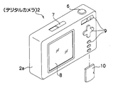
- FIG. 1 is a front perspective view of a digital camera.
- FIG. 2 is a rear perspective view of the digital camera.
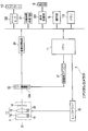
- FIG. 3 is an electrical configuration diagram of the digital camera.
- FIG. 4 is a front view of the imaging surface of the imaging device.
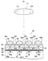
- FIG. 5 is a cross-sectional view of the image sensor.
- FIG. 6 is a block diagram relating to image processing of a digital camera.
- FIG. 7 is an explanatory diagram used for explaining in-focus image generation by the in-focus image generation unit.
- FIG. 8 is an explanatory diagram used for explaining selection of a pixel in the selection unit.
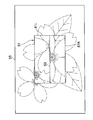
- FIG. 9 is a schematic diagram of an in-focus confirmation image when the focus lens is set at the in-focus position.
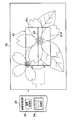
- FIG. 10 is a schematic diagram of an in-focus confirmation image when the focus lens is not set at the in-focus position.
- FIG. 11 is a flowchart showing a flow of photographing processing of the digital camera.
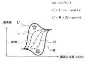
- FIG. 12 is an explanatory diagram illustrating an example of the difference enhancement process in the first embodiment.
- FIG. 13 is an explanatory diagram illustrating an example of the focus confirmation image before and after the difference enhancement processing in the first embodiment.
- FIG. 14 is an explanatory diagram used for explaining a problem of difference enhancement processing when the parallax is large.
- FIG. 15 is an explanatory diagram illustrating a difference enhancement process example when the parallax is small in the second embodiment.
- FIG. 16 is an explanatory diagram illustrating a difference enhancement process example when the parallax is large in the second embodiment.
- FIG. 17 is a flowchart showing the flow of the main part of a difference enhancement processing example in the second embodiment.
- FIG. 18 is an explanatory diagram used for explaining a main part of a difference enhancement processing example according to the second embodiment.
- FIG. 19 is an explanatory diagram showing an example of difference enhancement processing at the time of high contrast in the third embodiment.
- FIG. 20 is an explanatory diagram illustrating an example of difference enhancement processing at the time of low contrast in the third embodiment.
- FIG. 21 is an explanatory diagram used for explaining shading caused by pupil division.
- FIG. 22 is an explanatory diagram used for explaining shading correction information resulting from pupil division.
- FIG. 23 is an explanatory diagram when the difference enhancement process is performed only in the vicinity of the boundary line (split line).
- FIG. 24 is a perspective view of the smartphone.
- FIG. 25 is a configuration diagram of a smartphone.
- a lens barrel 3 including an imaging optical system, a strobe light emitting unit 5 and the like are provided on the front surface of a camera body 2a of a digital camera 2 which is an example of an imaging apparatus of the present invention. It has been.
- a shutter button 6, a power switch 7, and the like are provided on the upper surface of the camera body 2a.
- a focus ring (lens moving mechanism) 3 a used for manual focus (hereinafter simply referred to as “MF”) operation is rotatably attached to the outer peripheral surface of the lens barrel 3.
- a display unit 8 and an operation unit 9 are provided on the back surface of the camera body 2a.
- the display unit 8 functions as an electronic viewfinder in a shooting standby state, and displays a live view image (also referred to as a through image). At the time of image reproduction, the image is reproduced and displayed on the display unit 8 based on the image data recorded on the memory card 10.
- the operation unit 9 is composed of various switches.
- the operation unit 9 in this example includes a mode switch, a cross key, an execution key, and the like.
- the mode switch is operated when switching the operation mode of the digital camera 2.
- the digital camera 2 has a shooting mode for capturing a captured image by capturing a subject, a playback mode for reproducing and displaying the captured image, and the like.
- the shooting mode includes an AF mode for performing autofocus (hereinafter simply referred to as “AF”) and an MF mode for performing MF operation.
- AF AF mode for performing autofocus
- MF mode for performing MF operation.
- the cross key and execution key are used for various operations.
- the cross key and the execution key in this example are input devices for changing instructions such as the position and number of split lines (hereinafter also referred to as “boundary lines”) when a focus confirmation image described later is displayed.
- the cross key and the execution key display a menu screen or a setting screen on the display unit 8, move a cursor displayed in the menu screen or the setting screen, or determine various settings of the digital camera 2. It is operated when doing.
- a card slot into which the memory card 10 is loaded and a loading lid that opens and closes the opening of the card slot are provided.
- the CPU 11 of the digital camera 2 executes various programs and data read from the memory 13 sequentially based on a control signal from the operation unit 9 to control each unit of the digital camera 2 in an integrated manner.
- the RAM area of the memory 13 functions as a work memory for the CPU 11 to execute processing and a temporary storage destination for various data.
- the lens barrel 3 incorporates a photographing lens 17 including a zoom lens 15 and a focus lens 16, a mechanical shutter 18, and the like.
- the zoom lens 15 and the focus lens 16 are driven by the zoom mechanism 19 and the focus mechanism 20, respectively, and are moved back and forth along the optical axis O1 of the photographing lens 17.
- the zoom mechanism 19 and the focus mechanism 20 are configured by gears, motors, and the like.
- the focus mechanism 20 is connected to the focus ring 3a (focus operation unit) through a gear (not shown). For this reason, the focus mechanism 20 moves the focus lens 16 along the direction of the optical axis O1 (hereinafter referred to as “optical axis direction”) as the focus ring 3a is rotated in the MF mode. That is, a focus operation for changing the position (focus position) of the focus lens of the photographing lens 17 is performed by the focus ring 3a.
- the mechanical shutter 18 has a movable part (not shown) that moves between a closed position where the object light is prevented from entering the image sensor 23 and an open position where the object light is allowed to enter.
- the mechanical shutter 18 opens / blocks the optical path from the photographing lens 17 to the image sensor 23 by moving the movable part to each position.
- the mechanical shutter 18 includes a diaphragm for controlling the amount of subject light incident on the image sensor 23.
- the mechanical shutter 18, zoom mechanism 19, and focus mechanism 20 are controlled by the CPU 11 via a lens driver 25.
- a color image sensor 23 (hereinafter simply referred to as “image sensor”) is disposed behind the mechanical shutter 18.
- the image sensor 23 converts the subject light that has passed through the photographing lens 17 and the like into an electrical output signal and outputs it.
- the image sensor 23 may be any type of image sensor such as a CCD (Charge-Coupled Device) -type image sensor or a CMOS (Complementary-Metal-Oxide-Semiconductor) type image sensor.
- the image sensor driver 27 controls driving of the image sensor 23 under the control of the CPU 11.
- the image processing circuit 29 performs various processes such as gradation conversion, white balance correction, and ⁇ correction processing on the output signal (output) from the image sensor 23 to generate captured image data.
- the image processing circuit 29 In the MF mode, the image processing circuit 29 generates split image data for MF operation (hereinafter also referred to as “focus confirmation image”) in addition to the captured image data.
- the captured image data and split image data are temporarily stored in the VRAM area of the memory 13 (a VRAM may be provided separately).
- the VRAM area has a memory area for live view images that stores two continuous field fractions, and sequentially stores captured image data and split image data.
- the compression / decompression processing circuit 31 performs compression processing on the captured image data stored in the VRAM area when the shutter button 6 is pressed.
- the compression / decompression processing circuit 31 performs decompression processing on the compressed image data obtained from the memory card 10 via the media I / F 32.
- the media I / F 32 records and reads captured image data with respect to the memory card 10.
- the display control unit 33 reads captured image data and split image data stored in the VRAM area and sequentially outputs them to the display unit 8 in the shooting mode. Further, the display control unit 33 outputs the captured image data expanded by the compression / decompression processing circuit 31 to the display unit 8 in the reproduction mode.
- ⁇ Configuration of color image sensor> As shown in FIG. 4, on the imaging surface 23a (see FIG. 3) of the image sensor 23, a red (R) R pixel 35, a green (G) G pixel 36, and a blue (B) color. B pixels 37 are arranged in a matrix. Each of the color pixels 35, 36, and 37 is a normal pixel on which a subject image is formed without being divided into pupils, and includes a photoelectric conversion element 39 (see FIG. 5) and three primary colors arranged above the photoelectric conversion element 39. One of the color filters 40 (see FIG. 5) is included. That is, each of the color pixels 35 to 37 can be said to be a non-pupil divided photoelectric conversion element with the color filter 40. Note that “upward” and “upward” indicate directions from the semiconductor substrate 45 to the microlens 49 in FIG. 5 (upward direction in the drawing).
- color filters 40 of R color, G color, and B color are provided, respectively.
- the color filter array (pixel array) of the image sensor 23 has the following features (1), (2), (3), (4), (5), and (6).
- the color filter array includes a non-Bayer array basic array pattern P composed of square array patterns corresponding to 6 ⁇ 6 pixels, and the basic array pattern P is repeatedly arranged in the horizontal direction and the vertical direction.
- RGB color filters 40 are arranged with a predetermined periodicity as described above, R, G, and B signals read from the image sensor 23 are synchronized (interpolated) as compared with a conventionally known random arrangement.
- processing demosaic processing
- processing can be performed according to a repeated pattern.
- the color filter array after the thinning process can be the same as the color filter array before the thinning process, and a common processing circuit is used. be able to.
- the G color filter corresponding to the color that contributes most to obtain the luminance signal corresponds to the horizontal, vertical, and diagonal directions (diagonally upper right and One or more lines are arranged in each line in the direction of diagonally lower left, diagonally lower right, and diagonally upper left.
- the G color filters are arranged in the horizontal, vertical, and diagonal lines of the color filter array in this way, pixel interpolation processing (synchronization processing, etc.) in the high-frequency region is performed regardless of the high-frequency direction. ) Reproduction accuracy can be improved.
- the numbers of R pixels 35, G pixels 36, and B pixels 37 are 8 pixels, 20 pixels, and 8 pixels, respectively. That is, the ratio of the number of pixels of each of the R, G, and B pixels 35 to 37 is 2: 112, and the ratio of the number of pixels of the G pixel 36 is that of each of the R pixel 35 and B pixel 37 of other colors. It becomes larger than the ratio of the number of pixels.
- the ratio between the number of G pixels 36 and the number of R and B pixels 35 and 37 is different, and in particular, the ratio of the number of G pixels 36 that contributes most to obtain a luminance signal is represented by R and B pixels. Since the pixel ratio is larger than the ratio of the number of pixels of 31537, aliasing during pixel interpolation processing (synchronization processing or the like) can be suppressed and high-frequency reproducibility can be improved.
- the color filter array includes R and B color filters 40 corresponding to two or more other colors (in this embodiment, R and B colors) other than the G color in the basic array pattern P. One or more are arranged in each horizontal and vertical line of the array.
- the R color filter 40 and the B color filter 40 are arranged in the horizontal and vertical lines of the color filter array, respectively, the occurrence of color moire (false color) can be reduced.
- an optical low-pass filter for suppressing the generation of false color can be prevented from being arranged in the optical path from the incident surface of the optical system to the imaging surface, or the occurrence of false color can be prevented even when the optical low-pass filter is applied. Therefore, it is possible to apply a low-frequency component for cutting high-frequency components, and not to impair the resolution.
- the color filter array includes a square array corresponding to 2 ⁇ 2 G pixels 36 provided with the G color filter 40. Such a 2 ⁇ 2 G pixel 36 is taken out, the difference absolute value of the pixel value of the G pixel 36 in the horizontal direction, the absolute value of the difference of the pixel value of the G pixel 36 in the vertical direction, and the pixel value of the G pixel 36 in the oblique direction It is possible to determine that there is a correlation in the direction in which the difference absolute value is small among the horizontal direction, the vertical direction, and the diagonal direction.
- this color filter array it is possible to determine a direction having a high correlation among the horizontal direction, the vertical direction, and the diagonal direction using the information of the G pixel 36 having the minimum pixel interval.
- This direction discrimination result can be used for interpolation processing (synchronization processing or the like) for interpolation from surrounding pixels.
- the basic array pattern P is point-symmetric with respect to its center (the centers of the four G color filters 40).
- the four 3 ⁇ 3 sub-arrays in the basic array pattern P are also point-symmetric with respect to the central G color filter 40. Such symmetry makes it possible to reduce or simplify the circuit scale of the subsequent processing circuit.
- phase difference pixel On the partial area (for example, the central area) of the imaging surface 23a, instead of the partial G pixel 36, the first phase difference pixel 36a (indicated by “G1 in a circle” in the figure), the second position A phase difference pixel 36b (indicated by “G2 in a circle” in the figure) is provided.
- the first phase difference pixel 36 a and the second phase difference pixel 36 b are spaced apart from each other by a plurality of vertical columns (second pixel columns) 42 and a plurality of horizontal rows (first pixel columns) 43 in the pixel array of the image sensor 23. They are provided alternately (in the figure, one vertical row 42 and a horizontal line 43 are represented by symbols).
- reference numerals “42” and “43” are respectively attached to the vertical columns where the phase difference pixels are provided and the horizontal rows.
- the “plural vertical columns 42” are provided at a pitch of 3 pixels along the horizontal direction (first direction). Further, the “plurality of horizontal lines 43” are provided along the vertical direction (second direction) at a 4-pixel pitch interval, an 8-pixel pitch interval, a 4-pixel pitch interval, an 8-pixel pitch interval,.
- first phase difference pixels 36a and the second phase difference pixels 36b are alternately arranged along the horizontal direction and the vertical direction, respectively, on the positions where the vertical columns 42 and the horizontal rows 43 intersect.
- the interval between the same type of phase difference pixels is 12 pixel pitch in the vertical direction and 6 in the horizontal direction. This is the pixel pitch.
- FIG. 5 showing a cross section of the horizontal parallel 43, photoelectric conversion elements 39 are formed in a matrix on the surface layer of the semiconductor substrate (sub) 45.
- the semiconductor substrate 45 is provided with various circuits used for driving each pixel and outputting signals.
- a light-transmissive insulating film 46 is provided on the semiconductor substrate 45.
- a light shielding film 47 is provided on the insulating film 46.
- the light shielding film 47 has a normal opening 47a, a first eccentric opening 47b, and a second eccentric opening 47c.
- the first and second eccentric openings 47b and 47c are formed with a smaller opening diameter than the normal opening 47a.
- the normal opening 47a is formed on the photoelectric conversion elements 39 of the RGB pixels 35 to 37.
- the center of the normal opening 47 a is located on the center of the photoelectric conversion element 39.
- the first eccentric opening 47b is formed on the photoelectric conversion element 39a of the first phase difference pixel 36a.
- the center of the first eccentric opening 47b is shifted to the right in the figure with respect to the center of the photoelectric conversion element 39a below the first eccentric opening 47b.
- a substantially left half region (hereinafter simply referred to as a left region) of the photoelectric conversion element 39a of the first phase difference pixel 36a is covered with the light shielding film 47, and conversely a substantially right half region (hereinafter simply referred to as a right region). ) Is exposed.
- the second eccentric opening 47c is formed on the photoelectric conversion element 39b of the second phase difference pixel 36b.
- the center of the second eccentric opening 47c is formed at a position shifted in the right direction in the figure with respect to the center of the photoelectric conversion element 39b below the second eccentric opening 47c.
- a light-transmitting flattening layer 48 having a flat surface is provided on the light shielding film 47.
- color filters 40 of R, G, and B colors are provided at positions corresponding to the pixels 35 to 37 of R, G, and B colors, respectively.
- a G color filter 40 is provided at a position corresponding to the first and second phase difference pixels 36a and 36b.
- a microlens 49 is provided on each color filter 40 and above the photoelectric conversion elements 39, 39a, 39b.
- Various layers such as a light-transmitting flat layer may be provided between the color filter 40 and the microlens 49.
- the subject light 50L incident on the micro lens 49 on the RGB pixels 35 to 37 from the left oblique direction in the drawing is condensed on the right region of the photoelectric conversion element 39 by the micro lens 49.
- the subject light 50 ⁇ / b> R incident on the microlens 49 from the right oblique direction in the drawing is condensed on the left region of the photoelectric conversion element 39 by the microlens 49. Therefore, the RGB pixels 35 to 37 are highly sensitive to both the subject light 50L and the subject light 50R.
- the subject light 50L incident on the microlens 49 on the first phase difference pixel 36a is condensed by the microlens 49 on the right region of the photoelectric conversion element 39a through the first eccentric opening 47b.
- the subject light 50 ⁇ / b> R that has entered the microlens 49 is shielded by the light shielding film 47, and thus is not condensed on the left region of the photoelectric conversion element 39.
- the subject light 50R incident on the microlens 49 on the second phase difference pixel 36b is condensed by the microlens 49 on the left region of the photoelectric conversion element 39b through the second eccentric opening 47c.
- the subject light 50 ⁇ / b> R that has entered the microlens 49 is shielded by the light shielding film 47, and thus is not condensed on the left region of the photoelectric conversion element 39. Therefore, the light shielding film 47 functions as a pupil division unit that performs pupil division.
- the microlens 49 may be eccentric.
- Subject light 50L and 50R are subject light that has passed through the left region 17L and the right region 17R of the photographing lens 17 (the zoom lens 15 and the focus lens 16), respectively.
- the lenses 15 and 16 are shown in an integrated manner, and the sizes of the photographing lens 17 and the image sensor 23 are also different from the actual size.
- the subject light incident on the image sensor 23 is pupil-divided by the light shielding film 47, so that the first phase difference pixel 36a has higher sensitivity to the subject light 50L, and conversely, the second phase difference pixel 36b has the subject light 50R. Sensitivity increases.
- the image sensor 23 of the present example has a plurality of first images in which subject light (subject light 50L, subject light 50R) that has passed through different regions (the left region 17L and the right region 17R) of the photographing lens 17 is divided into pupils.
- One phase difference pixel 36a hereinafter referred to as “first pixel”
- second pixels a plurality of second phase difference pixels 36b
- third pixel a plurality of normal pixels on which the subject image is formed without pupil division 35, 36, and 37
- the image processing circuit 29 includes a normal processing unit 52 and a split image processing unit 54.
- the split image processing unit 54 includes a selection unit 102, an image generation unit 104, and a difference enhancement processing unit 106.
- the normal processing unit 52 performs image processing on the third image 58c that is an output signal (output) of the third pixel group 57c configured by a plurality of third pixels (normal pixels 35, 36, and 37), and The third image 58c (third image) subjected to the image processing is output as a color captured image 55.
- the split image processing unit 54 includes a first image 58a that is an output signal (output) of a first pixel group 57a configured by a plurality of first pixels (first phase difference pixels 36a), and a plurality of second pixels (first pixels).
- a black and white split image 61 (focus confirmation image) is generated based on the second image 58b which is an output signal (output) of the second pixel group 57b composed of the two phase difference pixels 36b).
- the selection unit 102 forms a split image 61 from a first image 58a that is an output signal (output) of the first pixel group 57a and a second image 58b that is an output signal (output) of the second pixel group 57b.
- the display parts (first divided image 61L, second divided image 61R) to be extracted are extracted.
- the selection unit 102 selects the first image 58 a and the second image 58 b output from the first pixel group 57 a and the second pixel group 57 b of the image sensor 23, respectively.
- the selection of which pixel (image pixel) to use for the generation of the split image 61 out of the corresponding pixel 59a of the first image 58a and pixel 59b of the second image 58b is performed.
- one part (for example, the upper half) of the split image 61 is extracted from the first image 58a, and the other part (for example, the lower half) of the split image 61 is extracted from the second image 58b.
- the difference enhancement processing unit 106 performs difference enhancement processing for enhancing the difference in pixel value between the first divided image 61L based on the pixel value of the first pixel 36a and the second divided image 61R based on the pixel value of the second pixel 36b. . Specifically, the difference enhancement processing unit 106 uses the split line 63 as a reference in the split image 61 (focus confirmation image), and first pixels corresponding to each other in a direction perpendicular to the split line 63 with the split line 63 interposed therebetween. The difference in pixel value between the second pixel (59b in FIG. 8) and the second pixel (59b in FIG. 8) is increased.
- the image generation unit 104 includes a display portion (first divided image 61 ⁇ / b> L) of the first image 58 a extracted from the first image 58 a by the selection unit 102, and a second display by the selection unit 102.
- the split image 61 is generated using the display portion (second divided image 61R) of the second image 58b extracted from the image 58b.
- the split image processing unit 54 determines the upper half area of the center area of the subject in the figure on the L (left) viewpoint side based on the luminance component of the output signal (output) from the first pixel group 57a.
- a first black-and-white divided image 61L (display portion of the first image 58a) when viewed from above is generated.
- the split image processing unit 54 is based on the luminance component of the output signal (output) from the second pixel group 57b when the lower half of the center area of the subject is viewed from the R (right) viewpoint side.
- a black and white second divided image 61R (display portion of the second image 58b) is generated.
- a black and white split image 61 including the first divided image 61L and the second divided image 61R is obtained.
- the first divided image 61L and the second divided image 61R are arranged in the split image 61 adjacent to the boundary with a split line 63 (also referred to as a “boundary line”) parallel to the horizontal direction.
- a split line 63 also referred to as a “boundary line” parallel to the horizontal direction.
- the captured image 55 (third image 58c after image processing) and the split image 61 are temporarily stored in the VRAM area of the memory 13.
- the display control unit 33 reads the captured image 55 and the split image 61 from the memory 13, combines the split image 61 with the captured image 55, and outputs the composite image to the display unit 8. Thereby, the user can see the live view image in which the black and white split image 61 is displayed in the display area of the full-color captured image 55.
- the first divided image 61L, which is the display portion of the first image 58a, and the second divided image 61R, which is the display portion of the second image 58b, are displayed in the horizontal direction [horizontal direction ( Shift to the first direction)].
- the shift amount between the first divided image 61L and the second split image 61R at this time corresponds to the focus shift amount of the focus lens 16. That is, the horizontal direction in the figure is the phase difference direction corresponding to the shift direction of the image of each subject light imaged on the imaging surface 23a by the photographing lens 17.
- the first divided image 61L and the second divided image 61R have a deviation amount of zero (including almost zero) when the focus lens 16 is in focus.
- the shift amount between the first divided image 61L and the second divided image 61R increases as the focus lens 16 defocuses. Accordingly, the user can perform focus adjustment while confirming the live view image.
- a subject that is not in focus is indicated by a two-dot chain line.
- the split image 61 (focus confirmation) is displayed in the display area of the captured image 55, which is an image after image processing of the third image 58c (normal image) output from the third pixel group 57c.
- the image is displayed.
- only the split image 61 may be displayed on the display unit 8. That is, all the pixels of the image sensor 23 are phase difference pixels (first phase difference pixel and second phase difference pixel), or phase difference pixels (first phase difference pixels) at a certain ratio in the entire area of the image sensor 23. Pixels and second phase difference pixels) may be arranged, and only the split image 61 may be displayed on the display unit 8.
- the digital camera 2 is provided with an AF detection circuit for autofocus and the like.
- the AF detection circuit analyzes the image formed by the output signal of the first pixel 36a and the image formed by the output signal of the second pixel 36b, and determines the shift direction of both images and the shift amount between the two images. By detecting this, the focus adjustment amount (also referred to as defocus amount) of the photographing lens 17 is obtained. Based on this focus adjustment amount, the CPU 11 controls the lens driver 25 and drives the focus lens 16 by the focus mechanism 20 to perform focus adjustment. Since the phase difference type AF processing is known, a specific description is omitted here.
- the digital camera 2 is provided with an AE detection circuit and the like.
- the CPU 11 executes the AE process by driving the mechanical shutter 18 via the lens driver 25 based on the detection result of the AE detection circuit.
- step S2 the operation of the digital camera 2 configured as described above will be described with reference to FIG.
- step S3 the operation of the digital camera 2 when the AF mode is set.
- step S2 When the MF mode (step S2) is set, output signals from the third pixels 35, 36, and 37 (normal pixels) of the image sensor 23 are input to the normal processing unit 52 of the image processing circuit 29.
- the normal processing unit 52 performs image processing on the third image 58c, which is an output signal from the third pixels 35 to 37, and stores it as a full-color captured image 55 in the VRAM area of the memory 13 (step S4).
- the selection unit 102 extracts the first divided image 61L and the second divided image 61R used for the in-focus confirmation image from the first image 58a and the second image 58b, respectively.
- the difference enhancement processing unit 106 performs difference enhancement processing for enhancing the difference in pixel values between the first divided image 61L and the second divided image 61R. Specifically, the difference enhancement processing unit 106 uses the split line 63 of the split image 61 (focus confirmation image) as a reference, and the first pixel 36 a and the second pixel 36 b corresponding in a direction orthogonal to the split line 63. To increase the difference in pixel values.
- the image generation unit 104 generates a split image 61 including the black and white first divided image 61L and the black and white second divided image 61R (step S5). Note that the difference enhancement process between the first divided image 61L and the second divided image 61R is performed in step S5.
- the generated split image 61 is stored in the VRAM area of the memory 13.
- the display control unit 33 reads the captured image 55 and the split image 61 from the memory 13, synthesizes the split image 61 in the display area of the captured image 55, and then outputs the composite image to the display unit 8. Accordingly, as shown in FIG. 10, a live view image including a black and white split image 61 is displayed on the display unit 8 in the color captured image 55 (step S6).
- the user rotates the focus ring 3a to move the focus lens 16 Move along the optical axis direction.
- the focus lens 16 approaches the in-focus position where the subject is focused, the amount of deviation between the first image 66L and the second image 66R gradually decreases. Accordingly, the user can perform focus adjustment while confirming the live view image.
- the focus lens 16 When the focus lens 16 is set at the in-focus position, as shown in FIG. 9, the deviation amount between the first image 66L and the second image 66R becomes zero. Thereby, the focus lens 16 is focused on the subject, and the focus adjustment is completed. Thereafter, the above process is repeatedly executed until the shutter button 6 is pressed.
- step S7 It is determined whether or not a shooting instruction has been input by pressing the shutter button 6 (Yes in step S7).
- the normal processing unit 52 performs one frame worth.
- the captured image 55 is generated and temporarily stored in the VRAM area of the memory 13.
- the captured image 55 is compressed by the compression / decompression processing circuit 31, and then recorded on the memory card 10 via the media I / F 32 (step S8). Thereafter, it is determined whether or not the photographing is continued due to the end of the MF mode (step S9), and the above-described processing is repeatedly executed until the MF mode is ended.
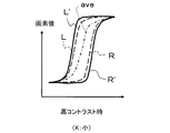
- the difference enhancement processing unit (106 in FIG. 6) is provided for each pair of pixels (PR in FIG. 8) that face each other across the split line (63 in FIGS. 9 and 10).
- difference enhancement processing is performed to increase the difference (
- L is the pixel value of the first pixel 36a before the difference enhancement process
- R is the pixel value of the second pixel 36b before the difference enhancement process
- ave is the pixel value L of the first pixel 36a before the difference enhancement process.
- the average value ((L + R) / 2) with the pixel value R of the second pixel 36b
- L ′ is the pixel value of the first pixel 36a after the difference enhancement process
- R ′ is the pixel of the second pixel 36b after the difference enhancement process Value.
- the difference enhancement processing unit 106 of this example increases the difference (
- difference enhancement is performed as shown in the following equation.
- the difference enhancement processing unit 106 of this example decreases the difference enhancement coefficient K as the difference between the pixel value L of the first pixel 36a and the pixel value R of the second pixel 36b increases.
- each of the first divided image 61L and the second divided image 61R constituting the split images 61a and 61b has a constant pixel value in a direction y (vertical direction) orthogonal to the split line 63.
- the first divided image 61L and the second image 61L are compared.
- the difference between the pixel values of the first divided image 61L and the second divided image 61R is increased and emphasized.
- the first divided image 61L and the second divided image 61R It can be seen that the parallax d (phase difference) in the x-direction (left-right direction) is easily visible.
- an average value ave between the pixel value L of the pixel (first pixel) of the first divided image 61L and the pixel value R of the pixel (second pixel) of the second divided image 61R that are opposed to each other across the split line 63 is calculated. Based on the average value ave, the difference between the pixel value L of the pixel (first pixel) of the first divided image 61L and the average value ave, and the pixel value of the pixel (second pixel) of the second divided image 61R Since the difference between R and the average value ave is increased, the image structure in the first divided image 61L and the second divided image 61R is not substantially changed even if the difference in pixel value is enhanced.
- the shift amount in the focus confirmation image (split image) can be easily visually confirmed.
- the image processing circuit (29 in FIG. 6) is as described above, and the difference enhancement processing unit (106 in FIG. 6) constituting the image processing circuit 29 performs split line 63 in the vertical direction y as the difference enhancement processing.
- LR ⁇ between the pixel value L of the first pixel 59a and the pixel value R of the second pixel 59b is increased for the corresponding first pixel 59a and second pixel 59b.
- the difference emphasis processing unit 106 of the present embodiment will be described with respect to differences from the first embodiment.
- the CPU 11 (calculation unit) of the present embodiment has a pixel (first pixel 59a) of the first divided image 61L that is a display portion of the first image 58a and a pixel of the second divided image 61R that is a display portion of the second image 58b.
- the parallax with the (second pixel 59b) is calculated.
- the parallax indicates the blur amount of the third image 58c (normal image), and the left-right direction x (the horizontal direction along the split line 63) between the first divided image 61L and the second divided image 61R in the split image 61. This is equivalent to the amount of deviation.
- the difference enhancement processing unit 106 of the image processing circuit 29 determines the magnitude of the parallax (blur amount) between the first divided image 61L and the second divided image 61R in the split image 61 based on the parallax calculated by the CPU 11.
- LR ⁇ when the parallax is determined to be large is larger than the increase amount of the pixel value difference
- 14A is a split image 61 before the difference enhancement process, and the parallax d (the amount of shift in the horizontal direction x along the split line 63 between the first divided image 61L and the second divided image 61R). Shows a large case.
- the part with the parallax d becomes a pure white and black part with no grayscale, and the user can confirm the size of the parallax, but it is possible to see what kind of subject the part with the parallax is. It becomes difficult to do.
- the part where the parallax is sufficient is easy to visually recognize the parallax without performing the difference emphasis, but when the difference emphasis is performed, the gradation of gradation is lost and it becomes difficult to visually recognize what the subject is. .
- the difference enhancement processing unit 106 determines the magnitude of the parallax d between the first divided image 61L and the second divided image 61R in the split image 61 (focus confirmation image), and performs a difference according to the parallax d.
- LR ⁇ when the parallax d is determined to be large is changed to the pixel value difference
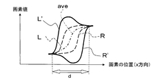
- FIG. 15 is a characteristic diagram showing parallax enhancement when the parallax d is small
- FIG. 16 is a characteristic diagram showing parallax enhancement when the parallax d is large.
- the horizontal axis indicates the pixel position in the horizontal direction (left-right direction x) along the split line 63
- the vertical axis indicates the pixel value.
- the following method can be given as a specific example in which the magnitude of parallax is easily determined and the difference enhancement is appropriately performed.
- LR ⁇ of the pixel value in the vertical direction y is larger than the threshold value Tp is detected in the split image 61, and the horizontal direction x (direction along the split line) of the detected region is detected.
- the width is detected, and the difference enhancement coefficient K is switched according to the detection result. For example, the difference enhancement coefficient K is decreased as the detected width is increased.
- threshold value Tp ⁇ 0 and Tp 0
- width parallax d.
- the width obtained as Tp> 0 (the value corresponding to the parallax d, although not the same as the parallax d) is also referred to as “parallax” in this specification.
- LR ⁇ between the pixel value of the first pixel 59a and the pixel value of the second pixel 59b corresponding to the first pixel 59a is larger than a threshold value.
- the difference enhancement coefficient K is switched according to the detection result. For example, the difference enhancement coefficient K is decreased as the number of pixels in which the difference
- FIG. 17 is a flowchart showing the flow of the main part of the difference enhancement processing example in the present embodiment. This process is executed by the difference enhancement processing unit 106 according to a program.
- the difference enhancement coefficient K is switched by the second method (detecting the number of pixels per unit length).
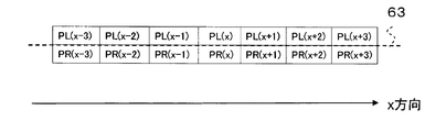
- the difference enhancement processing unit 106 includes neighboring pixel columns in the left-right direction x including the target pixel PL (x) (in this example, PL (x-3), PL (x-2), PL (X ⁇ 1), PL (x), PL (x + 1), PL (x + 2), and PL (x + 3) in a range of pixels), a pixel having a pixel value difference
- the difference enhancement processing unit 106 compares the pixel values within the range of the neighboring pixel row in the left-right direction x including the target pixel PL (x) (a total of seven pixels from PL (x ⁇ 3) to PL (x + 3)). It is determined whether or not there are five or more pixels of
- the difference enhancement processing unit 106 of this example performs a pixel value difference
- the difference enhancement processing unit 106 cannot detect the presence of five or more consecutive pixels in which
- ” (“40”, “20”) and the threshold value of the number of pixels (5 pixels) are examples, and are not limited to these threshold values.
- the digital camera 2 including the difference enhancement processing unit 106 of the present embodiment the pixels of the first divided image 61L that correspond to each other with respect to the split line 63 (boundary line) in the split image 61 (focus confirmation image). And the pixel of the second divided image 61R is determined, and the increase amount of the pixel value difference
- the image processing circuit (29 in FIG. 6) and the difference enhancement processing unit 106 that constitutes the image processing circuit 29 are as described above.
- splitting is performed in the vertical direction y (direction orthogonal to the split line 63).
- the first pixel 59a and the second pixel 59b corresponding to each other across the line 63 increase the difference
- LR ⁇ between the pixel value L of the first pixel 59a and the pixel value R of the second pixel 59b.
- the difference enhancement processing unit 106 of this embodiment determines the magnitude of the difference
- FIG. 19 is a characteristic diagram showing difference emphasis when the difference
- FIG. 20 is a characteristic diagram when the difference
- the difference enhancement processing unit 106 of the present embodiment weakens difference enhancement at the time of high contrast shown in FIG. 19 and strengthens difference enhancement at the time of low contrast shown in FIG.
- the difference enhancement processing unit 106 switches the magnitude of the difference enhancement coefficient K based on the difference
- the value of the difference enhancement coefficient K may be obtained by a function using the pixel value difference
- a function is suitable in which the larger the pixel value difference, the smaller the K value and the smaller the K value change amount.
- K 5 ⁇ exp (0.01 ⁇ ( ⁇
- x is the position in the left-right direction (that is, the direction along the split line 63) in the split image 61.
- LR ⁇ between the first pixel 59a and the second pixel 59b facing each other across the split line 63 is high.
- an excessive difference at the time of high contrast can be obtained by setting the difference emphasis coefficient K to be smaller than that at the time of low contrast where the difference
- Sufficient difference enhancement can be performed at low contrast while avoiding enhancement.
- the image processing circuit (29 in FIG. 6) and the difference enhancement processing unit 106 that constitutes the image processing circuit 29 are as described above.
- the difference enhancement processing unit 106 of the present embodiment is the same as that of the first embodiment. Explains the different points.
- the difference enhancement processing unit 106 performs difference enhancement processing using a shading correction coefficient for correcting shading due to pupil division of the image sensor 23, thereby enhancing shading components due to pupil division. To avoid.
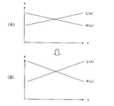
- 21A shows a shading characteristic L (x) generated in the first divided image 61L due to pupil division of the image sensor 23 and a shading characteristic R (x) generated in the second divided image 61R.
- x indicates a position in the left-right direction x.
- the characteristics L (x) and R (x) are obtained by imaging with uniform luminance.
- different shading occurs between the first divided image 61L and the second divided image 61R, and when difference enhancement is performed on an image including such a shading component, FIG.
- the shading component is emphasized.
- the difference emphasis processing unit 106 of the present embodiment uses the shading correction coefficient so that the shading component is not included in the difference emphasis component (the increase of
- the shading correction coefficient is calculated for the shading characteristics L (x) and R (x) shown in part (A) of FIG. ⁇ (x).
- x indicates a position in the left-right direction x.
- the difference enhancement processing unit 106 calculates the shading correction coefficient for the first divided image 61L by ⁇ (x), the shading correction coefficient for the second divided image 61R by ⁇ (x), and an average value obtained by calculating the shading correction coefficient.
- Is ave (x) ( ⁇ (x) ⁇ L (x) + ⁇ (x) ⁇ R (x)) / 2
- the difference enhancement coefficient is K (x) (where K (x)> 0)
- the difference enhancement processing is performed on the entire first divided image 61L and the second divided image 61R in the split image 61 is taken as an example.
- the difference enhancement processing may be performed only on the region 67 in the vicinity of the split line 63 (boundary line) in the first divided image 61L and the second divided image 61R. Good.
- the “neighboring region” of the split line 63 is, for example, a dividing boundary line with respect to the total number of pixels in the dividing direction of the split image 61 (focus confirmation image) (y direction orthogonal to the split line 63). This is an area having the number of pixels within ⁇ 10% from (split line 63).
- split line 63 In the first to third embodiments described above, the case where there is one split line 63 has been described as an example. However, a plurality of split lines 63 may be provided in the split image 61, and a plurality of such split lines 63 may be provided. Difference emphasis processing may be performed only on the vicinity of each of the split lines 63.
- the split lines 63 may be provided in a lattice shape in the split image 61, and the difference emphasis processing may be performed only on a region in the vicinity of such a lattice-like split line 63.
- the pixel array (color filter array) of the image sensor 23 of each of the above embodiments is configured by a basic array pattern P corresponding to 6 ⁇ 6 pixels repeatedly arranged in the horizontal and vertical directions, but N ⁇ N pixels ( N may be a basic array pattern of array patterns corresponding to 3 or more.
- the filter color is not limited to the three primary colors RGB.
- a color filter array of four color filters of three primary colors of RGB + other colors for example, emerald (E)
- E emerald
- a color filter array of C (cyan), M (magenta), and Y (yellow) color filters which are complementary colors of the primary colors RGB may be used.
- the pixel array (color filter array) of the image sensor 23 may be a Bayer array.
- a plurality of first phase difference pixels (first pixels) and a plurality of second phase difference pixels (second pixels) are arranged in a part of a pixel array composed of a Bayer array.
- the pixel array (color filter array) of the image sensor 23 may be a pixel array composed of an array of two surfaces in which pixels of the same color are shifted.
- the image sensor 23 of the present example includes a plurality of first phase difference pixels (first pixels) and a plurality of second phase difference pixels (first pixels) in a part of a pixel array composed of two-sided arrays in which the same color pixels are shifted. 2 pixels), and the first phase difference pixel and the second phase difference pixel of the pair pixel are arranged adjacent to each other.
- a digital camera has been described as an example of the imaging apparatus of the present invention.
- the present invention is also applied to a mobile phone or a smartphone having a camera function, a PDA (Personal Digital Assistants), a portable game machine. Can be applied.
- a smartphone will be described as an example, and will be described in detail with reference to the drawings.
- FIG. 24 shows the appearance of the smartphone 500.
- a smartphone 500 illustrated in FIG. 24 includes a flat housing 502, and a display input unit in which a display panel 521 and an operation panel 522 (touch panel) as an input unit are integrated on one surface of the housing 502. 520 (also referred to as a “touch panel display unit”).
- the housing 502 includes a speaker 531, a microphone 532, an operation unit 540, and a camera unit 541.
- the configuration of the housing 502 is not limited to this, and for example, a configuration in which the display unit and the input unit are independent may be employed, or a configuration having a folding structure or a slide mechanism may be employed.
- FIG. 25 is a block diagram showing a configuration of the smartphone 500 shown in FIG.
- the main components of the smartphone include a wireless communication unit 510, a display input unit 520, a call unit 530, an operation unit 540, a camera unit 541, a storage unit 550, and an external input / output unit. 560, a GPS (Global Positioning System) receiving unit 570, a motion sensor unit 580, a power supply unit 590, and a main control unit 501.
- a wireless communication function for performing mobile wireless communication via the base station device BS and the mobile communication network NW is provided as a main function of the smartphone 500.
- the wireless communication unit 510 performs wireless communication with the base station apparatus BS accommodated in the mobile communication network NW according to an instruction from the main control unit 501. Using this wireless communication, transmission and reception of various file data such as audio data and image data, e-mail data, and reception of Web data and streaming data are performed.
- the display input unit 520 displays images (still images and moving images), character information, and the like visually by transmitting information to the user under the control of the main control unit 501, and detects user operations on the displayed information.
- a so-called touch panel which includes a display panel 521 and an operation panel 522.
- the display panel 521 is preferably a 3D display panel.
- the display panel 521 uses an LCD (Liquid Crystal Display), an OELD (Organic Electro-Luminescence Display), or the like as a display device.
- the operation panel 522 is a device that is placed so that an image displayed on the display surface of the display panel 521 is visible and detects one or a plurality of coordinates operated by a user's finger or stylus. When this device is operated by a user's finger or stylus, a detection signal generated due to the operation is output to the main control unit 501. Next, the main control unit 501 detects an operation position (coordinates) on the display panel 521 based on the received detection signal.
- the display panel 521 and the operation panel 522 of the smartphone 500 integrally form the display input unit 520, but the operation panel 522 is disposed so as to completely cover the display panel 521. ing.
- the operation panel 522 may have a function of detecting a user operation even in an area outside the display panel 521.
- the operation panel 522 includes a detection area (hereinafter referred to as a display area) for an overlapping portion that overlaps the display panel 521 and a detection area (hereinafter, a non-display area) for an outer edge portion that does not overlap the other display panel 521. May be included).
- the operation panel 522 may include two sensitive regions of the outer edge portion and the other inner portion. Further, the width of the outer edge portion is appropriately designed according to the size of the housing 502 and the like.
- examples of the position detection method employed in the operation panel 522 include a matrix switch method, a resistance film method, a surface acoustic wave method, an infrared method, an electromagnetic induction method, and a capacitance method. You can also
- the call unit 530 includes a speaker 531 and a microphone 532, and converts a user's voice input through the microphone 532 into voice data that can be processed by the main control unit 501, and outputs the voice data to the main control unit 501, or a wireless communication unit 510 or the audio data received by the external input / output unit 560 is decoded and output from the speaker 531.
- the speaker 531 and the microphone 532 are mounted on the same surface as the surface on which the display input unit 520 is provided.
- a microphone 532 can be mounted on the side surface of the housing 502.
- the operation unit 540 is a hardware key using a key switch or the like, and receives an instruction from the user.
- the operation unit 540 is mounted on the lower and lower side of the display unit of the housing 502 of the smartphone 500, and turns on when pressed with a finger or the like, and restores a spring or the like when the finger is released. It is a push button type switch that is turned off by force.
- the storage unit 550 includes control software and control data for the main control unit 501, application software including an image processing program for generating a left-eye image and a right-eye image according to the present invention, and a first used for generating a stereoscopic image. And the second digital filter group, the parallax map, the address data that associates the name and telephone number of the communication partner, the transmitted / received e-mail data, the web data downloaded by web browsing, and the downloaded content data, It also temporarily stores streaming data and the like.
- the storage unit 550 includes an internal storage unit 551 with a built-in smartphone and an external storage unit 552 having a removable external memory slot.
- Each of the internal storage unit 551 and the external storage unit 552 constituting the storage unit 550 includes a flash memory type (flash memory type), a hard disk type (hard disk type), a multimedia card micro type (multimedia card micro type), It is realized using a storage medium such as a card type memory (for example, Micro SD (registered trademark) memory), RAM (Random Access Memory), ROM (Read Only Memory), or the like.
- flash memory type flash memory type
- hard disk type hard disk type
- multimedia card micro type multimedia card micro type
- a storage medium such as a card type memory (for example, Micro SD (registered trademark) memory), RAM (Random Access Memory), ROM (Read Only Memory), or the like.
- the external input / output unit 560 serves as an interface with all external devices connected to the smartphone 500, and communicates with other external devices (for example, universal serial bus (USB), IEEE1394, etc.) or a network.
- external devices for example, universal serial bus (USB), IEEE1394, etc.
- a network for example, Internet, wireless LAN, Bluetooth (registered trademark), RFID (Radio Frequency Identification), infrared communication (IrDA) (registered trademark), UWB (Ultra Wideband) (registered trademark), ZigBee (Registered trademark) etc.
- Examples of the external device connected to the smartphone 500 include a memory card connected via a wired / wireless headset, wired / wireless external charger, wired / wireless data port, card socket, and SIM (Subscriber).
- Identity Module Card / UIM User Identity Module Card
- external audio / video equipment connected via audio / video I / O (Input / Output) terminal
- external audio / video equipment connected wirelessly, yes / no
- the external input / output unit may transmit data received from such an external device to each component inside the smartphone 500, or may allow data inside the smartphone 500 to be transmitted to the external device. it can.
- the GPS receiving unit 570 receives GPS signals transmitted from the GPS satellites ST1 to STn in accordance with instructions from the main control unit 501, performs positioning calculation processing based on the received plurality of GPS signals, A position consisting of longitude and altitude is detected.
- the GPS reception unit 570 can acquire position information from the wireless communication unit 510 or the external input / output unit 560 (for example, a wireless LAN), the GPS reception unit 570 can also detect the position using the position information.
- the motion sensor unit 580 includes a triaxial acceleration sensor, for example, and detects the physical movement of the smartphone 500 in accordance with an instruction from the main control unit 501. By detecting the physical movement of the smartphone 500, the moving direction and acceleration of the smartphone 500 are detected. This detection result is output to the main control unit 501.
- the power supply unit 590 supplies power stored in a battery (not shown) to each unit of the smartphone 500 in accordance with an instruction from the main control unit 501.
- the main control unit 501 includes a microprocessor, operates according to a control program and control data stored in the storage unit 550, and controls each unit of the smartphone 500 in an integrated manner. Further, the main control unit 501 includes a mobile communication control function for controlling each unit of the communication system and an application processing function in order to perform voice communication and data communication through the wireless communication unit 510.
- the application processing function is realized by the main control unit 501 operating in accordance with application software stored in the storage unit 550.
- Examples of the application processing function include an infrared communication function for controlling the external input / output unit 560 to perform data communication with the opposite device, an e-mail function for sending and receiving e-mails, a web browsing function for browsing web pages, and the present invention. And a function for generating a 3D image from the 2D image according to the above.
- the main control unit 501 has an image processing function such as displaying video on the display input unit 520 based on image data (still image data or moving image data) such as received data or downloaded streaming data.
- the image processing function is a function in which the main control unit 501 decodes the image data, performs image processing on the decoding result, and displays an image on the display input unit 520.
- the main control unit 501 executes display control for the display panel 521 and operation detection control for detecting a user operation through the operation unit 540 and the operation panel 522.
- the main control unit 501 By executing the display control, the main control unit 501 displays an icon for starting application software, a software key such as a scroll bar, or displays a window for creating an e-mail.
- a software key such as a scroll bar
- the scroll bar refers to a software key for accepting an instruction to move the display portion of a large image that does not fit in the display area of the display panel 521.
- the main control unit 501 detects a user operation through the operation unit 540, or accepts an operation on the icon or an input of a character string in the input field of the window through the operation panel 522. Or a display image scroll request through a scroll bar.
- the main control unit 501 causes the operation position with respect to the operation panel 522 to overlap with the display panel 521 (display area) or other outer edge part (non-display area) that does not overlap with the display panel 521.
- a touch panel control function for controlling the sensitive area of the operation panel 522 and the display position of the software key.
- the main control unit 501 can also detect a gesture operation on the operation panel 522 and execute a preset function according to the detected gesture operation.
- Gesture operation is not a conventional simple touch operation, but an operation that draws a trajectory with a finger or the like, designates a plurality of positions at the same time, or combines these to draw a trajectory for at least one of a plurality of positions. means.
- a camera unit (imaging device) 541 is a digital camera that performs electronic photography using an imaging device such as a CMOS (Complementary Metal Oxide Semiconductor) or a CCD (Charge-Coupled Device), and is basically the same as the digital camera of each of the above embodiments. It is the same configuration.
- CMOS Complementary Metal Oxide Semiconductor
- CCD Charge-Coupled Device
- the camera unit 541 converts image data obtained by imaging into compressed image data such as JPEG (Joint Photographic coding Experts Group) under the control of the main control unit 501, and records the data in the storage unit 550 or externally
- the data can be output through the input / output unit 560 and the wireless communication unit 510.
- the camera unit 541 is mounted on the same surface as the display input unit 520, but the mounting position of the camera unit 541 is not limited to this, and the camera unit 541 may be mounted on the back surface of the display input unit 520.
- a plurality of camera units 541 may be mounted. Note that when a plurality of camera units 541 are mounted, the camera unit 541 used for shooting may be switched to shoot alone, or a plurality of camera units 541 may be used for shooting simultaneously. it can.
- the camera unit 541 can be used for various functions of the smartphone 500.
- an image acquired by the camera unit 541 can be displayed on the display panel 521, or the image of the camera unit 541 can be used as one of operation inputs of the operation panel 522.
- the GPS receiving unit 570 detects the position, the position can also be detected with reference to an image from the camera unit 541.
- the optical axis direction of the camera unit 541 of the smartphone 500 can be determined without using the triaxial acceleration sensor or in combination with the triaxial acceleration sensor, The current usage environment can also be determined.
- the image from the camera unit 541 can be used in the application software.
- the position information acquired by the GPS receiver 570 to the image data of the still image or the moving image, the voice information acquired by the microphone 532 (the text information may be converted into voice information by the main control unit or the like), Posture information and the like acquired by the motion sensor unit 580 can be added and recorded in the storage unit 550 or output through the external input / output unit 560 or the wireless communication unit 510.
- the smartphone 500 shown in FIGS. 24 and 25 has the same function as the digital camera 2 described above.
- the main control unit 501 in FIG. 25 has the function of the image processing circuit 29 shown in FIG. 6 or FIG.
- the display input unit 520 (touch panel type display unit) constitutes the “display unit”, “position input unit”, and “number input unit” in the present invention.
- the smartphone 500 of this example receives a drag operation for dragging the split line 63 shown in FIG.
- the display input unit 520 performs a drag operation to drag the split line 63 (boundary line) while the split image 61 (focus confirmation image) is displayed on the display input unit 520
- the main control unit 501 performs dragging.
- the position of the split line 63 in the split image 61 is changed according to the operation.
Landscapes
- Engineering & Computer Science (AREA)
- Multimedia (AREA)
- Signal Processing (AREA)
- Physics & Mathematics (AREA)
- General Physics & Mathematics (AREA)
- Optics & Photonics (AREA)
- Human Computer Interaction (AREA)
- Spectroscopy & Molecular Physics (AREA)
- Studio Devices (AREA)
- Automatic Focus Adjustment (AREA)
- Focusing (AREA)
- Indication In Cameras, And Counting Of Exposures (AREA)
- Image Processing (AREA)
Description
本発明は、マニュアルフォーカス用の合焦確認画像を表示する撮像装置及び合焦確認表示方法に関する。
デジタルカメラとして、位相差検出方式やコントラスト検出方式を用いたオートフォーカスの他に、使用者が手動でフォーカス調整を行うことができる、いわゆるマニュアルフォーカスモードを備えるものがよく知られている。
マニュアルフォーカスモードを有するデジタルカメラとしては、撮影した被写体を確認しながらフォーカス調整ができるようにレフレックスミラーを設けて、目視による位相差を表示するスプリットマイクロプリズムスクリーンを用いた方法や、目視によるコントラストの確認を行う方法を採用しているものが良く知られている。
ところで、近年普及しているレフレックスミラーを省略したデジタルカメラでは、レフレックスミラーがないため位相差を表示しながら被写体像を確認する方法がなく、コントラスト検出方式に頼らざるを得なかった。しかし、この場合には、LCD等の表示装置の解像度以上のコントラスト表示ができず、一部拡大するなどして表示する方法を採らざるを得なかった。
そこで、近年では、マニュアルフォーカスモード時に操作者が被写体に対してピントを合わせる作業を容易にするために、スプリットイメージ(本明細書では「合焦確認画像」ともいう)をライブビュー画像内に表示している。ここで、スプリットイメージは、瞳分割方式の撮像で得られた二つの被写体像(位相差画像)を合成したものであり、被写体像の位相差を表す。つまり、一方の被写体像の上半分と他方の被写体像の下半分とを上下に隣接して配置したスプリットイメージを表示する。ピントがずれた状態だと上下に隣接した二つの被写体像が左右にずれて表示され、ピントが合った状態だと上下に隣接した二つの被写体像の左右のずれがなくなる。操作者は、スプリットイメージ内の二つの被写体像の左右のずれがなくなるように、フォーカスリングを操作してピントを合わせる。
特許文献1に記載のデジタルカメラでは、絞りを光軸と垂直方向に移動させることで二つの測距位置でそれぞれ被写体画像の撮影を行い、これら2つの被写体画像を用いてスプリットイメージをライブビュー画像内に表示している。
特許文献2に記載のデジタルカメラでは、被写体像の像面と撮像素子の受光面との間の距離に相当する値をずれ量として求め、このずれ量に応じて左右相反する方向にずらしたスプリットイメージをライブビュー画像内に表示している。
特許文献3及び4に記載のデジタルカメラは、撮影用の通常画素と、瞳分割された被写体光を受光する焦点検出用の2種類の位相差画素とが撮像面上に複数配列されてなる撮像素子を備えている。このデジタルカメラでは、通常画素からの出力信号に基づき撮像画像を生成してライブビュー画像表示を行うとともに、2種類の位相差画素のそれぞれからの出力に基づきスプリットイメージを生成してライブビュー画像内に表示している。
しかしながら、特許文献1記載のデジタルカメラでは、絞りを移動させる機械的な構成が必要になるので、この構成を収納するスペースの確保、及び部品点数の増加などの問題が生じる。また、特許文献2記載のデジタルカメラでは、被写体光を瞳分割して撮像する構成を有さないので、正確で破綻のないスプリットイメージ(合焦確認画像)の実現が困難である。
特許文献3及び4記載のデジタルカメラでは、2種類の位相差画素を用いてスプリットイメージを生成しているが、僅かにピントが合っていない状態では、スプリットイメージとして上下に表示される二つの被写体像間のずれ量が小さくなるため、スプリットイメージを視認することが容易でなくなり、ユーザがマニュアルのフォーカス操作で十分にピントを合わせることが難しいという課題があった。
二つの被写体像間の視差を強調する視差強調技術も考案されているが、このような視差強調技術では処理負荷が大きく、ライブビュー表示中に視差強調を行うことが困難であった。例えば二つの被写体像間でマッチングを取るマッチング処理の処理負荷が大きい。
本発明の目的は、僅かにピントが合っていない状態でも合焦確認用の画像を見易くすることができる撮像装置及び合焦確認表示方法を提供することにある。
上記の目的を達成するために、本発明は、撮影レンズにおける第1及び第2の領域を通過した被写体光が瞳分割されてそれぞれ入射される第1及び第2の画素群を有する撮像素子から出力された画像信号に基づいて第1の表示用画像を生成し、かつ第1画素群及び第2の画素群からそれぞれ出力された第1画像及び第2画像に基づいて合焦確認に使用する第2の表示用画像を生成する画像生成部と、第1画像の第1画素と第1画素に対応する第2画像の第2画素との画素値の差分を大きくする差分強調処理を行う差分強調処理部と、表示部と、第1の表示用画像を表示部に表示させ、第1の表示用画像の表示領域内に、差分強調処理部によって差分強調処理が行われた第2の表示用画像を表示する表示制御部と、を備えた撮像装置を提供する。
これによれば、第2の表示用画像(合焦確認画像)を構成する第1画像と第2画像とで境界線を挟んで画素値の差分が強調されるので、視差が小さい場合でも第2の表示用画像(合焦確認画像)を見易くすることができ、かつ、視差強調を行う場合と比較して、ライブビュー表示中でも低負荷で強調された第2の表示用画像(合焦確認画像)を表示することができる。
一実施形態では、撮像素子は、被写体光が瞳分割されずに入射される第3の画素群をさらに有し、第1の表示用画像は第3の画素群から出力された第3画像(通常画像)に基づいて生成される。
一実施形態では、差分強調処理部は、第1画素の画素値と第1画素に対応する第2画素の画素値との平均値を算出し、平均値を基準に、第1画素の画素値と平均値との差分、及び第1画素に対応する第2画素の画素値と平均値との差分をそれぞれ大きくする。これによれば、第1画像と第2画像との位相差を視認し易くすることができるだけでなく、第1画像及び第2画像の像構造をほぼ変えないようにすることができる。
一実施形態では、第1画像の第1画素と第1画素に対応する第2画像の第2画素との視差を算出する算出部を備え、差分強調処理部は、算出部によって算出された視差に基づいて、第1画像と第2画像との視差の大小を判定し、視差の大小の判定結果に基づいて差分強調処理を行う。また、一実施形態では、差分強調処理部は、視差の大小を判定した結果、視差が大きいと判定した場合には、視差が小さいと判定した場合よりも、画素値の差分の増加量を小さくする。また、一実施形態では、差分強調処理部は、第1画素の画素値と第1画素に対応する第2画素の画素値との差分が閾値よりも大きい画素が何画素連続して存在するかを判定し、連続している画素の数が多いほど画素値の差分の増加量を小さくする。これによれば、十分に視差がついた箇所に対し過度な差分強調を行わないようになり、第2の表示用画像(合焦確認用画像)の本来の見え方を保つことが可能となる。
一実施形態では、差分強調処理部は、第1画素の画素値と第1画素に対応する第2画素の画素値との差分の大小を判定し、画素値の差分の大小の判定結果に基づいて差分強調処理を行う。また、一実施形態では、差分強調処理部は、画素値の差分の大小を判定した結果、画素値の差分が大きいと判定した場合には、画素値の差分が小さいと判定した場合よりも、画素値の差分の増加量を小さくする。これによれば、高コントラスト時に過度な差分強調を行わないようになり、第2の表示用画像(合焦確認画像)の本来の見え方を保つことが可能となる。
一実施形態では、差分強調処理部は、第1画素及び第1画素に対応する第2画素の画素値をそれぞれL、R、第1画素の画素値と第1画素に対応する第2画素の画素値との平均値をave=(L+R)/2、差分強調係数をK(ただしK>0)としたとき、差分強調処理の後の第1画素の画素値L´及び第2画素の画素値R´は、それぞれ、L´=L+(L-ave)×K、R´=R+(R-ave)×Kである。
一実施形態では、差分強調処理部は、第1画素の画素値Lと第1画素に対応する第2画素の画素値Rとの差分が大きいほど差分強調係数Kを小さくする。
一実施形態では、差分強調処理部は、第1画像及び第2画像の瞳分割に起因するシェーディングを補正するためのシェーディング補正係数を用いて差分強調処理を行う。これによれば、シェーディング成分を強調することなく、差分強調を行うことが可能になる。
一実施形態では、第1画素及び第1画素に対応する第2画素の画素値をそれぞれL、R、第1画像に対するシェーディング補正係数をα、第2画像に対するシェーディング補正係数をβ、シェーディング補正係数を演算した平均値をave=(α×L+β×R)/2、差分強調係数をK(ただしK>0)としたとき、差分強調処理の後の第1画素の画素値a´及び第2画素の画素値b´は、それぞれ、L´=L+(α×L-ave)×K、R´=R+(β×R-ave)×Kである。
一実施形態では、差分強調処理部は、第1画素の画素値Lと第1画素に対応する第2画素の画素値Rとの差分が大きいほど差分強調係数Kを小さくする。
一実施形態では、差分強調処理部は、第2の表示用画像のうち第1画像と第2画像との境界線の近傍の領域のみに対して差分強調処理を行う。
また、本発明は、撮影レンズにおける第1及び第2の領域を通過した被写体光が瞳分割されてそれぞれ入射される第1及び第2の画素群を有する撮像素子と、撮像素子から出力された画像信号に基づいて第1の表示用画像を生成し、かつ第1画素群及び第2の画素群からそれぞれ出力された第1画像及び第2画像に基づいて合焦確認に使用する第2の表示用画像を生成する画像生成部と、表示部とを用い、第1画像の第1画素と第1画素に対応する第2画像の第2画素との画素値の差分を大きくする差分強調処理を行う差分強調処理ステップと、画像生成部によって、差分強調処理がされた第1画像及び第2画像に基づいて第2の表示用画像を生成する表示用画像生成ステップと、第1の表示用画像を表示部に表示させ、第1の表示用画像の表示領域内に、差分強調処理ステップによって差分強調処理が行われた第2の表示用画像を表示させる表示ステップと、を備えた合焦確認画像表示方法を提供する。
本発明によれば、僅かにピントが合っていない状態でも合焦確認用の画像(第2の表示用画像)を見易くすることができる。
以下、添付図面に従って、本発明の実施形態について、詳細に説明する。
[デジタルカメラの構成例]
図1に示すように、本発明の撮像装置の一例であるデジタルカメラ2のカメラ本体2aの前面には、撮像光学系などを含んで構成されるレンズ鏡筒3、ストロボ発光部5などが設けられている。カメラ本体2aの上面には、シャッタボタン6、電源スイッチ7などが設けられている。レンズ鏡筒3の外周面には、マニュアルフォーカス(以下、単に「MF」という)操作に用いられるフォーカスリング(レンズ移動機構)3aが回転自在に取り付けられている。
図1に示すように、本発明の撮像装置の一例であるデジタルカメラ2のカメラ本体2aの前面には、撮像光学系などを含んで構成されるレンズ鏡筒3、ストロボ発光部5などが設けられている。カメラ本体2aの上面には、シャッタボタン6、電源スイッチ7などが設けられている。レンズ鏡筒3の外周面には、マニュアルフォーカス(以下、単に「MF」という)操作に用いられるフォーカスリング(レンズ移動機構)3aが回転自在に取り付けられている。
図2に示すように、カメラ本体2aの背面には表示部8、操作部9が設けられている。表示部8は、撮影待機状態時には電子ビューファインダとして機能し、ライブビュー画像(スルー画ともいう)を表示する。また、画像再生時にはメモリカード10に記録されている画像データに基づき、表示部8に画像が再生表示される。
操作部9は、各種のスイッチから構成されている。本例の操作部9は、モード切替スイッチ、十字キー、実行キーなどから構成されている。モード切替スイッチは、デジタルカメラ2の動作モードを切り替える際に操作される。デジタルカメラ2は、被写体を撮像して撮像画像を得る撮影モード、撮像画像を再生表示する再生モードなどを有する。また、撮影モードには、オートフォーカス(以下、単に「AF」という)を行うAFモード、及びMF操作を行うMFモードがある。
十字キー及び実行キーは、各種の操作に用いられる。本例の十字キー及び実行キーは、MFモードにおいて、後述の合焦確認画像の表示時に、スプリットライン(以下、「境界線」ということもある)の位置、数などの変更指示の入力デバイス(位置入力部、数入力部)として用いられる。また、十字キー及び実行キーは、表示部8にメニュー画面や設定画面を表示したり、これらメニュー画面や設定画面内に表示されるカーソルを移動したり、デジタルカメラ2の各種設定を確定したりする際などに操作される。
カメラ本体2aの底面には、図示は省略するが、メモリカード10が装填されるカードスロットと、このカードスロットの開口を開閉する装填蓋とが設けられている。
図3に示すように、デジタルカメラ2のCPU11は、操作部9からの制御信号に基づき、メモリ13から読み出した各種プログラムやデータを逐次実行して、デジタルカメラ2の各部を統括的に制御する。なお、メモリ13のRAM領域は、CPU11が処理を実行するためのワークメモリや、各種データの一時保管先として機能する。 レンズ鏡筒3には、ズームレンズ15及びフォーカスレンズ16を含む撮影レンズ17、メカシャッタ18などが組み込まれている。ズームレンズ15及びフォーカスレンズ16は、それぞれズーム機構19、フォーカス機構20により駆動され、撮影レンズ17の光軸O1に沿って前後移動される。ズーム機構19及びフォーカス機構20は、ギアやモータなどで構成されている。また、フォーカス機構20は、図示しないギアを介してフォーカスリング3a(フォーカス操作部)と接続している。このため、フォーカス機構20は、MFモード時にフォーカスリング3aが回転操作されることに伴い、フォーカスレンズ16を光軸O1の方向(以下、「光軸方向」という)に沿って移動させる。つまり、フォーカスリング3aにより、撮影レンズ17のフォーカスレンズの位置(フォーカス位置)を変更するフォーカス操作を行う。
メカシャッタ18は、撮像素子23への被写体光の入射を阻止する閉じ位置と、被写体光の入射を許容する開き位置との間で移動する可動部(図示は省略)を有する。メカシャッタ18は、可動部を各位置に移動させることによって、撮影レンズ17から撮像素子23へと至る光路を開放/遮断する。また、メカシャッタ18には、撮像素子23に入射する被写体光の光量を制御する絞りが含まれている。メカシャッタ18、ズーム機構19、及びフォーカス機構20は、レンズドライバ25を介してCPU11によって動作制御される。
メカシャッタ18の背後には、カラー撮像素子23(以下単に「撮像素子」という)が配置されている。撮像素子23は、撮影レンズ17等を通過した被写体光を電気的な出力信号に変換して出力する。なお、撮像素子23は、CCD(Charge Coupled Device)型撮像素子、CMOS(Complementary Metal Oxide Semiconductor)型撮像素子などの各種類の撮像素子であってもよい。撮像素子ドライバ27は、CPU11の制御の下で撮像素子23の駆動を制御する。
画像処理回路29は、撮像素子23からの出力信号(出力)に対して階調変換、ホワイトバランス補正、γ補正処理などの各種処理を施して撮像画像データを生成する。また、画像処理回路29は、MFモード時には、撮像画像データの他にMF操作用のスプリットイメージデータ(以下「合焦確認画像」ともいう)を生成する。撮像画像データやスプリットイメージデータは、メモリ13のVRAM領域(VRAMを別途設けても可)に一時的に格納される。VRAM領域は、連続した2フィールド画分を記憶するライブビュー画像用のメモリエリアを有しており、撮像画像データやスプリットイメージデータを逐次上書き格納する。
圧縮伸長処理回路31は、シャッタボタン6が押下操作されたときに、VRAM領域に格納された撮像画像データに対して圧縮処理を施す。また、圧縮伸長処理回路31は、メディアI/F32を介してメモリカード10から得られた圧縮画像データに対して伸長処理を施す。メディアI/F32は、メモリカード10に対する撮像画像データの記録及び読み出しなどを行う。
表示制御部33は、撮影モード時にはVRAM領域に格納された撮像画像データやスプリットイメージデータを読み出して表示部8へ逐次出力する。また、表示制御部33は、再生モード時には圧縮伸長処理回路31で伸長された撮像画像データを表示部8へ出力する。
<カラー撮像素子の構成>
図4に示すように、撮像素子23の撮像面23a(図3参照)上には、赤(R)色のR画素35と、緑(G)色のG画素36と、青(B)色のB画素37とがマトリックス状に配列されている。各色画素35、36、37は、被写体像が瞳分割されずに結像される通常画素であり、光電変換素子39(図5参照)と、光電変換素子39の上方に配置された3原色のいずれかのカラーフィルタ40(図5参照)とを含んで構成されている。つまり、各色画素35~37は、カラーフィルタ40付きの非瞳分割の光電変換素子ともいえる。尚、「~上」、「上方」とは、図5中の半導体基板45からマイクロレンズ49に向かう方向(図中上方向)を指す。
図4に示すように、撮像素子23の撮像面23a(図3参照)上には、赤(R)色のR画素35と、緑(G)色のG画素36と、青(B)色のB画素37とがマトリックス状に配列されている。各色画素35、36、37は、被写体像が瞳分割されずに結像される通常画素であり、光電変換素子39(図5参照)と、光電変換素子39の上方に配置された3原色のいずれかのカラーフィルタ40(図5参照)とを含んで構成されている。つまり、各色画素35~37は、カラーフィルタ40付きの非瞳分割の光電変換素子ともいえる。尚、「~上」、「上方」とは、図5中の半導体基板45からマイクロレンズ49に向かう方向(図中上方向)を指す。
R画素35、G画素36、B画素37の各光電変換素子39上には、それぞれR色,G色,B色のカラーフィルタ40が設けられる。
撮像素子23のカラーフィルタ配列(画素配列)は、下記の特徴(1)、(2)、(3)、(4)、(5)、及び(6)を有している。
〔特徴(1)〕
カラーフィルタ配列は、6×6画素に対応する正方配列パターンからなる非ベイヤ配列の基本配列パターンPを含み、この基本配列パターンPが水平方向及び垂直方向に繰り返し配置されている。
カラーフィルタ配列は、6×6画素に対応する正方配列パターンからなる非ベイヤ配列の基本配列パターンPを含み、この基本配列パターンPが水平方向及び垂直方向に繰り返し配置されている。
このようにRGBのカラーフィルタ40が所定の周期性をもって配列されているため、従来知られているランダム配列と比較して、撮像素子23から読み出されるR、G、B信号の同時化(補間)処理(デモザイク処理)等を行う際に、繰り返しパターンにしたがって処理を行うことができる。また、基本配列パターンPの単位で間引き処理して画像を縮小する場合、間引き処理後のカラーフィルタ配列は、間引き処理前のカラーフィルタ配列と同じにすることができ、共通の処理回路を使用することができる。
〔特徴(2)〕
カラーフィルタ配列は、輝度信号を得るために最も寄与する色(この実施形態では、Gの色)に対応するG色のカラーフィルタが、カラーフィルタ配列の水平、垂直、及び斜め方向(斜め右上及び斜め左下方向、斜め右下及び斜め左上方向)方向の各ライン内に1つ以上配置されている。
カラーフィルタ配列は、輝度信号を得るために最も寄与する色(この実施形態では、Gの色)に対応するG色のカラーフィルタが、カラーフィルタ配列の水平、垂直、及び斜め方向(斜め右上及び斜め左下方向、斜め右下及び斜め左上方向)方向の各ライン内に1つ以上配置されている。
このようにG色のカラーフィルタが、カラーフィルタ配列の水平、垂直、及び斜め方向の各ライン内に配置されるため、高周波となる方向によらず高周波領域での画素補間処理(同時化処理等)の再現精度を向上させることができる。
〔特徴(3)〕
基本配列パターンPは、R画素35、G画素36、B画素37の画素数が、それぞれ8画素、20画素、8画素となる。すなわち、R、G、Bの各色の画素35~37の各画素数の比率は2:112であり、G画素36の画素数の比率は他の色のR画素35、B画素37の各々の画素数の比率よりも大きくなる。
基本配列パターンPは、R画素35、G画素36、B画素37の画素数が、それぞれ8画素、20画素、8画素となる。すなわち、R、G、Bの各色の画素35~37の各画素数の比率は2:112であり、G画素36の画素数の比率は他の色のR画素35、B画素37の各々の画素数の比率よりも大きくなる。
このようにG画素36の画素数とR,B画素35、37の画素数との比率が異なり、特に輝度信号を得るために最も寄与するG画素36の画素数の比率を、R,B画素31537の画素数の比率よりも大きくするようにしたため、画素補間処理(同時化処理等)時におけるエリアシングを抑制することができるとともに、高周波再現性もよくすることができる。
〔特徴(4)〕
カラーフィルタ配列は、G色以外の2色以上の他の色(この実施形態では、R,Bの色)に対応するR色及びB色のカラーフィルタ40が、基本配列パターンP内においてカラーフィルタ配列の水平、及び垂直方向の各ライン内に1つ以上配置されている。
カラーフィルタ配列は、G色以外の2色以上の他の色(この実施形態では、R,Bの色)に対応するR色及びB色のカラーフィルタ40が、基本配列パターンP内においてカラーフィルタ配列の水平、及び垂直方向の各ライン内に1つ以上配置されている。
R色及びB色のカラーフィルタ40がそれぞれカラーフィルタ配列の水平、及び垂直方向の各ライン内に配置されるため、色モワレ(偽色)の発生を低減することができる。これにより、偽色の発生を抑制するための光学ローパスフィルタを光学系の入射面から撮像面までの光路に配置しないようにでき、又は光学ローパスフィルタを適用する場合でも偽色の発生を防止するための高周波数成分をカットする働きの弱いものを適用することができ、解像度を損なわないようにすることができる。
〔特徴(5)〕
カラーフィルタ配列は、G色のカラーフィルタ40が設けられた2×2のG画素36に対応する正方配列を含んでいる。このような2×2のG画素36を取り出し、水平方向のG画素36の画素値の差分絶対値、垂直方向のG画素36の画素値の差分絶対値、斜め方向のG画素36の画素値の差分絶対値を求めることで、水平方向、垂直方向、及び斜め方向のうち、差分絶対値の小さい方向に相関があると判断することができる。
カラーフィルタ配列は、G色のカラーフィルタ40が設けられた2×2のG画素36に対応する正方配列を含んでいる。このような2×2のG画素36を取り出し、水平方向のG画素36の画素値の差分絶対値、垂直方向のG画素36の画素値の差分絶対値、斜め方向のG画素36の画素値の差分絶対値を求めることで、水平方向、垂直方向、及び斜め方向のうち、差分絶対値の小さい方向に相関があると判断することができる。
すなわち、このカラーフィルタ配列によれば、最小画素間隔のG画素36の情報を使用して、水平方向、垂直方向、及び斜め方向のうちの相関の高い方向判別ができる。この方向判別結果は、周辺の画素から補間する補間処理(同時化処理等)に使用することができる。
〔特徴(6)〕
基本配列パターンPは、その中心(4つのG色のカラーフィルタ40の中心)に対して点対称になっている。また、基本配列パターンP内の4つの3×3のサブ配列も、それぞれ中心のG色のカラーフィルタ40に対して点対称になっている。このような対称性により、後段の処理回路の回路規模を小さくしたり、簡略化したりすることが可能になる。
基本配列パターンPは、その中心(4つのG色のカラーフィルタ40の中心)に対して点対称になっている。また、基本配列パターンP内の4つの3×3のサブ配列も、それぞれ中心のG色のカラーフィルタ40に対して点対称になっている。このような対称性により、後段の処理回路の回路規模を小さくしたり、簡略化したりすることが可能になる。
〔位相差画素〕
撮像面23aの一部の領域(例えば中央領域)上には、一部のG画素36の代わりに、第1位相差画素36a(図中「丸印中のG1」で表示)、第2位相差画素36b(図中「丸印中のG2」で表示)が設けられている。第1位相差画素36a及び第2位相差画素36bは、撮像素子23の画素配列における複数の垂直列(第2画素列)42と複数の水平行(第1画素列)43とにそれぞれ間隔をあけて交互に設けられている(図中では1つの垂直列42、水平行43に代表して符号を付している)。なお、本明細書では、撮像素子23の各垂直列及び各水平行のうち、位相差画素が設けられる垂直列、水平行にそれぞれ符号「42」、「43」を付している。
撮像面23aの一部の領域(例えば中央領域)上には、一部のG画素36の代わりに、第1位相差画素36a(図中「丸印中のG1」で表示)、第2位相差画素36b(図中「丸印中のG2」で表示)が設けられている。第1位相差画素36a及び第2位相差画素36bは、撮像素子23の画素配列における複数の垂直列(第2画素列)42と複数の水平行(第1画素列)43とにそれぞれ間隔をあけて交互に設けられている(図中では1つの垂直列42、水平行43に代表して符号を付している)。なお、本明細書では、撮像素子23の各垂直列及び各水平行のうち、位相差画素が設けられる垂直列、水平行にそれぞれ符号「42」、「43」を付している。
「複数の垂直列42」は、水平方向(第1の方向)に沿って3画素ピッチ間隔で設けられている。また「複数の水平行43」は、垂直方向(第2の方向)に沿って4画素ピッチ間隔、8画素ピッチ間隔、4画素ピッチ間隔、8画素ピッチ間隔、・・・で設けられている。
本実施形態では、第1位相差画素36a及び第2位相差画素36bが、各垂直列42と各水平行43とが交差する位置上において、それぞれ水平方向及び垂直方向に沿って交互に配置される。尚、同じ種類の位相差画素同士(第1位相差画素-第1位相差画素、第2位相差画素-第2位相差画素)の間隔は、垂直方向が12画素ピッチとなり、水平方向が6画素ピッチとなる。
水平行43の断面を示す図5において、半導体基板(sub)45の表層には光電変換素子39がマトリックス状に形成されている。なお、半導体基板45には、図示は省略するが、各画素の駆動や信号出力に用いられる各種回路が設けられている。
半導体基板45上には光透過性の絶縁膜46が設けられている。絶縁膜46上には遮光膜47が設けられている。遮光膜47は、通常開口47aと第1偏心開口47bと第2偏心開口47cとを有している。第1~第2偏心開口47b,47cは、通常開口47aよりも開口径が小さく形成されている。
通常開口47aは、RGB画素35~37の光電変換素子39上に形成されている。また、通常開口47aの中心は光電変換素子39の中心上に位置している。
第1偏心開口47bは、第1位相差画素36aの光電変換素子39a上に形成されている。第1偏心開口47bの中心は、その下方の光電変換素子39aの中心に対して図中右方向にずれている。これにより、第1位相差画素36aの光電変換素子39aの略左半分の領域(以下、単に左領域という)は遮光膜47で覆われ、逆に略右半分の領域(以下、単に右領域という)の中央部分は露呈する。
第2偏心開口47cは、第2位相差画素36bの光電変換素子39b上に形成されている。第2偏心開口47cの中心は、その下方の光電変換素子39bの中心に対して図中右方向にずれた位置に形成されている。これにより、第2位相差画素36bの光電変換素子39bの右領域は遮光膜47で覆われ、逆に左領域の中央部分は露呈する。
遮光膜47上には、表面が平坦な光透過性の平坦化層48が設けられている。平坦化層48上には、R、G、Bの各色の画素35~37にそれぞれ対応する位置にR、G、Bの各色のカラーフィルタ40が設けられている。また、第1及び第2位相差画素36a,36bに対応する位置にはG色のカラーフィルタ40が設けられている。
各色のカラーフィルタ40上で、かつ光電変換素子39,39a,39bの上方位置には、それぞれマイクロレンズ49が設けられている。なお、カラーフィルタ40とマイクロレンズ49との間にも透光性の平坦層などの各種層が設けられていてもよい。
RGB画素35~37上のマイクロレンズ49に図中左斜め方向から入射した被写体光50Lは、マイクロレンズ49により光電変換素子39の右領域に集光される。逆に、マイクロレンズ49に図中右斜め方向から入射した被写体光50Rは、マイクロレンズ49により光電変換素子39の左領域に集光される。このため、RGB画素35~37は、被写体光50L及び被写体光50Rの両方に対して感度が高くなる。
第1位相差画素36a上のマイクロレンズ49に入射した被写体光50Lは、マイクロレンズ49により第1偏心開口47bを通して光電変換素子39aの右領域に集光される。逆にマイクロレンズ49に入射した被写体光50Rは、遮光膜47により遮光されるので光電変換素子39の左領域には集光されない。
第2位相差画素36b上のマイクロレンズ49に入射した被写体光50Rは、マイクロレンズ49により第2偏心開口47cを通して光電変換素子39bの左領域に集光される。逆にマイクロレンズ49に入射した被写体光50Rは、遮光膜47により遮光されるので光電変換素子39の左領域には集光されない。従って、遮光膜47が瞳分割を行う瞳分割部として機能する。なお、遮光膜47(各偏心開口47b、47c)を瞳分割部として機能させる代わりに、マイクロレンズ49を偏心させてもよい。
被写体光50L,50Rは、撮影レンズ17(ズームレンズ15及びフォーカスレンズ16)の左領域17L、右領域17Rをそれぞれ通過した被写体光である。なお、図面の煩雑化を防止するため両レンズ15,16は一体化して図示しており、撮影レンズ17と撮像素子23との大きさも実際とは異ならせている。
撮像素子23に入射した被写体光が遮光膜47により瞳分割されることで、第1位相差画素36aは被写体光50Lに対して感度が高くなり、逆に第2位相差画素36bは被写体光50Rに対して感度が高くなる。
[撮像素子の画素(カラーフィルタ付きの光電変換素子)の種別]
本例の撮像素子23は、撮影レンズ17の異なる領域(左領域17L、右領域17R)を通過した被写体光(被写体光50L、被写体光50R)が瞳分割されてそれぞれ結像される複数の第1位相差画素36a(以下「第1画素」という)及び複数の第2位相差画素36b(以下「第2画素」という)と、被写体像が瞳分割されずに結像される複数の通常画素35、36、37(以下「第3画素」という)を有する。
本例の撮像素子23は、撮影レンズ17の異なる領域(左領域17L、右領域17R)を通過した被写体光(被写体光50L、被写体光50R)が瞳分割されてそれぞれ結像される複数の第1位相差画素36a(以下「第1画素」という)及び複数の第2位相差画素36b(以下「第2画素」という)と、被写体像が瞳分割されずに結像される複数の通常画素35、36、37(以下「第3画素」という)を有する。
以下、本明細書では、説明の便宜上、上記の「第1画素」、「第2画素」及び「第3画素」という用語を用いて、画像処理回路29における画像処理を説明する。
<画像処理回路の構成>
図6に示すように、画像処理回路29は、通常処理部52、及びスプリットイメージ処理部54を含んで構成される。スプリットイメージ処理部54は、選択部102、画像生成部104、及び差分強調処理部106を含んで構成される。
図6に示すように、画像処理回路29は、通常処理部52、及びスプリットイメージ処理部54を含んで構成される。スプリットイメージ処理部54は、選択部102、画像生成部104、及び差分強調処理部106を含んで構成される。
通常処理部52は、複数の第3画素(通常画素35、36、37)によって構成される第3画素群57cの出力信号(出力)である第3画像58cに対して画像処理を行い、その画像処理が施された第3画像58c(第3画像)をカラーの撮像画像55として出力する。
スプリットイメージ処理部54は、複数の第1画素(第1位相差画素36a)によって構成される第1画素群57aの出力信号(出力)である第1画像58a、及び複数の第2画素(第2位相差画素36b)によって構成される第2画素群57bの出力信号(出力)である第2画像58bに基づいて、白黒のスプリットイメージ61(合焦確認画像)を生成する。
選択部102は、第1画素群57aの出力信号(出力)である第1画像58aと、第2画素群57bの出力信号(出力)である第2画像58bとから、それぞれスプリットイメージ61を構成する表示部分(第1分割画像61L,第2分割画像61R)を抽出する。
選択部102は、具体的には、図7及び図8に示すように、撮像素子23の第1画素群57a及び第2画素群57bからそれぞれ出力された第1画像58a及び第2画像58bについて、互いに対応する第1画像58aの画素59a及び第2画像58bの画素59bのうち、いずれの画素(画像画素)をスプリットイメージ61の生成に用いるかの選択を行う。例えば、スプリットイメージ61の一方の部分(例えば上半分)を、第1画像58aから抽出し、スプリットイメージ61の他方の部分(例えば下半分)を、第2画像58bから抽出する。
差分強調処理部106は、第1画素36aの画素値に基づく第1分割画像61Lと第2画素36bの画素値に基づく第2分割画像61Rとで画素値の差分を強調する差分強調処理を行う。差分強調処理部106は、具体的には、スプリットイメージ61(合焦確認画像)において、スプリットライン63を基準とし、スプリットライン63を挟んでスプリットライン63と直交する方向で互いに対応する第1画素(図8の59a)と第2画素(図8の59b)との画素値の差分を大きくする。
画像生成部104は、図9及び図10に示すように、選択部102によって第1画像58aから抽出された第1画像58aの表示部分(第1分割画像61L)、及び選択部102によって第2画像58bから抽出された第2画像58bの表示部分(第2分割画像61R)を用いて、スプリットイメージ61を生成する。
<スプリットイメージ>
図9に示すように、スプリットイメージ処理部54は、第1画素群57aからの出力信号(出力)の輝度成分に基づき、被写体の中央領域の図中上半分の領域をL(左)視点側から見たときの白黒の第1分割画像61L(第1画像58aの表示部分)を生成する。また、スプリットイメージ処理部54は、第2画素群57bからの出力信号(出力)の輝度成分に基づき、被写体の中央領域の図中下半分の領域をR(右)視点側から見たときの白黒の第2分割画像61R(第2画像58bの表示部分)を生成する。これにより、第1分割画像61Lと第2分割画像61Rとを含む白黒のスプリットイメージ61が得られる。第1分割画像61L及び第2分割画像61Rは、スプリットイメージ61内において水平方向に平行なスプリットライン63(「境界線」ともいう)を境界に隣接して配置されている。なお、スプリットイメージ61を容易に把握できるように、スプリットイメージ61をカラー撮像画像55に合成しており、この合成は表示制御部33にて行われる。
図9に示すように、スプリットイメージ処理部54は、第1画素群57aからの出力信号(出力)の輝度成分に基づき、被写体の中央領域の図中上半分の領域をL(左)視点側から見たときの白黒の第1分割画像61L(第1画像58aの表示部分)を生成する。また、スプリットイメージ処理部54は、第2画素群57bからの出力信号(出力)の輝度成分に基づき、被写体の中央領域の図中下半分の領域をR(右)視点側から見たときの白黒の第2分割画像61R(第2画像58bの表示部分)を生成する。これにより、第1分割画像61Lと第2分割画像61Rとを含む白黒のスプリットイメージ61が得られる。第1分割画像61L及び第2分割画像61Rは、スプリットイメージ61内において水平方向に平行なスプリットライン63(「境界線」ともいう)を境界に隣接して配置されている。なお、スプリットイメージ61を容易に把握できるように、スプリットイメージ61をカラー撮像画像55に合成しており、この合成は表示制御部33にて行われる。
撮像画像55(画像処理された第3画像58c)及びスプリットイメージ61は、メモリ13のVRAM領域に一時的に格納される。表示制御部33は、メモリ13から撮像画像55及びスプリットイメージ61を読み出して、撮像画像55にスプリットイメージ61を合成した後に表示部8へ出力する。これにより、ユーザは、フルカラーの撮像画像55の表示領域内に、白黒のスプリットイメージ61を表示したライブビュー画像を見ることができる。
第1画像58aの表示部分である第1分割画像61Lと第2画像58bの表示部分である第2分割画像61Rとは、フォーカスレンズ16の合焦状態に応じて図中左右方向[水平方向(第1の方向)]にシフトする。この際の第1分割画像61L及び第2分割画像61R間のずれ量は、フォーカスレンズ16の焦点のずれ量に対応している。すなわち、図中左右方向が、撮影レンズ17により撮像面23a上にそれぞれ結像された各被写体光の像のずれ方向に対応する位相差方向となる。また、第1分割画像61L及び第2分割画像61Rは、フォーカスレンズ16が合焦しているときにずれ量がゼロ(ほぼゼロを含む)となる。
図10に示すように、フォーカスレンズ16の焦点がずれるほど、第1分割画像61Lと第2分割画像61Rとのずれ量も大きくなる。これにより、ユーザはライブビュー画像を確認しながらフォーカス調整を行うことができる。なお、図中では焦点が合っていない被写体を2点鎖線で表示している。
尚、図9及び図10では、第3画素群57cから出力された第3画像58c(通常画像)の画像処理後の画像である撮像画像55の表示領域内に、スプリットイメージ61(合焦確認画像)を表示させた場合を例に示したが、スプリットイメージ61のみを表示部8に表示させる構成としてもよい。つまり、撮像素子23の全ての画素が位相差画素(第1位相差画素及び第2位相差画素)であるか、もしくは撮像素子23の全領域に一定の割合で位相差画素(第1位相差画素及び第2位相差画素)が配置され、スプリットイメージ61のみを表示部8に表示させる場合であってもよい。
<その他の構成>
なお、図示は省略するが、デジタルカメラ2にはオートフォーカス用のAF検出回路などが設けられている。AF検出回路は、第1画素36aの出力信号により構成される画像と、第2画素36bの出力信号により構成される画像とを解析して、両画像のずれ方向及び両画像間のずれ量を検知することで撮影レンズ17のフォーカス調整量(デフォーカス量ともいう)を求める。このフォーカス調整量に基づき、CPU11はレンズドライバ25を制御して、フォーカス機構20によりフォーカスレンズ16を駆動することで焦点調節を行う。なお、このような位相差方式のAF処理については公知であるので、ここでは具体的な説明は省略する。
なお、図示は省略するが、デジタルカメラ2にはオートフォーカス用のAF検出回路などが設けられている。AF検出回路は、第1画素36aの出力信号により構成される画像と、第2画素36bの出力信号により構成される画像とを解析して、両画像のずれ方向及び両画像間のずれ量を検知することで撮影レンズ17のフォーカス調整量(デフォーカス量ともいう)を求める。このフォーカス調整量に基づき、CPU11はレンズドライバ25を制御して、フォーカス機構20によりフォーカスレンズ16を駆動することで焦点調節を行う。なお、このような位相差方式のAF処理については公知であるので、ここでは具体的な説明は省略する。
また、図示は省略するが、デジタルカメラ2にはAE検出回路などが設けられている。CPU11は、AE検出回路の検出結果に基づき、レンズドライバ25を介してメカシャッタ18を駆動することでAE処理を実行する。
<撮影処理の全体の流れ>
次に、図10を用いて上記構成のデジタルカメラ2の作用について説明を行う。操作部9にてデジタルカメラ2が撮影モード(ステップS1)のAFモードまたはMFモード(ステップS2)に設定されると、CPU11はレンズドライバ25を介してメカシャッタ18の動作を制御するとともに、撮像素子ドライバ27を介して撮像素子23を駆動する(ステップS3)。なお、AFモードが設定された場合のデジタルカメラ2の動作は公知であるのでここでは具体的な説明は省略する。
次に、図10を用いて上記構成のデジタルカメラ2の作用について説明を行う。操作部9にてデジタルカメラ2が撮影モード(ステップS1)のAFモードまたはMFモード(ステップS2)に設定されると、CPU11はレンズドライバ25を介してメカシャッタ18の動作を制御するとともに、撮像素子ドライバ27を介して撮像素子23を駆動する(ステップS3)。なお、AFモードが設定された場合のデジタルカメラ2の動作は公知であるのでここでは具体的な説明は省略する。
MFモード(ステップS2)が設定されると、撮像素子23の第3画素35、36、37(通常画素)からの出力信号は、画像処理回路29の通常処理部52に入力される。通常処理部52は、第3画素35~37からの出力信号である第3画像58cに対して画像処理を行いフルカラーの撮像画像55として、メモリ13のVRAM領域に格納する(ステップS4)。
また、選択部102により、第1画像58a及び第2画像58bからそれぞれ合焦確認画像に用いる第1分割画像61L、第2分割画像61Rを抽出する。差分強調処理部106は、第1分割画像61Lと第2分割画像61Rとで画素値の差分を強調する差分強調処理を行う。差分強調処理部106は、具体的には、スプリットイメージ61(合焦確認画像)のスプリットライン63を基準にして、スプリットライン63と直交する方向で対応する第1画素36aと第2画素36bとで画素値の差分を大きくする。また、画像生成部104により、白黒の第1分割画像61Lと白黒の第2分割画像61Rとを含むスプリットイメージ61が生成される(ステップS5)。なお、第1分割画像61Lと第2分割画像61Rとの差分強調処理はステップS5にて行われる。生成されたスプリットイメージ61は、メモリ13のVRAM領域に格納される。
表示制御部33は、メモリ13から撮像画像55及びスプリットイメージ61を読み出して、撮像画像55の表示領域内にスプリットイメージ61を合成した後に、表示部8へ出力する。これにより、図10に示すように、カラーの撮像画像55内に、白黒のスプリットイメージ61を含むライブビュー画像が表示部8に表示される(ステップS6)。
スプリットイメージ61の第1画像66Lと第2画像66Rとは、フォーカスレンズ16の合焦状態に応じて図中左右方向にシフトするので、ユーザは、フォーカスリング3aが回転操作してフォーカスレンズ16を光軸方向に沿って移動させる。フォーカスレンズ16が被写体に合焦する合焦位置に近づくのに伴って、第1画像66Lと第2画像66Rとのずれ量が次第に小さくなる。これにより、ユーザはライブビュー画像を確認しながらフォーカス調整を行うことができる。
フォーカスレンズ16が合焦位置にセットされると、図9に示すように、第1画像66Lと第2画像66Rとのずれ量がゼロとなる。これにより、フォーカスレンズ16が被写体に合焦して、フォーカス調整が完了する。以下、シャッタボタン6が押下されるまで、上記処理が繰り返し実行される。
シャッタボタン6が押下されることにより撮影指示が入力されたか否かを判定し(ステップS7でYes)、撮影指示が入力されると(ステップS7でYes)、通常処理部52にて1フレーム分の撮像画像55が生成されてメモリ13のVRAM領域に一時的に格納される。この撮像画像55は、圧縮伸長処理回路31にて圧縮された後、メディアI/F32を介してメモリカード10に記録される(ステップS8)。以下、MFモードの終了による撮影継続か否かを判定し(ステップS9)、MFモードが終了するまで、上述の処理が繰り返し実行される。
以下、スプリットイメージ61(合焦確認画像)内の第1分割画像61Lと第2分割画像61Rとの視覚的な差分強調の詳細について、各種の実施形態に分けて説明する。
<第1実施形態のデジタルカメラ>
第1実施形態のデジタルカメラ2において、差分強調処理部(図6の106)は、スプリットライン(図9、図10の63)を挟んで対向するペア画素(図8のPR)ごとに、図12に矢印で示すように、第1画素36aの画素値Lと第2画素36bの画素値Rとの差分(|L-R|)を大きくする差分強調処理を行う。これにより、撮像素子23の複数の第1画素36aの画素値Lに基づく第1分割画像61Lと、撮像素子23の複数の第2画素36bの画素値Rに基づく第2分割画像61Rとにおける、画素値の差分を強調する。
第1実施形態のデジタルカメラ2において、差分強調処理部(図6の106)は、スプリットライン(図9、図10の63)を挟んで対向するペア画素(図8のPR)ごとに、図12に矢印で示すように、第1画素36aの画素値Lと第2画素36bの画素値Rとの差分(|L-R|)を大きくする差分強調処理を行う。これにより、撮像素子23の複数の第1画素36aの画素値Lに基づく第1分割画像61Lと、撮像素子23の複数の第2画素36bの画素値Rに基づく第2分割画像61Rとにおける、画素値の差分を強調する。
図12において、Lは差分強調処理前の第1画素36aの画素値、Rは差分強調処理前の第2画素36bの画素値、aveは差分強調処理前の第1画素36aの画素値Lと第2画素36bの画素値Rとの平均値((L+R)/2)、L´は差分強調処理後の第1画素36aの画素値、R´は差分強調処理後の第2画素36bの画素値である。
まず、本例の差分強調処理部106は、第1画素36aの画素値Lと第2画素36bの画素値Rとの平均値ave(=(L+R)/2)を算出する。次に、本例の差分強調処理部106は、平均値aveを基準に、第1画素36aの画素値Lと平均値aveとの差分(|L-ave|)を大きくし、かつ、第2画素36bの画素値Rと平均値aveとの差分(|R-ave|)を大きくする。例えば、次式に示すように差分強調を行う。
[数1]
L´=L+(L-ave)×K
R´=R+(R-ave)×K
ここで、Kは差分強調係数である。尚、差分強調を行うペア画素ではK>0であり、差分強調を行わないペア画素ではK=0である。
L´=L+(L-ave)×K
R´=R+(R-ave)×K
ここで、Kは差分強調係数である。尚、差分強調を行うペア画素ではK>0であり、差分強調を行わないペア画素ではK=0である。
また、本例の差分強調処理部106は、第1画素36aの画素値Lと第2画素36bの画素値Rとの差分が大きいほど,差分強調係数Kを小さくする。
<第1実施形態のデジタルカメラの作用効果>
図13の(A)部分に示す非合焦時のスプリットイメージ61に対して差分強調処理を行うと、図13の(B)部分に示すスプリットイメージ61´が得られる。
図13の(A)部分に示す非合焦時のスプリットイメージ61に対して差分強調処理を行うと、図13の(B)部分に示すスプリットイメージ61´が得られる。
尚、本発明の理解を容易にするため、y方向において色が均一である被写体を撮像した場合のスプリットイメージ61a、61bを図示した。よって、スプリットイメージ61a、61bを構成する第1分割画像61L及び第2分割画像61Rのそれぞれは、スプリットライン63と直交する方向y(上下方向)において画素値が一定である。
このような図13の(A)部分の差分強調処理前のスプリットイメージ61と図13の(B)部分の差分強調処理後のスプリットイメージ61´とを比較すると、第1分割画像61Lと第2分割画像61Rとで画素値が異なる領域66において、第1分割画像61Lと第2分割画像61Rとの画素値の差分を大きくして強調した結果、第1分割画像61Lと第2分割画像61Rとのx方向(左右方向)の視差d(位相差)が視認し易くなったことが分かる。
また、スプリットライン63を挟んで対向する第1分割画像61Lの画素(第1画素)の画素値Lと第2分割画像61Rの画素(第2画素)の画素値Rとの平均値aveを算出し、この平均値aveを基準に、第1分割画像61Lの画素(第1画素)の画素値Lと平均値aveとの差分、及び第2分割画像61Rの画素(第2画素)の画素値Rと平均値aveとの差分を、それぞれ大きくしたので、画素値の差分が強調されるにしても、第1分割画像61L及び第2分割画像61Rにおける像構造は、ほぼ変わらない。
よって、本実施形態のデジタルカメラによれば、合焦確認画像(スプリットイメージ)におけるズレ量が視認し易くなる。
<第2実施形態のデジタルカメラ>
第2実施形態のデジタルカメラ2について、以下説明する。
第2実施形態のデジタルカメラ2について、以下説明する。
画像処理回路(図6の29)は、既に説明した通りであり、その画像処理回路29を構成する差分強調処理部(図6の106)は、差分強調処理として、上下方向yにおいてスプリットライン63を挟んで対応する第1画素59a及び第2画素59bについて、第1画素59aの画素値Lと第2画素59bの画素値Rとの差分|L-R|を大きくする点で、第1実施形態と共通する。以下では、本実施形態の差分強調処理部106について、第1実施形態とは異なる点を説明する。
本実施形態のCPU11(算出部)は、第1画像58aの表示部分である第1分割画像61Lの画素(第1画素59a)と第2画像58bの表示部分である第2分割画像61Rの画素(第2画素59b)との視差を算出する。ここで、視差は、第3画像58c(通常画像)のぼけ量を示し、スプリットイメージ61における第1分割画像61Lと第2分割画像61Rとの左右方向x(スプリットライン63に沿った水平方向)のズレ量に相当する。
本実施形態の画像処理回路29の差分強調処理部106は、CPU11によって算出された視差に基づいて、スプリットイメージ61における第1分割画像61Lと第2分割画像61Rとの視差(ぼけ量)の大小を判定し、視差が大きいと判定された場合の画素値の差分|L-R|の増加量を、視差が小さいと判定された場合の画素値の差分|L-R|の増加量よりも、小さくする。
図14の(A)部分は、差分強調処理前のスプリットイメージ61であって、視差d(第1分割画像61Lと第2分割画像61Rとのスプリットライン63に沿った水平方向xのズレ量)が大きい場合を示している。このように視差dが大きい場合、視差dが小さい場合と同じ差分強調係数を用いて差分強調処理を行うと、図14の(B)部分に示す差分強調処理後のスプリットイメージ61´のように、視差dのある部分が濃淡の階調がない真白及び真黒の部分となってしまい、ユーザは視差の大きさを確認できるにしても、視差の有る部分がどのような被写体であるのかを視認し難くなる。視差が十分である部分は差分強調を行わなくても元々視差を視認し易い一方で、差分強調を行うと濃淡の階調がなくなって、どのような被写体であるかを視認し難くなってしまう。
そこで、本実施形態の差分強調処理部106は、スプリットイメージ61(合焦確認画像)における第1分割画像61Lと第2分割画像61Rとの視差dの大小を判定し、視差dに応じて差分強調係数Kを切り替えることにより、視差dが大きいと判定された場合の画素値の差分|L-R|の増加量を、視差dが小さいと判定された場合の画素値の差分|L-R|の増加量よりも小さくする。
図15は視差dが小さい場合の視差強調を示す特性図であり、図16は視差dが大きい場合の視差強調を示す特性図である。これらの図において、横軸は、スプリットライン63に沿った水平方向(左右方向x)における画素の位置を示し、縦軸は画素値を示す。
視差の大小を簡易に判定し、かつ適切に差分強調を行う具体例として、次のような方法が挙げられる。
第1に、スプリットイメージ61において上下方向yの画素値の差分|L-R|が閾値Tpよりも大きい領域を検出し、その検出された領域の左右方向x(スプリットラインに沿った方向)の幅を検出し、その検出結果に応じて差分強調係数Kを切り替える。例えば、検出された幅が大きいほど差分強調係数Kを小さくする。ここで、閾値Tp≧0であり、Tp=0の場合には幅=視差dとなる。ただし、Tp>0として幅の判定対象を限定することで、誤判定を回避し、かつ処理負荷を低減してもよい。このように、Tp>0として求めた幅(視差dと同じではないが視差dに対応する値)も、本明細書では「視差」という。
第2に、第1画素59aの画素値と第1画素59aに対応する第2画素59bの画素値との差分|L-R|が閾値よりも大きい画素(第1画素59a又は第2画素59b)が何画素連続して存在するかを判定し、その検出結果に応じて差分強調係数Kを切り替える。例えば、差分|L-R|が閾値を超える画素数が多いほど、差分強調係数Kを小さくする。画素数は、左右方向xで連続して閾値Tpよりも大きい画素(第1画素59a又は第2画素59b)の数のみを検出することで、誤判定を回避し、かつ処理負荷を低減する。
図17は、本実施形態における差分強調処理例の要部の流れを示すフローチャートである。この処理は、差分強調処理部106によりプログラムに従って実行される。
本処理では、上記の第2の方法(単位長さ当たりの画素数を検出)で差分強調係数Kを切り替える。
まず、差分強調処理部106は、図18に示すように、注目画素PL(x)を含む左右方向xの近傍画素列(本例ではPL(x-3)、PL(x-2)、PL(x-1)、PL(x)、PL(x+1)、PL(x+2)、PL(x+3)の合計7画素)の範囲内に、画素値の差分|L-R|>40なる画素(第1画素59a又は第2画素59b)が、5画素以上連続して存在するか否かを判定し(ステップS22)、5画素以上連続して存在する場合には差分強調係数Kに「0.5」を設定する(ステップS24)。例えば、図18において、左右方向xに連続したPL(x-2)~PL(x+2)の5画素において画素値の差分|L-R|>40である場合、差分強調係数Kを本例にて最も小さい「0.5」に設定する。
また、差分強調処理部106は、注目画素PL(x)を含む左右方向xの近傍画素列(PL(x-3)~PL(x+3)の合計7画素)の範囲内に、画素値の差分|L-R|>20なる画素が5画素以上連続して存在するか否かを判定し(ステップS26)、5画素以上連続して存在する場合には差分強調係数Kに「1」を設定する(ステップS28)。例えば、図18において、左右方向xに連続するPL(x-2)~PL(x+2)の5画素において画素値の差分|L-R|>20である場合、差分強調係数Kを「1」に設定する。
つまり、本例の差分強調処理部106は、スプリットライン63に沿って、スプリットイメージ61内の一定幅の領域(本例では注目画素を含む近傍±3画素)ごとに、画素値の差分|L-R|が第1の閾値よりも大きい画素が何画素連続して存在するかを判定し、その画素数と第2の閾値とを比較し、一定幅の領域内の画素数が大きいと判定した場合には、一定幅の領域内の画素数が小さいと判定した場合よりも、画素値の差分|L-R|の増加量を小さくする。本例では、画素値の差分|L-R|が第1の閾値よりも大きい画素が何画素連続して存在するかを判定し、連続している画素が多いほど、画素値の差分の増加量を小さくする。
また、差分強調処理部106は、近傍画素列内に|L-R|が閾値よりも大きい連続した5画素以上の存在を検出できない場合(ステップS22でNoかつステップS26でNoの場合)、差分強調係数Kを「5」に設定する(ステップS30)。
尚、上記の|L-R|の閾値(「40」、「20」)及び画素数の閾値(5画素)は一例であって、これらの閾値に限定されない。
<第2実施形態のデジタルカメラの作用効果>
本実施形態の差分強調処理部106を備えたデジタルカメラ2によれば、スプリットイメージ61(合焦確認画像)においてスプリットライン63(境界線)を基準にして互いに対応する第1分割画像61Lの画素と第2分割画像61Rの画素との視差の大小を判定し、視差が大きいと判定された場合の画素値の差分|L-R|の増加量を、視差が小さいと判定された場合の画素値の差分|L-R|の増加量よりも小さくすることにより、微小な視差がついた箇所の差分のみ強調することが可能になり、スプリットイメージ61の視差がついた箇所が見やすくなる。
本実施形態の差分強調処理部106を備えたデジタルカメラ2によれば、スプリットイメージ61(合焦確認画像)においてスプリットライン63(境界線)を基準にして互いに対応する第1分割画像61Lの画素と第2分割画像61Rの画素との視差の大小を判定し、視差が大きいと判定された場合の画素値の差分|L-R|の増加量を、視差が小さいと判定された場合の画素値の差分|L-R|の増加量よりも小さくすることにより、微小な視差がついた箇所の差分のみ強調することが可能になり、スプリットイメージ61の視差がついた箇所が見やすくなる。
<第3実施形態のデジタルカメラ>
第3実施形態のデジタルカメラ2について、以下説明する。
第3実施形態のデジタルカメラ2について、以下説明する。
画像処理回路(図6の29)及びその画像処理回路29を構成する差分強調処理部106は既に説明した通りであり、差分強調処理として、上下方向y(スプリットライン63と直交する方向)においてスプリットライン63を挟んで対応する第1画素59a及び第2画素59bについて、第1画素59aの画素値Lと第2画素59bの画素値Rとの差分|L-R|を大きくする点で、第1実施形態と共通する。以下では、本実施形態の差分強調処理部106について、第1実施形態とは異なる点を説明する。
本実施形態の差分強調処理部106は、第1画素59aの画素値Lと第2画素59bの画素値Rとの差分|L-R|の大小を判定し、差分|L-R|が大きいと判定された場合の画素値の差分|L-R|の増加量を、差分|L-R|が小さいと判定された場合の画素値の差分|L-R|の増加量よりも、小さくする。
図19は差分|L-R|が大きいと判定された場合(高コントラスト時)の差分強調を示す特性図であり、図20は差分|L-R|が小さいと判定された場合(低コントラスト時)の差分強調を示す特性図である。
本実施形態の差分強調処理部106は、図19に示す高コントラスト時には、差分強調を弱くし、図20に示す低コントラスト時には、差分強調を強くする。
差分強調処理部106は、第1画素36aの画素値Lと第2画素36bの画素値Rとの差分|L-R|に基づいて、差分強調係数Kの大きさを切り替えることにより、画素値L,Rの差分|L-R|の増加量を変える。つまり、画素値の差分|L-R|が大きい高コントラスト時には、画素値の差分|L-R|が小さい低コントラスト時よりも、差分強調係数Kを小さくする。
差分強調係数Kの値を、画素値の差分|L-R|をパラメータとして、関数により求めてもよい。例えば、画素値の差分が大きくなるほど、Kの値が小さくなりかつKの値の変化量が小さくなる関数が適しており、例えば、K=5×exp(0.01×(-|L(x)-R(x)|))が挙げられる。ここで、xはスプリットイメージ61における左右方向(即ちスプリットライン63に沿った方向)の位置である。
<第3実施形態のデジタルカメラの作用効果>
本実施形態の差分強調処理部106を備えたデジタルカメラ2によれば、スプリットライン63を挟んで対向する第1画素59aと第2画素59bとの画素値の差分|L-R|が大きい高コントラスト時には、第1画素59aと第2画素59bとの画素値の差分|L-R|が小さい低コントラスト時よりも、差分強調係数Kが小さく設定されることにより、高コントラスト時の過度な差分強調を避けつつ、低コントラスト時には十分な差分強調を行うことができる。
本実施形態の差分強調処理部106を備えたデジタルカメラ2によれば、スプリットライン63を挟んで対向する第1画素59aと第2画素59bとの画素値の差分|L-R|が大きい高コントラスト時には、第1画素59aと第2画素59bとの画素値の差分|L-R|が小さい低コントラスト時よりも、差分強調係数Kが小さく設定されることにより、高コントラスト時の過度な差分強調を避けつつ、低コントラスト時には十分な差分強調を行うことができる。
<第4実施形態のデジタルカメラ>
第4実施形態のデジタルカメラ2について、以下説明する。
第4実施形態のデジタルカメラ2について、以下説明する。
画像処理回路(図6の29)及びその画像処理回路29を構成する差分強調処理部106は既に説明した通りであり、以下では、本実施形態の差分強調処理部106について、第1実施形態とは異なる点を説明する。
本実施形態の差分強調処理部106は、撮像素子23の瞳分割に起因するシェーディングを補正するためのシェーディング補正係数を用いて、差分強調処理を行うことで、瞳分割に起因するシェーディング成分の強調を回避する。
図21の(A)部分は、撮像素子23の瞳分割に起因して第1分割画像61Lに生じるシェーディング特性L(x)及び第2分割画像61Rに生じるシェーディング特性R(x)を示す。ここで、xは左右方向xにおける位置を示す。この特性L(x)及びR(x)は、均一な輝度で撮像して得られる。図21の(A)部分に示すように、第1分割画像61Lと第2分割画像61Rとで異なるシェーディングが発生し、このようなシェーディングの成分を含んだ画像の差分強調を行うと、図21の(B)部分に示すようにシェーディング成分が強調されてしまう。
そこで、本実施形態の差分強調処理部106は、シェーディング補正係数と用いて、シェーディングの成分が差分強調成分(|L-R|の増加分)に含まれないようにする。
シェーディング補正係数は、図21の(A)部分に示したシェーディング特性L(x)及びR(x)に対して演算することで図22に示すようにシェーディングが消去される係数α(x)及びβ(x)である。ここで、xは左右方向xにおける位置を示す。
差分強調処理部106は、具体的には、第1分割画像61Lに対するシェーディング補正係数をα(x)、第2分割画像61Rに対するシェーディング補正係数をβ(x)、シェーディング補正係数を演算した平均値をave(x)=(α(x)×L(x)+β(x)×R(x))/2、差分強調係数をK(x)(ただしK(x)>0)としたとき、差分強調処理後の第1画素36aの画素値a´(x)及び第2画素36bの画素値b´(x)を、それぞれ、L´(x)=L(x)+(α(x)×L(x)-ave)×K、及び、R´(x)=R(x)+(β(x)×R(x)-ave(x))×K(x)とする。
<第4実施形態のデジタルカメラの作用効果>
シェーディング補正係数を用いた差分強調を行わない場合、即ち、L´(x)=L(x)+(L(x)-ave)×K、及び、R´(x)=R(x)+(R(x)-ave(x))×K(x)という演算により差分強調を行った場合には、図21の(A)部分に示したシェーディング成分が図21の(B)部分に示したように強調されてしまう。
シェーディング補正係数を用いた差分強調を行わない場合、即ち、L´(x)=L(x)+(L(x)-ave)×K、及び、R´(x)=R(x)+(R(x)-ave(x))×K(x)という演算により差分強調を行った場合には、図21の(A)部分に示したシェーディング成分が図21の(B)部分に示したように強調されてしまう。
これに対して、本実施形態のようにシェーディング補正係数を用いた差分強調を行う場合、即ち、L´(x)=L(x)+(α(x)×L(x)-ave)×K、及び、R´(x)=R(x)+(β(x)×R(x)-ave(x))×K(x)という演算を行う場合には、図21の(A)部分に示したシェーディング成分をそのまま強調せずに残し、かつ差分強調を行うことができる。
<差分強調の対象領域のバリエーション>
上記の実施形態1~実施形態4では、発明の理解を容易にするため、スプリットイメージ61内の第1分割画像61L及び第2分割画像61Rの全体に対して差分強調処理を行う場合を例に説明したが、図23に示すように、第1分割画像61L及び第2分割画像61Rのうちスプリットライン63(境界線)の近傍の領域67のみに対して、差分強調処理を行うようにしてもよい。
上記の実施形態1~実施形態4では、発明の理解を容易にするため、スプリットイメージ61内の第1分割画像61L及び第2分割画像61Rの全体に対して差分強調処理を行う場合を例に説明したが、図23に示すように、第1分割画像61L及び第2分割画像61Rのうちスプリットライン63(境界線)の近傍の領域67のみに対して、差分強調処理を行うようにしてもよい。
ここで、スプリットライン63の「近傍の領域」は、例えば、スプリットイメージ61(合焦確認画像)の分割方向(スプリットライン63に直交するy方向)の全画素数に対して、分割の境界線(スプリットライン63)から±10%以内の画素数の領域である。
また、上記の実施形態1~実施形態3では、スプリットライン63が1本である場合を例に説明したが、スプリットイメージ61内にスプリットライン63を複数も設けてもよく、そのような複数のスプリットライン63のそれぞれの近傍の領域のみに対して、差分強調処理を行うようにしてもよい。
また、スプリットイメージ61内にスプリットライン63を格子状に設けてもよく、そのような格子状のスプリットライン63の近傍の領域のみに対して、差分強調処理を行うようにしてもよい。
<撮像素子の画素配列のバリエーション>
[非ベイヤ配列の基本配列パターン]
上記各実施形態の撮像素子23の画素配列(カラーフィルタ配列)は、水平及び垂直方向に繰り返し配置された6×6画素に対応する基本配列パターンPにより構成されているが、N×N画素(Nは3以上)に対応する配列パターンの基本配列パターンにより構成されていてもよい。
[非ベイヤ配列の基本配列パターン]
上記各実施形態の撮像素子23の画素配列(カラーフィルタ配列)は、水平及び垂直方向に繰り返し配置された6×6画素に対応する基本配列パターンPにより構成されているが、N×N画素(Nは3以上)に対応する配列パターンの基本配列パターンにより構成されていてもよい。
また、フィルタの色は、RGBの3原色に限定されない。例えばRGBの3原色+他の色(例えば、エメラルド(E))の4色のカラーフィルタのカラーフィルタ配列であってもよい。原色RGBの補色であるC(シアン)、M(マゼンタ)、Y(イエロー)のカラーフィルタのカラーフィルタ配列でもよい。
[ベイヤ配列]
また、撮像素子23の画素配列(カラーフィルタ配列)は、ベイヤ配列の画素配列でもよい。本例の撮像素子23は、ベイヤ配列からなる画素配列の一部に、複数の第1位相差画素(第1画素)と複数の第2位相差画素(第2画素)が配置されている。
また、撮像素子23の画素配列(カラーフィルタ配列)は、ベイヤ配列の画素配列でもよい。本例の撮像素子23は、ベイヤ配列からなる画素配列の一部に、複数の第1位相差画素(第1画素)と複数の第2位相差画素(第2画素)が配置されている。
[2面配列]
また、撮像素子23の画素配列(カラーフィルタ配列)は、同色画素をずらして配置した2面の配列からなる画素配列でよい。本例の撮像素子23は、同色画素をずらして配置した2面の配列からなる画素配列の一部に、複数の第1位相差画素(第1画素)と複数の第2位相差画素(第2画素)が配置され、かつ、ペア画素の第1位相差画素と第2位相差画素とが隣接して配置されている。
また、撮像素子23の画素配列(カラーフィルタ配列)は、同色画素をずらして配置した2面の配列からなる画素配列でよい。本例の撮像素子23は、同色画素をずらして配置した2面の配列からなる画素配列の一部に、複数の第1位相差画素(第1画素)と複数の第2位相差画素(第2画素)が配置され、かつ、ペア画素の第1位相差画素と第2位相差画素とが隣接して配置されている。
<他の機器>
上記各実施形態では本発明の撮像装置としてデジタルカメラを例に挙げて説明を行ったが、例えば、カメラ機能を有する携帯電話機やスマートフォン、PDA(Personal Digital Assistants)、携帯型ゲーム機にも本発明を適用することができる。以下、スマートフォンを例に挙げ、図面を参照しつつ、詳細に説明する。
上記各実施形態では本発明の撮像装置としてデジタルカメラを例に挙げて説明を行ったが、例えば、カメラ機能を有する携帯電話機やスマートフォン、PDA(Personal Digital Assistants)、携帯型ゲーム機にも本発明を適用することができる。以下、スマートフォンを例に挙げ、図面を参照しつつ、詳細に説明する。
図24は、スマートフォン500の外観を示すものである。図24に示すスマートフォン500は、平板状の筐体502を有し、筐体502の一方の面に表示パネル521と、入力部としての操作パネル522(タッチパネル)とが一体となった表示入力部520(「タッチパネル式の表示部」ともいう)を備えている。また、筐体502は、スピーカ531と、マイクロホン532、操作部540と、カメラ部541とを備えている。なお、筐体502の構成はこれに限定されず、例えば、表示部と入力部とが独立した構成を採用したり、折り畳み構造やスライド機構を有する構成を採用したりすることもできる。
図25は、図24に示すスマートフォン500の構成を示すブロック図である。図25に示すように、スマートフォンの主たる構成要素として、無線通信部510と、表示入力部520と、通話部530と、操作部540と、カメラ部541と、記憶部550と、外部入出力部560と、GPS(Global Positioning System)受信部570と、モーションセンサ部580と、電源部590と、主制御部501とを備える。また、スマートフォン500の主たる機能として、基地局装置BSと移動通信網NWとを介した移動無線通信を行う無線通信機能を備える。
無線通信部510は、主制御部501の指示にしたがって、移動通信網NWに収容された基地局装置BSに対し無線通信を行うものである。この無線通信を使用して、音声データ、画像データ等の各種ファイルデータ、電子メールデータなどの送受信や、Webデータやストリーミングデータなどの受信を行う。
表示入力部520は、主制御部501の制御により、画像(静止画像および動画像)や文字情報などを表示して視覚的にユーザに情報を伝達するとともに、表示した情報に対するユーザ操作を検出する、いわゆるタッチパネルであって、表示パネル521と、操作パネル522とを備える。生成された3D画像を鑑賞する場合には、表示パネル521は、3D表示パネルであることが好ましい。
表示パネル521は、LCD(Liquid Crystal Display)、OELD(Organic Electro-Luminescence Display)などを表示デバイスとして用いたものである。操作パネル522は、表示パネル521の表示面上に表示される画像を視認可能に載置され、ユーザの指や尖筆によって操作される一又は複数の座標を検出するデバイスである。このデバイスをユーザの指や尖筆によって操作すると、操作に起因して発生する検出信号を主制御部501に出力する。次いで、主制御部501は、受信した検出信号に基づいて、表示パネル521上の操作位置(座標)を検出する。
図24に示すように、スマートフォン500の表示パネル521と操作パネル522とは一体となって表示入力部520を構成しているが、操作パネル522が表示パネル521を完全に覆うような配置となっている。この配置を採用した場合、操作パネル522は、表示パネル521外の領域についても、ユーザ操作を検出する機能を備えてもよい。換言すると、操作パネル522は、表示パネル521に重なる重畳部分についての検出領域(以下、表示領域と称する)と、それ以外の表示パネル521に重ならない外縁部分についての検出領域(以下、非表示領域と称する)とを備えていてもよい。
尚、表示領域の大きさと表示パネル521の大きさとを完全に一致させても良いが、両者を必ずしも一致させる必要は無い。また、操作パネル522が、外縁部分と、それ以外の内側部分の2つの感応領域を備えていてもよい。更に、外縁部分の幅は、筐体502の大きさなどに応じて適宜設計されるものである。更にまた、操作パネル522で採用される位置検出方式としては、マトリクススイッチ方式、抵抗膜方式、表面弾性波方式、赤外線方式、電磁誘導方式、静電容量方式などが挙げられ、いずれの方式を採用することもできる。
通話部530は、スピーカ531やマイクロホン532を備え、マイクロホン532を通じて入力されたユーザの音声を主制御部501にて処理可能な音声データに変換して主制御部501に出力したり、無線通信部510あるいは外部入出力部560により受信された音声データを復号してスピーカ531から出力したりするものである。また、図24に示すように、例えば、スピーカ531およびマイクロホン532を表示入力部520が設けられた面と同じ面に搭載する。マイクロホン532を筐体502の側面に搭載することもできる。
操作部540は、キースイッチなどを用いたハードウェアキーであって、ユーザからの指示を受け付けるものである。例えば、図24に示すように、操作部540は、スマートフォン500の筐体502の表示部の下部、下側面に搭載され、指などで押下されるとオンとなり、指を離すとバネなどの復元力によってオフ状態となる押しボタン式のスイッチである。
記憶部550は、主制御部501の制御プログラムや制御データ、本発明に係る左目画像及び右目画像を生成するための画像処理プログラムを含むアプリケーションソフトウェア、立体視画像を生成するために使用する第1及び第2のデジタルフィルタ群、視差マップ、通信相手の名称や電話番号などを対応づけたアドレスデータ、送受信した電子メールのデータ、WebブラウジングによりダウンロードしたWebデータや、ダウンロードしたコンテンツデータを記憶し、またストリーミングデータなどを一時的に記憶するものである。また、記憶部550は、スマートフォン内蔵の内部記憶部551と着脱自在な外部メモリスロットを有する外部記憶部552により構成される。なお、記憶部550を構成するそれぞれの内部記憶部551と外部記憶部552は、フラッシュメモリタイプ(flash memory type)、ハードディスクタイプ(hard disk type)、マルチメディアカードマイクロタイプ(multimedia card micro type)、カードタイプのメモリ(例えば、Micro SD(登録商標)メモリ等)、RAM(Random Access Memory)、ROM(Read Only Memory)などの格納媒体を用いて実現される。
外部入出力部560は、スマートフォン500に連結される全ての外部機器とのインターフェースの役割を果たすものであり、他の外部機器に通信等(例えば、ユニバーサルシリアルバス(USB)、IEEE1394など)又はネットワーク(例えば、インターネット、無線LAN、ブルートゥースBluetooth(登録商標)、RFID(Radio Frequency Identification)、赤外線通信(Infrared Data Association:IrDA)(登録商標)、UWB(Ultra Wideband)(登録商標)、ジグビー(ZigBee)(登録商標)など)により直接的又は間接的に接続するためのものである。
スマートフォン500に連結される外部機器としては、例えば、有/無線ヘッドセット、有/無線外部充電器、有/無線データポート、カードソケットを介して接続されるメモリカード(Memory card)やSIM(Subscriber Identity Module Card)/UIM(User Identity Module Card)カード、オーディオ・ビデオI/O(Input/Output)端子を介して接続される外部オーディオ・ビデオ機器、無線接続される外部オーディオ・ビデオ機器、有/無線接続されるスマートフォン、有/無線接続されるパーソナルコンピュータ、有/無線接続されるPDA、有/無線接続されるパーソナルコンピュータ、イヤホンなどがある。外部入出力部は、このような外部機器から伝送を受けたデータをスマートフォン500の内部の各構成要素に伝達することや、スマートフォン500の内部のデータが外部機器に伝送されるようにすることができる。
GPS受信部570は、主制御部501の指示にしたがって、GPS衛星ST1~STnから送信されるGPS信号を受信し、受信した複数のGPS信号に基づく測位演算処理を実行し、スマートフォン500の緯度、経度、高度からなる位置を検出する。GPS受信部570は、無線通信部510や外部入出力部560(例えば、無線LAN)から位置情報を取得できる時には、その位置情報を用いて位置を検出することもできる。 モーションセンサ部580は、例えば、3軸の加速度センサなどを備え、主制御部501の指示にしたがって、スマートフォン500の物理的な動きを検出する。スマートフォン500の物理的な動きを検出することにより、スマートフォン500の動く方向や加速度が検出される。この検出結果は、主制御部501に出力されるものである。
電源部590は、主制御部501の指示にしたがって、スマートフォン500の各部に、バッテリ(図示しない)に蓄えられる電力を供給するものである。
主制御部501は、マイクロプロセッサを備え、記憶部550が記憶する制御プログラムや制御データに従って動作し、スマートフォン500の各部を統括して制御するものである。また、主制御部501は、無線通信部510を通じて、音声通信やデータ通信を行うために、通信系の各部を制御する移動通信制御機能と、アプリケーション処理機能を備える。
アプリケーション処理機能は、記憶部550が記憶するアプリケーションソフトウェアに従って主制御部501が動作することにより実現するものである。アプリケーション処理機能としては、例えば、外部入出力部560を制御して対向機器とデータ通信を行う赤外線通信機能や、電子メールの送受信を行う電子メール機能、Webページを閲覧するWebブラウジング機能、本発明に係る2D画像から3D画像を生成する機能などがある。
また、主制御部501は、受信データやダウンロードしたストリーミングデータなどの画像データ(静止画像や動画像のデータ)に基づいて、映像を表示入力部520に表示する等の画像処理機能を備える。画像処理機能とは、主制御部501が、上記画像データを復号し、この復号結果に画像処理を施して、画像を表示入力部520に表示する機能のことをいう。
更に、主制御部501は、表示パネル521に対する表示制御と、操作部540、操作パネル522を通じたユーザ操作を検出する操作検出制御を実行する。
表示制御の実行により、主制御部501は、アプリケーションソフトウェアを起動するためのアイコンや、スクロールバーなどのソフトウェアキーを表示したり、あるいは電子メールを作成するためのウィンドウを表示したりする。尚、スクロールバーとは、表示パネル521の表示領域に収まりきれない大きな画像などについて、画像の表示部分を移動する指示を受け付けるためのソフトウェアキーのことをいう。
また、操作検出制御の実行により、主制御部501は、操作部540を通じたユーザ操作を検出したり、操作パネル522を通じて、上記アイコンに対する操作や、上記ウィンドウの入力欄に対する文字列の入力を受け付けたり、あるいは、スクロールバーを通じた表示画像のスクロール要求を受け付ける。
更に、操作検出制御の実行により主制御部501は、操作パネル522に対する操作位置が、表示パネル521に重なる重畳部分(表示領域)か、それ以外の表示パネル521に重ならない外縁部分(非表示領域)かを判定し、操作パネル522の感応領域や、ソフトウェアキーの表示位置を制御するタッチパネル制御機能を備える。
また、主制御部501は、操作パネル522に対するジェスチャ操作を検出し、検出したジェスチャ操作に応じて、予め設定された機能を実行することもできる。ジェスチャ操作とは、従来の単純なタッチ操作ではなく、指などによって軌跡を描いたり、複数の位置を同時に指定したり、あるいはこれらを組み合わせて、複数の位置から少なくとも1つについて軌跡を描く操作を意味する。
カメラ部(撮像装置)541は、CMOS(Complementary Metal Oxide Semiconductor)やCCD(Charge-Coupled Device)などの撮像素子を用いて電子撮影するデジタルカメラであり、上記各実施形態のデジタルカメラと基本的に同じ構成である。
また、カメラ部541は、主制御部501の制御により、撮像によって得た画像データを例えばJPEG(Joint Photographic coding Experts Group)などの圧縮した画像データに変換し、記憶部550に記録したり、外部入出力部560や無線通信部510を通じて出力したりすることができる。図24に示すにスマートフォン500において、カメラ部541は表示入力部520と同じ面に搭載されているが、カメラ部541の搭載位置はこれに限らず、表示入力部520の背面に搭載されてもよいし、あるいは複数のカメラ部541が搭載されてもよい。なお、複数のカメラ部541が搭載されている場合には、撮影に供するカメラ部541を切り替えて単独にて撮影したり、あるいは、複数のカメラ部541を同時に使用して撮影したりすることもできる。
また、カメラ部541はスマートフォン500の各種機能に利用することができる。例えば、表示パネル521にカメラ部541で取得した画像を表示することや、操作パネル522の操作入力の一つとして、カメラ部541の画像を利用することができる。また、GPS受信部570が位置を検出する際に、カメラ部541からの画像を参照して位置を検出することもできる。更には、カメラ部541からの画像を参照して、3軸の加速度センサを用いずに或いは3軸の加速度センサと併用して、スマートフォン500のカメラ部541の光軸方向を判断することや、現在の使用環境を判断することもできる。勿論、カメラ部541からの画像をアプリケーションソフトウェア内で利用することもできる。
その他、静止画又は動画の画像データにGPS受信部570により取得した位置情報、マイクロホン532により取得した音声情報(主制御部等により、音声テキスト変換を行ってテキスト情報となっていてもよい)、モーションセンサ部580により取得した姿勢情報等などを付加して記憶部550に記録したり、外部入出力部560や無線通信部510を通じて出力したりすることもできる。
図24及び図25に示したスマートフォン500は、前述のデジタルカメラ2と同様の機能を有する。図25の主制御部501は、図6または図22に示した画像処理回路29の機能を有する。表示入力部520(タッチパネル式の表示部)は、本発明における「表示部」、「位置入力部」及び「数入力部」を構成する。
本例のスマートフォン500は、表示入力部520によって、図10に示したスプリットライン63をドラッグするドラッグ操作を受け付ける。主制御部501は、表示入力部520にスプリットイメージ61(合焦確認画像)が表示された状態でスプリットライン63(境界線)をドラッグするドラッグ操作が表示入力部520で行われたとき、ドラッグ操作に合わせてスプリットイメージ61内のスプリットライン63の位置を変更する。
以上、本発明の理解を容易にするため、各種の実施形態に分けて説明してきたが、各種の実施形態を適宜組み合わせて実施しても良い。
尚、本発明は、本明細書において説明した例や図面に図示された例には限定されず、本発明の要旨を逸脱しない範囲において、各種の設計変更や改良を行ってよいのはもちろんである。
2:デジタルカメラ、9:操作部、29:画像処理回路、52:通常処理部、54:スプリットイメージ処理部、102:選択部、104:画像生成部、106:差分強調処理部、500:スマートフォン
Claims (15)
- 撮影レンズにおける第1及び第2の領域を通過した被写体光が瞳分割されてそれぞれ入射される第1及び第2の画素群を有する撮像素子から出力された画像信号に基づいて第1の表示用画像を生成し、かつ前記第1の画素群及び前記第2の画素群からそれぞれ出力された第1画像及び第2画像に基づいて合焦確認に使用する第2の表示用画像を生成する画像生成部と、
前記第1画像の第1画素と当該第1画素に対応する前記第2画像の第2画素との画素値の差分を大きくする差分強調処理を行う差分強調処理部と、
表示部と、
前記第1の表示用画像を前記表示部に表示させ、前記第1の表示用画像の表示領域内に、前記差分強調処理部によって前記差分強調処理が行われた前記第2の表示用画像を表示させる表示制御部と、
を備えた撮像装置。 - 前記撮像素子は、前記被写体光が瞳分割されずに入射される第3の画素群をさらに有し、前記第1の表示用画像は前記第3の画素群から出力された第3画像に基づいて生成される請求項1に記載の撮像装置。
- 前記差分強調処理部は、前記第1画素の画素値と前記第1画素に対応する前記第2画素の画素値との平均値を算出し、当該平均値を基準に、前記第1画素の画素値と前記平均値との差分、及び前記第1画素に対応する前記第2画素の画素値と前記平均値との差分をそれぞれ大きくする請求項1または2に記載の撮像装置。
- 前記第1画像の前記第1画素と当該第1画素に対応する前記第2画像の前記第2画素との視差を算出する算出部を備え、
前記差分強調処理部は、前記算出部によって算出された前記視差に基づいて、前記第1画像と前記第2画像との視差の大小を判定し、前記視差の大小の判定結果に基づいて前記差分強調処理を行う請求項1から3のうちいずれか1項に記載の撮像装置。 - 前記差分強調処理部は、前記視差の大小を判定した結果、前記視差が大きいと判定した場合には、前記視差が小さいと判定した場合よりも、前記画素値の差分の増加量を小さくする請求項4に記載の撮像装置。
- 前記差分強調処理部は、前記第1画素の画素値と前記第1画素に対応する前記第2画素の画素値との差分が閾値よりも大きい画素が何画素連続して存在するかを判定し、連続している画素の数が多いほど前記画素値の差分の増加量を小さくする請求項1から3のうちいずれか1項に記載の撮像装置。
- 前記差分強調処理部は、前記第1画素の画素値と前記第1画素に対応する前記第2画素の画素値との差分の大小を判定し、前記画素値の差分の大小の判定結果に基づいて前記差分強調処理を行う請求項1から6のいずれか1項に記載の撮像装置。
- 前記差分強調処理部は、前記画素値の差分の大小を判定した結果、前記画素値の差分が大きいと判定した場合には、前記画素値の差分が小さいと判定した場合よりも、前記画素値の差分の増加量を小さくする請求項7に記載の撮像装置。
- 前記差分強調処理部は、前記第1画素及び前記第1画素に対応する前記第2画素の画素値をそれぞれL、R、前記第1画素の画素値と前記第1画素に対応する前記第2画素の画素値との平均値をave=(L+R)/2、差分強調係数をK(ただしK>0)としたとき、前記差分強調処理の後の前記第1画素の画素値L´及び前記第2画素の画素値R´は、それぞれ、L´=L+(L-ave)×K、R´=R+(R-ave)×Kである請求項1から8のうちいずれか1項に記載の撮像装置。
- 前記差分強調処理部は、前記第1画素の画素値Lと前記第1画素に対応する前記第2画素の画素値Rとの差分が大きいほど前記差分強調係数Kを小さくする請求項9に記載の撮像装置。
- 前記差分強調処理部は、前記第1画像及び前記第2画像の瞳分割に起因するシェーディングを補正するためのシェーディング補正係数を用いて前記差分強調処理を行う請求項1から8のうちいずれか1項に記載の撮像装置。
- 前記第1画素及び前記第1画素に対応する前記第2画素の画素値をそれぞれL、R、前記第1画像に対する前記シェーディング補正係数をα、前記第2画像に対する前記シェーディング補正係数をβ、前記シェーディング補正係数を演算した平均値をave=(α×L+β×R)/2、差分強調係数をK(ただしK>0)としたとき、前記差分強調処理の後の前記第1画素の画素値a´及び前記第2画素の画素値b´は、それぞれ、L´=L+(α×L-ave)×K、R´=R+(β×R-ave)×Kである請求項11に記載の撮像装置。
- 前記差分強調処理部は、前記第1画素の画素値Lと前記第1画素に対応する前記第2画素の画素値Rとの差分が大きいほど前記差分強調係数Kを小さくする請求項12に記載の撮像装置。
- 前記差分強調処理部は、前記第2の表示用画像のうち前記第1画像と前記第2画像との境界線の近傍の領域のみに対して前記差分強調処理を行う請求項1から13のうちいずれか1項に記載の撮像装置。
- 撮影レンズにおける第1及び第2の領域を通過した被写体光が瞳分割されてそれぞれ入射される第1及び第2の画素群を有する撮像素子と、前記撮像素子から出力された画像信号に基づいて第1の表示用画像を生成し、かつ前記第1の画素群及び前記第2の画素群からそれぞれ出力された第1画像及び第2画像に基づいて合焦確認に使用する第2の表示用画像を生成する画像生成部と、表示部とを用い、
前記第1画像の第1画素と当該第1画素に対応する前記第2画像の第2画素との画素値の差分を大きくする差分強調処理を行う差分強調処理ステップと、
前記画像生成部によって、前記差分強調処理がされた前記第1画像及び前記第2画像に基づいて前記第2の表示用画像を生成する表示用画像生成ステップと、
前記第1の表示用画像を前記表示部に表示させ、前記第1の表示用画像の表示領域内に、前記差分強調処理ステップによって前記差分強調処理が行われた前記第2の表示用画像を表示させる表示ステップと、
を備えた合焦確認表示方法。
Priority Applications (3)
| Application Number | Priority Date | Filing Date | Title |
|---|---|---|---|
| JP2014536833A JP5926391B2 (ja) | 2012-09-19 | 2013-09-13 | 撮像装置及び合焦確認表示方法 |
| CN201380048935.0A CN104662886B (zh) | 2012-09-19 | 2013-09-13 | 摄像装置及对焦确认显示方法 |
| US14/630,846 US9479689B2 (en) | 2012-09-19 | 2015-02-25 | Imaging device and focusing-verification display method |
Applications Claiming Priority (2)
| Application Number | Priority Date | Filing Date | Title |
|---|---|---|---|
| JP2012206169 | 2012-09-19 | ||
| JP2012-206169 | 2012-09-19 |
Related Child Applications (1)
| Application Number | Title | Priority Date | Filing Date |
|---|---|---|---|
| US14/630,846 Continuation US9479689B2 (en) | 2012-09-19 | 2015-02-25 | Imaging device and focusing-verification display method |
Publications (1)
| Publication Number | Publication Date |
|---|---|
| WO2014046038A1 true WO2014046038A1 (ja) | 2014-03-27 |
Family
ID=50341351
Family Applications (1)
| Application Number | Title | Priority Date | Filing Date |
|---|---|---|---|
| PCT/JP2013/074831 Ceased WO2014046038A1 (ja) | 2012-09-19 | 2013-09-13 | 撮像装置及び合焦確認表示方法 |
Country Status (4)
| Country | Link |
|---|---|
| US (1) | US9479689B2 (ja) |
| JP (1) | JP5926391B2 (ja) |
| CN (1) | CN104662886B (ja) |
| WO (1) | WO2014046038A1 (ja) |
Cited By (2)
| Publication number | Priority date | Publication date | Assignee | Title |
|---|---|---|---|---|
| JP2016058993A (ja) * | 2014-09-12 | 2016-04-21 | キヤノン株式会社 | 画像処理装置、撮像装置、画像処理方法、プログラム、記憶媒体 |
| JP2016094266A (ja) * | 2014-11-12 | 2016-05-26 | 住友重機械工業株式会社 | クレーン装置 |
Families Citing this family (6)
| Publication number | Priority date | Publication date | Assignee | Title |
|---|---|---|---|---|
| CN104641626B (zh) * | 2012-09-19 | 2018-02-27 | 富士胶片株式会社 | 摄像装置及对焦确认显示方法 |
| CN105026976B (zh) * | 2013-03-29 | 2017-05-03 | 富士胶片株式会社 | 图像处理装置、摄像装置及图像处理方法 |
| KR102267871B1 (ko) * | 2014-09-03 | 2021-06-23 | 삼성전자주식회사 | 디스플레이 장치 및 그 제어 방법 |
| CN107091800A (zh) * | 2017-06-06 | 2017-08-25 | 深圳小孚医疗科技有限公司 | 用于显微成像粒子分析的聚焦系统和聚焦方法 |
| JP7155530B2 (ja) * | 2018-02-14 | 2022-10-19 | セイコーエプソン株式会社 | 回路装置、電子機器及びエラー検出方法 |
| JP7077156B2 (ja) * | 2018-06-19 | 2022-05-30 | キヤノン株式会社 | 撮像装置及びその制御方法、プログラム、記憶媒体 |
Citations (3)
| Publication number | Priority date | Publication date | Assignee | Title |
|---|---|---|---|---|
| JP2001167263A (ja) * | 1999-12-09 | 2001-06-22 | Ricoh Co Ltd | 画像処理装置 |
| JP2002023245A (ja) * | 2000-07-07 | 2002-01-23 | Olympus Optical Co Ltd | カメラ |
| JP2009163220A (ja) * | 2007-12-14 | 2009-07-23 | Canon Inc | 撮像装置 |
Family Cites Families (11)
| Publication number | Priority date | Publication date | Assignee | Title |
|---|---|---|---|---|
| JPS5950671A (ja) * | 1982-09-16 | 1984-03-23 | Olympus Optical Co Ltd | テレビジヨンカメラ等の焦点情報表示方法 |
| JP2001309210A (ja) | 2000-04-27 | 2001-11-02 | Minolta Co Ltd | デジタルカメラ |
| US6768867B2 (en) * | 2002-05-17 | 2004-07-27 | Olympus Corporation | Auto focusing system |
| JP3929034B2 (ja) | 2002-07-08 | 2007-06-13 | 富士フイルム株式会社 | マニュアルフォーカス装置 |
| US7099575B2 (en) * | 2002-07-08 | 2006-08-29 | Fuji Photo Film Co., Ltd. | Manual focus device and autofocus camera |
| JP5043626B2 (ja) * | 2007-12-13 | 2012-10-10 | キヤノン株式会社 | 撮像装置 |
| US8279318B2 (en) * | 2007-12-14 | 2012-10-02 | Canon Kabushiki Kaisha | Image pickup apparatus and display control method for the same |
| JP5464816B2 (ja) * | 2008-03-27 | 2014-04-09 | キヤノン株式会社 | 撮像装置およびその制御方法 |
| JP5317562B2 (ja) * | 2008-07-17 | 2013-10-16 | キヤノン株式会社 | 位相差検出装置、撮像装置、位相差検出方法、位相差検出プログラム |
| JP5747124B2 (ja) * | 2012-06-01 | 2015-07-08 | 富士フイルム株式会社 | 撮像装置 |
| CN104365089B (zh) * | 2012-06-07 | 2018-10-26 | 富士胶片株式会社 | 摄像装置及图像显示方法 |
-
2013
- 2013-09-13 CN CN201380048935.0A patent/CN104662886B/zh not_active Expired - Fee Related
- 2013-09-13 WO PCT/JP2013/074831 patent/WO2014046038A1/ja not_active Ceased
- 2013-09-13 JP JP2014536833A patent/JP5926391B2/ja not_active Expired - Fee Related
-
2015
- 2015-02-25 US US14/630,846 patent/US9479689B2/en not_active Expired - Fee Related
Patent Citations (3)
| Publication number | Priority date | Publication date | Assignee | Title |
|---|---|---|---|---|
| JP2001167263A (ja) * | 1999-12-09 | 2001-06-22 | Ricoh Co Ltd | 画像処理装置 |
| JP2002023245A (ja) * | 2000-07-07 | 2002-01-23 | Olympus Optical Co Ltd | カメラ |
| JP2009163220A (ja) * | 2007-12-14 | 2009-07-23 | Canon Inc | 撮像装置 |
Cited By (2)
| Publication number | Priority date | Publication date | Assignee | Title |
|---|---|---|---|---|
| JP2016058993A (ja) * | 2014-09-12 | 2016-04-21 | キヤノン株式会社 | 画像処理装置、撮像装置、画像処理方法、プログラム、記憶媒体 |
| JP2016094266A (ja) * | 2014-11-12 | 2016-05-26 | 住友重機械工業株式会社 | クレーン装置 |
Also Published As
| Publication number | Publication date |
|---|---|
| US9479689B2 (en) | 2016-10-25 |
| JPWO2014046038A1 (ja) | 2016-08-18 |
| JP5926391B2 (ja) | 2016-05-25 |
| CN104662886B (zh) | 2017-11-10 |
| US20150172532A1 (en) | 2015-06-18 |
| CN104662886A (zh) | 2015-05-27 |
Similar Documents
| Publication | Publication Date | Title |
|---|---|---|
| JP5753321B2 (ja) | 撮像装置及び合焦確認表示方法 | |
| JP5937690B2 (ja) | 撮像装置及びその制御方法 | |
| JP5542249B2 (ja) | 撮像素子及びこれを用いた撮像装置及び撮像方法 | |
| JP5926391B2 (ja) | 撮像装置及び合焦確認表示方法 | |
| JP5697801B2 (ja) | 撮像装置及び自動焦点調節方法 | |
| JP5655174B2 (ja) | 画像処理装置、撮像装置および画像処理方法 | |
| CN104838313B (zh) | 摄像装置及其控制方法 | |
| JP5799178B2 (ja) | 撮像装置及び合焦制御方法 | |
| US9609224B2 (en) | Imaging device and image display method | |
| WO2013183406A1 (ja) | 撮像装置及び画像表示方法 | |
| CN104205827B (zh) | 图像处理装置及方法、以及摄像装置 | |
| WO2014097734A1 (ja) | 画像処理装置、撮像装置、画像処理方法及び画像処理プログラム | |
| WO2014006783A1 (ja) | 撮像装置及び画像処理方法 | |
| JP5747124B2 (ja) | 撮像装置 | |
| WO2014155813A1 (ja) | 画像処理装置、撮像装置、画像処理方法及び画像処理プログラム | |
| WO2013146041A1 (ja) | 画像処理装置及び方法並びに撮像装置 | |
| JP5542248B2 (ja) | 撮像素子及び撮像装置 | |
| JP5972485B2 (ja) | 画像処理装置、撮像装置、画像処理方法及び画像処理プログラム |
Legal Events
| Date | Code | Title | Description |
|---|---|---|---|
| 121 | Ep: the epo has been informed by wipo that ep was designated in this application |
Ref document number: 13838438 Country of ref document: EP Kind code of ref document: A1 |
|
| ENP | Entry into the national phase |
Ref document number: 2014536833 Country of ref document: JP Kind code of ref document: A |
|
| NENP | Non-entry into the national phase |
Ref country code: DE |
|
| 122 | Ep: pct application non-entry in european phase |
Ref document number: 13838438 Country of ref document: EP Kind code of ref document: A1 |