WO2014045852A1 - 金属系粒子集合体の製造方法 - Google Patents
金属系粒子集合体の製造方法 Download PDFInfo
- Publication number
- WO2014045852A1 WO2014045852A1 PCT/JP2013/073534 JP2013073534W WO2014045852A1 WO 2014045852 A1 WO2014045852 A1 WO 2014045852A1 JP 2013073534 W JP2013073534 W JP 2013073534W WO 2014045852 A1 WO2014045852 A1 WO 2014045852A1
- Authority
- WO
- WIPO (PCT)
- Prior art keywords
- metal
- particles
- average
- particle aggregate
- based particle
- Prior art date
- Legal status (The legal status is an assumption and is not a legal conclusion. Google has not performed a legal analysis and makes no representation as to the accuracy of the status listed.)
- Ceased
Links
Images










Classifications
-
- C—CHEMISTRY; METALLURGY
- C23—COATING METALLIC MATERIAL; COATING MATERIAL WITH METALLIC MATERIAL; CHEMICAL SURFACE TREATMENT; DIFFUSION TREATMENT OF METALLIC MATERIAL; COATING BY VACUUM EVAPORATION, BY SPUTTERING, BY ION IMPLANTATION OR BY CHEMICAL VAPOUR DEPOSITION, IN GENERAL; INHIBITING CORROSION OF METALLIC MATERIAL OR INCRUSTATION IN GENERAL
- C23C—COATING METALLIC MATERIAL; COATING MATERIAL WITH METALLIC MATERIAL; SURFACE TREATMENT OF METALLIC MATERIAL BY DIFFUSION INTO THE SURFACE, BY CHEMICAL CONVERSION OR SUBSTITUTION; COATING BY VACUUM EVAPORATION, BY SPUTTERING, BY ION IMPLANTATION OR BY CHEMICAL VAPOUR DEPOSITION, IN GENERAL
- C23C14/00—Coating by vacuum evaporation, by sputtering or by ion implantation of the coating forming material
- C23C14/58—After-treatment
- C23C14/5806—Thermal treatment
-
- B—PERFORMING OPERATIONS; TRANSPORTING
- B22—CASTING; POWDER METALLURGY
- B22F—WORKING METALLIC POWDER; MANUFACTURE OF ARTICLES FROM METALLIC POWDER; MAKING METALLIC POWDER; APPARATUS OR DEVICES SPECIALLY ADAPTED FOR METALLIC POWDER
- B22F1/00—Metallic powder; Treatment of metallic powder, e.g. to facilitate working or to improve properties
- B22F1/05—Metallic powder characterised by the size or surface area of the particles
- B22F1/054—Nanosized particles
- B22F1/056—Submicron particles having a size above 100 nm up to 300 nm
-
- B—PERFORMING OPERATIONS; TRANSPORTING
- B22—CASTING; POWDER METALLURGY
- B22F—WORKING METALLIC POWDER; MANUFACTURE OF ARTICLES FROM METALLIC POWDER; MAKING METALLIC POWDER; APPARATUS OR DEVICES SPECIALLY ADAPTED FOR METALLIC POWDER
- B22F9/00—Making metallic powder or suspensions thereof
- B22F9/02—Making metallic powder or suspensions thereof using physical processes
- B22F9/04—Making metallic powder or suspensions thereof using physical processes starting from solid material, e.g. by crushing, grinding or milling
-
- B—PERFORMING OPERATIONS; TRANSPORTING
- B82—NANOTECHNOLOGY
- B82Y—SPECIFIC USES OR APPLICATIONS OF NANOSTRUCTURES; MEASUREMENT OR ANALYSIS OF NANOSTRUCTURES; MANUFACTURE OR TREATMENT OF NANOSTRUCTURES
- B82Y30/00—Nanotechnology for materials or surface science, e.g. nanocomposites
-
- C—CHEMISTRY; METALLURGY
- C23—COATING METALLIC MATERIAL; COATING MATERIAL WITH METALLIC MATERIAL; CHEMICAL SURFACE TREATMENT; DIFFUSION TREATMENT OF METALLIC MATERIAL; COATING BY VACUUM EVAPORATION, BY SPUTTERING, BY ION IMPLANTATION OR BY CHEMICAL VAPOUR DEPOSITION, IN GENERAL; INHIBITING CORROSION OF METALLIC MATERIAL OR INCRUSTATION IN GENERAL
- C23C—COATING METALLIC MATERIAL; COATING MATERIAL WITH METALLIC MATERIAL; SURFACE TREATMENT OF METALLIC MATERIAL BY DIFFUSION INTO THE SURFACE, BY CHEMICAL CONVERSION OR SUBSTITUTION; COATING BY VACUUM EVAPORATION, BY SPUTTERING, BY ION IMPLANTATION OR BY CHEMICAL VAPOUR DEPOSITION, IN GENERAL
- C23C14/00—Coating by vacuum evaporation, by sputtering or by ion implantation of the coating forming material
- C23C14/06—Coating by vacuum evaporation, by sputtering or by ion implantation of the coating forming material characterised by the coating material
- C23C14/14—Metallic material, boron or silicon
-
- C—CHEMISTRY; METALLURGY
- C23—COATING METALLIC MATERIAL; COATING MATERIAL WITH METALLIC MATERIAL; CHEMICAL SURFACE TREATMENT; DIFFUSION TREATMENT OF METALLIC MATERIAL; COATING BY VACUUM EVAPORATION, BY SPUTTERING, BY ION IMPLANTATION OR BY CHEMICAL VAPOUR DEPOSITION, IN GENERAL; INHIBITING CORROSION OF METALLIC MATERIAL OR INCRUSTATION IN GENERAL
- C23C—COATING METALLIC MATERIAL; COATING MATERIAL WITH METALLIC MATERIAL; SURFACE TREATMENT OF METALLIC MATERIAL BY DIFFUSION INTO THE SURFACE, BY CHEMICAL CONVERSION OR SUBSTITUTION; COATING BY VACUUM EVAPORATION, BY SPUTTERING, BY ION IMPLANTATION OR BY CHEMICAL VAPOUR DEPOSITION, IN GENERAL
- C23C14/00—Coating by vacuum evaporation, by sputtering or by ion implantation of the coating forming material
- C23C14/06—Coating by vacuum evaporation, by sputtering or by ion implantation of the coating forming material characterised by the coating material
- C23C14/14—Metallic material, boron or silicon
- C23C14/18—Metallic material, boron or silicon on other inorganic substrates
-
- C—CHEMISTRY; METALLURGY
- C23—COATING METALLIC MATERIAL; COATING MATERIAL WITH METALLIC MATERIAL; CHEMICAL SURFACE TREATMENT; DIFFUSION TREATMENT OF METALLIC MATERIAL; COATING BY VACUUM EVAPORATION, BY SPUTTERING, BY ION IMPLANTATION OR BY CHEMICAL VAPOUR DEPOSITION, IN GENERAL; INHIBITING CORROSION OF METALLIC MATERIAL OR INCRUSTATION IN GENERAL
- C23C—COATING METALLIC MATERIAL; COATING MATERIAL WITH METALLIC MATERIAL; SURFACE TREATMENT OF METALLIC MATERIAL BY DIFFUSION INTO THE SURFACE, BY CHEMICAL CONVERSION OR SUBSTITUTION; COATING BY VACUUM EVAPORATION, BY SPUTTERING, BY ION IMPLANTATION OR BY CHEMICAL VAPOUR DEPOSITION, IN GENERAL
- C23C18/00—Chemical coating by decomposition of either liquid compounds or solutions of the coating forming compounds, without leaving reaction products of surface material in the coating; Contact plating
-
- C—CHEMISTRY; METALLURGY
- C23—COATING METALLIC MATERIAL; COATING MATERIAL WITH METALLIC MATERIAL; CHEMICAL SURFACE TREATMENT; DIFFUSION TREATMENT OF METALLIC MATERIAL; COATING BY VACUUM EVAPORATION, BY SPUTTERING, BY ION IMPLANTATION OR BY CHEMICAL VAPOUR DEPOSITION, IN GENERAL; INHIBITING CORROSION OF METALLIC MATERIAL OR INCRUSTATION IN GENERAL
- C23C—COATING METALLIC MATERIAL; COATING MATERIAL WITH METALLIC MATERIAL; SURFACE TREATMENT OF METALLIC MATERIAL BY DIFFUSION INTO THE SURFACE, BY CHEMICAL CONVERSION OR SUBSTITUTION; COATING BY VACUUM EVAPORATION, BY SPUTTERING, BY ION IMPLANTATION OR BY CHEMICAL VAPOUR DEPOSITION, IN GENERAL
- C23C20/00—Chemical coating by decomposition of either solid compounds or suspensions of the coating forming compounds, without leaving reaction products of surface material in the coating
- C23C20/02—Coating with metallic material
- C23C20/04—Coating with metallic material with metals
-
- H—ELECTRICITY
- H10—SEMICONDUCTOR DEVICES; ELECTRIC SOLID-STATE DEVICES NOT OTHERWISE PROVIDED FOR
- H10K—ORGANIC ELECTRIC SOLID-STATE DEVICES
- H10K50/00—Organic light-emitting devices
- H10K50/80—Constructional details
- H10K50/85—Arrangements for extracting light from the devices
- H10K50/854—Arrangements for extracting light from the devices comprising scattering means
-
- H—ELECTRICITY
- H10—SEMICONDUCTOR DEVICES; ELECTRIC SOLID-STATE DEVICES NOT OTHERWISE PROVIDED FOR
- H10K—ORGANIC ELECTRIC SOLID-STATE DEVICES
- H10K30/00—Organic devices sensitive to infrared radiation, light, electromagnetic radiation of shorter wavelength or corpuscular radiation
- H10K30/80—Constructional details
- H10K30/87—Light-trapping means
Definitions
- the present invention relates to a method for producing a metal particle aggregate in which a plurality of metal particles are two-dimensionally arranged apart from each other.
- Plasmon is a free-electron rough wave generated by collective oscillation of free electrons in a metal nanostructure.
- plasmonics In recent years, the above-mentioned technical field dealing with plasmons is called “plasmonics” and has attracted a great deal of attention and has been actively researched. Such research has been conducted on light-emitting elements using localized plasmon resonance phenomenon of metal nanoparticles. Including those intended to improve luminous efficiency and conversion efficiency of photoelectric conversion elements (solar cell elements, etc.).
- Patent Document 1 Japanese Patent Application Laid-Open No. 2007-139540
- Patent Document 2 Japanese Patent Application Laid-Open No. 08-271431
- Patent Document 3 International Publication No. 2005/033335
- Patent Document 3 utilize the localized plasmon resonance phenomenon.
- a technique for enhancing fluorescence is disclosed.
- T. Fukuura and M. Kawasaki “Long Range Enhancement of Molecular Fluorescence by Closely Packed Submicro-scale Ag Islands”, e-Journal of Surface Science and Nanotechnology, 2009, 7, 653
- Non-Patent Document 1 Studies on localized plasmon resonance by silver nanoparticles are shown.
- JP 2007-139540 A Japanese Patent Application Laid-Open No. 08-271431 International Publication No. 2005/033335
- Patent Document 1 discloses a method of depositing tabular silver particles by performing DC sputtering at a predetermined film deposition rate as a method of forming a large number of tabular metal particles (fluorescence enhancement elements) independent from each other on a substrate.
- the said patent document 2 discloses that a metal island (metal particle) can be formed on a base material by vapor deposition.
- Patent Document 3 discloses the use of an electronic lithography technique as a method for forming a plurality of metal pads (cylindrical protrusions) that cause plasmon resonance on a substrate.
- a sputtering method or a heat treatment (annealing) is performed after spin coating a silver particle dispersion. A method is disclosed.
- the present invention has been made in view of the above problems, and an object of the present invention is to provide a method capable of producing a metal-based particle aggregate having a shape suitable for the intended use with good control.
- the present invention includes the following method for producing a metal-based particle assembly. [1] a first step of forming a metal film having an average thickness of 50 nm or less on a substrate; A second step of changing the shape of the metal film by heat treatment into a metal particle aggregate in which a plurality of metal particles are two-dimensionally arranged apart from each other; The manufacturing method of the metal-type particle aggregate containing this.
- the metal-based particle aggregate includes 30 or more metal-based particles,
- the metal-based particles have an average particle diameter in the range of 200 to 1600 nm, an average height in the range of 55 to 500 nm, and an aspect ratio defined by a ratio of the average particle diameter to the average height of 1 to 8
- an average distance between adjacent metal particles (hereinafter also referred to as “average interparticle distance”) is in the range of 1 to 150 nm [1] to [6]
- the method for producing a metal-based particle assembly according to any one of [6].
- the metal-based particle aggregate includes 30 or more metal-based particles,
- the metal-based particles have an average particle diameter in the range of 200 to 1600 nm, an average height in the range of 55 to 500 nm, and an aspect ratio defined by a ratio of the average particle diameter to the average height of 1 to 8 In the range of
- the metal-based particle aggregate has a peak maximum wavelength on the longest wavelength side in an absorption spectrum in a visible light region, and the maximum wavelength is the same particle diameter as the average particle diameter and the same height as the average height.
- the reference metal particle aggregate in which the metal particles made of the same material are arranged so that the distance between the metal particles is all within the range of 1 to 2 ⁇ m, it is on the short wavelength side in the range of 30 to 500 nm.
- the method for producing a metal-based particle assembly according to any one of [1] to [6], which is shifted.
- the metal-based particle aggregate includes 30 or more metal-based particles,
- the metal-based particles have an average particle diameter in the range of 200 to 1600 nm, an average height in the range of 55 to 500 nm, and an aspect ratio defined by a ratio of the average particle diameter to the average height of 1 to 8 In the range of
- the metal-based particle aggregate has a peak maximum wavelength on the longest wavelength side in an absorption spectrum in the visible light region, and the absorbance at the maximum wavelength is the same as the average particle diameter and the average height.
- the comparison is made with the same number of metal particles.
- the method for producing a metal-based particle assembly according to any one of [1] to [6].
- a metal-based particle aggregate having a desired shape (the shape of the metal-based particles and the average distance between the particles) according to the purpose of use can be manufactured with good control.
- a light-emitting element [organic EL (electroluminescence) element, inorganic EL element, inorganic LED (light emitting diode) element, quantum dot light emission It is possible to provide an optical element enhancement element that can significantly improve the luminous efficiency of the element and the like and the conversion efficiency of the photoelectric conversion element (solar cell element and the like) as compared to the conventional one.
- FIG. 1 It is a schematic sectional drawing for demonstrating the metal type film formation process with which the manufacturing method of the metal type particle assembly of this invention and a metal type particle assembly formation process are equipped.
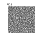
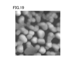
- 2 is an AFM image of the metal-based particle assembly 1-1 obtained in Example 1.
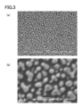
- 2 is an SEM image (10,000 times and 50000 times scale) when the metal-based particle assembly 1-2 obtained in Example 1 is viewed from directly above.
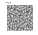
- 2 is an AFM image of a metal-based particle assembly 1-2 obtained in Example 1.
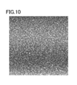
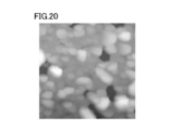
- 3 is an AFM image of the metal-based particle assembly 1-3 obtained in Example 1.
- 2 is an absorption spectrum of the metal-based particle assembly 1-2 obtained in Example 1. It is a schematic flowchart which shows the manufacturing method of a reference metal type particle aggregate.
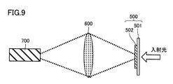
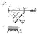
- FIG. 14A is a schematic diagram showing a measurement system for an emission spectrum of a photoexcited light emitting device
- FIG. 14B is a schematic cross-sectional view showing a photoexcited light emitting device having a metal particle aggregate and an insulating layer.
- FIG. 4 is a graph showing an emission enhancement effect in the photoexcited light emitting devices of Examples 5-1 to 5-4.
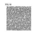
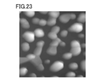
- 6 is an AFM image of a metal-based particle assembly 6 obtained in Example 6.
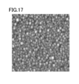
- 6 is an AFM image of a metal-based particle assembly 7 obtained in Example 7.
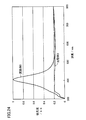
- 4 is an absorption spectrum of metal-based particle aggregates 6 and 7 obtained in Examples 6 and 7.
- 2 is an AFM image of a silver film H1 obtained in Comparative Example 1.
- 6 is an AFM image of a silver film H2 obtained in Comparative Example 2.
- 4 is an absorption spectrum of silver films H1 and H2 obtained in Comparative Examples 1 and 2.
- 6 is an AFM image of the metal-based particle assembly 8 obtained in Example 8.
- 6 is an AFM image of a silver film H3 obtained in Comparative Example 3. It is an absorption spectrum of the metal type particle aggregate 8 and the silver film H3 obtained in Example 8 and Comparative Example 3.
- the present invention relates to a method for producing a metal-based particle aggregate.
- the “metal-based particle aggregate” is an aggregate of a plurality of metal-based particles (particles made of a metal-based material), and the plurality of metal-based particles are two-dimensionally arranged apart from each other. Say what you are.
- a metal-based particle aggregate having a desired shape (the shape of the metal-based particles and the average interparticle distance, etc.) according to the purpose of use can be manufactured with good control. Can do.
- the “shape” of the metal-based particles refers to the “average particle diameter”, “average height”, and “aspect ratio” of the metal-based particles constituting the metal-based particle aggregate.
- the definitions of “average particle diameter”, “average height”, “aspect ratio” and “average interparticle distance” of the metal-based particles will be described later.
- the method for producing a metal-based particle assembly of the present invention includes the following steps: (A) a metal-based film forming step (first step) for forming a metal-based film having an average thickness of 50 nm or less on the substrate; and (B) a shape change of the metal-based film into a metal-based particle aggregate by heat treatment.
- Metal-based particle aggregate formation process (second process) including.
- FIG. 1 (a) is a schematic cross-sectional view for explaining this step, and FIGS. 1 (b) and (c) are metal-based particle aggregate forming steps (B) in the next step. It is a schematic sectional drawing for demonstrating.
- this step is a step of forming on the substrate 100 a metal film 250 (film made of a metal material) having an average thickness of 50 nm or less.
- the “average thickness” is a pointed object (tweezers, needle, etc.) provided with a peeling line (scratch) reaching the substrate 100 on the outer surface of the metallic film 250, and the metallic film 250 at this peeling line.
- An AFM image including the cross section of the substrate 100 and the interface between the metal film 250 and the substrate 100 is acquired, and the distance from the metal film 250 side surface of the substrate 100 to the outer surface of the metal film 250 is randomly selected based on the AFM image. The average value of these 10 points when 10 points are obtained.
- the average thickness of the metal-based film 250 is set to 50 nm. It is necessary to: The average thickness of the metal film 250 is preferably 40 nm or less, more preferably 30 nm or less, and still more preferably 20 nm or less. When the average thickness of the metal-based film 250 exceeds 50 nm, depending on the heat treatment temperature or the like in the metal-based particle assembly forming step (B), the shape may be partially changed into the metal-based particle assembly.
- At least most of the film becomes a continuous film, and it is difficult to convert the metal film 250 into a metal particle aggregate over the entire region.
- the heat treatment temperature in the metal-based particle assembly forming step (B) generally, the larger the average thickness of the metal-based film 250, the larger the average particle diameter and the higher the average metal height. A system particle aggregate is obtained.
- the average thickness of the preferable metal-based film 250 is 40 nm or less, the more preferable average thickness is 30 nm or less, and the more preferable average thickness is 20 nm or less.
- the metal-based particle aggregate having specific characteristics such as exhibiting extremely strong plasmon resonance as compared with the prior art by having a distance, etc., and suitable as an enhancement element for optical elements including light-emitting elements and photoelectric conversion elements This is because it can be formed with good control.
- the lower limit of the average thickness of the metal film 250 is not particularly limited, but a predetermined shape (average particle diameter of the metal particles 200 to 1600 nm, which is preferable for the metal particle aggregate suitable as an enhancement element of the optical element as described above, In order to achieve an average height of 55 to 500 nm, an aspect ratio of 1 to 8, and an average interparticle distance of 1 to 150 nm. 10 nm or more is more preferable, and 15 nm or more is more preferable.
- the metal-based film forming step (A) and the metal-based particle assembly forming step (B) twice or more the metal-based film at each time
- the lower limit value of the average thickness of 250 may be smaller than the preferable lower limit value.
- a preferred example of a method of forming the metal film 250 on the substrate 100 is a particle made of the same material as the metal material constituting the metal film 250 (hereinafter, this particle is used to form a metal particle aggregate “metal system”).
- This is a method of applying a coating solution containing “particles” to distinguish from “particles”.
- the coating solution is typically a dispersion in which the above particles are dispersed in a solvent. When the coating solution contains a solvent, the coating film is dried before the step (B) as necessary.
- Examples of the application method of the coating liquid include spin coating, bar coating, gravure coating, micro gravure coating, roll coating, rod coating, knife coating, air knife coating, kiss coating, and die coating.
- the spin coating method is preferable from the viewpoint of the high uniformity of the film thickness of the metal film 250 obtained.
- a web coating method such as a gravure coating method is preferable from the viewpoint that roll film formation is possible and productivity is excellent.
- the coating solution may be applied two or more times as necessary (for example, to achieve a desired average thickness).
- the coating liquid typically contains the above particles and a solvent.
- a commercially available product can be used, or a solution obtained by adding an additive such as a surfactant or a diluent solvent to the product can be used.
- a dispersion prepared by adding the particles and optionally added additives to the solvent may be used as the coating solution.
- the solvent various organic solvents, aqueous solvents such as water, or a mixture thereof can be used.
- the particles are not particularly limited as long as the particles include the metal-based material constituting the metal-based film 250 and may be modified such as surface treatment, but only from the metal-based material not subjected to any modification. It may be.
- the method of the present invention is also advantageous in that normal particles without any modification (for example, dispersions of particles that are generally not commercially available without any modification) can be used.
- the average particle size of the particles contained in the coating solution is usually 1 to 50 nm, more typically 1 to 40 nm, and preferably 1 to 20 nm. Within the range of 1 to 50 nm, although depending on the concentration of the particles in the coating solution, a metal film 250 having an average thickness of 50 nm or less is easily obtained. Note that even when the average particle diameter of the particles exceeds 50 nm, it is possible to obtain the metal-based film 250 having an average thickness of 50 nm or less. Therefore, particles having an average particle diameter exceeding 50 nm can also be used.
- the concentration of the particles in the coating solution is preferably 0.1 to 7% by weight.
- the average particle size of the particles and the application method (the type of application method such as spin coating method and bar coating method, and In this case, the average thickness tends to exceed 50 nm even if it is applied once, although it depends on the coating conditions such as the rotational speed in the spin coating method and the line speed in the roll coating method.
- the upper limit of the particle concentration is more preferably 5% by weight.
- a coating solution having a particle concentration of 0.1 to 7% by weight also allows the coating solution to be applied substantially evenly over the entire coating solution coating area without causing an excessively overcoated portion or an insufficiently coated portion. preferable. This further ensures that the metal film 250 is converted into a metal particle aggregate over the entire region.
- the particle concentration is extremely low, the density of the metal-based film 250 is extremely sparse, and the amount of the metal-based material that can be supported on the substrate is reduced by one coating, so that the metal-based particles are densely packed. It is difficult to obtain an arranged metal-based particle aggregate. Therefore, in order to obtain a metal particle aggregate having specific characteristics such as dense arrangement of metal particles (for example, an average interparticle distance of 1 to 150 nm) and exhibiting extremely strong plasmon resonance as compared with the prior art.
- the particle concentration is preferably 0.1% by weight or more as described above.
- the particle concentration of the coating liquid at each time may be less than 0.1% by weight.
- the particle concentration of the coating solution is more preferably 0.25% by weight or more, and further preferably 0.8% by weight or more. This is the number of repetitions of application of the coating liquid in one metal-based film formation step (A), and the number of repetitions of a series of steps including the metal-based film formation step (A) and the metal-based particle aggregate formation step (B).
- the web coating method when adopted as the coating method, it is easy to form a uniform metal film 250 having an average thickness of 50 nm or less, so the particle concentration of the coating solution should be 0.15 wt% or less. Is more preferable.
- the present invention in order to manufacture a metal-based particle aggregate having a desired shape according to the purpose of use (the shape of the metal-based particles and the average distance between the particles, etc.) with good control, It is important to set the average thickness to a predetermined thickness or less. And as a coating method for achieving this predetermined average thickness, various coating methods as listed above can be adopted in the present invention.
- the particle concentration of the coating solution is appropriately selected according to the coating method so that a predetermined average thickness can be achieved. In other words, even if a specific particle concentration of the coating liquid is unsuitable for a coating method, metal particles having a desired shape using this coating liquid by adopting another coating method in the present invention.
- the assembly can be manufactured with good control.
- the method of the present invention is also advantageous in that a highly productive coating method such as web coating can be employed.
- the method of forming the metal film 250 on the substrate 100 is a vapor deposition method in which vapor of a metal material is deposited on the substrate 100.
- the metal film 250 having an average thickness of 50 nm or less can be obtained by adjusting the deposition rate, the deposition time, and the like.
- the preferred average thickness is the same as above.
- a sputtering method, a plating method, or the like can be used as a method for forming the metal film 250 on the substrate 100.
- the absorption spectrum measurement using an absorptiometry is performed in the ultraviolet to A material that exhibits a plasmon resonance peak (hereinafter also referred to as a “plasmon peak”) that appears in the visible region is preferable.
- a noble metal such as gold, silver, copper, platinum, or palladium, or a metal such as aluminum or tantalum
- the noble metal or metal-containing alloy include metal compounds (metal oxides, metal salts, etc.) containing the noble metal or metal, among which noble metals such as gold, silver, copper, platinum, and palladium are preferable. From the viewpoint of low cost and low absorption (small imaginary part of dielectric function at visible light wavelength), silver is more preferable.
- the type of the system material is the use of the metal-based particle aggregate (for example, the type of the optical element when the metal-based particle aggregate is applied as an enhancement element of the optical element using the plasmon resonance effect), and It is preferable to select appropriately according to the absorption spectrum peak wavelength, emission spectrum peak wavelength, reflection spectrum peak wavelength, etc. of the active layer of the optical element to be enhanced.
- the material constituting the substrate 100 can be selected from a wide range, and in particular, a substrate on which metal-based particle assemblies are stacked (hereinafter also referred to as “metal-based particle assembly stacked substrate”) has its plasmon resonance effect.
- a substrate on which metal-based particle assemblies are stacked (hereinafter also referred to as “metal-based particle assembly stacked substrate”) has its plasmon resonance effect.
- metal-based particle assembly stacked substrate”) has its plasmon resonance effect.
- a substrate made of a non-conductive material This is because the plasmon resonance effect is reduced when electrons can be transferred between some or all of the metal-based particles via the substrate.
- non-conductive materials include glass, various inorganic insulating materials (SiO 2 , ZrO 2 , mica, etc.), various plastic materials, and the like.
- the surface of the substrate 100 on which the metal film 250 is formed is preferably as smooth as possible.
- the metal-based particle assembly laminated substrate is applied as, for example, an enhancement element of a light-emitting element, light can be extracted from the substrate surface (surface opposite to the metal-based particle assembly). It is preferable to use a light-transmitting substrate, and it is more preferable to use an optically transparent substrate.
- the outer surface of the metal-based film 250 formed on the substrate 100 by the method described above is not completely flat but has a certain uneven shape (FIG. 1A). reference).
- (B) Metal-based particle assembly forming step Referring to FIGS. 1B and 1C, this step is performed by heat-treating (annealing) a metal-based film 250 having an average thickness of 50 nm or less. This is a step of changing the shape to the metallic particle aggregate 200.
- the surface region 255 of the metal-based film 250 (this surface region is typically a metal oxide by heat) is thermally decomposed (see FIG. 1B).
- a shape change occurs where the metal film 250 is cut off at the valleys of the surface unevenness of the metal film 250, and the metal particle aggregate 200 composed of a plurality of metal particles 201 arranged independently of each other is formed. (See FIG. 1C).
- shape change in which the surface shape of the metal-based film 250 that has received heat changes before the metal-based film 250 is cut off and 2) formed metal-based particles.
- the shape of the obtained metal-based particle aggregate 200 depends on the heat treatment conditions, more specifically, the contribution of the main shape change and the secondary shape change depending on the heat treatment conditions.
- the temperature of the heat treatment is preferably 280 ° C. or higher, more preferably 285 ° C. or higher. Moreover, the temperature of heat processing is 600 degrees C or less normally, Preferably it is 580 degrees C or less.
- the heat treatment temperature is equal to or higher than the temperature at which the surface region 255 of the metal-based film 250 starts to thermally decompose (for example, about 150 to 200 ° C. when the surface region is made of silver oxide).
- the heat treatment temperature is less than 280 ° C., the shape change may take a long time, or the shape change may occur only with an extremely thin metal film 250 having an average thickness of less than 30 nm. Therefore, it tends to be difficult to obtain a metal particle aggregate having a desired shape.
- the heat treatment temperature By adjusting the heat treatment temperature, it is possible to produce a metal particle aggregate having a desired shape according to the purpose of use. For example, when the average thickness of the metal-based film 250 is about 30 nm or less, any of heat treatment in a low temperature region of about 280 to about 500 ° C. and heat treatment in a high temperature region of about 500 to about 600 ° C. It is possible to obtain a metal-based particle aggregate exhibiting a strong plasmon peak (showing a high plasmon resonance effect). At this time, as the heat treatment temperature is higher, a metal particle aggregate composed of metal particles having a larger average particle diameter and average height tends to be obtained.
- the secondary shape change of 3 that occurs after the metal-based particles 201 independent from each other are formed becomes conspicuous. In some cases, the metal-based particles 201 may disappear from the substrate 100.
- the average thickness of the metal film 250 is more than about 30 nm and less than 50 nm, a metal particle aggregate that exhibits a strong plasmon peak (shows a high plasmon resonance effect) by heat treatment in a high temperature region of about 500 to about 600 ° C. It is possible to get a body. Even when the average thickness of the metal-based film 250 is more than about 30 nm and not more than 50 ⁇ m, the higher the heat treatment temperature, the more likely the metal-based particle aggregate composed of metal-based particles having a larger average particle diameter and average height is obtained. is there. However, if the heat treatment time is excessively long, the secondary morphological change of the above 3) that occurs after the formation of the metal particles 201 independent from each other becomes significant, and finally the metal particles are formed on the substrate 100. 201 may disappear.
- the heat treatment time is usually several seconds to several hours, preferably 10 seconds to 1 hour, more preferably 30 seconds to 30 minutes. If the heat treatment time is excessively short, the shape change to the metal-based particle aggregate becomes insufficient, and if it is excessively long, the amount of heat treatment exceeding the time required to complete the shape change is wasted, and the process time is wasted. In some cases, the secondary morphological change of 3), which occurs after the metal particles 201 independent of each other are formed, becomes prominent, and the metal particles 201 may disappear from the substrate 100. In addition, when the heat treatment time at a relatively high temperature is excessively long, even if the average thickness of the metal-based film 250 is the same, the secondary shape change of the above 3) becomes remarkable.
- the environment during the heat treatment is not particularly limited, and may be any of an oxidizing atmosphere, a reducing atmosphere, a vacuum atmosphere, and an inert gas atmosphere.
- it can be performed in an air atmosphere.
- an oxidizing atmosphere, especially an air atmosphere is preferable.
- a metal-based particle assembly may be produced by repeating a series of steps including the metal-based film forming step (A) and the subsequent metal-based particle assembly forming step (B) twice or more. preferable.
- the metal particles by repeating the main shape change and the secondary shape change of the metal film 250 due to the supply of the metal material for forming the metal film 250 and the subsequent heat treatment, the metal particles The average particle size, average height, aspect ratio, and average interparticle distance of the metal-based particles are in a range that is difficult to carry out only by performing the above series of steps only once. It becomes easier to control.
- the metal-based particles can be disposed relatively densely (average interparticle distance). Can be reduced).
- the method of repeating the above-described series of steps is a metal particle aggregate that requires control of a more precise shape (the shape of the metal particles and the average distance between the particles), that is, in comparison with the conventional method. It has specific characteristics such as showing extremely strong plasmon resonance, and is suitable for the production of a metal-based particle aggregate described in detail below, which is suitable as an enhancement element for optical elements including light-emitting elements and photoelectric conversion elements.
- the first time is the same as the above steps (A) and (B).
- A1 a first metal-based film forming step of forming a first metal-based film having an average thickness of 50 nm or less on the substrate; and (B1) the first metal-based film is formed into a first metal-based film by heat treatment.
- the first metal-based particle aggregate obtained in the step (B1) and the second metal-based film formed thereon are integrated by heat treatment to form the second The shape changes to a metallic particle aggregate.
- the contents described above for the metal-based film forming process (A) and the metal-based particle aggregate forming process (B) are cited, respectively.
- the metal film forming conditions in the steps (A1) and (A2) and the heat treatment conditions in the steps (B1) and (B2) may be the same or different.
- the average thickness of the second metal film formed in the step (A2) is preferably 50 nm or less for the same reason as described above.
- the average thickness of the second metal-based film here is the same as that when forming on the first metal-based particle aggregate (for example, when applying a coating liquid, the same area, the same composition, The average thickness according to the above definition for the metal film when the metal film is formed on a flat substrate with the same coating method and the same coating amount.
- the metal-based particles are insulated from each other, in other words, non-conductive (metal) between adjacent metal-based particles.
- the system particle aggregate (film) is preferably non-conductive). This is because the plasmon resonance effect is reduced when electrons can be transferred between some or all of the metal-based particles. Therefore, for the same reason, it is preferable that the metal-based particles are reliably separated from each other and no conductive substance is interposed between the metal-based particles.
- the manufacturing method of this invention may include the process of forming an insulating layer in the surface of a metal type particle aggregate so that it may explain in full detail later.
- Metal-based particle assembly As described above, according to the production method of the present invention, it is possible to produce a metal-based particle aggregate having a desired shape (the shape of the metal-based particles and the average distance between the particles) with good control. Therefore, the present invention is useful as a method for producing a metal-based particle aggregate having specific characteristics such as exhibiting extremely strong plasmon resonance that is first manifested by precise shape control.
- This metal-based particle aggregate which is a plasmon material, can be suitably applied as an enhancement element for optical elements including light-emitting elements and photoelectric conversion elements, and can improve the luminous efficiency of the applied light-emitting elements and the conversion efficiency of the photoelectric conversion elements. This can be significantly improved as compared with the prior art.
- An example of the above-described metal-based particle aggregate suitable as an optical element enhancement element, which can be obtained by the production method of the present invention, has 30 or more metal-based particles arranged two-dimensionally apart from each other.
- the average particle diameter of the metallic particles is in the range of 200 to 1600 nm
- the average height is in the range of 55 to 500 nm
- the aspect ratio defined by the ratio of the average particle diameter to the average height is in the range of 1 to 8.
- a metal-based particle aggregate having any of the following characteristics.
- the metal-based particles constituting the metal-based particle aggregate are arranged so that the average distance (average interparticle distance) between the adjacent metal-based particles is within a range of 1 to 150 nm (hereinafter, This metal-based particle aggregate is also referred to as “metal-based particle aggregate [i]”), [Ii]
- the metal-based particle aggregate has a peak maximum wavelength on the longest wavelength side in the absorption spectrum in the visible light region, and the maximum wavelength is the same as the average particle diameter and the average height.
- this metal-based particle aggregate Compared to the reference metal particle aggregate (X) in which the metal particles made of the same material and the height are arranged so that the distance between the metal particles is all in the range of 1 to 2 ⁇ m, the range is 30 to 500 nm (Hereinafter, this metal-based particle aggregate is also referred to as “metal-based particle aggregate [ii]”).
- the metal-based particle aggregate has a peak maximum wavelength on the longest wavelength side in the absorption spectrum in the visible light region, and the absorbance at the maximum wavelength is the same as the average particle diameter, and the average high Than the reference metal particle aggregate (Y) in which the metal particles made of the same height and the same material are arranged so that the distance between the metal particles is all within the range of 1 to 2 ⁇ m. In comparison in terms of number, it is high (hereinafter, this metal-based particle aggregate is also referred to as “metal-based particle aggregate [iii]”).
- the average particle diameter and the average height are “same” as the reference metal-based particle aggregate (X) or (Y).
- the difference in average particle diameter is ⁇ 45 nm. It means that the difference in average height is within a range of ⁇ 15 nm.
- the range of action of localized plasmon resonance is within a very narrow range of 10 nm or less from the surface of the metal nanoparticles.
- the range of action of localized plasmon resonance is within a very narrow range of 10 nm or less from the surface of the metal nanoparticles.
- the distance between the metal nanoparticle and the molecule to be excited increases, the localized plasmon resonance no longer effectively affects the light emission enhancement effect, and the energy transfer of the Forster mechanism appears. This is because if the range (1 nm to 10 nm) is exceeded, almost no light emission enhancement effect can be obtained.
- the distance between the metal nanoparticles effective for obtaining an effective light emission enhancement effect and the excited molecule is set to 10 nm or less.
- the enhancement effect of the optical element using the localized plasmon resonance phenomenon of the conventional metal nanoparticles or aggregates thereof is not always satisfactory due to the limitation of the range of action of localized plasmon resonance. That is, when the optical element has an active layer having a thickness of several tens of nanometers or more (for example, a light emitting layer of a light emitting element, a light absorbing layer of a photoelectric conversion element), the metal nanoparticles are temporarily close to the active layer, Or even if it can be placed inside, the direct enhancement effect by localized plasmon resonance can be obtained only in a part of the active layer, so the luminous efficiency and conversion efficiency improvement effect is partial. Met.
- the metal particle aggregates [i] to [iii] that can be obtained by the production method of the present invention are considered that the metal particles constituting the metal particle aggregates generally have a small light emission enhancing effect.
- the metal particles constituting the metal particle aggregates generally have a small light emission enhancing effect.
- plasmons that exhibit extremely strong plasmon resonance and are significantly elongated due to having a specific shape, etc.
- the range of action of resonance (the range covered by the plasmon enhancement effect) is shown.
- metal-based particle aggregates [i] to [iii] will be described in detail.
- the metal-based particle aggregate [i] is extremely advantageous in the following points.
- the intensity of the plasmon resonance indicated by the metal-based particle aggregate [i] is not a mere sum of the localized plasmon resonances exhibited by individual metal-based particles at a specific wavelength, but is higher than that. That is, when 30 or more metal particles having a predetermined shape are densely arranged at the predetermined interval, individual metal particles interact with each other, and extremely strong plasmon resonance is expressed. This is considered to be expressed by the interaction between the localized plasmons of the metal-based particles.
- a plasmon peak is observed as a peak in the ultraviolet to visible region.
- the metal-based particle aggregate [i] formed on the glass substrate has a maximum wavelength of the plasmon peak on the longest wavelength side in the visible light region when the absorption spectrum is measured. Can be 0.4 or more, further 0.7 or more, and even 0.9 or more.
- the absorption spectrum of the metal-based particle aggregate is measured by absorptiometry using a sample formed on a glass substrate as a measurement sample.
- the absorption spectrum is the back side of the glass substrate on which the metal particle aggregates are laminated (the side opposite to the metal particle aggregates), and the ultraviolet to visible light region from the direction perpendicular to the substrate surface.
- the plasmon resonance action range (the range in which the plasmon enhances the effect) is significantly extended. Such an elongation action is also considered to be manifested by the interaction between localized plasmons of metal-based particles generated by densely arranging 30 or more predetermined-shaped metal particles at a predetermined interval. According to the metal-based particle aggregate [i], it is possible to extend the plasmon resonance action range, which is conventionally limited to the range of about the Forster distance (about 10 nm or less), to about several hundred nm, for example.
- the extension of the plasmon resonance operating range as described above is extremely advantageous for enhancing optical elements such as light emitting elements and photoelectric conversion elements. That is, due to the significant extension of this working range, even if the active layer has a thickness of several tens of nanometers or more, it becomes possible to enhance the entire active layer, thereby enhancing the optical element. (Emission efficiency, conversion efficiency, etc.) can be significantly improved.
- the plasmon material has to be arranged so that the distance from the active layer is within the range of the Förster distance.
- the active layer Therefore, for example, the enhancement effect by plasmon resonance can be obtained even if they are arranged at a position 10 nm, further several tens of nm (for example, 20 nm), or even several hundred nm apart.
- the metal-based particle aggregate can be disposed in the vicinity of the light extraction surface considerably away from the light-emitting layer. It is possible to suppress the total reflection at the interfaces of the various light emitting element constituting layers that pass through until the light emitted from the light reaches the light extraction surface, so that the light extraction efficiency can be improved.
- the metal particle aggregate [i] alone uses such a large-sized metal particle in which a dipole-type localized plasmon alone is difficult to occur in the visible light region.
- a specific number or more of metal-based particles although it is necessary to have a predetermined shape
- an extremely large number of the metal-based particles included in the large-sized metal particles The surface free electrons can be effectively excited as plasmons, and it is possible to realize remarkably strong plasmon resonance and a significant extension of the range of action of plasmon resonance.
- the metal particle aggregate [i] has a structure in which a specific number or more of relatively large metal particles having a specific shape are two-dimensionally spaced apart at a specific interval.
- the maximum wavelength of the plasmon peak can show a specific shift depending on the average particle diameter of metal-based particles and the average distance between particles. Specifically, the maximum wavelength of the plasmon peak on the longest wavelength side in the visible light region shifts to the short wavelength side (blue shift) as the average particle size of the metal-based particles increases with a constant average interparticle distance. To do. Similarly, as the average particle size of large metal particles is kept constant and the distance between the average particles is decreased (when metal particles are arranged more densely), the maximum of the plasmon peak on the longest wavelength side in the visible light region The wavelength shifts to the short wavelength side. This peculiar phenomenon is the Mie scattering theory generally accepted for plasmon materials [in accordance with this theory, the maximum wavelength of the plasmon peak shifts to the longer wavelength side (red shift) as the particle size increases. ] Is against this.
- the unique blue shift as described above also has a structure in which the metal-based particle aggregate [i] has a structure in which large-sized metal particles are densely arranged at specific intervals. This is thought to be due to the interaction between the localized plasmons of.
- the metal-based particle aggregate [i] (in a state of being laminated on the glass substrate) has the longest absorption spectrum in the visible light region measured by the absorptiometry according to the shape of the metal-based particles and the average interparticle distance.
- the plasmon peak on the wavelength side can exhibit a maximum wavelength in a wavelength region of 350 to 550 nm, for example.
- the metal-based particle aggregate [i] is typically about 30 to 500 nm (for example 30 to 30 nm) as compared with the case where the metal-based particles are arranged with a sufficiently long inter-particle distance (for example 1 ⁇ m). 250 nm) blue shift can occur.
- Such a metal-based particle aggregate in which the maximum wavelength of the plasmon peak is blue-shifted compared to the conventional one is extremely advantageous, for example, in the following points. That is, while there is a strong demand for a blue (or near-wavelength region, hereinafter the same) luminescent material (especially a blue phosphorescent material) that exhibits high luminous efficiency, development of such a material that can withstand practical use is currently underway. However, it is difficult to use a blue light emitting material with relatively low luminous efficiency by applying, for example, a metallic particle aggregate [i] having a plasmon peak in the blue wavelength region as an enhancement element to a light emitting element. However, the luminous efficiency can be increased to a sufficient level. In addition, when applied to photoelectric conversion elements (solar cell elements, etc.), for example, the wavelength region that could not be used in the active layer itself can be effectively utilized by blue shifting the resonance wavelength, thereby improving the conversion efficiency. obtain.
- the average particle diameter of the metal-based particles is in the range of 200 to 1600 nm. In order to effectively obtain the effects (1) to (3), preferably 200 to 1200 nm, more preferably 250 to 500 nm, and still more preferably Is in the range of 300 to 500 nm.
- the average particle diameter of the metal-based particles is preferably selected appropriately depending on the type of optical element to which the metal-based particle aggregate is applied as an enhancement element and the type of material constituting the metal-based particles.
- the metal particle aggregate [i] has an extremely strong plasmon resonance and plasmon resonance action by densely arranging a predetermined number (30) or more of such large metal particles at a predetermined interval. The remarkable extension of the range and further the effect (3) are realized.
- the average particle size of the metal-based particles means that 10 particles are randomly selected in the SEM observation image from directly above the metal-based particle assembly in which the metal-based particles are two-dimensionally arranged, and each particle image includes Randomly draw 5 tangential diameters (however, any straight line with a tangential diameter can only pass through the interior of the particle image, one of which is only the interior of the particle and is the longest drawable line)
- the average value of the 10 selected particle sizes when the average value is the particle size of each particle.
- the tangent diameter is defined as a perpendicular line connecting the interval (projection image) of a particle between two parallel lines in contact with it (Nikkan Kogyo Shimbun, “Particle Measurement Technology”, 1994, page 5). .
- the average height of the metal-based particles is in the range of 55 to 500 nm, and in order to effectively obtain the effects (1) to (3), preferably in the range of 55 to 300 nm, more preferably 70 to 150 nm. It is.
- the average height of the metal-based particles refers to 10 measured values when 10 particles are randomly selected in the AFM observation image of the metal-based particle aggregate and the heights of these 10 particles are measured. Average value.
- the aspect ratio of the metal-based particles is in the range of 1 to 8, and it is preferable that the metal-based particle aggregate is appropriately selected depending on the type of optical element to which the metal-based particle aggregate is applied as an enhancement element.
- the metal-based particles when used as an enhancement element of a light emitting element, the metal-based particles tend to have a flat shape, and in this case, in order to obtain a higher enhancement effect, the aspect ratio is preferably 2 to 8. 2.5 to 8 is more preferable.
- the metal particles when used as an enhancement element of a photoelectric conversion element, in order to obtain a higher enhancement effect, the metal particles tend to be more preferable as they are closer to a true sphere.
- the aspect ratio of the metal-based particles is defined by the ratio of the average particle diameter to the average height (average particle diameter / average height).
- the surface of the metal-based particles is preferably a smooth curved surface, but the surface may contain some minute irregularities (roughness).
- the metal particles may be indefinite.
- the variation in size between the metal-based particles is as small as possible.
- the distance between the large particles is increased, and it is preferable that the interaction between the large particles is facilitated by filling the space between the small particles.
- the metal-based particles are arranged so that the average distance (average interparticle distance) between the adjacent metal-based particles is in the range of 1 to 150 nm.
- the average interparticle distance is preferably in the range of 1 to 100 nm, more preferably 1 to 50 nm, and even more preferably 1 to 20 nm in order to effectively obtain the effects (1) to (3).
- the average interparticle distance is less than 1 nm, electron transfer based on the Dexter mechanism occurs between particles, which is disadvantageous in terms of deactivation of localized plasmons.
- the average interparticle distance means that 30 particles are randomly selected in an SEM observation image from directly above a metal particle aggregate in which metal particles are two-dimensionally arranged, and each selected particle is adjacent to each other. It is the average value of the interparticle distances of these 30 particles when the interparticle distance with the matching particles is obtained.
- the inter-particle distance between adjacent particles is a value obtained by measuring the distances between all adjacent particles (the distance between the surfaces) and averaging them.
- the number of metal particles contained in the metal particle aggregate [i] is 30 or more, preferably 50 or more.
- the number of metal-based particles contained in the metal-based particle aggregate [i] is, for example, in light of the general element area of the optical element, It can be 300 or more, and further 17500 or more.
- the number density of metal particles in the metal particle aggregate [i] is preferably 7 particles / ⁇ m 2 or more, and more preferably 15 particles / ⁇ m 2 or more.
- the metal-based particles are insulated from each other, that is, non-conductive with respect to adjacent metal-based particles (metal-based particle aggregate (film)). Is preferably non-conductive).
- Metal-based particle aggregate [ii] The metal-based particle aggregate [ii] is extremely advantageous in the following points.
- the maximum wavelength of the plasmon peak on the longest wavelength side exists in a specific wavelength region.
- the maximum wavelength of the plasmon peak is 30 to more than the maximum wavelength of the reference metal-based particle aggregate (X) described later.
- the wavelength is shifted to the short wavelength side (blue shift) in the range of 500 nm (for example, in the range of 30 to 250 nm).
- the maximum wavelength of the plasmon peak is in the range of 350 to 550 nm.
- Such a metal-based particle aggregate [ii] that can have a plasmon peak in blue or in the vicinity wavelength region thereof is extremely useful for enhancing light emission of a light-emitting element using a light-emitting material in blue or in the vicinity wavelength region,
- a light-emitting device including such a metal-based particle aggregate [ii] even when a blue light-emitting material having a relatively low light emission efficiency is used, the light emission efficiency can be enhanced to a sufficient level.
- a photoelectric conversion element solar cell element, etc.
- the blue shift has a structure in which the metal-based particle aggregate [ii] has a structure in which a specific number or more of large-sized metal-based particles having a specific shape are two-dimensionally spaced. This is thought to be due to the interaction between the local plasmons of the system particles.
- the reference metal-based particle aggregate (X) is obtained by replacing the metal-based particles A having the same average particle diameter, the same particle size, the same height as the average height, and the same material with the metal particle aggregates to be subjected to absorption spectrum measurement.
- the absorption spectrum waveform of the reference metal-based particle aggregate (X) includes the particle size and height of the metal-based particle A, the dielectric function of the material of the metal-based particle A, and the dielectric function of the medium (for example, air) around the metal-based particle A. It is also possible to theoretically calculate by the 3D-FDTD method using the dielectric function of the substrate (for example, a glass substrate).
- the metal-based particle aggregate [ii] has a structure in which a specific number or more of relatively large metal-based particles having a specific shape are arranged two-dimensionally apart from each other, (II) Extremely strong plasmon resonance can be exhibited (similar to the effect (1) of the metal-based particle aggregate [i]), and (III) the range of action of plasmon resonance (the range over which the plasmon enhances) is significantly extended. (Similar to the effect (2) of the metal-based particle aggregate [i]).
- the absorbance at the maximum wavelength of the plasmon peak on the longest wavelength side in the visible light region is 0.4 or more, and further 0 .7 or more, and even 0.9 or more.
- the specific configuration of the metal-based particle aggregate [ii] is the specific configuration of the metal-based particle aggregate [i] (the material of the metal-based particles, the average particle diameter, the average height, the aspect ratio, the average interparticle distance, the metal The number of the system particles, the non-conductivity of the metal-based particle aggregate, etc.) can be basically the same. Definitions of terms such as average particle diameter, average height, aspect ratio, and average interparticle distance are the same as those for the metal-based particle aggregate [i].
- the average particle diameter of the metal-based particles is in the range of 200 to 1600 nm. In order to effectively obtain the effects (I) to (III), preferably 200 to 1200 nm, more preferably 250 to 500 nm, and still more preferably Is in the range of 300 to 500 nm. By forming an aggregate in which a predetermined number (30) or more of such large metal particles are two-dimensionally arranged, it is possible to realize extremely strong plasmon resonance and a significant extension of the plasmon resonance operating range. Further, in order to develop the above feature [ii] (plasmon peak shift to the short wavelength side), the metal particles must have an average particle size of 200 nm or more, preferably 250 nm or more. . The average particle diameter of the metal-based particles is preferably selected appropriately depending on the type of optical element to which the metal-based particle aggregate is applied as an enhancement element and the type of material constituting the metal-based particles.
- the maximum wavelength of the plasmon peak on the longest wavelength side in the visible light region depends on the average particle diameter of the metal-based particles. That is, when the average particle diameter of the metal-based particles exceeds a certain value, the maximum wavelength of the plasmon peak shifts (blue shift) to the short wavelength side.
- the average height of the metal-based particles is in the range of 55 to 500 nm. In order to effectively obtain the effects (I) to (III), the average height is preferably in the range of 55 to 300 nm, more preferably in the range of 70 to 150 nm. It is.
- the aspect ratio of the metal-based particles is in the range of 1 to 8, and as with the metal-based particle aggregate [i], it is appropriate depending on the type of optical element to which the metal-based particle aggregate is applied as an enhancement element. It is preferable to select.
- the metal particles are preferably arranged so that the average interparticle distance is in the range of 1 to 150 nm. More preferably, it is in the range of 1 to 100 nm, still more preferably 1 to 50 nm, and particularly preferably 1 to 20 nm.
- the metal-based particles densely as described above, the interaction between the local plasmons of the metal-based particles is effectively generated, and the effects (I) to (III) are easily exhibited. Since the maximum wavelength of the plasmon peak depends on the average interparticle distance of the metal-based particles, the degree of blue shift of the plasmon peak on the longest wavelength side and the maximum wavelength of the plasmon peak are controlled by adjusting the average interparticle distance. Is possible. When the average interparticle distance is less than 1 nm, electron transfer based on the Dexter mechanism occurs between particles, which is disadvantageous in terms of deactivation of localized plasmons.
- the number of metal particles contained in the metal particle aggregate [ii] is 30 or more, preferably 50 or more.
- the number of metal-based particles included in the metal-based particle aggregate [ii] is, for example, It can be 300 or more, and further 17500 or more.
- the number density of metal particles in the metal particle aggregate [ii] is preferably 7 particles / ⁇ m 2 or more, and more preferably 15 particles / ⁇ m 2 or more.
- Metal-based particle aggregate [iii] Metal-based particle aggregate [iii]
- the metal-based particle aggregate [iii] is extremely advantageous in the following points.
- the reference at the maximum wavelength of the peak on the longest wavelength side in the visible light region, which is a plasmon peak, can be regarded as an aggregate in which metal-based particles are simply aggregated without any interparticle interaction. Since it is larger than the metal-based particle aggregate (Y) and thus exhibits extremely strong plasmon resonance, when applied to a light-emitting element, a stronger emission enhancement effect is obtained compared to the case of using a conventional plasmon material. As a result, the luminous efficiency can be dramatically increased. Further, when applied to a photoelectric conversion element, this conversion efficiency can be dramatically increased. Such strong plasmon resonance is considered to be expressed by the interaction between localized plasmons of metal-based particles.
- the absorbance at the maximum wavelength of the plasmon peak on the longest wavelength side in the visible light region is 0.4 or more, further 0.7 or more, and even more preferably 0.8. It can be 9 or more.
- the reference metal-based particle aggregate (Y) is obtained by replacing the metal-based particles B having the same average particle size, average particle size, height and same material as the average particle diameter of the metal-based particle aggregate that is the target of absorption spectrum measurement.
- the following is described.
- an absorption spectrum of the reference metal-based particle aggregate (Y) converted so as to have the same number of metal-based particles is obtained, and the absorbance at the maximum wavelength of the peak on the longest wavelength side in the absorption spectrum is used for comparison.
- the absorption spectrum of each of the metal-based particle assembly and the reference metal-based particle assembly (Y) is obtained, and the absorbance at the maximum wavelength of the peak on the longest wavelength side in each of the absorption spectra is expressed as the coverage ratio. The value divided by (the coverage of the substrate surface with the metal particles) is calculated and compared.
- the metal particle aggregate [iii] has a structure in which a specific number or more of relatively large metal particles having a specific shape are arranged two-dimensionally apart from each other, (B) The action range of plasmon resonance (the range in which the enhancement effect by plasmons can be extended) can be significantly extended (similar to the effect (2) of the metal-based particle aggregate [i] above), and (c) the maximum wavelength of the plasmon peak Can exhibit a peculiar shift (similar to the effect (3) of the metal-based particle aggregate [i]).
- the metal-based particle aggregate [iii] (in the state of being laminated on the glass substrate) has the longest absorption spectrum in the visible light region measured by the absorptiometry according to the shape of the metal-based particles and the average interparticle distance.
- the plasmon peak on the wavelength side can exhibit a maximum wavelength in a wavelength region of 350 to 550 nm, for example.
- the metal-based particle aggregate [iii] is typically about 30 to 500 nm (for example, 30 to 30 nm) as compared with the case where the metal-based particles are arranged with a sufficiently long inter-particle distance (for example, 1 ⁇ m). 250 nm) blue shift can occur.
- the specific configuration of the metal-based particle aggregate [iii] is the specific configuration of the metal-based particle aggregate [i] (the material of the metal-based particles, the average particle diameter, the average height, the aspect ratio, the average interparticle distance, the metal The number of the system particles, the non-conductivity of the metal-based particle aggregate, etc.) can be basically the same. Definitions of terms such as average particle diameter, average height, aspect ratio, and average interparticle distance are the same as those for the metal-based particle aggregate [i].
- the average particle diameter of the metal-based particles is in the range of 200 to 1600 nm, and the characteristics of [iii] above (the absorbance at the maximum wavelength of the plasmon peak on the longest wavelength side is that of the reference metal-based particle aggregate (Y)).
- it is preferably in the range of 200 to 1200 nm, more preferably 250 to 500 nm, and still more preferably 300 to 500 nm. .
- it is important to form relatively large metal particles, and by forming an aggregate in which a predetermined number (30) or more of large metal particles are two-dimensionally arranged, extremely strong plasmons are obtained.
- the average particle diameter of the metal-based particles is preferably selected appropriately depending on the type of optical element to which the metal-based particle aggregate is applied as an enhancement element and the type of material constituting the metal-based particles.
- the average height of the metal-based particles is in the range of 55 to 500 nm, and in order to effectively obtain the characteristics of [iii] and further the effects (a) to (c), preferably 55 to 300 nm, More preferably, it is in the range of 70 to 150 nm.
- the aspect ratio of the metal-based particles is in the range of 1 to 8, and as with the metal-based particle aggregate [i], it is appropriate depending on the type of optical element to which the metal-based particle aggregate is applied as an enhancement element. It is preferable to select.
- the metal-based particles constituting the metal-based particle aggregate [iii] are as uniform in shape (average particle diameter, average height, aspect ratio) as possible.
- the plasmon peak is sharpened, and accordingly, the absorbance of the plasmon peak on the longest wavelength side is higher than that of the reference metal-based particle aggregate (Y). It becomes easy.
- Reduction of variation in shape between metal-based particles is advantageous from the viewpoint of uniformity of plasmon resonance strength in the plane of the metal-based particle assembly.
- the distance between the large particles increases, and the interaction between the large particles is facilitated by filling the space between the small particles. It is preferable.
- the metal particles are preferably arranged so that the average interparticle distance is in the range of 1 to 150 nm. More preferably, it is in the range of 1 to 100 nm, still more preferably 1 to 50 nm, and particularly preferably 1 to 20 nm.
- the average interparticle distance is less than 1 nm, electron transfer based on the Dexter mechanism occurs between particles, which is disadvantageous in terms of deactivation of localized plasmons.
- the number of metal particles contained in the metal particle aggregate [iii] is 30 or more, preferably 50 or more.
- the number of metal-based particles included in the metal-based particle aggregate [iii] is, for example, It can be 300 or more, and further 17500 or more.
- the number density of the metal particles in the metal particle aggregate [iii] is preferably 7 particles / ⁇ m 2 or more, and more preferably 15 particles / ⁇ m 2 or more.
- the metal-based particle aggregate [iii] can be obtained by controlling the metal species and shape of the metal-based particles constituting the metal-based particle aggregate and the average distance between the metal-based particles.
- the metal-based particle aggregate suitable as an enhancement element of an optical element obtainable by the production method of the present invention preferably has any two or more features of [i] to [iii], more preferably It has all the features [i] to [iii].
- the production method of the present invention includes an insulating layer forming step after the metal-based particle assembly forming step (B), and covers the surface of each metal-based particle on the thin film of the metal-based particle assembly. May be formed.
- Such an insulating layer is not only preferable for ensuring the non-conductivity (non-conductivity between metal-based particles) of the metal-based particle assembly described above, but also when the metal-based particle assembly is applied to an optical element. Also preferred. That is, in an optical element such as an electric energy-driven light-emitting element or photoelectric conversion element, a current flows in each layer constituting the element, but if the current flows in the metal-based particle aggregate, the enhancement effect by plasmon resonance is sufficient. May not be obtained.
- the material constituting the insulating layer is not particularly limited as long as it has good insulating properties.
- SiO 2 or Si 3 N 4 Etc. can be used.
- the thickness of the insulating layer is not particularly limited as long as desired insulating properties are ensured, but an active layer when applied to an optical element as described later (for example, a light emitting layer of a light emitting element or a light absorbing layer of a photoelectric conversion element). Since the distance between the metal particle aggregate and the metal-based particle aggregate is preferably as short as possible, it is preferable that the distance is as small as possible within a range in which desired insulation is ensured.
- the metal-based particle aggregate obtained by the production method of the present invention can be incorporated into various optical elements in a state of being integrated with a substrate used when the metal particle aggregate is produced.
- the metal-based particle aggregates [i] to [iii] that can be obtained by the production method of the present invention exhibit extremely strong plasmon resonance, and further, the range of action of plasmon resonance (range of enhancement effect by plasmon)
- the entire active layer having a thickness of 10 nm or more, further 20 nm or more, and even more can be enhanced.
- the active layer disposed at a position separated by, for example, 10 nm, further several tens of nm (for example, 20 nm), or even several hundred nm or more can be enhanced extremely effectively.
- the distance between the active layer and the metal-based particle aggregate is preferably 100 nm or less, more preferably 20 nm or less, and further preferably 10 nm or less.
- the maximum wavelength of the emission wavelength (for example, in the case of a light-emitting element) or the absorption wavelength (for example in the case of a photoelectric conversion element) exhibited by the active layer matches or is close to the maximum wavelength of the plasmon peak of the metal-based particle aggregate.
- the maximum wavelength of the plasmon peak of the metal particle aggregate can be controlled by adjusting the metal species, average particle diameter, average height, aspect ratio and / or average particle distance of the metal particles constituting the metal particle aggregate.
- the light emitting layer is, for example, 1) composed of a monomolecular film in which dye molecules are arranged in a plane, 2) composed of a matrix doped with dye molecules, 3) composed of a light emitting low molecule, 4) It can be made of a light-emitting polymer.
- the light emitting layer of 1) can be obtained by a method of removing the solvent after spin-coating the dye molecule-containing liquid.
- the dye molecule include rhodamine 101, rhodamine 110, rhodamine 560, rhodamine 6G, rhodamine B, rhodamine 640 and rhodamine 700 sold by Exciton, and coumarin 503 available from Exciton. Including coumarin-based pigments.
- the light emitting layer of 2) can be obtained by a method of removing a solvent after spin-coating a liquid containing a dye molecule and a matrix material.
- a transparent polymer such as polyvinyl alcohol or polymethyl methacrylate can be used.
- Specific examples of the dye molecule can be the same as those in the light emitting layer of 1).
- the light emitting layer 3) can be obtained by a dry or wet film forming method including a spin coating method and a vapor deposition method.
- Specific examples of the light-emitting small molecule include tris (8-quinolinolato) aluminum complex [tris (8-hydroxyquinoline) aluminum complex; Alq 3 ], bis (benzoquinolinolato) beryllium complex [BeBq] and the like.
- the light emitting layer of 4) can be obtained by a wet film forming method using a light emitting polymer-containing liquid such as a spin coat method.
- a light emitting polymer-containing liquid such as a spin coat method.
- Specific examples of the light emitting polymer include ⁇ -conjugated polymers such as F8BT [poly (9,9-dioctylfluorene-alt-benzothiadiazole)], poly (p-phenylenevinylene), polyalkylthiophene, and the like.
- the metal-based particle aggregates [i] to [iii] have been mainly described as the metal-based particle aggregates obtainable by the production method of the present invention, but the metal-based particle aggregates obtainable by the production method of the present invention have been described above.
- a particle aggregate is one in which any one or more of the number of metal particles, shape of metal particles (average particle diameter, average height, aspect ratio), and average interparticle distance are not within the above range. It may be.
- Such metal-based particle aggregates may not be as advantageous as the metal-based particle aggregates [i] to [iii] in terms of the enhancement effect by plasmons, but they are still equivalent to conventional plasmon materials. Or, since it can exhibit a further enhancement effect, it can be applied to an enhancement element of an optical element.
- the metal-based particle assembly and metal-based particle assembly laminated substrate of the present invention can also be used for analysis applications and color material applications.
- the analytical application includes application to surface enhanced Raman spectroscopy using surface enhanced Raman scattering.
- Examples of the color material use include use as a color imparting material for various articles (automobiles, ceramics, etc.).
- color rendering that is difficult to achieve with pigments and pigments can be achieved.
- Examples of the color filter include a filter that transmits only light having a specific wavelength or blocks light having a specific wavelength.
- the average thickness of the metal-based film (silver film) before the heat treatment is such that a peeling line (scratch) reaching the substrate is provided on the outer surface of the metal-based film with tweezers, and the cross-section of the metal-based film and the metal-based film at this peeling line 10 points when a distance from the metal film side surface of the substrate to the outer surface of the metal film is randomly determined based on this AFM image including the interface between the substrate and the substrate It was calculated as an average value.
- Example 1 (1) Preparation of metal-based particle aggregate Silver nanoparticle aqueous dispersion (manufactured by Mitsubishi Paper Industries, Ltd., silver nanoparticle concentration: 25% by weight, average particle diameter of silver nanoparticles: 15 nm) with pure water, silver nanoparticle concentration was diluted to 2% by weight. Next, after adding 1% by volume of the surfactant to the diluted silver nanoparticle aqueous dispersion and stirring well, 80% by volume of acetone was added to the obtained silver nanoparticle aqueous dispersion. The mixture was sufficiently stirred at room temperature to prepare a coating solution.
- Silver nanoparticle aqueous dispersion manufactured by Mitsubishi Paper Industries, Ltd., silver nanoparticle concentration: 25% by weight, average particle diameter of silver nanoparticles: 15 nm
- silver nanoparticle concentration was diluted to 2% by weight.
- 80% by volume of acetone was added to the obtained silver nanoparticle aqueous dispersion. The mixture was sufficiently stirred at room temperature to prepare
- the above coating solution was spin-coated at 1000 rpm on a 1 mm thick soda glass substrate whose surface was wiped with acetone, and then allowed to stand in the atmosphere for 1 minute.
- the average thickness of the obtained silver film was 21.6 nm.
- the soda glass substrate on which the silver film was formed was placed in an electric furnace at 550 ° C. and heat-treated (fired) for 40 seconds in an air atmosphere to obtain a metal-based particle aggregate 1-1.
- the above coating solution was spin-coated again at 1000 rpm on the obtained metal-based particle assembly 1-1, and left in the atmosphere for 1 minute. Thereafter, the soda glass substrate on which the silver film and the metal-based particle aggregate 1-1 are formed is placed in an electric furnace at 550 ° C. and subjected to heat treatment (firing) for 40 seconds in an air atmosphere. 2 was obtained.
- the above coating solution was spin-coated again at 1000 rpm on the obtained metal-based particle assembly 1-2, and left in the air for 1 minute. Thereafter, the soda glass substrate on which the silver film and the metal-based particle aggregate 1-2 are formed is placed in an electric furnace at 550 ° C. and subjected to heat treatment (firing) for 40 seconds in an air atmosphere. 3 was obtained.
- FIG. 2 is an AFM image showing the metal-based particle assembly 1-1.
- “VN-8010” manufactured by Keyence Corporation was used for AFM image shooting (the same applies hereinafter).
- the image size of this AFM image is 5 ⁇ m ⁇ 5 ⁇ m (the same applies to the following AFM images). From this AFM image, the average height of the silver particles constituting the metal-based particle aggregate 1-1 was determined to be 62.4 nm.
- FIG. 3 is an SEM image when the metal-based particle aggregate 1-2 is viewed from directly above.
- FIG. 3A is an enlarged image on a 10000 times scale
- FIG. 3B is an enlarged image on a 50000 times scale.
- FIG. 4 is an AFM image showing the metal-based particle aggregate 1-2. From the SEM image shown in FIG. 3, the average particle size of the silver particles constituting the metal-based particle assembly 1-2 was determined to be 293 nm, and the average inter-particle distance was 107.8 nm. From the AFM image shown in FIG. 4, the average height was determined to be 93.0 nm.
- the aspect ratio (average particle diameter / average height) of the silver particles is calculated to be 3.15, and it can be seen from the acquired image that the silver particles have a flat shape. Furthermore, it can be seen from the SEM image that the metal-based particle aggregate 1-2 has about 3.13 ⁇ 10 10 (about 12.5 particles / ⁇ m 2 ) silver particles.
- FIG. 5 is an AFM image showing the metal-based particle aggregate 1-3. From this AFM image, the average height of the silver particles constituting the metal-based particle aggregate 1-3 was determined to be 140.7 nm.
- the conductivity of the metal-based particle aggregates 1-1 to 1-3 was confirmed by connecting a tester [Multimeter (“E2378A” manufactured by Hewlett-Packard Co.)] to the surface thereof. was confirmed.
- FIG. 6 is an absorption spectrum measured by absorptiometry of the metal-based particle assembly 1-2 (in a state of being laminated on the substrate).
- Non-patent literature K. Lance Kelly, et al., "The Optical Properties of Metal Nanoparticles: The Influence of Size, Shape, and Dielectric Environment", The Journal of Physical Chemistry B, 2003, 107, 668)
- the flat silver particles when they are not aggregates but alone, they have a plasmon peak around 550 nm when the average particle size is 200 nm and around 650 nm when the average particle size is 300 nm. It is common.
- the metal-based particle aggregate 1-2 has the longest wavelength in the visible light region, as shown in FIG. 6, although the average particle diameter of the silver particles constituting the metal particle aggregate 1-2 is about 300 nm (293 nm). It can be seen that the maximum wavelength of the plasmon peak on the side is 488 nm, shifted to the short wavelength side. This phenomenon is considered to be because a predetermined number or more of silver particles have the above-mentioned predetermined shape, and the silver particles are preferably arranged very densely. It can also be seen that the absorbance at the maximum wavelength of the plasmon peak on the longest wavelength side in the visible light region is about 0.45, indicating strong plasmon resonance.
- the absorption spectrum shown in FIG. 6 is on the back side of the glass substrate on which the metal particle aggregates are laminated (on the side opposite to the metal particle aggregates), and is ultraviolet to visible from the direction perpendicular to the substrate surface. Irradiated with light in the light region and transmitted to the metallic particle aggregate side in all directions, the transmitted light intensity I is the same thickness and material as the substrate, and the metallic particle aggregate is not laminated. It is obtained by irradiating the same incident light from the direction perpendicular to the surface of the substrate and measuring the intensity I 0 of transmitted light in all directions transmitted from the opposite side of the incident surface using an integrating sphere spectrophotometer. It is what was done.
- a substrate on which the reference metal-based particle aggregate was laminated was produced according to the method shown in FIG.
- a resist (ZEP520A manufactured by Nippon Zeon Co., Ltd.) was spin-coated on approximately the entire surface of a substrate 100 made of soda glass having a length of 5 cm and a width of 5 cm (FIG. 7A).
- the thickness of the resist 400 was about 120 nm.
- a circular opening 401 was formed in the resist 400 by electron beam lithography (FIG. 7B).
- the diameter of the circular opening 401 was about 350 nm.
- the distance between the centers of the adjacent circular openings 401 was set to about 1500 nm.
- a silver film 410 was deposited on the resist 400 having the circular opening 401 by a vacuum deposition method (FIG. 7C).
- the film thickness of the silver film 410 was about 100 nm.
- the substrate having the silver film 410 is immersed in NMP (N-methyl-2-pyrrolidone, manufactured by Tokyo Chemical Industry Co., Ltd.) and left at room temperature for 1 minute in an ultrasonic device to form a film on the resist 400 and the resist 400.
- the formed silver film 410 was peeled off, and only the silver film 410 (silver particles) in the circular opening 401 remained on the substrate 100 to obtain a laminated reference metal particle aggregate (FIG. 7D).
- FIG. 8 is an SEM image when the obtained reference metal-based particle aggregate is viewed from directly above.
- FIG. 8A is an enlarged image on a 20000 times scale
- FIG. 8B is an enlarged image on a 50000 times scale.
- the average particle diameter based on the above definition of the silver particles constituting the reference metal-based particle aggregate was determined to be 333 nm, and the average interparticle distance was 1264 nm.
- the average height was determined to be 105.9 nm from the separately acquired AFM image. Further, from the SEM image, it was found that the reference metal-based particle aggregate had about 62500 silver particles.
- the metal-based particle assembly 1-2 (The absorption spectrum was measured in the state of being laminated on the substrate.
- the substrate 501 side (the side opposite to metal-based particle assembly 502) of metal-based particle assembly laminated substrate 500 is a visible light region from a direction perpendicular to the substrate surface. Of incident light.
- the transmitted light that has passed through the metal-based particle aggregate 502 side and reached the 100 ⁇ objective lens 600 is collected by the objective lens 600, and this condensed light is detected by the spectrophotometer 700 to obtain an absorption spectrum. Obtained.
- the spectrophotometer 700 was an ultraviolet-visible spectrophotometer “MCPD-3000” manufactured by Otsuka Electronics Co., Ltd., and the objective lens 600 was a “BD Plan 100 / 0.80 ELWD” manufactured by Nikon.
- the maximum wavelength of the plasmon peak on the longest wavelength side in the visible light region was 516 nm.
- the maximum wavelength of the peak on the longest wavelength side in the visible light region was 654 nm.
- the peak maximum wavelength on the longest wavelength side in the visible light region is blue-shifted by about 170 nm compared to the reference metal-based particle assembly.
- the metal-based particle aggregate 1-2 has an absorbance at a maximum wavelength of a peak at the longest wavelength side in the visible light region of 0.563.
- the reference metal-based particle aggregate was 0.033.
- the absorbance / coverage was calculated by dividing the absorbance obtained from the absorption spectrum by the coverage of the substrate surface with metal particles, which is a parameter corresponding to the number of metal particles.
- the absorbance / coverage of the metal-based particle assembly 1-2 was 1.04 (coverage 54.2%), and the absorbance / coverage of the reference metal-based particle assembly was 0.84 (coverage 3). .9%).
- Examples 2 to 4> Preparation of metal-based particle aggregate Silver nanoparticle aqueous dispersion (manufactured by Mitsubishi Paper Industries, Ltd., silver nanoparticle concentration: 25% by weight, average particle diameter of silver nanoparticles: 15 nm) with pure water, silver nanoparticle concentration was diluted to 2% by weight. Next, after adding 1% by volume of the surfactant to the diluted silver nanoparticle aqueous dispersion and stirring well, 80% by volume of acetone was added to the obtained silver nanoparticle aqueous dispersion. The mixture was sufficiently stirred at room temperature to prepare a coating solution.
- Silver nanoparticle aqueous dispersion manufactured by Mitsubishi Paper Industries, Ltd., silver nanoparticle concentration: 25% by weight, average particle diameter of silver nanoparticles: 15 nm
- silver nanoparticle concentration was diluted to 2% by weight.
- 80% by volume of acetone was added to the obtained silver nanoparticle aqueous dispersion. The mixture was sufficiently stirred at room temperature
- the above coating solution was spin-coated at 1500 rpm on a 1 mm thick soda glass substrate whose surface was wiped with acetone, and then left as it was in the atmosphere for 1 minute.
- the average thickness of the obtained silver film was 18.0 nm.
- the soda glass substrate on which the silver film was formed was placed in an electric furnace at 550 ° C., and was subjected to heat treatment (firing) for 8 minutes in an air atmosphere to obtain a metal-based particle aggregate 2 (Example 2).
- metal-based particles were prepared in the same manner as in Example 2 except that the silver nanoparticle aqueous dispersion manufactured by Mitsubishi Paper Industries was diluted with pure water so that the silver nanoparticle concentrations were 4 wt% and 6 wt%, respectively. Aggregates 3 and 4 were obtained (Examples 3 and 4 respectively). The average thickness of the silver film before heat treatment in Example 3 was 24.3 nm, and in Example 4 it was 28.2 nm.
- FIG. 10 is an AFM image showing the metal-based particle assembly 2. From this AFM image, the average height of the silver particles constituting the metal-based particle assembly 2 was determined to be 8.5 nm.
- FIG. 11 is an SEM image when the metal-based particle assembly 4 is viewed from directly above, and is an enlarged image on a 10000 times scale.
- FIG. 12 is an AFM image showing the metal-based particle assembly 4. From the SEM image shown in FIG. 11, the average particle diameter of the silver particles constituting the metal-based particle assembly 4 was determined to be 278 nm, and the average interparticle distance was determined to be 195.5 nm. From the AFM image shown in FIG. 12, the average height was determined to be 99.5 nm. From these, the aspect ratio (average particle diameter / average height) of the silver particles is calculated to be 2.79, and it can be seen from the acquired image that the silver particles have a flat shape. Furthermore, it can be seen from the SEM image that the metal-based particle aggregate 4 has about 2.18 ⁇ 10 10 (about 8.72 particles / ⁇ m 2 ) silver particles.
- the conductivity of the metal particle aggregates 2 to 4 was confirmed by connecting a tester [Multimeter (“E2378A” manufactured by Hewlett-Packard Co.)] to the surface thereof, and it was confirmed that the metal particle assemblies 2 to 4 had no conductivity. .
- FIG. 13 is an absorption spectrum measured by absorptiometry of metal-based particle aggregates 2-4 (stacked on a substrate).
- the method for measuring the absorption spectrum is the same as in FIG. It can be seen that all of the metal-based particle assemblies 2 to 4 have strong plasmon resonance because the absorbance at the maximum wavelength of the plasmon peak on the longest wavelength side in the visible light region is about 0.4 or more. Therefore, these metal-based particle aggregates can be applied to plasmon materials, for example, the aforementioned analytical use and color material use. Furthermore, for example, it can be used as an enhancement element for improving the light emission efficiency of the light emitting element and the conversion efficiency of the photoelectric conversion element.
- the maximum wavelength of the plasmon peak can be controlled over a wide range by adjusting the silver nanoparticle concentration in the coating solution, and thus the average thickness of the silver film before the heat treatment.
- the ability to control the maximum wavelength of the plasmon peak to a desired wavelength is useful, for example, in that a color tone adapted to a desired application can be obtained in a color material application, and in an analytical application, wavelength adjustment can be performed according to an analysis target, This is useful in that a highly sensitive analysis can be realized.
- Example 5-1 In the same manner as in Example 1, a metal-based particle assembly 1-2 was formed on a 0.5 mm thick soda glass substrate. Immediately thereafter, an SOG (spin-on-glass) solution was spin-coated on the metal-based particle aggregate 1-2, and an insulating layer having an average thickness of 10 nm was laminated.
- SOG solution an organic SOG material “OCD T-7 5500T” manufactured by Tokyo Ohka Kogyo Co., Ltd. diluted with ethanol was used.
- the “average thickness” as used herein means that spin coating was directly performed on a soda glass substrate under the same conditions as when forming on a metal-based particle aggregate (same coating solution with the same composition in the same area). It is the average value of the thickness at arbitrary 5 points.
- Alq 3 light emitting layer solution was spin-coated on the insulating layer to form an Alq 3 light emitting layer having an average thickness of 30 nm to obtain a photoexcited light emitting device.
- the Alq 3 light emitting layer solution was prepared by dissolving Alq 3 (Sigma-Aldrich Tris- (8-hydroxyquinoline) aluminum) in chloroform so that the concentration was 0.5 wt%.
- Example 5-2> A light emitting device was obtained in the same manner as in Example 5-1, except that the average thickness of the insulating layer was 30 nm.
- Example 5-3 A light emitting device was obtained in the same manner as in Example 5-1, except that the average thickness of the insulating layer was 80 nm.
- Example 5-4> A light emitting device was obtained in the same manner as in Example 5-1, except that the average thickness of the insulating layer was 150 nm.
- the degree of light emission enhancement was evaluated as follows. Referring to FIG. 14 (a) showing a measurement system of the emission spectrum of the photoexcited light emitting device and FIG. 14 (b) which is a schematic sectional view of the photoexcited light emitting device, the light emitting layer 2 is formed on the light emitting layer 2 side of the photoexcited light emitting device 1.
- the photoexcited light-emitting element 1 was caused to emit light by irradiating the excitation light 3 from a direction perpendicular to the surface of the substrate.
- a UV-LED South Walker, UV-LED 375-nano, excitation light wavelength 375 nm
- the light emitted from the excitation light source 4 was condensed by the lens 5 to be the excitation light 3, which was irradiated.
- a wavelength cut filter 8 (sigma optical machine) that collects the light emission 6 from the optical excitation light emitting element 1 emitted in the direction of 40 ° with respect to the optical axis of the excitation light 3 by the lens 7 and cuts the light having the wavelength of the excitation light.
- FIG. 14B is a schematic cross-sectional view showing the photoexcited light-emitting element 1 including a metal particle aggregate 200, an insulating layer 300, and a light emitting layer 2 in this order on a substrate 100 made of soda glass.
- the integrated value in the emission wavelength region was determined for the detected emission spectrum.
- the integrated value obtained from the emission spectra measured for the photoexcited light emitting devices of Examples 5-1, 5-2, 5-3, and 5-4 was used as a reference photoexcited light emitting device (metal particle aggregate and insulating layer). This is the same light-excited light-emitting device as in Examples 5-1 to 5-4 except that it is not included.)
- the value obtained by dividing the integrated value obtained from the measured emission spectrum is referred to as “emission enhancement magnification”. The obtained graph is shown in FIG.
- Example 6> A silver nanoparticle aqueous dispersion (manufactured by Mitsubishi Paper Industries, Ltd., silver nanoparticle concentration: 25% by weight, silver nanoparticle average particle size: 15 nm) was diluted with pure water so that the silver nanoparticle concentration was 2% by weight. . Next, after adding 1% by volume of the surfactant to the diluted silver nanoparticle aqueous dispersion and stirring well, 80% by volume of acetone was added to the obtained silver nanoparticle aqueous dispersion. The mixture was sufficiently stirred at room temperature to prepare a coating solution. The silver nanoparticle density
- the above coating solution was spin-coated at 1500 rpm on a 1 mm thick soda glass substrate whose surface was wiped with acetone, and then left as it was in the atmosphere for 1 minute.
- the average thickness of the obtained silver film was 18.0 nm.
- the soda glass substrate on which the silver film was formed was placed in an electric furnace at 285 ° C., and was subjected to heat treatment (firing) for 5 minutes in an air atmosphere to obtain a metal-based particle aggregate 6.
- Example 7 A silver deposition film was formed on a 1 mm thick soda glass substrate by vacuum deposition at a pressure of 2 ⁇ 10 ⁇ 3 Pa. The average thickness of the obtained silver vapor deposition film was 15.0 nm. Thereafter, the soda glass substrate on which the silver deposited film was formed was placed in an electric furnace at 350 ° C., and was subjected to heat treatment (firing) for 5 minutes in an air atmosphere to obtain a metal-based particle aggregate 7.
- FIG. 16 and 17 are AFM images showing the metal-based particle aggregates 6 and 7 obtained in Examples 6 and 7, respectively.
- FIG. 18 is an absorption spectrum measured by the absorptiometry of the metal-based particle aggregates 6 and 7 (in a state of being stacked on the substrate). The method for measuring the absorption spectrum is the same as in FIG. As shown in FIG. 18, both of the metal-based particle assemblies 6 and 7 have an absorbance at the maximum wavelength of the plasmon peak on the longest wavelength side in the visible light region of about 0.6 or more, and exhibit strong plasmon resonance.
- these metal-based particle aggregates can be used as a plasmon material, for example, an enhancement element for improving the light emission efficiency of the light emitting element and the conversion efficiency of the photoelectric conversion element.
- a metal particle aggregate exhibiting a strong plasmon peak shows a high plasmon resonance effect
- a silver film H2 was obtained in the same manner as in Comparative Example 1 except that the deposition conditions were adjusted so that the average thickness of the silver deposited film was 71.0 nm (Comparative Example 2).
- FIGS. 19 to 20 are AFM images showing the silver films H1 and H2 obtained in Comparative Examples 1 and 2, respectively.
- FIG. 21 is an absorption spectrum measured by an absorptiometry of the silver films H1 and H2 (in a state of being stacked on the substrate). The method for measuring the absorption spectrum is the same as in FIG. As shown in FIGS. 19 and 20, it was found that when the average thickness of the metal-based film before the heat treatment exceeds 50 nm, at least partially, the shape is not changed into the metal-based particle aggregate.
- Example 8 and Comparative Example 3 A silver deposition film was formed on a 1 mm thick soda glass substrate by vacuum deposition at a pressure of 2 ⁇ 10 ⁇ 3 Pa. The average thickness of the obtained silver vapor deposition film was 39.0 nm. Thereafter, the soda glass substrate on which the silver deposited film was formed was placed in an electric furnace at 500 ° C., and was subjected to heat treatment (firing) for 5 minutes in an air atmosphere to obtain a metal-based particle aggregate 8 (Example 8). Further, a silver film H3 was obtained in the same manner as in Example 8 except that the deposition conditions were adjusted so that the average thickness of the silver deposited film was 56.0 nm (Comparative Example 3).
- FIG. 22 to 23 are AFM images showing the metal-based particle aggregate 8 and the silver film H3 obtained in Example 8 and Comparative Example 3, respectively.
- FIG. 24 is an absorption spectrum of the metal-based particle aggregate 8 and the silver film H3 (in a state of being laminated on the substrate) measured by an absorptiometry. The method for measuring the absorption spectrum is the same as in FIG. As shown in FIG. 23, when the average thickness of the metal-based film before the heat treatment exceeds 50 nm, even if the heat treatment in the high-temperature region, the shape is not changed at least partially into the metal-based particle aggregate. I understood. Further, from the AFM image of FIG. 22 and the absorption spectrum of FIG.
Landscapes
- Chemical & Material Sciences (AREA)
- Engineering & Computer Science (AREA)
- Materials Engineering (AREA)
- Nanotechnology (AREA)
- Chemical Kinetics & Catalysis (AREA)
- Mechanical Engineering (AREA)
- Metallurgy (AREA)
- Organic Chemistry (AREA)
- Physics & Mathematics (AREA)
- Inorganic Chemistry (AREA)
- Thermal Sciences (AREA)
- Condensed Matter Physics & Semiconductors (AREA)
- Crystallography & Structural Chemistry (AREA)
- General Physics & Mathematics (AREA)
- Composite Materials (AREA)
- General Chemical & Material Sciences (AREA)
- Optics & Photonics (AREA)
- Electroluminescent Light Sources (AREA)
- Manufacture Of Metal Powder And Suspensions Thereof (AREA)
- Powder Metallurgy (AREA)
Abstract
Description
[1] 平均厚みが50nm以下である金属系膜を基板上に形成する第1工程と、
熱処理によって前記金属系膜を、複数の金属系粒子が互いに離間して二次元的に配置されてなる金属系粒子集合体へ形態変化させる第2工程と、
を含む金属系粒子集合体の製造方法。
前記金属系粒子は、その平均粒径が200~1600nmの範囲内、平均高さが55~500nmの範囲内、前記平均高さに対する前記平均粒径の比で定義されるアスペクト比が1~8の範囲内にあり、かつ、その隣り合う金属系粒子との平均距離(以下、「平均粒子間距離」ともいう。)が1~150nmの範囲内となるように配置されている[1]~[6]のいずれかに記載の金属系粒子集合体の製造方法。
前記金属系粒子は、その平均粒径が200~1600nmの範囲内、平均高さが55~500nmの範囲内、前記平均高さに対する前記平均粒径の比で定義されるアスペクト比が1~8の範囲内にあり、
前記金属系粒子集合体は、可視光領域における吸光スペクトルにおいて、最も長波長側にあるピークの極大波長を有し、前記極大波長が前記平均粒径と同じ粒径、前記平均高さと同じ高さおよび同じ材質からなる金属系粒子を、金属系粒子間の距離がすべて1~2μmの範囲内となるように配置した参照金属系粒子集合体と比べて、30~500nmの範囲で短波長側にシフトしている[1]~[6]のいずれかに記載の金属系粒子集合体の製造方法。
前記金属系粒子は、その平均粒径が200~1600nmの範囲内、平均高さが55~500nmの範囲内、前記平均高さに対する前記平均粒径の比で定義されるアスペクト比が1~8の範囲内にあり、
前記金属系粒子集合体は、可視光領域における吸光スペクトルにおいて、最も長波長側にあるピークの極大波長を有し、前記極大波長における吸光度が前記平均粒径と同じ粒径、前記平均高さと同じ高さおよび同じ材質からなる金属系粒子を、金属系粒子間の距離がすべて1~2μmの範囲内となるように配置した参照金属系粒子集合体よりも、同じ金属系粒子数での比較において、高い[1]~[6]のいずれかに記載の金属系粒子集合体の製造方法。
本発明は、金属系粒子集合体を製造するための方法に関する。本発明において「金属系粒子集合体」とは、複数の金属系粒子(金属系材料からなる粒子)の集合体であって、これら複数の金属系粒子が互いに離間して二次元的に配置されているものをいう。本発明の製造方法によれば、従来の方法と異なり、使用目的に応じた所望の形状(金属系粒子の形状およびその平均粒子間距離等)を有する金属系粒子集合体を制御良く製造することができる。
(A)平均厚みが50nm以下である金属系膜を基板上に形成する金属系膜形成工程(第1工程)、および
(B)熱処理によって上記金属系膜を金属系粒子集合体へ形態変化させる金属系粒子集合体形成工程(第2工程)
を含む。以下、図1を参照しながら各工程について詳細に説明する。
図1(a)は本工程を説明するための概略断面図であり、図1(b)および(c)は次工程の金属系粒子集合体形成工程(B)を説明するための概略断面図である。図1(a)を参照して、本工程は、平均厚みが50nm以下である金属系膜250(金属系材料からなる膜)を基板100上に形成する工程である。ここでいう「平均厚み」とは、先の尖った物(ピンセット、針等)で金属系膜250の外側表面に基板100まで至る剥離線(傷)を設け、この剥離線における金属系膜250の断面および金属系膜250と基板100との界面を含むAFM画像を取得し、このAFM画像に基づいて基板100の金属系膜250側表面から金属系膜250の外側表面までの距離を無作為に10点求めたときの、これら10点の平均値である。
図1(b)および(c)を参照して、本工程は、平均厚みが50nm以下である金属系膜250を熱処理(アニール)することにより、これを金属系粒子集合体200へ形態変化させる工程である。この工程により、主要な形態変化として、金属系膜250の表面領域255(この表面領域は、典型的には熱により金属酸化物となっている。)が熱分解され(図1(b)参照)、金属系膜250の表面凹凸の谷部分で金属系膜250が断絶する形態変化が生じて、互いに独立して配置された複数の金属系粒子201からなる金属系粒子集合体200が形成される(図1(c)参照)。また、このような主要な形態変化とともに、1)金属系膜250が断絶する前の段階における、熱を受けた金属系膜250の表面形状が変化する形態変化、2)形成された金属系粒子201が隣接する金属系粒子201と合体して粒子成長する形態変化、3)形成された金属系粒子201の表面領域が熱分解して粒子逆成長(粒子の小型化)が生じる形態変化、等の副次的な形態変化も起こる。得られる金属系粒子集合体200の形状は、熱処理条件、より具体的には、熱処理条件に応じた主要な形態変化および副次的な形態変化の寄与度に依存する。
(A1)平均厚みが50nm以下である第1の金属系膜を基板上に形成する第1の金属系膜形成工程、および
(B1)熱処理によって上記第1の金属系膜を第1の金属系粒子集合体へ形態変化させる第1の金属系粒子集合体形成工程
を含み、第2回目は、
(A2)第2の金属系膜を上記第1の金属系粒子集合体上に形成する第2の金属系膜形成工程、および
(B2)熱処理によって上記第1の金属系粒子集合体および上記第2の金属系膜から、第2の金属系粒子の複数が互いに離間して二次元的に配置されてなる第2の金属系粒子集合体を得る第2の金属系粒子集合体形成工程
を含む。
上述のように本発明の製造方法によれば、所望の形状(金属系粒子の形状およびその平均粒子間距離等)を有する金属系粒子集合体を制御良く製造することができる。したがって本発明は、精密な形状制御によって初めて発現する極めて強いプラズモン共鳴を示す等の特異的な特性を有する金属系粒子集合体の製造方法として有用である。プラズモン材料であるこの金属系粒子集合体は、発光素子や光電変換素子等を含む光学素子の増強要素として好適に適用することができ、適用した発光素子の発光効率や光電変換素子の変換効率を従来と比較して顕著に向上させることができる。
〔ii〕金属系粒子集合体は、可視光領域における吸光スペクトルにおいて、最も長波長側にあるピークの極大波長を有し、該極大波長が上記平均粒径と同じ粒径、上記平均高さと同じ高さおよび同じ材質からなる金属系粒子を、金属系粒子間の距離がすべて1~2μmの範囲内となるように配置した参照金属系粒子集合体(X)と比べて、30~500nmの範囲で短波長側にシフトしている(以下、この金属系粒子集合体を「金属系粒子集合体〔ii〕」ともいう。)、
〔iii〕金属系粒子集合体は、可視光領域における吸光スペクトルにおいて、最も長波長側にあるピークの極大波長を有し、該極大波長における吸光度が上記平均粒径と同じ粒径、上記平均高さと同じ高さおよび同じ材質からなる金属系粒子を、金属系粒子間の距離がすべて1~2μmの範囲内となるように配置した参照金属系粒子集合体(Y)よりも、同じ金属系粒子数での比較において、高い(以下、この金属系粒子集合体を「金属系粒子集合体〔iii〕」ともいう。)。
(金属系粒子集合体〔i〕)
金属系粒子集合体〔i〕は、次の点において極めて有利である。
吸光度=-log10(I/I0)
で表される。
金属系粒子の平均粒径は200~1600nmの範囲内であり、上記(1)~(3)の効果を効果的に得るために、好ましくは200~1200nm、より好ましくは250~500nm、さらに好ましくは300~500nmの範囲内である。金属系粒子の平均粒径は、金属系粒子集合体を増強要素として適用する光学素子の種類や金属系粒子を構成する材料の種類に応じて適切に選択されることが好ましい。
金属系粒子集合体〔ii〕は、次の点において極めて有利である。
金属系粒子集合体〔iii〕は、次の点において極めて有利である。
(1)金属系粒子集合体の作製
銀ナノ粒子水分散液(三菱製紙社製、銀ナノ粒子濃度:25重量%、銀ナノ粒子の平均粒径:15nm)を純水で、銀ナノ粒子濃度が2重量%となるように希釈した。次いで、この希釈された銀ナノ粒子水分散液に対して1体積%の界面活性剤を添加して良く攪拌した後、得られた銀ナノ粒子水分散液に対して80体積%のアセトンを添加して常温で十分撹拌し、塗布液を調製した。
図6は、金属系粒子集合体1-2(基板に積層された状態)の吸光光度法により測定された吸光スペクトルである。非特許文献(K. Lance Kelly, et al., "The Optical Properties of Metal Nanoparticles: The Influence of Size, Shape, and Dielectric Environment", The Journal of Physical Chemistry B, 2003, 107, 668)に示されているように、扁平形状の銀粒子は、集合体ではなく単独である場合において、平均粒径が200nmのとき約550nm付近に、平均粒径が300nmのときは650nm付近にプラズモンピークを持つことが一般的である。
吸光度=-log10(I/I0)
で表される。
図7に示される方法に従って、参照金属系粒子集合体が積層された基板を作製した。まず、縦5cm、横5cmのソーダガラスからなる基板100のおよそ全面にレジスト(日本ゼオン株式会社製 ZEP520A)をスピンコートした(図7(a))。レジスト400の厚みは約120nmとした。次に、電子ビームリソグラフィーによってレジスト400に円形開口401を形成した(図7(b))。円形開口401の直径は約350nmとした。また、隣り合う円形開口401の中心間距離は約1500nmとした。
上述した顕微鏡の対物レンズ(100倍)を用いた測定法により、金属系粒子集合体1-2(基板に積層された状態)の吸光スペクトル測定を行なった。具体的には、図9を参照して、金属系粒子集合体積層基板500の基板501側(金属系粒子集合体502とは反対側)であって、基板面に垂直な方向から可視光領域の入射光を照射した。そして、金属系粒子集合体502側に透過し、かつ100倍の対物レンズ600に到達した透過光を対物レンズ600で集光し、この集光光を分光光度計700によって検出して吸光スペクトルを得た。分光光度計700には大塚電子社製の紫外可視分光光度計「MCPD-3000」を、対物レンズ600にはNikon社製の「BD Plan 100/0.80 ELWD」を用いた。
(1)金属系粒子集合体の作製
銀ナノ粒子水分散液(三菱製紙社製、銀ナノ粒子濃度:25重量%、銀ナノ粒子の平均粒径:15nm)を純水で、銀ナノ粒子濃度が2重量%となるように希釈した。次いで、この希釈された銀ナノ粒子水分散液に対して1体積%の界面活性剤を添加して良く攪拌した後、得られた銀ナノ粒子水分散液に対して80体積%のアセトンを添加して常温で十分撹拌し、塗布液を調製した。
図13は、金属系粒子集合体2~4(基板に積層された状態)の吸光光度法により測定された吸光スペクトルである。吸光スペクトルの測定方法は図6の場合と同じである。金属系粒子集合体2~4はいずれも、可視光領域において最も長波長側にあるプラズモンピークの極大波長における吸光度が約0.4以上であり、強いプラズモン共鳴を示すことがわかる。よってこれらの金属系粒子集合体は、プラズモン材料、たとえば前述の分析用途や色材用途に適用することができる。さらには、たとえば発光素子の発光効率や光電変換素子の変換効率向上させるための増強要素としても使用し得る。
実施例1と同じ方法で、0.5mm厚のソーダガラス基板上に金属系粒子集合体1-2を形成した。その後直ちに、SOG(スピンオングラス)溶液を金属系粒子集合体1-2上にスピンコートして、平均厚み10nmの絶縁層を積層した。SOG溶液には、有機系SOG材料である東京応化工業株式会社製「OCD T-7 5500T」をエタノールで希釈したものを用いた。ここでいう「平均厚み」とは、金属系粒子集合体上に形成するときと同じ条件で(同じ面積に、同じ組成の塗布液を同じ塗布量で)、ソーダガラス基板上に直接スピンコートしたときの、任意の5点における厚みの平均値である。
絶縁層の平均厚みを30nmとしたこと以外は実施例5-1と同様にして発光素子を得た。
絶縁層の平均厚みを80nmとしたこと以外は実施例5-1と同様にして発光素子を得た。
絶縁層の平均厚みを150nmとしたこと以外は実施例5-1と同様にして発光素子を得た。
銀ナノ粒子水分散液(三菱製紙社製、銀ナノ粒子濃度:25重量%、銀ナノ粒子の平均粒径:15nm)を純水で、銀ナノ粒子濃度が2重量%となるように希釈した。次いで、この希釈された銀ナノ粒子水分散液に対して1体積%の界面活性剤を添加して良く攪拌した後、得られた銀ナノ粒子水分散液に対して80体積%のアセトンを添加して常温で十分撹拌し、塗布液を調製した。この塗布液中の銀ナノ粒子濃度は1.2重量%である。
1mm厚のソーダガラス基板上に、圧力2×10⁻³Paでの真空蒸着により銀蒸着膜を形成した。得られた銀蒸着膜の平均厚みは15.0nmであった。その後、銀蒸着膜が形成されたソーダガラス基板を350℃の電気炉内に入れ、空気雰囲気下で5分間熱処理(焼成)を行ない、金属系粒子集合体7を得た。
1mm厚のソーダガラス基板上に、圧力2×10⁻³Paでの真空蒸着により銀蒸着膜を形成した。得られた銀蒸着膜の平均厚みは56.0nmであった。その後、銀蒸着膜が形成されたソーダガラス基板を300℃の電気炉内に入れ、空気雰囲気下で5分間熱処理(焼成)を行ない、銀膜H1を得た(比較例1)。
1mm厚のソーダガラス基板上に、圧力2×10⁻³Paでの真空蒸着により銀蒸着膜を形成した。得られた銀蒸着膜の平均厚みは39.0nmであった。その後、銀蒸着膜が形成されたソーダガラス基板を500℃の電気炉内に入れ、空気雰囲気下で5分間熱処理(焼成)を行ない、金属系粒子集合体8を得た(実施例8)。また、蒸着条件を調整して、銀蒸着膜の平均厚みを56.0nmとしたこと以外は実施例8と同様にして銀膜H3を得た(比較例3)。
Claims (11)
- 平均厚みが50nm以下である金属系膜を基板上に形成する第1工程と、
熱処理によって前記金属系膜を、複数の金属系粒子が互いに離間して二次元的に配置されてなる金属系粒子集合体へ形態変化させる第2工程と、
を含む金属系粒子集合体の製造方法。 - 前記熱処理の温度が280℃以上である請求項1に記載の金属系粒子集合体の製造方法。
- 前記第1工程は、前記金属系膜を構成する金属系材料からなる粒子を含有する塗布液を前記基板上に塗布する工程を含む請求項1または2に記載の金属系粒子集合体の製造方法。
- 前記塗布液中の前記粒子の濃度が0.1~7重量%である請求項3に記載の金属系粒子集合体の製造方法。
- 前記第1工程は、蒸着法によって前記金属系膜を前記基板上に形成する工程を含む請求項1または2に記載の金属系粒子集合体の製造方法。
- 前記第1工程と、これに続く前記第2工程とを含む一連の工程を2回以上繰り返して行なう請求項1~5のいずれかに記載の金属系粒子集合体の製造方法。
- 前記金属系粒子集合体は、30個以上の前記金属系粒子を含み、
前記金属系粒子は、その平均粒径が200~1600nmの範囲内、平均高さが55~500nmの範囲内、前記平均高さに対する前記平均粒径の比で定義されるアスペクト比が1~8の範囲内にあり、かつ、その隣り合う金属系粒子との平均距離が1~150nmの範囲内となるように配置されている請求項1~6のいずれかに記載の金属系粒子集合体の製造方法。 - 前記金属系粒子集合体は、30個以上の前記金属系粒子を含み、
前記金属系粒子は、その平均粒径が200~1600nmの範囲内、平均高さが55~500nmの範囲内、前記平均高さに対する前記平均粒径の比で定義されるアスペクト比が1~8の範囲内にあり、
前記金属系粒子集合体は、可視光領域における吸光スペクトルにおいて、最も長波長側にあるピークの極大波長を有し、前記極大波長が前記平均粒径と同じ粒径、前記平均高さと同じ高さおよび同じ材質からなる金属系粒子を、金属系粒子間の距離がすべて1~2μmの範囲内となるように配置した参照金属系粒子集合体と比べて、30~500nmの範囲で短波長側にシフトしている請求項1~6のいずれかに記載の金属系粒子集合体の製造方法。 - 前記金属系粒子集合体は、30個以上の前記金属系粒子を含み、
前記金属系粒子は、その平均粒径が200~1600nmの範囲内、平均高さが55~500nmの範囲内、前記平均高さに対する前記平均粒径の比で定義されるアスペクト比が1~8の範囲内にあり、
前記金属系粒子集合体は、可視光領域における吸光スペクトルにおいて、最も長波長側にあるピークの極大波長を有し、前記極大波長における吸光度が前記平均粒径と同じ粒径、前記平均高さと同じ高さおよび同じ材質からなる金属系粒子を、金属系粒子間の距離がすべて1~2μmの範囲内となるように配置した参照金属系粒子集合体よりも、同じ金属系粒子数での比較において、高い請求項1~6のいずれかに記載の金属系粒子集合体の製造方法。 - 前記金属系粒子が貴金属からなる請求項1~9のいずれかに記載の金属系粒子集合体の製造方法。
- 前記金属系粒子が銀からなる請求項10に記載の金属系粒子集合体の製造方法。
Priority Applications (2)
| Application Number | Priority Date | Filing Date | Title |
|---|---|---|---|
| KR1020157008842A KR20150056575A (ko) | 2012-09-19 | 2013-09-02 | 금속계 입자 집합체의 제조 방법 |
| US14/428,521 US9714461B2 (en) | 2012-09-19 | 2013-09-02 | Method for producing metal-based particle assembly |
Applications Claiming Priority (2)
| Application Number | Priority Date | Filing Date | Title |
|---|---|---|---|
| JP2012205663A JP5908377B2 (ja) | 2012-09-19 | 2012-09-19 | 金属系粒子集合体の製造方法 |
| JP2012-205663 | 2012-09-19 |
Publications (1)
| Publication Number | Publication Date |
|---|---|
| WO2014045852A1 true WO2014045852A1 (ja) | 2014-03-27 |
Family
ID=50341170
Family Applications (1)
| Application Number | Title | Priority Date | Filing Date |
|---|---|---|---|
| PCT/JP2013/073534 Ceased WO2014045852A1 (ja) | 2012-09-19 | 2013-09-02 | 金属系粒子集合体の製造方法 |
Country Status (5)
| Country | Link |
|---|---|
| US (1) | US9714461B2 (ja) |
| JP (1) | JP5908377B2 (ja) |
| KR (1) | KR20150056575A (ja) |
| TW (1) | TW201420330A (ja) |
| WO (1) | WO2014045852A1 (ja) |
Citations (5)
| Publication number | Priority date | Publication date | Assignee | Title |
|---|---|---|---|---|
| JP2002277397A (ja) * | 2001-03-14 | 2002-09-25 | National Institute Of Advanced Industrial & Technology | 分子センサおよびラマン分光分析法 |
| JP2006208271A (ja) * | 2005-01-31 | 2006-08-10 | National Institute Of Advanced Industrial & Technology | 分子センシング装置及びラマン散乱増強用チップ |
| JP2013179016A (ja) * | 2011-03-31 | 2013-09-09 | Sumitomo Chemical Co Ltd | 金属系粒子集合体 |
| JP2013177665A (ja) * | 2011-03-31 | 2013-09-09 | Sumitomo Chemical Co Ltd | 金属系粒子集合体 |
| JP2013178448A (ja) * | 2011-03-31 | 2013-09-09 | Sumitomo Chemical Co Ltd | 金属系粒子集合体 |
Family Cites Families (12)
| Publication number | Priority date | Publication date | Assignee | Title |
|---|---|---|---|---|
| AT403961B (de) | 1995-03-17 | 1998-07-27 | Avl Verbrennungskraft Messtech | Optochemisches messsystem mit einem fluoreszenzsensor |
| JP3669457B2 (ja) | 1996-03-19 | 2005-07-06 | 富士通株式会社 | 磁気記録媒体及びその製造方法 |
| JP3837508B2 (ja) | 2002-06-14 | 2006-10-25 | 独立行政法人産業技術総合研究所 | 表面プラズモン励起性貴金属微粒子状薄膜 |
| FR2860872A1 (fr) | 2003-10-09 | 2005-04-15 | Commissariat Energie Atomique | Micro-capteurs et nano-capteurs d'especes chimiques et biologiques a plasmons de surface |
| US20050218540A1 (en) * | 2004-03-31 | 2005-10-06 | Council Of Scientific And Industrial Research | Process for preparing micron/nano size inorganic particles |
| JP4510550B2 (ja) | 2004-08-24 | 2010-07-28 | 日本電信電話株式会社 | 金属微粒子薄膜中の金属微粒子構造制御方法 |
| JP4825974B2 (ja) | 2005-11-17 | 2011-11-30 | 国立大学法人京都大学 | 蛍光増強素子、蛍光素子、及び蛍光増強方法 |
| US7919015B2 (en) * | 2006-10-05 | 2011-04-05 | Xerox Corporation | Silver-containing nanoparticles with replacement stabilizer |
| US8097295B2 (en) * | 2008-02-27 | 2012-01-17 | The University Of Utah Research Foundation | Method of making nanoparticles by electroless plating |
| US8382878B2 (en) * | 2008-08-07 | 2013-02-26 | Xerox Corporation | Silver nanoparticle process |
| TWI404189B (zh) * | 2009-02-06 | 2013-08-01 | 億光電子工業股份有限公司 | 複晶式發光二極體元件及其製造方法 |
| JP6018857B2 (ja) * | 2012-09-18 | 2016-11-02 | 住友化学株式会社 | 金属系粒子集合体 |
-
2012
- 2012-09-19 JP JP2012205663A patent/JP5908377B2/ja active Active
-
2013
- 2013-09-02 WO PCT/JP2013/073534 patent/WO2014045852A1/ja not_active Ceased
- 2013-09-02 KR KR1020157008842A patent/KR20150056575A/ko not_active Withdrawn
- 2013-09-02 US US14/428,521 patent/US9714461B2/en not_active Expired - Fee Related
- 2013-09-12 TW TW102132938A patent/TW201420330A/zh unknown
Patent Citations (5)
| Publication number | Priority date | Publication date | Assignee | Title |
|---|---|---|---|---|
| JP2002277397A (ja) * | 2001-03-14 | 2002-09-25 | National Institute Of Advanced Industrial & Technology | 分子センサおよびラマン分光分析法 |
| JP2006208271A (ja) * | 2005-01-31 | 2006-08-10 | National Institute Of Advanced Industrial & Technology | 分子センシング装置及びラマン散乱増強用チップ |
| JP2013179016A (ja) * | 2011-03-31 | 2013-09-09 | Sumitomo Chemical Co Ltd | 金属系粒子集合体 |
| JP2013177665A (ja) * | 2011-03-31 | 2013-09-09 | Sumitomo Chemical Co Ltd | 金属系粒子集合体 |
| JP2013178448A (ja) * | 2011-03-31 | 2013-09-09 | Sumitomo Chemical Co Ltd | 金属系粒子集合体 |
Also Published As
| Publication number | Publication date |
|---|---|
| TW201420330A (zh) | 2014-06-01 |
| JP5908377B2 (ja) | 2016-04-26 |
| KR20150056575A (ko) | 2015-05-26 |
| JP2014058730A (ja) | 2014-04-03 |
| US20150225842A1 (en) | 2015-08-13 |
| US9714461B2 (en) | 2017-07-25 |
Similar Documents
| Publication | Publication Date | Title |
|---|---|---|
| JP6085095B2 (ja) | 光学素子 | |
| JP6018857B2 (ja) | 金属系粒子集合体 | |
| JP6018774B2 (ja) | 金属系粒子集合体 | |
| JP5979932B2 (ja) | 有機エレクトロルミネッセンス素子 | |
| JP6125758B2 (ja) | 光学素子 | |
| JP5969859B2 (ja) | 金属系粒子集合体の製造方法 | |
| JP6591989B2 (ja) | 金属系粒子集合体の製造方法 | |
| JP6177369B2 (ja) | 金属系粒子集合体の製造方法 | |
| JP5908377B2 (ja) | 金属系粒子集合体の製造方法 |
Legal Events
| Date | Code | Title | Description |
|---|---|---|---|
| 121 | Ep: the epo has been informed by wipo that ep was designated in this application |
Ref document number: 13839545 Country of ref document: EP Kind code of ref document: A1 |
|
| WWE | Wipo information: entry into national phase |
Ref document number: 14428521 Country of ref document: US |
|
| NENP | Non-entry into the national phase |
Ref country code: DE |
|
| ENP | Entry into the national phase |
Ref document number: 20157008842 Country of ref document: KR Kind code of ref document: A |
|
| 122 | Ep: pct application non-entry in european phase |
Ref document number: 13839545 Country of ref document: EP Kind code of ref document: A1 |